 Datasheet下载
- 型号: GRM32DF51H106ZA01L
- 制造商: Murata
- 库位|库存: xxxx|xxxx
- 要求:
| 数量阶梯 | 香港交货 | 国内含税 |
| +xxxx | $xxxx | ¥xxxx |
查看当月历史价格
查看今年历史价格
GRM32DF51H106ZA01L产品简介:
ICGOO电子元器件商城为您提供GRM32DF51H106ZA01L由Murata设计生产,在icgoo商城现货销售,并且可以通过原厂、代理商等渠道进行代购。 GRM32DF51H106ZA01L价格参考。MurataGRM32DF51H106ZA01L封装/规格:陶瓷电容器, 10µF -20%, +80% 50V Ceramic Capacitor Y5V (F) 1210 (3225 Metric)。您可以下载GRM32DF51H106ZA01L参考资料、Datasheet数据手册功能说明书,资料中有GRM32DF51H106ZA01L 详细功能的应用电路图电压和使用方法及教程。
Murata Electronics 的 GRM32DF51H106ZA01L 是一款多层陶瓷电容器(MLCC),属于高介电常数型(X7R 特性),电容值为 10μF,额定电压为 50V,尺寸为 1210(英制)。该型号具有小型化、高容量、高稳定性和低等效串联电阻(ESR)等特点。

主要应用场景包括:

1. 电源去耦与滤波:广泛用于各类电子设备的电源管理电路中,如DC-DC转换器、LDO稳压器等,用于平滑电压波动、抑制噪声,提高电源稳定性。

2. 消费类电子产品:适用于智能手机、平板电脑、笔记本电脑和可穿戴设备中的电源模块和信号处理电路,满足高密度贴装需求。

3. 工业电子设备:在工业控制板、PLC、传感器模块中用于抗干扰和稳定供电,适应较宽的工作温度范围(-55°C 至 +125°C)。

4. 汽车电子系统:符合AEC-Q200可靠性标准,可用于车载信息娱乐系统、驾驶辅助系统(ADAS)、车身控制模块等对可靠性和耐温性要求较高的环境。

5. 通信设备:在基站模块、光通信设备及网络路由器中,作为旁路或储能元件,提升信号完整性和系统可靠性。

GRM32DF51H106ZA01L 凭借其高容量与小尺寸的平衡,特别适合空间受限但需大容量滤波的应用场景,是现代高性能电子系统中关键的被动元件之一。
| 参数 | 数值 |
| 产品目录 | |
| 描述 | CAP CER 10UF 50V Y5V 1210多层陶瓷电容器MLCC - SMD/SMT 1210 10uF 50volts Y5V +80-20% |
| 产品分类 | |
| 品牌 | Murata Electronics |
| 产品手册 | |
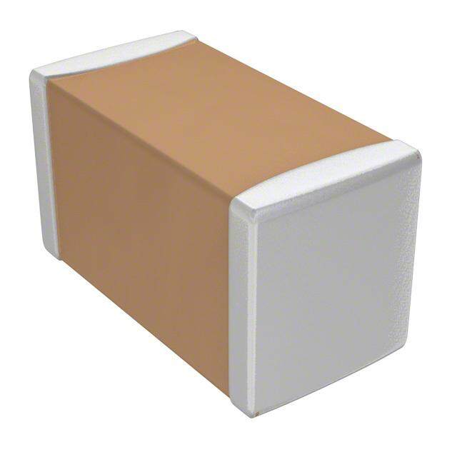
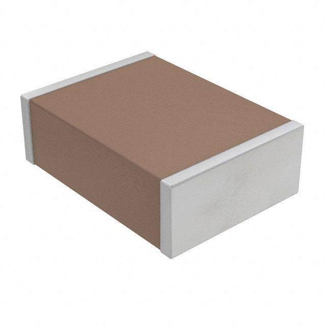
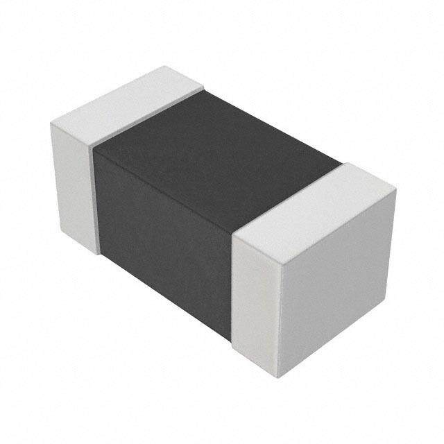
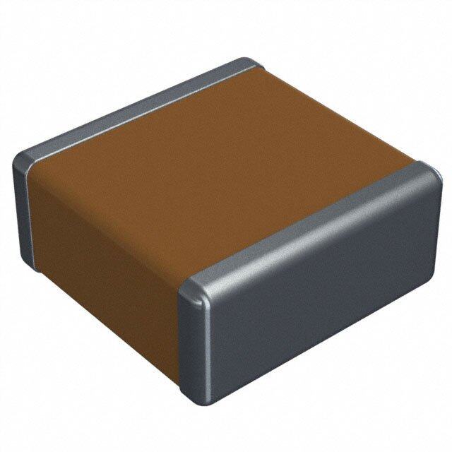
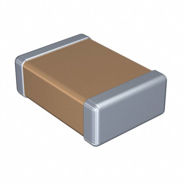
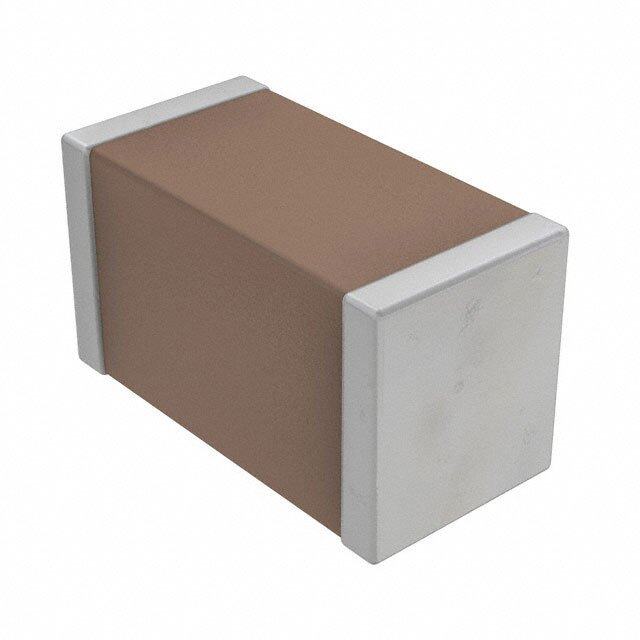
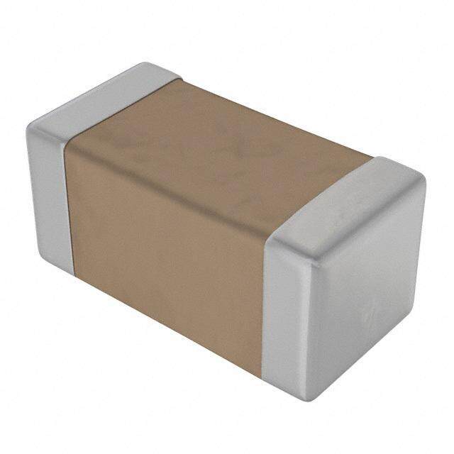
| 产品图片 |
|
| rohs | 符合RoHS无铅 / 符合限制有害物质指令(RoHS)规范要求 |
| 产品系列 | MLCC,多层陶瓷电容器MLCC - SMD/SMT,Murata Electronics GRM32DF51H106ZA01LGRM |
| 数据手册 | |
| 产品型号 | GRM32DF51H106ZA01L |
| 产品 | General Type MLCCs |
| 产品培训模块 | http://www.digikey.cn/PTM/IndividualPTM.page?site=cn&lang=zhs&ptm=5164 |
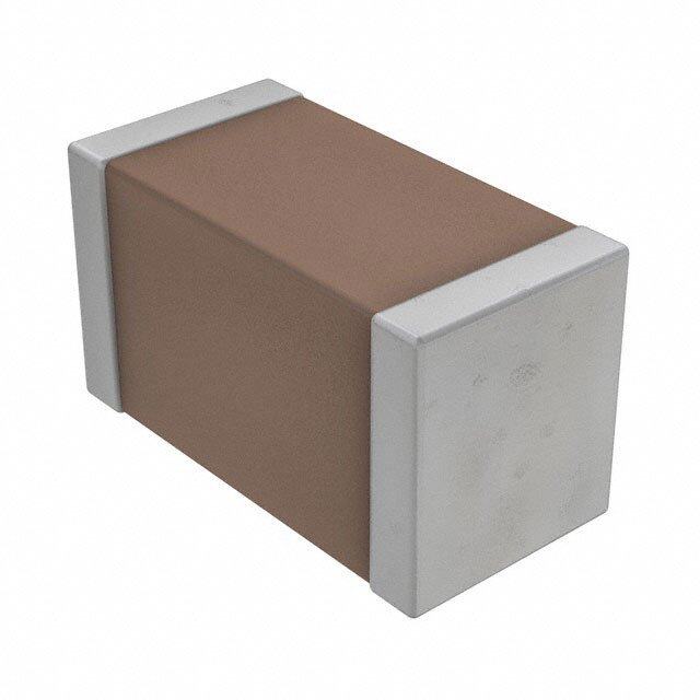
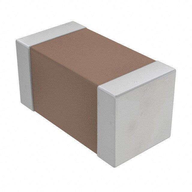
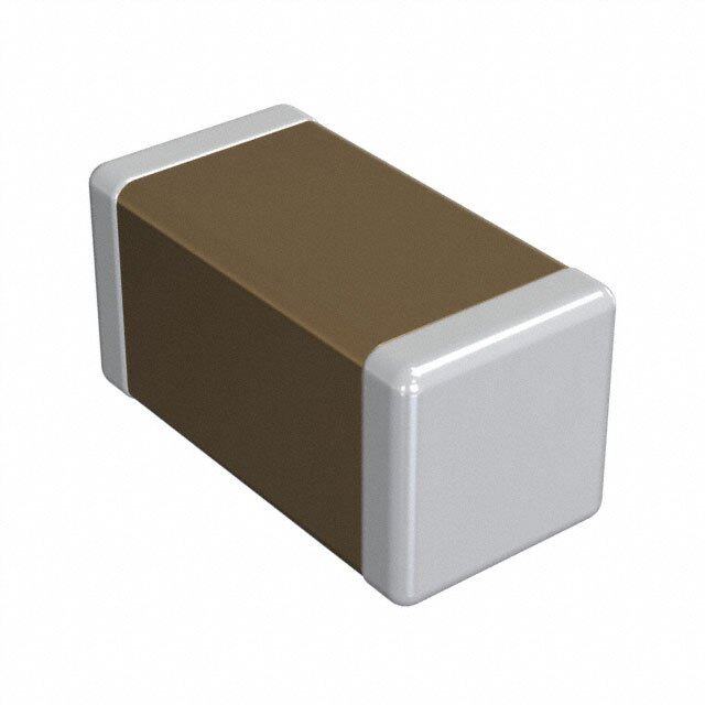
| 产品目录绘图 |
|
| 产品目录页面 | |
| 产品种类 | 多层陶瓷电容器MLCC - SMD/SMT |
| 其它名称 | 490-1891-1 |
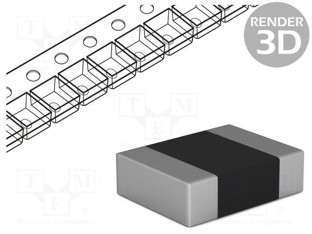
| 包装 | 剪切带 (CT) |
| 厚度(最大值) | 0.087"(2.20mm) |
| 商标 | Murata Electronics |
| 外壳代码-in | 1210 |
| 外壳代码-mm | 3225 |
| 外壳宽度 | 2.5 mm |
| 外壳长度 | 3.2 mm |
| 外壳高度 | 2 mm |
| 大小/尺寸 | 0.126" 长 x 0.098" 宽(3.20mm x 2.50mm) |
| 安装类型 | 表面贴装,MLCC |
| 容差 | - 20 %, + 80 % |
| 封装 | Reel |
| 封装/外壳 | 1210(3225 公制) |
| 封装/箱体 | 1210 (3225 metric) |
| 工作温度 | -30°C ~ 85°C |
| 工作温度范围 | - 30 C to + 85 C |
| 工厂包装数量 | 1000 |
| 应用 | 通用 |
| 引线形式 | - |
| 引线间距 | - |
| 标准包装 | 1 |
| 温度系数 | Y5V(F) |
| 温度系数/代码 | Y5V |
| 特性 | - |
| 特色产品 | http://www.digikey.com/cn/zh/ph/Murata/GA3.html |
| 电压-额定 | 50V |
| 电压额定值 | 50 V |
| 电容 | 10 uF |
| 端接类型 | SMD/SMT |
| 等级 | - |
| 类型 | General Purpose MLCC |
| 系列 | GRM |
| 高度-安装(最大值) | - |


PDF Datasheet 数据手册内容提取
CHIP MONOLITHIC CERAMIC CAPACITOR FOR GENERAL GRM32DF51H106ZA01_ (1210, Y5V, 10uF, 50Vdc) _: packaging code Reference Sheet 1.Scope This product specification is applied to Chip Monolithic Ceramic Capacitor used for General Electronic equipment. 2.MURATA Part NO. System (Ex.) GRM 32 D F5 1H 106 Z A01 L (1)L/W (2)T (3)Temperature (4)DC Rated (5)Nominal (6)Capacitance (7)Murata’s (8)Packaging Dimensions Dimensions Characteristics Voltage Capacitance Tolerance Control Code C o d e 3. Type & Dimensions L W T e g e (Unit:mm) (1)-1 L (1)-2 W (2) T e g 3.2±0.3 2.5±0.2 2.0±0.2 0.3 min. 1.0 min. 4.Rated value (3) Temperature Characteristics Specifications and Test (4) (6) (Public STD Code):Y5V(EIA) (5) Nominal Methods DC Rated Capacitance Temp. coeff Temp. Range Capacitance (Operationg Voltage Tolerance or Cap. Change (Ref.Temp.) Temp. Range) -30 to 85 °C -82 to 22 % 50 Vdc 10 uF +80/-20 % -30 to 85 °C (25 °C) 5.Package mark (8) Packaging Packaging Unit f180mm Reel L 1000 pcs./Reel EMBOSSED W8P4 f330mm Reel K 4000 pcs./Reel EMBOSSED W8P4 Product specifications in this catalog are as of Jan.27,2013,and are subject to change or obsolescence without notice. Please consult the approval sheet before ordering. Please read rating and !Cautions first. GRM32DF51H106ZA01-01 1
■SPECIFICATIONS AND TEST METHODS Specification No Item Temperature High Dielectric Test Method Compensating Type Constant Type 1 Operating △C,1X:-55℃ to 125℃ B1,B3,F1:-25℃ to 85℃ Standard Temperature:20℃ Temperature Range 0C:-55℃ to 150℃ R1,R7,C7:-55℃ to 125℃ (R6,R7,R9,C7,C8,F5,L8:25℃) Other :-25℃ to 85℃ R6:-55℃ to 85℃ R9,L8:-55℃ to 150℃ C8:-55℃ to 105℃ F5:-30℃ to 85℃ 2 Rated Voltage See the previous pages. The rated voltage is defined as the maximum voltage which may be applied continuously to the capacitor. When AC voltage is superimposed on DC voltage, VP-P or VO-P, whichever is larger, should be maintained within the rated voltage range. 3 Appearance No defects or abnormalities. Visual inspection. 4 Dimension Within the specified dimensions. Using calipers. (GRM02 size is based on Microscope) 5 Dielectric Strength No defects or abnormalities. No failure should be observed when 300% of the rated voltage (temperature compensating type) or 250% of the rated voltage (high dielectric constant type) is applied between the terminations for 1 to 5 seconds, provided the charge/discharge current is less than 50mA. 6 Insulation C≦0.047μF:More than 10000MΩ The insulation resistance should be measured with a DC voltage Resistance C>0.047μF:More than 500Ω·F not exceeding the rated voltage at 20℃/25℃ and 75%RH max. C:Nominal Capacitance and within 2 minutes of charging, provided the charge/discharge current is less than 50mA. 7 Capacitance(cid:10)(cid:10)(cid:10)(cid:10)(cid:10) Within the specified tolerance. The capacitance/D.F. should be measured at 20℃/25℃ at the frequency and voltage shown in the table. 8 Q/Dissipation 30pF and over:Q≧1000 [B1,B3,R1,R6,R7,C7,C8,L8] Factor (D.F.) 30pF and below:Q≧400+20CW.V.:100V :0.025max.(C<0.068mF) (1)Temperature Compensating Type :0.05max.(C≧0.068mF) C:Nominal Capacitance(pF) W.V.:50V/25V :0.025max. Capacitance Frequency Voltage W.V.:16V/10V :0.035max. C≦1000pF 1±0.1MHz 0.5 to 5Vrms W.V.:6.3V/4V :0.05max.(C<3.3mF) C>1000pF 1±0.1kHz 1±0.2Vrms :0.1max.(C≧3.3mF) [R9] (2)High Dielectric Constant Type W.V.:50V: 0.05max. [F1,F5] Capacitance Frequency Voltage W.V.:25Vmin C≦10μF 1±0.1kHz 1±0.2Vrms :0.05max. (C<0.1mF) C>10μF 120±24Hz 0.5±0.1Vrms :0.09max.(C≧0.1mF) W.V.:16V/10V:0.125max. W.V.:6.3V:0.15max. 9 Capacitance No bias Within the specified B1,B3 : Within ±10% The capacitance change should be measured after 5min. at each Temperature tolerance.(Table A) (-25°C to +85°C) specified temp.stage. Characteristics R1,R7 : Within ±15% (1)Temperature Compensating Type (-55°C to +125°C) The temperature coefficient is determind using the capacitance R6 : Within ±15% measured in step 3 as a reference. (-55°C to +85°C) When cycling the temperature sequentially from step 1 through R9 : Within ±15% 5 (ΔC:+20℃ to +125℃:other temp.coeffs.:+20℃ to +85℃) the (-55°C to +150°C) capacitance should be within the specified tolerance for the C7 : Within ±22% temperature coefficient and capacitance change as Table A-1. (-55°C to +125°C) The capacitance drift is caluculated by dividing the differences C8 : Within ±22% between the maximum and minimum measured values in the (-55°C to +105°C) step 1 ,3 and 5 by the cap.value in step 3. F1 : Within +30/-80% Step Temperature(C) (-25°C to +85°C) F5 :Within +22/-82% 1 20±2 (-30°C to +85°C) 2 -55±3(for C)/-25±3(for other TC) L8 : Within ±15% 3 20±2 (-55°C to +125°C) 125±3(for 2C/3C/4C) : Within +15/-40% 4 150±3(for 0C) 85±3(for other TC) (+125°C to +150°C) 50% of B1: Within +10/-30% 5 20±2 the rated R1: Within +15/-40% voltage F1: Within +30/-95% 2) High Dielectric Constant Type The ranges of capacitance change compared with the 20℃ value over the temperature ranges shown in the table should be CapacitanceWithin±0.2% or±0.05pF within the specified ranges.* Drift (Whichever is larger.) In case of applying voltage, the capacitance change should be *Not apply to 1X/25V measured after 1 more min. with applying voltage in equilibration of each temp. stage. Applying Step Temperature(℃) voltage 1 20±2/25±2 *Initial measurement for high -55±3(for R1,R7,R6,R9,C7,C8,L8)/ dielectric constant type 2 -25±3(for B1,B3,F1)/ Perform a heat treatment at 150 -30±3(for F5) No bias +0/-10℃ for one hour and then 3 20±2/25±2 set for 24±2 hours at room 4 125±3(for R1,R7,C7)/150±3(for R9,L8) 105±3(for C8)/85±3(for B1,B3,R6,F1,F5) temperature. 5 20±2 Perform the initial measure-ment. 6 -55±3(for R1)/-25±3(for B1,F1) 50% of the 7 20±2 rated voltage 8 125±3(for R1)/85±3(for B1,F1) JEMCGS-0001S 2
■SPECIFICATIONS AND TEST METHODS Specification No Item Temperature High Dielectric Test Method Compensating Type Constant Type 10 Adhesive Strength No removal of the terminations or other defect should occur. Solder the capacitor on the test jig (glass epoxy board)shown in of Termination Fig.3 using an eutectic solder. Then apply 10N* force in parallel with the test jig for 10±1seconds. The soldering should be done either with an iron or using the reflow method and should be conducted with care so that the soldering is uniform and free of defects such as heat shock. *1N(GRM02),2N(GRM03),5N(GRM15,GRM18) 11 Vibration (cid:10) Appearance No defects or abnormalities. Solder the capacitor on the test jig (glass epoxy board) in the same Resistance manner and under the same conditions as (10). Capacitance Within the specified tolerance. The capacitor should be subjected to a simple harmonic motion having a total amplitude of 1.5mm, the frequency being varied Q/D.F. 30pF and over:Q≧1000 [B1,B3,R1,R6,R7,C7,C8,L8] uniformly between the approximate limits of 10 and 55Hz. The 30pF and beloow:Q≧400+20C W.V.:100V :0.025max.(C<0.068mF) frequency range, from 10 to 55Hz and return to 10Hz, should be :0.05max.(C≧0.068mF) traversed in approximately 1 minute. This motion should be C:Nominal Capacitance(pF) W.V.:50V/25V :0.025max. applied for a period of 2 hours in each 3 mutually perpendicular W.V.:16V/10V :0.035max. directions(total of 6 hours). W.V.:6.3V/4V :0.05max. (C<3.3mF) :0.1max.(C≧3.3mF) [R9] W.V.:50V: 0.05max. [F1,F5] W.V.:25Vmin :0.05max. (C<0.1mF) :0.09max. (C≧0.1mF) W.V.:16V/10V:0.125max. W.V.:6.3V:0.15max. 12 Deflection Appearance No defects or abnormalities. Solder the capacitor on the test jig (glass epoxy board) shown in Fig.1 using an eutectic solder. Then apply a force in the direction Capacitance Within ±5% or± 0.5pF Within ±10% shown in Fig 2 for 5±1 seconds. The soldering should be done Change (Whichever is larger) by the reflow method and should be conducted with care so that the soldering is uniform and free of defects such as heat shock. 13 Solderability 75% of the terminations is to be soldered evenly and continuously. Immerse the capacitor in a solution of ethanol (JIS-K-8101) and of Termination rosin (JIS-K-5902) (25% rosin in weight propotion) . Preheat at 80 to 120℃ for 10-to 30 seconds. After preheating, immerse in an eutectic solder solution for 2±0.5 seconds at 230±5℃ or Sn-3.0Ag-0.5Cu solder solution for 2±0.5 seconds at 245±5℃. 14 Resistance to Appearance No defects or abnormalities. Preheat the capacitor at 120 to 150℃ for 1 minute. Soldering Heat Immerse the capacitor in an eutectic solder solution* or Capacitance Within ±2.5% or± 0.25pF B1,B3,R1,R6,R7,R9,C7,C8,L8:Within ±7.5% Sn-3.0Ag-0.5Cu solder solution at 270±5℃ for 10±0.5 seconds. Change (Whichever is larger) F1,F5 :Within ±20% Set at room temperature for 24±2 hours, then measure. Q/D.F. 30pF and over:Q≧1000 [B1,B3,R1,R6,R7,C7,C8,L8] *Not apply to GRM02 30pF and beloow:Q≧400+20C W.V.:100V :0.025max.(C<0.068mF) :0.05max.(C≧0.068mF) · Initial measurement for high dielectric constant type C:Nominal Capacitance(pF) W.V.:50V/25V :0.025max. Perform a heat treatment at 150+0/-10C for one hour and then set W.V.:16V/10V :0.035max. at room temperature for 24±2 hours. W.V.:6.3V/4V :0.05max. (C<3.3mF) Perform the initial measurement. :0.1max.(C≧3.3mF) [R9] *Preheating for GRM32/43/55 W.V.:50V: 0.05max. Table1 [F1,F5] Step Temperature Time W.V.:25Vmin 1 100C to 120C 1 min. :0.05max. (C<0.1mF) :0.09max. (C≧0.1mF) 2 170C to 200C 1 min. W.V.:16V/10V:0.125max. W.V.:6.3V:0.15max. I.R. More than 10,000MW or 500W·F(Whichever is smaller) Dielectric No defects. Strength 15 Temperature Appearance No defects or abnormalities. Fix the capacitor to the supporting jig in the same Cycle manner and under the same conditions as (10). Capacitance Within ±2.5% or± 0.25pF B1,B3,R1,R6,R7,R9,C7,C8,L8:Within ±7.5% Perform the five cycles according to the four heat Change (Whichever is larger) F1,F5 :Within ±20% treatments shown in the following table. Q/D.F. 30pF and over:Q≧1000 [B1,B3,R1,R6,R7,C7,C8,L8] Set for 24±2 hours at room temperature, then measure. 30pF and beloow:Q≧400+20C W.V.:100V :0.025max.(C<0.068mF) :0.05max.(C≧0.068mF) Step Temp.(C) Time (min) C:Nominal Capacitance(pF) W.V.:50V/25V :0.025max. 1 Min. 30±3 W.V.:16V/10V :0.035max. Operating Temp.+0/-3 W.V.:6.3V/4V :0.05max. (C<3.3mF) 2 Room Temp 2 to 3 :0.1max.(C≧3.3mF) 3 Max. 30±3 [R9] Operating Temp.+3/-0 W.V.:50V: 0.05max. 4 Room Temp 2 to 3 [F1,F5] W.V.:25Vmin · Initial measurement for high dielectric constant type :0.05max. (C<0.1mF) Perform a heat treatment at 150+0/-10C for one hour and then set :0.09max. (C≧0.1mF) at room temperature for 24±2 hours. W.V.:16V/10V:0.125max. Perform the initial measurement. W.V.:6.3V:0.15max. I.R. More than 10,000MW or 500W·F(Whichever is smaller) Dielectric No defects. Strength JEMCGS-0001S 3
■SPECIFICATIONS AND TEST METHODS Specification No Item Temperature High Dielectric Test Method Compensating Type Constant Type 16 Humidity Appearance No defects or abnormalities. Set the capacitor at 40±2℃ and in 90 to 95% humiduty (Steady State) for 500±12 hours. Capacitance Within ±5% or± 0.5pF B1,B3,R1,R6,R7,R9,C7,C8,L8:Within ±12.5% Remove and set for 24±2 hours at room temperature, Change (Whichever is larger) F1,F5 :Within ±30% then measure. Q/D.F. 30pF and over:Q≧350 [B1,B3,R1,R6,R7,C7,C8,L8] 10pF and over W.V.:100V :0.05max.( C<0.068mF) 30pF and below:Q≧275+5C/2 :0.075max.(C≧0.068mF) 10pF and below:Q≧200+10C W.V.:50V/25V :0.05max. W.V.:16V/10V :0.05max. C:Nominal Capacitance(pF) W.V.:6.3V/4V :0.075max.(C<3.3mF) :0.125max.(C≧3.3mF) [R9] W.V.:50V: 0.075max. [F1,F5] W.V.:25Vmin :0.075max. (C<0.1mF) :0.125max. (C≧0.1mF) W.V.:16V/10V:0.15max. W.V.:6.3V:0.2max. I.R. More than 1,000MW or 50W·F(Whichever is smaller) 17 Humidity Load Appearance No defects or abnormalities. Apply the rated voltage at 40±2℃ and 90 to 95% humidity for 500±12 hours. Remove and set for 24±2 hours at room Capacitance Within ±7.5% or±0.75pF B1,B3,R1,R6,R7,R9,C7,C8,L8:Within ±12.5% temprature, then muasure. The charge/discharge current Change (Whichever is larger) F1,F5 :Within ±30% is less than 50mA. [W.V.:10Vmax.] F1 :Within+30/-40% Q/D.F. 30pF and over:Q≧200 [B1,B3,R1,R6,R7,C7,C8,L8] • Initial measurement for F1/10Vmax. 30pF and below:Q≧100+10C/3W.V.:100V :0.05max.( C<0.068mF) Apply the rated DC voltage for 1 hour at 40±2℃. :0.075max.(C≧0.068mF) Remove and set for 24±2 hours at room temperature. C:Nominal Capacitance(pF) W.V.:50V/25V :0.05max. Perform initial measurement. W.V.:16V/10V :0.05max. W.V.:6.3V/4V :0.075max.(C<3.3mF) :0.125max.(C≧3.3mF) [R9] W.V.:50V: 0.075max. [F1,F5] W.V.:25Vmin :0.075max. (C<0.1mF) :0.125max. (C≧0.1mF) W.V.:16V/10V:0.15max. W.V.:6.3V:0.2max. I.R. More than 500MΩ or 25Ω·F(Whichever is smaller) 18 High TemperatureAppearance No defects or abnormalities. Apply 200% of the rated voltage at the maximum Load operating temperature±3℃ for 1000±12 hours. Capacitance Within ±3% or ±0.3pF B1,B3,R1,R6,R7,R9,C7,C8,L8:Within ±12.5% Set for 24±2 hours at room temperature, then measure. Change (Whichever is larger) F1,F5 :Within ±30% The charge/discharge current is less than 50mA. [Except 35V,10Vmax and C≧1.0. mF] F1 :Within+30/-40% [35V, 10Vmax and C≧1.0. mF] Q/D.F. 30pF and over:Q≧350 [B1,B3,R1,R6,R7,C7,C8,L8] ・Initial measurement for high dielectric constant type. 10pF and over W.V.:100V :0.05max.( C<0.068mF) Apply 200% of the rated DC voltage at the maximun operating 30pF and below: Q≧275+5C/2 :0.075max.(C≧0.068mF) temperature ±3°C for one hour. Remove and set for 10pF and below:Q≧200+10C W.V.:50V/25V :0.05max. 24±2 hours at room temperature. W.V.:16V/10V :0.05max. Perform initial measurement. C:Nominal Capacitance (pF) W.V.:6.3V/4V :0.075max.(C<3.3mF) :0.125max.(C≧3.3mF) [R9] W.V.:50V: 0.075max. [F1,F5] W.V.:25Vmin :0.075max. (C<0.1mF) :0.125max. (C≧0.1mF) W.V.:16V/10V:0.15max. W.V.:6.3V:0.2max. I.R. More than 1,000MW or 50W·F(Whichever is smaller) Table A Nominal Capacitance Change from 20C (%) Char. Values -55 -25 -10 (ppm/C) * Max. Min. Max. Min. Max. Min. 2C/0C 0± 60 0.82 -0.45 0.49 -0.27 0.33 -0.18 3C 0±120 1.37 -0.90 0.82 -0.54 0.55 -0.36 4C 0±250 2.56 -1.88 1.54 -1.13 1.02 -0.75 2P -150± 60 - - 1.32 0.41 0.88 0.27 3P -150±120 - - 1.65 0.14 1.10 0.09 4P -150±250 - - 2.36 -0.45 1.57 -0.30 2R -220± 60 - - 1.70 0.72 1.13 0.48 3R -220±120 - - 2.03 0.45 1.35 0.30 4R -220±250 - - 2.74 -0.14 1.83 -0.09 2S -330± 60 - - 2.30 1.22 1.54 0.81 3S -330±120 - - 2.63 0.95 1.76 0.63 4S -330±250 - - 3.35 0.36 2.23 0.24 2T -470± 60 - - 3.07 1.85 2.05 1.23 3T -470±120 - - 3.40 1.58 2.27 1.05 4T -470±250 - - 4.12 0.99 2.74 0.66 3U -750±120 - - 4.94 2.84 3.29 1.89 4U -750+250 - - 5.65 2.25 3.77 1.50 1X +350 to -1000 - - - - - - * Nominal values denote the temperature coefficient within a range of 20C to 125C(for C)/ 150C(for 0C)/85C(for other TC). JEMCGS-0001S 4
■SPECIFICATIONS AND TEST METHODS Adhesive Strength of Termination,Vibration Resistance,Temperature Cycle, Test method : Deflection Humidity ,Humidity Load,High Temperature Load ・Test substrate ・Test substrate Material : Copper-clad laminated sheets for PCBs Material : Copper-clad laminated sheets for PCBs (Glass fabric base, epoxy resin) (Glass fabric base, epoxy resin) Thickness : 1.6mm (GRM02/03/15: t:0.8mm) Thickness : 1.6mm (GRM02/03/15: t:0.8mm) Copper foil thickness : 0.035mm Copper foil thickness : 0.035mm Gray colored part of Fig.1: Solder resist ラ ン ト L ゙ a n d b ( Cbo at with heat rfef s4i4s.t.a55n t resin for soldr) b *1,c2: 2.0±a φ0.10.55+-00.1 *4.10±*0.21 1.75±0.1 *1,2:2.0±φ0.10.55+-00.1 *4.10±*0.21 1.75±0.1 c c a 40 Glass epoxy boAaBrd SBcooaplkdpeeedrr r efeolesilic sttr ode or 3.5±0.05 8.0±0.3 AB 3.5±0.05 8.0±0.3 c 100 0.05以下 0.05以下 t t Fig.1 (in:mm) Fig.3 (in:mm) Dimension (mm) Dimension (mm) Type Type a b c a b c GRM02 0.2 0.56 0.23 GRM02 0.2 0.56 0.23 GRM03 0.3 0.9 0.3 GRM03 0.3 0.9 0.3 GRM15 0.4 1.5 0.5 GRM15 0.4 1.5 0.5 GRM18 1.0 3.0 1.2 GRM18 1.0 3.0 1.2 GRM21 1.2 4.0 1.65 GRM21 1.2 4.0 1.65 GRM31 2.2 5.0 2.0 GRM31 2.2 5.0 2.0 GRM32 2.2 5.0 2.9 GRM32 2.2 5.0 2.9 GRM43 3.5 7.0 3.7 GRM43 3.5 7.0 3.7 GRM55 4.5 8.0 5.6 GRM55 4.5 8.0 5.6 Pressurization 20 50 speed 1.0mm/s Pressurize Capacitor R230 45 45 Support Flexure:≦1 Capacitance meter 45 45 Fig.2 (in:mm) JEMCGS-0001S 5
Package GRM/F Type 1.Tape Carrier Packaging(Packaging Code:D/E/W/F/L/J/K) 1.1 Minimum Quantity(pcs./reel) φ180mm reel φ330mm reel Type Paper Tape Plastic Tape Paper Tape Plastic Tape Code:D/E Code:W Code:L Code:J/ F Code:K GR□02 40000 (W4P1) GR□03 15000(W8P2) 30000(W8P1) 50000(W8P2) 2 20000 50000 3/X 10000 50000 GR□15 5 (Dimensions Tolerance:±0.05) 10000(W8P2) 20000(W8P1) 50000(W8P2) 5 (Dimensions Tolerance:±0.1min.) 10000 40000 GR□18 4000 10000 5/6/9 4000 3000 10000 GR□21 A/B 3000 10000 6/9 4000 10000 GR□31 M/X 3000 10000 C 2000 6000 5/6/9 4000 10000 A/M 3000 10000 GR□32 N 2000 8000 C 2000 6000 R/D/E 1000 4000 M 1000 5000 N/C/R/D 1000 4000 GR□43 E 500 2000 S 500 1500 M 1000 5000 N/C/R/D 1000 4000 GR□55 E 500 F/X 300 1500 1.2 Dimensions of Tape (1)GR□02 (W4P1 CODE:L) (in:mm) *1,2:1.0±0.0φ2 0.8±0.04 2*.10 ±0.0*42 0.9±0.05 0.15~0.4 *1,2:1.0±0.0φ20.8±0.04 *2.10±0*.024 0.9±0.05 0.15~0.4 A B 1.8±0.02 4.0±0.05 AB 1.8±0.02 4.0±0.05 0.05 max. 0.05以下 t t Code GR□02 A *3 0.23 B *3 0.43 *3 Nominal value t 0.5 max. JEMCGP-01796 6
Package GRM/F Type (in:mm) (2)GR□03/15(W8P2 CODE:D/E/J/F) *1,2:2.0±0.05 4.0±0.1 1 *1,2:2.0±0.05 4.0±0.1 .1 . 0 0 ± ± φ1.5 +- 00. 1 *1 *2 1.75 φ1.5+-00.1 *1 *2 1.75 A B 3.5±0.05 8.0±0.3 AB 3.5±0.05 8.0±0.3 0.05 max. 0.05以下 t t GR□03 GR□03 GR□15 GR□15 GR□15 GR□15 (Dimensions (Dimensions (Dimensions (Dimensions (Dimensions (Dimensions Code Tolerance Tolerance Tolerance Tolerance Tolerance Tolerance ±0.03) ±0.05) ±0.05) ±0.1) ±0.15) ±0.2) A*3 0.37 0.39 0.65 0.70 0.72 0.75 B*3 0.67 0.69 1.15 1.20 1.25 1.35 t 0.5max. 0.5 max. 0.8 max. 0.8 max. 0.8 max. 0.8 max. *3 Nominal value (3)GRM03/15(W8P1 CODE:W) (in:mm) 4.0±0.1 1 . 0 1.0±0.05 ± φ1.5 +- 00. 1 .75 1 5 .0 A ±0 .3 0 5 ± . B 3 .0 8 1.0±0.05 t Code GRM03 GRM15 A* 0.37 0.65 B* 0.67 1.15 t 0.5max. 0.8max. *Nominal value JEMCGP-01796 7
Package GRM/F Type (4)GR□18/21/31/32 T:0.85 rank max. (in:mm) 4.0±0.1 4.0±0.1 1 . 0 2.0±0.1 ± φ1.5 + 0.1 5 -0 7 . 1 5 A ±0.0 0.3 5 ± B 3. .0 8 0.8 max.(T=0.5mm) 1.15 max.(T≦0.85mm) GR□18 GR□18 GR□18 Code (Dimensions Tolerance (Dimensions Tolerance (Dimensions Tolerance GR□21 GR□31 GR□32 ±0.15within) ±0.2) L:±0.2/ W,T:±0.1) A 1.05±0.1 1.10±0.1 1.05±0.1 1.55±0.15 2.0±0.2 2.8±0.2 B 1.85±0.1 2.00±0.1 2.00±0.1 2.3±0.15 3.6±0.2 3.6±0.2 (5)GR□21/31/32 T:1.0 rank min. (in:mm) 4.0±0.1 4.0±0.1 1 . 0 0.25±0.1(T≦2.0mm) 2.0±0.1 ± φ1.5 + 0.1 75 0.3±0.1(T:2.5mm) -0 . 1 5 A ±0.0 0.3 ± 5 B 3. .0 8 * 1.7 max.(T≦1.25mm) 2.5 max. (T:1.35/1.6mm) 3.0 max. (T:1.8/2.0mm) 3.7 max. (T≧2.5mm) * GR□21 GR□21 GR□31 GR□31 Code (Dimensions Tolerance: (Dimensions Tolerance : (Dimensions Tolerance: (Dimensions Tolerance: GR□32 ±0.1) ±0.15 /±0.2) ±0.2 within) ±0.3) A 1.45±0.2 1.5±0.2 1.9±0.2 2.1±0.2 2.8±0.2 B 2.25±0.2 2.3±0.2 3.5±0.2 3.6±0.2 3.5±0.2 JEMCGP-01796 8
Package GRM/F Type (6)GR□43/55 (in:mm) 1 . 0 ± 8.0±0.1 * 4.0±0.1 φ1.5 +- 00. 1 1.75 0.3±0.1 *:2.0±0.1 1 A ±0. 3 . 5 0 . ± 5 0 B . 2 1 *1 4.0±0.1 +0.2 φ1.5 - 0 2.5 max.(T≦1.8mm) 2.0±0.1 3.7 max.(T=2.0/2.5mm) 4.7 max.(T≧2.8mm) *1 Code GR□43 GR□55 A *2 3.6 5.2 B *2 4.9 6.1 *2 Nominal value JEMCGP-01796 9
図1 チ ップ詰め状態 (単 位:m m) Package GRM/F Type Fig .1 Package Chips (in:mm) Chip Fig.2 Dimensions of Reel 2.0±0.5 φ21±0.8 0/-3.0 ±2.0 min. 0.5 180+ φ330 φ50 φ13± φ w1 W W w 1 Fig.3 Taping Diagram GR□02 8.0 max. 5±1.5 GR□32 max. 16.5 max. 10±1.5 GR□43/55 20.5 max. 14±1.5 Top Tape : Thickness 0.06 Feeding Hole :As specified in 1.2. Hole for Chip : As specified in 1.2. Bottom Tape :Thickness 0.05 (Only a bottom tape existence ) Base Tape : As specified in 1.2. JEMCGP-01796 10
Package 図1 チ ップ詰め状態 (単 位:m m) GRM/F Type 1.3 Tapes for capacitors are wound clockwise shown in Fig.3. (The sprocket holes are to the right as the tape is pulled toward the user.) 1.4 Part of the leader and part of the vacant section are attached as follows. Tail vacant Section Chip-mounting Unit Leader vacant Section (in:mm) Leader Unit (Top Tape only) Direction of Feed 160 min. 190 min. 210 min. 1.5 Accumulate pitch : 10 of sprocket holes pitch = 40±0.3mm 1.6 Chip in the tape is enclosed by top tape and bottom tape as shown in Fig.1. 1.7 The top tape and base tape are not attached at the end of the tape for a minimum of 5 pitches. 1.8 There are no jointing for top tape and bottom tape. 1.9 There are no fuzz in the cavity. 1.10 Break down force of top tape : 5N min. Break down force of bottom tape : 5N min. (Only a bottom tape existence ) 図1 チ ッフ 1゚詰.1め1 状Re態e l is made by resin and appeaser and dime(n単 si位on: m ism )s h own in Fig 2. There are possibly to change the material and d imension due to some impairment. 1.12 Peeling off force : 0.1N to 0.6N* in the direction as shown below. * GR□02/03:0.05N~0.5N 165~180° Top tape 1.13 Label that show the customer parts number, our parts number, our company name, inspection number and quantity, will be put in outside of reel. JEMCGP-01796 11
! Caution ■ Limitation of use Please contact our sales representatives or product engineers before using our products for the applications listed below which require of our products for other applications than specified in this product. ①Aircraft equipment ②Aerospace equipment ③Undersea equipment ④Power plant control equipment ⑤Medical equipment ⑥Transportation equipment(vehicles,trains,ships,etc.) ⑦Traffic signal equipment ⑧Disaster prevention / crime prevention equipment ⑨Data-processing equipment ⑩Application of similar complexity and/or requirements to the applications listed in the above ■ Storage and Operation condition 1. The performance of chip monolithic ceramic capacitors may be affected by the storage conditions. 1-1. Store capacitors in the following conditions: Temperature of +5℃ to +40℃ and a Relative Humidity of 20% to 70%. (1) Sunlight, dust, rapid temperature changes, corrosive gas atmosphere or high temperature and humidity conditions during storage may affect the solderability and the packaging performance Please use product within six months of receipt. (2) Please confirm solderability before using after six months. Store the capacitors without opening the original bag. Even if the storage period is short, do not exceed the specified atmospheric conditions. 1-2. Corrosive gas can react with the termination (external) electrodes or lead wires of capacitors, and result in poor solderability. Do not store the capacitors in an atmosphere consisting of corrosive gas (e.g., hydrogen sulfide, sulfur dioxide, chlorine, ammonia gas etc.). 1-3. Due to moisture condensation caused by rapid humidity changes, or the photochemical change caused by direct sunlight on the terminal electrodes and/or the resin/epoxy coatings, the solderability and electrical performance may deteriorate. Do not store capacitors under direct sunlight or in high huimidity conditions JEMCGC-2701V 12
! Caution ■Rating 1.Temperature Dependent Characteristics 1. The electrical characteristics of the capacitor can change with temperature. 1-1. For capacitors having larger temperature dependency, the capacitance may change with temperature changes. The following actions are recommended in order to insure suitable capacitance values. (1) Select a suitable capacitance for the operating temperature range. (2) The capacitance may change within the rated temperature. When you use a high dielectric constant type capacitors in a circuit that needs a tight (narrow) capacitance tolerance. Example: a time constant circuit., please carefully consider the characteristics of these capacitors, such as their aging, voltage, and temperature characteristics. And check capacitors using your actual appliances at the intended environment and operating conditions. □ Typical temperature characteristics Char.R6 (X5R) □ Typical temperature characteristics Char.R7 (X7R) 20 20 hange (%) 11055 nge (%) 11550 e C 0 Cha 0 pacitanc --11-505 acitance -1-50 a p -15 C -20 Ca -20 -75 -50 -25 0 25 50 75 100 -75 -50 -25 0 25 50 75 100 125 150 Temperature (℃) Temperature (℃) □ Typical temperature characteristics Char.F5 (Y5V) 40 %) 20 e ( 0 g n a -20 h C e -40 c an -60 cit a -80 p a C-100 -50 -25 0 25 50 75 100 Temperature (℃) 2.Measurement of Capacitance 1. Measure capacitance with the voltage and the frequency specified in the product specifications. 1-1. The output voltage of the measuring equipment may decrease when capacitance is high occasionally. Please confirm whether a prescribed measured voltage is impressed to the capacitor. 1-2. The capacitance values of high dielectric constant type capacitors change depending on the AC voltage applied. Please consider the AC voltage characteristics when selecting a capacitor to be used in a AC circuit. JEMCGC-2701V 13
! Caution 3.Applied Voltage 1. Do not apply a voltage to the capacitor that exceeds the rated voltage as called-out in the specifications. 1-1. Applied voltage between the terminals of a capacitor shall be less than or equal to the rated voltage. (1) When AC voltage is superimposed on DC voltage, the zero-to-peak voltage shall not exceed the rated DC voltage. When AC voltage or pulse voltage is applied, the peak-to-peak voltage shall not exceed the rated DC voltage. (2) Abnormal voltages (surge voltage, static electricity, pulse voltage, etc.) shall not exceed the rated DC voltage. Typical voltage applied to the DC capacitor DC voltage DC voltage+AC AC voltage Pulse voltage E E E 0 E 0 0 0 (E:Maximum possible applied voltage.) 1-2. Influence of overvoltage Overvoltage that is applied to the capacitor may result in an electrical short circuit caused by the breakdown of the internal dielectric layers . The time duration until breakdown depends on the applied voltage and the ambient temperature. 4. Applied Voltage and Self-heating Temperature 1. When the capacitor is used in a high-frequency voltage, pulse voltage, application, be sure to take into account self-heating may be caused by resistant factors of the capacitor. 1-1. The load should be contained to the level such that when measuring at atomospheric temperature of 25℃,the product's self-heating remains below 20℃ and surface temperature of the capacitor in the actual circuit remains wiyhin the maximum operating temperature. JEMCGC-2701V 14
Caution ! 5. DC Voltage and AC Voltage Characteristic 1. The capacitance value of a high dielectric constant type capacitor changes depending on the DC voltage applied. Please consider the DC voltage characteristics when a capacitor is selected for use in a DC circuit. 1-1. The capacitance of ceramic capacitors may change sharply depending on the applied voltage. (See figure) Please confirm the following in order to secure the capacitance. (1) Whether the capacitance change caused by the applied voltage is within the range allowed or not. □ DC voltage characteristics 20 (2) In the DC voltage characteristics, the rate of capacitance %) 0 change becomes larger as voltage increases. e( Even if the applied voltage is below the rated voltage. ng -20 a h When a high dielectric constant type capacitor is in a C -40 e circuit that needs a tight (narrow) capacitance tolerance. anc -60 Example: a time constant circuit., please carefully cit pa -80 consider the characteristics of these capacitors, such as Ca -100 their aging, voltage, and temperature characteristics. 0 1 2 3 4 5 6 7 And check capacitors using your actual appliances at the intended environment and operating conditions. DC Voltage (VDC) 2. The capacitance values of high dielectric constant type capacitors change depending on the AC voltage applied. Please consider the AC voltage characteristics when selecting a capacitor to be used in a AC circuit. □ AC voltage characteristics 30 %) 20 e ( 10 g n 0 a Ch -10 e -20 c n a -30 acit -40 p Ca -50 -60 0.0 0.5 1.0 1.5 2.0 2.5 6. Capacitance Aging AC Voltage (Vr.m.s.) 1. The high dielectric constant type capacitors have the characteristic in which the capacitance value decreases with passage of time. When you use a high dielectric constant type capacitors in a circuit that needs a tight (narrow) capacitance tolerance. Example: a time constant circuit., please carefully consider the characteristics of these capacitors, such as their aging, voltage, and temperature characteristics. And check capacitors using your actual appliances at the intended environment and operating conditions. 20 %) 10 e ( ng 0 a h C e -10 nc acita -20 5C ap RΔ C -30 -40 10.0 100.0 1000.0 10000.0 Time(Hr) JEMCGC-2701V 15
! Caution 7.Vibration and Shock 1. Please confirm the kind of vibration and/or shock, its condition, and any generation of resonance. Please mount the capacitor so as not to generate resonance, and do not allow any impact on the terminals. 2. Mechanical shock due to falling may cause damage or a crack in the dielectric material of the capacitor. Do not use a fallen capacitor because the quality and reliability may be deteriorated. Crack Floor 3. When printed circuit boards are piled up or handled, the corners of another printed circuit board should not be allowed to hit the capacitor in order to avoid a crack or other damage to the capacitor. Mounting printed circuit board Crack ■ Soldering and Mounting 1.Mounting Position 1. Confirm the best mounting position and direction that minimizes the stress imposed on the capacitor during flexing or bending the printed circuit board. 1-1.Choose a mounting position that minimizes the stress imposed on the chip during flexing or bending of the board. [Component Direction] ① Locate chip horizontal to the direction in which stress acts 1A [Chip Mounting Close to Board Separation Point] ① C Perforation B Chip arrangement D Worst A-C-(B~D) Best 1A A Slit 1B ③ ② 1C JEMCGC-2701V 16
! Caution 2.Information before mounting 1. Do Not re-use capacitors that were removed from the equipment. 2. Confirm capacitance characteristics under actual applied voltage. 3. Confirm the mechanical stress under actual process and equipment use. 4. Confirm the rated capacitance, rated voltage and other electrical characteristics before assembly. 5. Prior to use, confirm the Solderability for the capacitors that were in long-term storage. 6. Prior to measuring capacitance, carry out a heat treatment for capacitors that were in long-term storage. 7.The use of Sn-Zn based solder will deteriorate the reliability of the MLCC. Please contact our sales representative or product engineers on the use of Sn-Zn based solder in advance. 3.Maintenance of the Mounting (pick and place) Machine 1. Make sure that the following excessive forces are not applied to the capacitors. 1-1. In mounting the capacitors on the printed circuit board, any bending force against them shall be kept to a minimum to prevent them from any bending damage or cracking. Please take into account the following precautions and recommendations for use in your process. (1) Adjust the lowest position of the pickup nozzle so as not to bend the printed circuit board. (2) Adjust the nozzle pressure within a static load of 1N to 3N during mounting. Suction Nozzle [Incorrect] Deflection Board Board Guide [Correct] Support Pin 2.Dirt particles and dust accumulated between the suction nozzle and the cylinder inner wall prevent the nozzle from moving smoothly. This imposes greater force upon the chip during mounting, causing cracked chips. Also the locating claw, when worn out, imposes uneven forces on the chip when positioning, causing cracked chips. The suction nozzle and the locating claw must be maintained, checked and replaced periodically. JEMCGC-2701V 17
! Caution 4-1.Reflow Soldering 1. When sudden heat is applied to the components, the [Standard Conditions for Reflow Soldering] mechanical strength of the components will decrease because a sudden temperature change causes Infrared Reflow deformation inside the components. In order to prevent mechanical damage to the components, preheating is Temperature(℃) Soldering Peak Temperature required for both the components and the PCB board. 200℃ GCoraodliunagl Preheating conditions are shown in table 1. It is required to ΔT keep the temperature differential between the solder and 170℃ 150℃ the components surface (ΔT) as small as possible. 130℃ Preheating 2. Solderability of Tin plating termination chips might be deteriorated when a low temperature soldering profile where Time 60-120 seconds 30-60 seconds the peak solder temperature is below the melting point of Tin is used. Please confirm the Solderability of Tin plated termination chips before use. Vapor Reflow Temperature(℃) 3. When components are immersed in solvent after mounting, Peak Temperature Soldering be sure to maintain the temperature difference (ΔT) Gradual between the component and the solvent within the range ΔT Cooling shown in the table 1. 170℃ 150℃ 130℃ Table 1 Preheating Part Number Temperature Differential Time 60-120 seconds 20 seconds max. GR□02/03/15/18/21/31 ΔT≦190℃ [Allowable Soldering Temperature and Time] 280 GR□32/43/55 ΔT≦130℃ ℃) erature( 227600 p Tem 250 ng 240 eri Recommended Conditions old 230 Pb-Sn Solder S 220 0 30 60 90 120 Lead Free Solder Soldering Time(sec.) Infrared Reflow Vapor Reflow Peak Temperature 230~250℃ 230~240℃ 240~260℃ Atmosphere Air Air Air or N2 Pb-Sn Solder: Sn-37Pb Lead Free Solder: Sn-3.0Ag-0.5Cu In case of repeated soldering, the accumulated soldering time must be within the range shown above. 4. Optimum Solder Amount for Reflow Soldering 4-1. Overly thick application of solder paste results in 0.2mm* min a excessive solder fillet height. This makes the chip more susceptible to mechanical and thermal stress on the board and may cause the chips to crack. * GRM02/03: 1/3 of Chip Thickness min. 4-2. Too little solder paste results in a lack of adhesive in section strength on the outer electrode, which may result in chips breaking loose from the PCB. 4-3. Make sure the solder has been applied smoothly to the end surface to a height of 0.2mm* min. Inverting the PCB Make sure not to impose any abnormal mechanical shocks to the PCB. JEMCGC-2701V 18
! Caution 4-2.Flow Soldering 1. When sudden heat is applied to the components, the [Standard Conditions for Flow Soldering] mechanical strength of the components will decrease because a sudden temperature change causes deformation inside the components. In order to prevent Temperature(℃) Soldering Soldering mechanical damage in the components, preheating should PTeemakp e rature Gradual be required for both of the components and the PCB board. ΔT Cooling Preheating conditions are shown in table 2. It is required to Preheating Peak keep temperature differential between the solder and Temperature the components surface (ΔT) as small as possible. Preheating 2. Excessively long soldering time or high soldering Time temperature can result in leaching of the outer electrodes, 30-90 seconds 5 seconds max . causing poor adhesion or a reduction in capacitance value due to loss of contact between electrodes and end termination. [Allowable Soldering Temperature and Time] 3. When components are immersed in solvent after mounting, be sure to maintain the temperature difference (ΔT) ℃) 280 bsheotwwene inn tthhee ctaobmlep o2n.ent and solvent within the range mperature( 227600 4. Do not apply flow soldering to chips not listed in Table 2. Soldering 222543000 Table 2 220 0 10 20 30 40 Part Number Temperature Differential Soldering Time(sec.) GR□18/21/31 ΔT≦150℃ In case of repeated soldering, the accumulated soldering time must be within the range shown above. Recommended Conditions Pb-Sn Solder Lead Free Solder Preheating Peak Temperature 90~110℃ 100~120℃ Soldering Peak Temperature 240~250℃ 250~260℃ Atmosphere Air N 2 Pb-Sn Solder: Sn-37Pb Lead Free Solder: Sn-3.0Ag-0.5Cu Up to Chip Thickness 5. Optimum Solder Amount for Flow Soldering 5-1. The top of the solder fillet should be lower than the thickness of components. If the solder amount is excessive, the risk of cracking is higher during Adhesive in section board bending or any other stressful condition. JEMCGC-2701V 19
! Caution 4-3.Correction with a Soldering Iron 1. When sudden heat is applied to the components when using a soldering iron, the mechanical strength of the components will decrease because the extreme temperature change can cause deformations inside the components. In order to prevent mechanical damage to the components, preheating is required for both the components and the PCB board. Preheating conditions, (The "Temperature of the Soldering Iron tip", "Preheating Temperature", "Temperature Differential" between the iron tip and the components and the PCB), should be within the conditions of table 3. It is required to keep the temperature differential between the soldering Iron and the component surfaces (ΔT) as small as possible. 2. After soldering, do not allow the component/PCB to rapidly cool down. 3. The operating time for the re-working should be as short as possible. When re-working time is too long, it may cause solder leaching, and that will cause a reduction in the adhesive strength of the terminations. Table 3 Temperature Temperature Part Number of Soldering Preheating Differential Atmosphere Temperature Iron tip (ΔT) GR□03/15/18/21/31 350℃ max. 150℃ min. ΔT≦190℃ Air GR□32/43/55 280℃ max. 150℃ min. ΔT≦130℃ Air *Applicable for both Pb-Sn and Lead Free Solder.Pb-Sn Solder: Sn-37Pb Lead Free Solder: Sn-3.0Ag-0.5Cu 4. Optimum Solder amount when re-working with a Soldering lron 4-1. In case of sizes smaller than 0603, (GR□03/15/18), Solder Amount the top of the solder fillet should be lower than 2/3's of the thickness of the component or 0.5mm whichever is smaller. In case of 0805 and larger sizes, (GR□21/ 31/32/43/55), the top of the solder fillet should be lower in section than 2/3's of the thickness of the component. If the solder amount is excessive, the risk of cracking is higher during board bending or under any other stressful condition. 4-2. A Soldering iron with a tip of ø3mm or smaller should be used. It is also necessary to keep the soldering iron from touching the components during the re-work. 4-3. Solder wire with ø0.5mm or smaller is required for soldering. 4-4.Leaded Component Insertion 1. If the PCB is flexed when leaded components (such as transformers and ICs) are being mounted, chips may crack and solder joints may break. Before mounting leaded components, support the PCB using backup pins or special jigs to prevent warping. JEMCGC-2701V 20
! Caution 5.Washing Excessive ultrasonic oscillation during cleaning can cause the PCBs to resonate, resulting in cracked chips or broken solder joints. Take note not to vibrate PCBs. 6.Electrical Test on Printed Circuit Board 1. Confirm position of the support pin or specific jig, when inspecting the electrical performance of a capacitor after mounting on the printed circuit board. 1-1. Avoid bending printed circuit board by the pressure of a test pin, etc. The thrusting force of the test probe can flex the PCB, resulting in cracked chips or open solder joints. Provide support pins on the back side of the PCB to prevent warping or flexing. 1-2. Avoid vibration of the board by shock when a test pin contacts a printed circuit board. □ Not recommended □ Recommended Support pin Peeling Test-pin Test-pin JEMCGC-2701V 21
! Caution 7.Printed Circuit Board Cropping 1. After mounting a capacitor on a printed circuit board, do not apply any stress to the capacitor that is caused by bending or twisting the board. 1-1. In cropping the board, the stress as shown right may cause the capacitor to crack. Try not to apply this type of stress to a capacitor. ① Bending Twisting 1A 2. Check of the cropping method for the printed circuit board in advance. 2-1. Printed circuit board cropping shall be carried out by using a jig or an apparatus to prevent the mechanical stress which can occur to the board. (1) Example of a suitable jig Recommended example: the board should be pushed as close to the near the cropping jig as possible and from the back side of board in order to minimize the compressive stress applied to capacitor. Not recommended example* when the board is pushed at a point far from the cropping jig and from the front side of board as below, the capacitor may form a crack caused by the tensile stress applied to capacitor. Recommended Not recommended Outline of jig V-groove Printed circuit Direction of load L oad point Dl oiaredc tion of Printed circuit board Cs omponent board Printed circuit Components Load point board Board cropping jig (2) Example of a suitable machine An outline of a printed circuit board cropping machine is shown as follows. Along the lines with the V-grooves on printed circuit board, the top and bottom blades are aligned to one another when cropping the board. The misalignment of the position between top and bottom blades may cause the capacitor to crack. Outline of machine Principle of operation Top blade Top blade Cross-section diagram Printed circuit board Bottom blade Printed circuit board V-groove V-groove Not recommended Recommended Top-bottom misalignment Left-right misalignment Front-rear misalignment Top blade Top blade Top blade Top blade Bottom blade Bottom blade Bottom blade Bottom blade JEMCGC-2701V 22
! Caution ■ Others 1. Under Operation of Equipment 1-1. Do not touch a capacitor directly with bare hands during operation in order to avoid the danger of a electric shock. 1-2. Do not allow the terminals of a capacitor to come in contact with any conductive objects (short-circuit). Do not expose a capacitor to a conductive liquid, inducing any acid or alkali solutions. 1-3. Confirm the environment in which the equipment will operation is under the specified conditions. Do not use the equipment under the following environment. (1) Being spattered with water or oil. (2) Being exposed to direct sunlight. (3) Being exposed to Ozone, ultraviolet rays or radiation. (4) Being exposed to toxic gas (e.g., hydrogen sulfide, sulfur dioxide, chlorine, ammonia gas etc.) (5) Any vibrations or mechanical shocks exceeding the specified limits. (6) Moisture condensing environments. 1-4. Use damp proof countermeasures if using under any conditions that can cause condensation. 2. Others 2-1. In an Emergency (1) If the equipment should generate smoke, fire or smell, immediately turn off or unplug the equipment. If the equipment is not turned off or unplugged, the hazards may be worsened by supplying continuous power. (2) In this type of situation, do not allow face and hands to come in contact with the capacitor or burns may be caused by the capacitors high temperature. 2-2. Disposal of waste When capacitors are disposed, they must be burned or buried by the industrial waste vender with the appropriate licenses. 2-3. Circuit Design GRM Series capacitors in this specification are not safety recognized products. 2-4. Remarks Failure to follow the cautions may result, worst case, in a short circuit and smoking when the product is used. The above notices are for standard applications and conditions. Contact us when the products are used in special mounting conditions. Select optimum conditions for operation as they determine the reliability of the product after assembly. The data herein are given in typical values, not guaranteed ratings. JEMCGC-2701V 23
Notice ■ Rating 1.Operating Temperature 1. The operating temperature limit depends on the capacitor. 1-1.Do not apply temperatures exceeding the upper operating temperature. It is necessary to select a capacitor with a suitable rated temperature which will cover the operating temperature range. Also it is necessary to consider the temperature distribution in equipment and the seasonal temperature variable factor. 1-2.Consider the self-heating of the capacitor The surface temperature of the capacitor shall be the upper operating temperature or less when including the self-heating factors. 2.Atmosphere surroundings (gaseous and liquid) 1. Restriction on the operating environment of capacitors. 1-1. The capacitor, when used in the above, unsuitable, operating environments may deteriorate due to the corrosion of the terminations and the penetration of moisture into the capacitor. 1-2. The same phenomenon as the above may occur when the electrodes or terminals of the capacitor are subject to moisture condensation. 1-3. The deterioration of characteristics and insulation resistance due to the oxidization or corrosion of terminal electrodes may result in breakdown when the capacitor is exposed to corrosive or volatile gases or solvents for long periods of time. 3.Piezo-electric Phenomenon 1. When using high dielectric constant type capacitors in AC or pulse circuits, the capacitor itself vibrates at specific frequencies and noise may be generated. Moreover, when the mechanical vibration or shock is added to capacitor, noise may occur. JEMCGC-2701V 24
Notice ■ Soldering and Mounting 1.PCB Design 1. Notice for Pattern Forms 1-1. Unlike leaded components, chip components are susceptible to flexing stresses since they are mounted directly on the substrate. They are also more sensitive to mechanical and thermal stresses than leaded components. Excess solder fillet height can multiply these stresses and cause chip cracking. When designing substrates, take land patterns and dimensions into consideration to eliminate the possibility of excess solder fillet height. 1-2.There is a possibility of chip crack caused by PCB expansion/contraction with heat. (cid:10) (cid:10) (cid:10) Because stress for chip is different depend on PCB material and structure.Especially metal PCB such as alumina has a greater risk of chip crack because of large difference of thermal expansion coefficient. In case of chip below 0402 size, there is also the same possibility of crack with a single-layered glass epoxy board. Pattern Forms Prohibited Correct Chassis Solder (ground) Solder Resist Placing Close to Chassis Electrode Pattern Lead Wire So lder Resist Placing of Chip Components and Leaded Components Soldering Iron Lead Wire Placing of Leaded Solder Res ist Components after Chip Component Solder Resis t ソルダレジスト Lateral Mounting JEMCGC-2701V 25
Notice 2. Land Dimensions Chip Capacitor 2-1. Chip capacitor can be cracked due to the stress of PCB Land bending / etc if the land area is larger than needed and has an excess C amount of solder. Please refer to the land dimensions in table 1 for flow soldering, table 2 for reflow soldering. b a Solder Resist Please confirm the suitable land dimension by evaluating of the actual SET / PCB. Table 1 Flow Soldering Method Dimensions Chip(L×W) a b c Part Number GR□18 1.6×0.8 0.6~1.0 0.8~0.9 0.6~0.8 GR□21 2.0×1.25 1.0~1.2 0.9~1.0 0.8~1.1 GR□31 3.2×1.6 2.2~2.6 1.0~1.1 1.0~1.4 (in mm) Table 2 Reflow Soldering Method Dimensions L×W (Dimensions a b c Part Number Tolerance) GR□02 0.4×0.2 0.16~0.2 0.12~0.18 0.2~0.23 GR□03 0.6×0.3 0.2~0.3 0.2~0.35 0.2~0.4 1.0×0.5 0.3~0.5 0.35~0.45 0.4~0.6 (within ±0.10) GR□15 1.0×0.5 0.4~0.6 0.40~0.50 0.5~0.7 (±0.15/±0.20) 1.6×0.8 0.6~0.8 0.6~0.7 0.6~0.8 (within ±0.10) GR□18 1.6×0.8 0.7~0.9 0.7~0.8 0.8~1.0 (±0.15/±0.20) 2.0×1.25 1.2 0.6 1.25 (within ±0.10) 2.0×1.25 GR□21 1.2 0.6~0.8 1.2~1.4 (±0.15) 2.0×1.25 1.0~1.4 0.6~0.8 1.2~1.4 (±0.20) 3.2×1.6 1.8~2.0 0.9~1.2 1.5~1.7 (within±0.20) GR□31 3.2×1.6 1.9~2.1 1.0~1.3 1.7~1.9 (±0.30) GR□32 3.2×2.5 2.0~2.4 1.0~1.2 1.8~2.3 GR□43 4.5×3.2 3.0~3.5 1.2~1.4 2.3~3.0 GR□55 5.7×5.0 4.0~4.6 1.4~1.6 3.5~4.8 (in mm) JEMCGC-2701V 26
Notice 2.Adhesive Application 1. Thin or insufficient adhesive can cause the chips to loosen or become disconnected during flow soldering. The amount of adhesive must be more than dimension c, shown in the drawing at right, to obtain the correct bonding strength. The chip's electrode thickness and land thickness must also be taken into consideration. a=20~70μm Chip Capacitor b=30~35μm c=50~105μm a c Adhesive b Board Land 2. Low viscosity adhesive can cause chips to slip after mounting. The adhesive must have a viscosity of 5000Pa • s (500ps) min. (at 25℃) 3.Adhesive Coverage Part Number Adhesive Coverage* GR□18 0.05mg min. GR□21 0.1mg min. GR□31 0.15mg min. *Nominal Value 3.Adhesive Curing 1. Insufficient curing of the adhesive can cause chips to disconnect during flow soldering and causes deterioration in the insulation resistance between the outer electrodes due to moisture absorption. Control curing temperature and time in order to prevent insufficient hardening. 4.Flux Application 1. An excessive amount of flux generates a large quantity of flux gas, which can cause a deterioration of Solderability. So apply flux thinly and evenly throughout. (A foaming system is generally used for flow soldering). 2. Flux containing too a high percentage of halide may cause corrosion of the outer electrodes unless there is sufficient cleaning. Use flux with a halide content of 0.2% max. 3. Do not use strong acidic flux. [As a Single Chip] 4. Do not use water-soluble flux. A (*Water-soluble flux can be defined as non rosin type flux B D including wash-type flux and non-wash-type flux.) Outer Electrode C 5.Flow Soldering [As Mounted on Substrate] Set temperature and time to ensure that leaching of the B outer electrode does not exceed 25% of the chip end A area as a single chip (full length of the edge A-B-C-D shown right) and 25% of the length A-B shown below as mounted on substrate. JEMCGC-2701V 27
Notice 6.Washing 1. Please evaluate a capacitor by actual cleaning equipment and condition surely for confirming the quality and select the applicable solvent. 2. Unsuitable cleaning solvent may leave residual flux, other foreign substances, causing deterioration of electrical characteristics and the reliability of the capacitors. 3. Select the proper cleaning conditions. 3-1. Improper cleaning conditions (excessive or insufficient) may result in the deterioration of the performance of the capacitors. 7.Coating 1. A crack may be caused in the capacitor due to the stress of the thermal contraction of the resin during curing process. The stress is affected by the amount of resin and curing contraction. Select a resin with small curing contraction. The difference in the thermal expansion coefficient between a coating resin or a molding resin and capacitor may cause the destruction and deterioration of the capacitor such as a crack or peeling, and lead to the deterioration of insulation resistance or dielectric breakdown. Select a resin for which the thermal expansion coefficient is as close to that of capacitor as possible. A silicone resin can be used as an under-coating to buffer against the stress. 2. Select a resin that is less hygroscopic. Using hygroscopic resins under high humidity conditions may cause the deterioration of the insulation resistance of a capacitor. An epoxy resin can be used as a less hygroscopic resin. ■ Others 1.Transportation 1. The performance of a capacitor may be affected by the conditions during transportation. 1-1. The capacitors shall be protected against excessive temperature, humidity and mechanical force during transportation. (1) Climatic condition - low air temperature:-40℃ - change of temperature air/air:-25℃/+25℃ - low air pressure:30 kPa - change of air pressure:6 kPa/min (2) Mechanical condition Transportation shall be done in such a way that the boxes are not deformed and forces are not directly passed on to the inner packaging. 1-2. Do not apply excessive vibration, shock, and pressure to the capacitor. (1) When excessive mechanical shock or pressure is applied to a capacitor, chipping or cracking may occur in the ceramic body of the capacitor. (2) When a sharp edge of an air driver, a soldering iron, tweezers, a chassis, etc. impacts strongly on the surface of capacitor, the capacitor may crack and short-circuit. 1-3. Do not use a capacitor to which excessive shock was applied by dropping etc. The capacitor dropped accidentally during processing may be damaged. JEMCGC-2701V 28
NOTE ! 1.Please make sure that your product has been evaluated in view of your specifications with our product being mounted to your product. 2.Your are requested not to use our product deviating from this product specification. 3.We consider it not appropriate to include any terms and conditions with regard to the business transaction in the product specifications, drawings or other technical documents. Therefore, if your technical documents as above include such terms and conditions such as warranty clause, product liability clause, or intellectual property infringement liability clause, they will be deemed to be invalid. JEMCGC-2701V 29