ICGOO在线商城 > 传感器,变送器 > 光学传感器 - 光断续器 - 槽型 - 晶体管输出 > GP1S52VJ000F
 Datasheet下载
- 型号: GP1S52VJ000F
- 制造商: Sharp Microelectronics
- 库位|库存: xxxx|xxxx
- 要求:
| 数量阶梯 | 香港交货 | 国内含税 |
| +xxxx | $xxxx | ¥xxxx |
查看当月历史价格
查看今年历史价格
GP1S52VJ000F产品简介:
ICGOO电子元器件商城为您提供GP1S52VJ000F由Sharp Microelectronics设计生产,在icgoo商城现货销售,并且可以通过原厂、代理商等渠道进行代购。 GP1S52VJ000F价格参考。Sharp MicroelectronicsGP1S52VJ000F封装/规格:光学传感器 - 光断续器 - 槽型 - 晶体管输出, Optical Sensor Transmissive 0.118" (3mm) Phototransistor PCB Mount。您可以下载GP1S52VJ000F参考资料、Datasheet数据手册功能说明书,资料中有GP1S52VJ000F 详细功能的应用电路图电压和使用方法及教程。
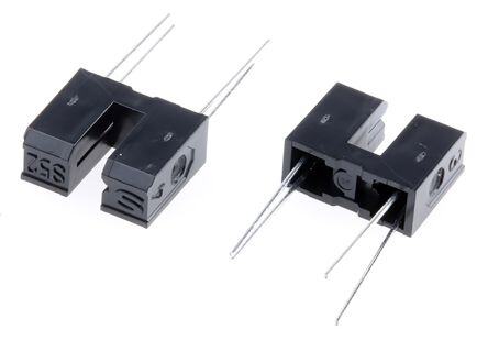
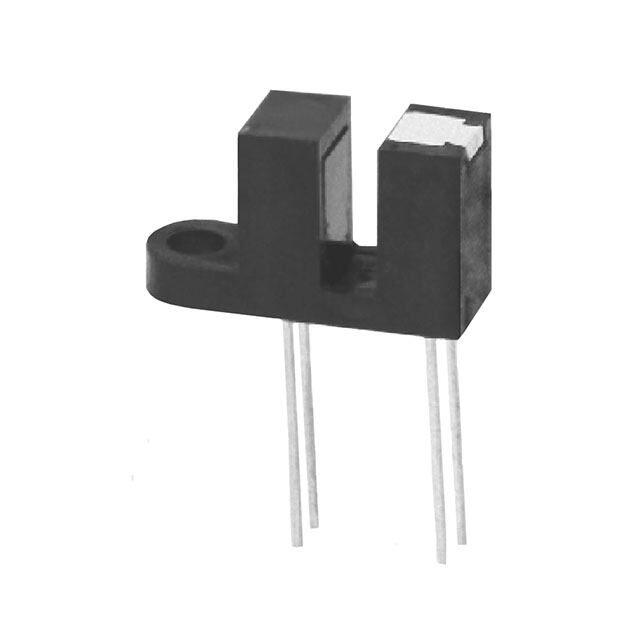
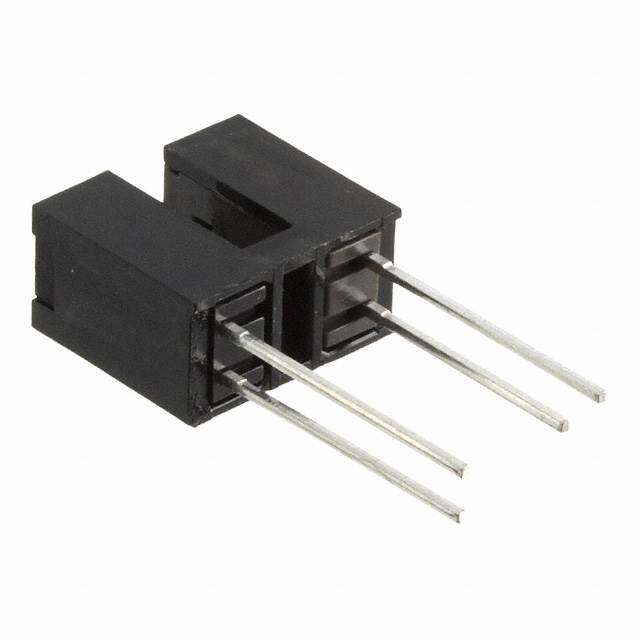
GP1S52VJ000F 是由 SHARP(现为 Socle Technology)生产的一款槽型光学传感器(光断续器),采用晶体管输出形式。该传感器广泛应用于需要非接触式检测物体位置、运动或存在与否的场景,尤其适用于空间受限、要求高精度检测的设备中。

其典型应用场景包括:

1. 办公设备:如打印机、扫描仪、复印机中,用于检测纸张是否到位、卡纸检测、盖板开合状态检测等;
2. 家电产品:如洗衣机、微波炉、电饭煲等,用于检测门是否关闭、内部组件位置状态等;
3. 工业自动化设备:用于自动化产线中的物料检测、位置定位、计数等功能;
4. 电子玩具与消费电子产品:用于检测运动部件位置或用户操作动作;
5. 医疗设备:如血糖仪、便携式监测设备中,用于检测试纸插入或部件状态;
6. 安防设备:用于门禁系统、摄像头云台限位检测等。

该传感器具有响应速度快、寿命长、抗干扰能力强等特点,适合在低电流、低电压环境下稳定工作,是众多电子产品中实现精确检测的理想选择。
| 参数 | 数值 |
| 产品目录 | |
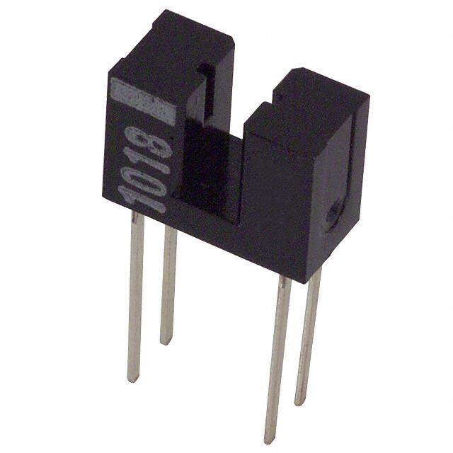
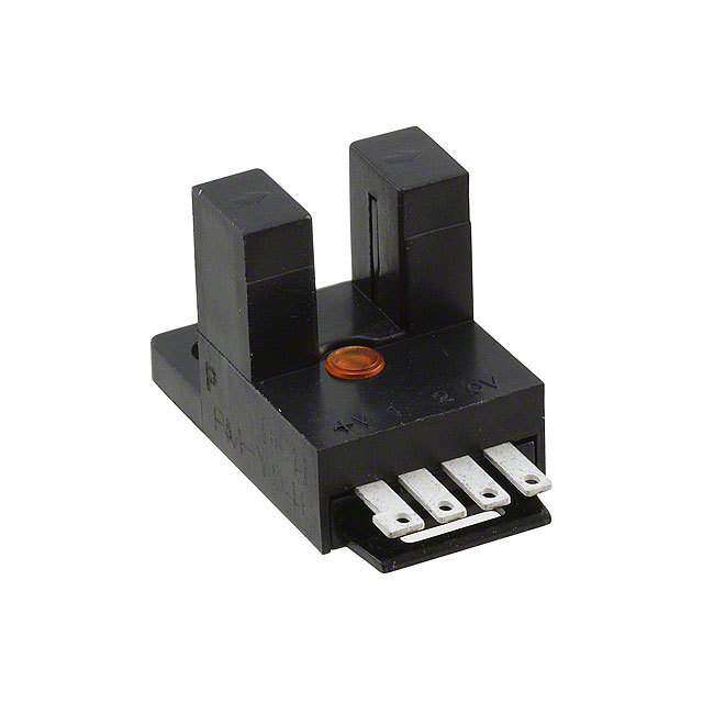
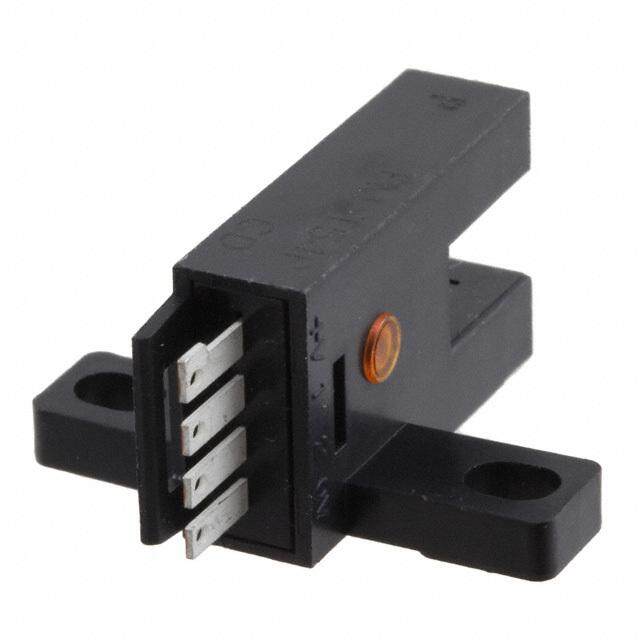
| 描述 | SENSOR OPTO SLOT 3MM TRANS THRU |
| 产品分类 | |
| 品牌 | Sharp Microelectronics |
| 数据手册 | http://www.sharpsma.com/webfm_send/1284 |
| 产品图片 |
|
| 产品型号 | GP1S52VJ000F |
| rohs | 无铅 / 符合限制有害物质指令(RoHS)规范要求 |
| 产品系列 | - |
| 产品目录页面 | |
| 其它名称 | 425-1971-5 |
| 包装 | 管件 |
| 响应时间 | 3µs, 4µs |
| 安装类型 | 通孔 |
| 封装/外壳 | PCB 安装 |
| 工作温度 | -25°C ~ 85°C |
| 感应方法 | 可传导的 |
| 感应距离 | 0.118"(3mm) |
| 标准包装 | 100 |
| 电压-集射极击穿(最大值) | 35V |
| 电流-DC正向(If) | 50mA |
| 电流-集电极(Ic)(最大值) | 20mA |
| 类型 | 无放大 |
| 输出配置 | 光电晶体管 |


- 商务部:美国ITC正式对集成电路等产品启动337调查
- 曝三星4nm工艺存在良率问题 高通将骁龙8 Gen1或转产台积电
- 太阳诱电将投资9.5亿元在常州建新厂生产MLCC 预计2023年完工
- 英特尔发布欧洲新工厂建设计划 深化IDM 2.0 战略
- 台积电先进制程称霸业界 有大客户加持明年业绩稳了
- 达到5530亿美元!SIA预计今年全球半导体销售额将创下新高
- 英特尔拟将自动驾驶子公司Mobileye上市 估值或超500亿美元
- 三星加码芯片和SET,合并消费电子和移动部门,撤换高东真等 CEO
- 三星电子宣布重大人事变动 还合并消费电子和移动部门
- 海关总署:前11个月进口集成电路产品价值2.52万亿元 增长14.8%
PDF Datasheet 数据手册内容提取
GP1S52VJ000F GP1S52VJ000F Gap : 3mm Slit : 0.5mm Phototransistor Output, Case package Transmissive Photointerrupter ■Description ■Agency approvals/Compliance GP1S52VJ000F is a standard, phototransistor output, 1. Compliant with RoHS directive transmissive photointerrupter with opposing emitter and detector in a case, providing non-contact sensing. For ■Applications this family of devices, the emitter and detector are insert- 1. General purpose detection of object presence or mo- ed in a case, resulting in a through-hole design. tion. 2. Example : Printer, FAX, Optical storage unit ■Features 1. Transmissive with phototransistor output 2. Highlights : • Verical Slit for alternate motion detection 3. Key Parameters : • Gap Width : 3mm • Slit Width (detector side): 0.5mm • Package : 12.2×10×5mm 4. RoHS directive compliant Notice The content of data sheet is subject to change without prior notice. In the absence of confi rmation by device specifi cation sheets, SHARP takes no responsibility for any defects that may occur in equipment using any SHARP devices shown in catalogs, data books, etc. Contact SHARP in order to obtain the latest device specifi cation sheets before using any SHARP device. Sheet No.: D3-A02501FEN 1 Date Oct. 3. 2005 © SHARP Corporation
GP1S52VJ000F ■Internal Connection Diagram Top view 3 2 1 Anode 2 Cathode 3 Collector 4 Emitter 4 1 ■Outline Dimensions (Unit : mm) Top view 12.2+−00..33 3+−00..21 Model No.25S 5 Sharp mark “S” A-Aʼ B-Bʼ section section 5 0.5 A B 2.5) enter) 0.5 1.5 C1 ( c or 5 ct Date code 5 10 7. Det mark (Both side) 3. ( 5 Aʼ Bʼ N. 2. MI 4−0.4+−00..31 10 4−0.45+−00..31 (9.2) (2.54) 4 1 3 2 • Unspecifi ed tolerance shall be as follows ; Dimension (d) Tolerance d≤6 ±0.1 6<d≤18 ±0.2 • ( ) : Reference dimensions Product mass : approx. 0.49g Dip soldering material : Sn−3Ag−0.5Cu Sheet No.: D3-A02501FEN 2
GP1S52VJ000F Date code (2 digit) 1st digit 2nd digit Year of production Month of production A.D. Mark Month Mark 2000 0 1 1 2001 1 2 2 2002 2 3 3 2003 3 4 4 2004 4 5 5 2005 5 6 6 2006 6 7 7 2007 7 8 8 2008 8 9 9 2009 9 10 X 2010 0 11 Y : : 12 Z repeats in a 10 year cycle Country of origin Japan, Indonesia or Philippines (Indicated on the packing case) Sheet No.: D3-A02501FEN 3
GP1S52VJ000F ■Absolute Maximum Ratings (Ta=25˚C) Parameter Symbol Rating Unit ∗1 Forward current I 50 mA F ∗1, 2Peak forward current I 1 A Input FM Reverse voltage V 6 V R Power dissipation P 75 mW Collector-emitter voltage V 35 V CEO Emitter-collector voltage V 6 V Output ECO Collector current I 20 mA C ∗1 Collector power dissipation P 75 mW C Operating temperature Topr −25 to +85 ˚C Storage temperature Tstg −40 to +100 ˚C ∗3Soldering temperature T 260 ˚C sol ∗1 Refer to Fig. 1, 2, 3 ∗2 Pulse width ≤ 100μs, Duty ratio=0.01 ∗3 For 5s or less ■Electro-optical Characteristics (Ta=25˚C) Parameter Symbol Condition MIN. TYP. MAX. Unit Forward voltage VF IF=20mA − 1.25 1.4 V Input Peak forward voltage VFM IFM=0.5A 3 4 V Reverse current IR VR=3V − − 10 μA Output Collector dark current ICEO VCE=20V − 1 100 nA Transfer Collector current IC VCE=5V, IF=20mA 0.5 − 5 mA charac- Collector-emitter saturation voltage VCE(sat) IF=40mA, IC=0.5mA − − 0.4 V teristics Response time RFaislle ttiimmee ttrf VCE=2V, IC=2mA, RL=100Ω −− 43 2105 μs Sheet No.: D3-A02501FEN 4
GP1S52VJ000F Fig.1 Forward Current vs. Ambient Fig.2 Collector Power Dissipation vs. Temperature Ambient Temperature 60 120 50 W) 100 m A) (C nt I (mF 40 pation P 8705 urre 30 dissi 60 d c er Forwar 20 or pow 40 ct e 10 oll 20 C 15 0 0 −25 0 25 50 75 85 100 −25 0 25 50 75 85 100 Ambient temperature Ta (˚C) Ambient temperature Ta (˚C) Fig.3 Peak Forward Current vs. Fig.4 Forward Current vs. Duty Ratio Forward Voltage Pulse width≤100μs Ta=25˚C Ta=75˚C 25˚C 0˚C A)1 000 50˚C −25˚C (mM mA) 100 d current IF current I (F war 100 ard 10 k for Forw a e P 10 1 10−2 10−1 1 0 0.5 1 1.5 2 2.5 3 3.5 Duty ratio Foward voltage VF (V) Fig.5 Collector Current vs. Fig.6 Collector Current vs. Forward Current Collector-emitter Voltage 12 7 TVaC=E2=55˚VC 6 Ta=25˚C 10 IF=50mA A) A) 5 m 8 m 40mA Collector current I (C 64 Collector current I (C 342 2300mmAA 2 10mA 1 0 0 0 10 20 30 40 50 0 1 2 3 4 5 6 7 8 9 10 Forward current IF (mA) Collector-emitter V (V) CE Sheet No.: D3-A02501FEN 5
GP1S52VJ000F Fig.7 Collector Current vs. Fig.8 Collector-emitter Saturation Voltage Ambient Temperature vs. Ambient Temperature 4 0.25 IVF=CE2=05mVA (V)E (sat) 0.2 IIFC==400.5mmAA C A) 3 e V m ag ector current I (C 2 er saturation volt 0.01.51 Coll 1 mitt e or- 0.05 ct e oll C 0 0 −25 0 25 50 75 100 −25 0 25 50 75 100 Ambient temperature Ta (˚C) Ambient temperature Ta (˚C) Fig.9 Response Time vs. Load Resistance Fig.10 Test Circuit for Response Time 100 VCE=2V IC=2mA Ta=25˚C VCC Input RD RL Input Output Output 10% s)μ 10 90% me ( tf onse ti td tr td tr ts tf p s Re 1 t s 0.1 0.01 0.1 1 10 Load resistance RL (kΩ) Fig.11 Frequency Response Fig.12 Collector Dark Current vs. Ambient Temperature 5 10−6 IVCC=E2=m2AV VCE=20V Ta=25˚C 0 A) (O 10−7 B) CE gain A (dV −5 RL= 1kΩ 100Ω k current I 10−8 ge −10 10kΩ dar Volta ctor e oll 10−9 −15 C −20 10−10 102 103 104 105 106 −25 0 25 50 75 100 Frequency f (Hz) Ambient temperature Ta (˚C) Sheet No.: D3-A02501FEN 6
GP1S52VJ000F Fig.13 Detecting Position Characteristics (1) Fig.14 Detecting Position Characteristics (2) IF=20mA, VCE=5V IF=20mA, VCE=5V Ta=25˚C Ta=25˚C 100 L 100 Shield %) %) nt ( Sensor nt ( L − e e 0 curr Shield curr + or or ct − + ct Sensor olle 50 0 olle 50 c c e e v v ati ati el el R R 0 0 −1.5 −1 −0.5 0 0.5 1 1.5 2 2.5 −3 −2 −1 0 1 2 3 4 5 Shield moving distance L (mm) Shield moving distance L (mm) Remarks : Please be aware that all data in the graph are just for reference and not for guarantee. Sheet No.: D3-A02501FEN 7
GP1S52VJ000F ■Design Considerations ●Design guide 1) Prevention of detection error To prevent photointerrupter from faulty operation caused by external light, do not set the detecting face to the external light. 2) Position of opaque board Opaque board shall be installed at place 4mm or more from the top of elements. (Example) 4mm or more This product is not designed against irradiation and incorporates non-coherent IRED. ●Degradation In general, the emission of the IRED used in photocouplers will degrade over time. In the case of long term operation, please take the general IRED degradation (50% degradation over 5 years) into the design consideration. ●Parts This product is assembled using the below parts. • Photodetector (qty. : 1) Maximum Sensitivity Sensitivity Category Material Response time (μs) wavelength (nm) wavelength (nm) Phototransistor Silicon (Si) 800 400 to 1 200 3 • Photo emitter (qty. : 1) Maximum light emitting Category Material I/O Frequency (MHz) wavelength (nm) Infrared emitting diode Gallium arsenide (GaAs) 950 0.3 (non-coherent) • Material Case Lead frame plating Black NORYL resin Solder dip. (Sn−3Ag−0.5Cu) Sheet No.: D3-A02501FEN 8
GP1S52VJ000F ■Manufacturing Guidelines ●Soldering Method Flow Soldering: Soldering should be completed below 260˚C and within 5 s. Please take care not to let any external force exert on lead pins. Please don't do soldering with preheating, and please don't do soldering by refl ow. Hand soldering Hand soldering should be completed within 3 s when the point of solder iron is below 350̊C. Please solder within one time. Please don't touch the terminals directly by soldering iron. Soldered product shall treat at normal temperature. Other notice Please test the soldering method in actual condition and make sure the soldering works fine, since the impact on the junction between the device and PCB varies depending on the cooling and soldering conditions. Flux Some fl ux, which is used in soldering, may crack the package due to synergistic effect of alcohol in fl ux and the rise in temperature by heat in soldering. Therefore, in using fl ux, please make sure that it does not have any infl uence on appearance and reliability of the photointerrupter. Sheet No.: D3-A02501FEN 9
GP1S52VJ000F ●Cleaning instructions Solvent cleaning : Solvent temperature should be 45˚C or below. Immersion time should be 3 minutes or less. Ultrasonic cleaning : The affect to device by ultrasonic cleaning is different by cleaning bath size, ultrasonic power output, cleaning time, PCB size or device mounting condition etc. Please test it in actual using condition and confi rm that doesn't occur any defect before starting the ultrasonic cleaning. Recommended solvent materials : Ethyl alcohol, Methyl alcohol and Isopropyl alcohol. ●Presence of ODC This product shall not contain the following materials. And they are not used in the production process for this product. Regulation substances : CFCs, Halon, Carbon tetrachloride, 1.1.1-Trichloroethane (Methylchloroform) Specifi c brominated fl ame retardants such as the PBBOs and PBBs are not used in this product at all. This product shall not contain the following materials banned in the RoHS Directive (2002/95/EC). •Lead, Mercury, Cadmium, Hexavalent chromium, Polybrominated biphenyls (PBB), Polybrominated diphenyl ethers (PBDE). Sheet No.: D3-A02501FEN 10
GP1S52VJ000F ■Package specifi cation ●Case package Package materials Anti-static plastic bag : Polyethtylene Moltopren : Urethane Partition : Corrugated fi berboard Packing case : Corrugated fi berboard Package method 100 pcs of products shall be packaged in a plastic bag, Ends shall be fi xed by stoppers. The bottom ot the packing case is covered with moltopren, and the partition is set in the packing case. Each partition should have 1 plastic bag. The 10 plastic bags containing a product are put in the packing case. Moltopren should be located after all product are settled (1 packing contains 1 000 pcs). Packing composition Moltopren Partition Anti-static plastic bag Packing case Sheet No.: D3-A02501FEN 11
GP1S52VJ000F ■Important Notices · The circuit application examples in this publication with equipment that requires higher reliability such as: are provided to explain representative applications of --- Transportation control and safety equipment (i.e., SHARP devices and are not intended to guarantee any aircraft, trains, automobiles, etc.) circuit design or license any intellectual property rights. --- Traffi c signals SHARP takes no responsibility for any problems related --- Gas leakage sensor breakers to any intellectual property right of a third party resulting --- Alarm equipment from the use of SHARP's devices. --- Various safety devices, etc. (iii) SHARP devices shall not be used for or in · Contact SHARP in order to obtain the latest device connection with equipment that requires an extremely specification sheets before using any SHARP device. high level of reliability and safety such as: SHARP reserves the right to make changes in the --- Space applications specifi cations, characteristics, data, materials, structure, --- Telecommunication equipment [trunk lines] and other contents described herein at any time --- Nuclear power control equipment without notice in order to improve design or reliability. --- Medical and other life support equipment (e.g., Manufacturing locations are also subject to change scuba). without notice. · If the SHARP devices listed in this publication fall · Observe the following points when using any devices within the scope of strategic products described in the in this publication. SHARP takes no responsibility for Foreign Exchange and Foreign Trade Law of Japan, it damage caused by improper use of the devices which is necessary to obtain approval to export such SHARP does not meet the conditions and absolute maximum devices. ratings to be used specifi ed in the relevant specifi cation sheet nor meet the following conditions: · This publication is the proprietary product of SHARP (i) The devices in this publication are designed for use and is copyrighted, with all rights reserved. Under in general electronic equipment designs such as: the copyright laws, no part of this publication may be --- Personal computers reproduced or transmitted in any form or by any means, --- Offi ce automation equipment electronic or mechanical, for any purpose, in whole or in --- Telecommunication equipment [terminal] part, without the express written permission of SHARP. --- Test and measurement equipment Express written permission is also required before any --- Industrial control use of this publication may be made by a third party. --- Audio visual equipment --- Consumer electronics · Contact and consult with a SHARP representative (ii) Measures such as fail-safe function and redundant if there are any questions about the contents of this design should be taken to ensure reliability and safety publication. when SHARP devices are used for or in connection [H150] Sheet No.: D3-A02501FEN 12
Mouser Electronics Authorized Distributor Click to View Pricing, Inventory, Delivery & Lifecycle Information: S harp Microelectronics: GP1S52VJ000F