 Datasheet下载
- 型号: GA342DR7GF331KW02L
- 制造商: Murata
- 库位|库存: xxxx|xxxx
- 要求:
| 数量阶梯 | 香港交货 | 国内含税 |
| +xxxx | $xxxx | ¥xxxx |
查看当月历史价格
查看今年历史价格
GA342DR7GF331KW02L产品简介:
ICGOO电子元器件商城为您提供GA342DR7GF331KW02L由Murata设计生产,在icgoo商城现货销售,并且可以通过原厂、代理商等渠道进行代购。 GA342DR7GF331KW02L价格参考¥4.33-¥4.33。MurataGA342DR7GF331KW02L封装/规格:陶瓷电容器, 330pF ±10% 250V 陶瓷电容器 X7R 1808(4520 公制)。您可以下载GA342DR7GF331KW02L参考资料、Datasheet数据手册功能说明书,资料中有GA342DR7GF331KW02L 详细功能的应用电路图电压和使用方法及教程。
Murata Electronics North America生产的陶瓷电容器型号GA342DR7GF331KW02L,属于高可靠性、高性能的多层陶瓷电容器(MLCC),广泛应用于需要稳定性和高频性能的场景。以下是该型号的主要应用场景:

 1. 电源管理
   - 用于开关电源(SMPS)、DC-DC转换器和电压调节模块(VRM)中的滤波和去耦。
   - 提供稳定的电容值以减少电源噪声,确保电路在高频下的正常运行。

 2. 射频和无线通信
   - 应用于射频前端模块(RF FEM)、滤波器和匹配网络中。
   - 支持5G基站、Wi-Fi模块和其他无线通信设备中的信号处理。

 3. 汽车电子
   - 适用于汽车电子控制单元(ECU)、ADAS(高级驾驶辅助系统)和车载信息娱乐系统。
   - 在高温、振动等恶劣环境下保持可靠性能。

 4. 工业自动化
   - 用于工业级变频器、伺服驱动器和PLC(可编程逻辑控制器)中的信号调理和滤波。
   - 提高设备在复杂电磁环境中的抗干扰能力。

 5. 消费类电子产品
   - 应用于智能手机、平板电脑和笔记本电脑的电源管理和信号传输部分。
   - 提供小型化设计和高容量特性,满足便携式设备的需求。

 6. 航空航天与国防
   - 由于其高可靠性和抗辐射特性,可用于卫星、雷达和军用通信设备。
   - 确保在极端条件下的长期稳定性。

 特性总结
- 高Q值:适合高频应用,降低信号损耗。
- 低ESR(等效串联电阻):提高效率,减少发热。
- 宽温度范围:适应各种工作环境。
- 小尺寸和高容量:支持紧凑型设计。

综上,GA342DR7GF331KW02L凭借其优异的性能参数,适用于对可靠性、频率响应和环境适应性要求较高的多种领域。
| 参数 | 数值 |
| 产品目录 | |
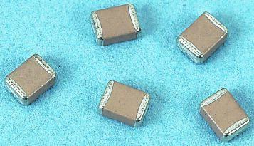
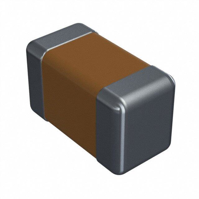
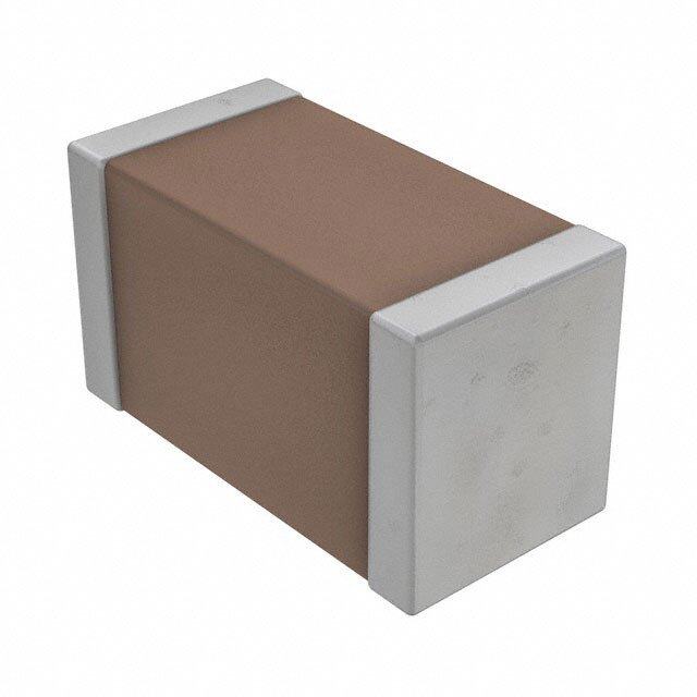
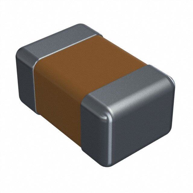
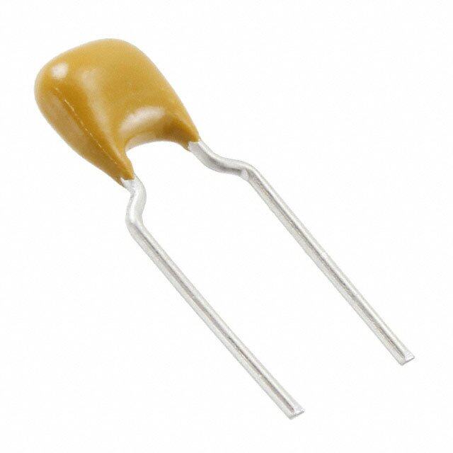
| 描述 | CAP CER 330PF 250VAC X7R 1808多层陶瓷电容器MLCC - SMD/SMT 1808 330pF 250Vac X7R 10% |
| 产品分类 | |
| 品牌 | Murata Electronics |
| 产品手册 | |
| 产品图片 |
|
| rohs | 符合RoHS无铅 / 符合限制有害物质指令(RoHS)规范要求 |
| 产品系列 | MLCC,多层陶瓷电容器MLCC - SMD/SMT,Murata Electronics GA342DR7GF331KW02LGA3 |
| 数据手册 | 点击此处下载产品Datasheet点击此处下载产品Datasheet点击此处下载产品Datasheet点击此处下载产品Datasheet点击此处下载产品Datasheet |
| 产品型号 | GA342DR7GF331KW02L |
| 产品 | Safety Certified MLCCs |
| 产品目录绘图 |
|
| 产品目录页面 | |
| 产品种类 | 多层陶瓷电容器MLCC - SMD/SMT |
| 其它名称 | 490-3474-1 |
| 包装 | 剪切带 (CT) |
| 厚度(最大值) | 0.087"(2.20mm) |
| 商标 | Murata Electronics |
| 外壳代码-in | 1808 |
| 外壳代码-mm | 4520 |
| 外壳宽度 | 2 mm |
| 外壳长度 | 4.5 mm |
| 外壳高度 | 2 mm |
| 大小/尺寸 | 0.177" 长 x 0.079" 宽(4.50mm x 2.00mm) |
| 安装类型 | 表面贴装,MLCC |
| 容差 | 10 % |
| 封装 | Reel |
| 封装/外壳 | 1808(4520 公制) |
| 封装/箱体 | 1808 (4520 metric) |
| 工作温度 | -55°C ~ 125°C |
| 工作温度范围 | - 55 C to + 125 C |
| 工厂包装数量 | 2000 |
| 应用 | 安全 |
| 引线形式 | - |
| 引线间距 | - |
| 最大工作温度 | + 125 C |
| 最小工作温度 | - 55 C |
| 标准包装 | 1 |
| 温度系数 | X7R |
| 温度系数/代码 | +/- 15 % |
| 特性 | - |
| 特色产品 | http://www.digikey.com/cn/zh/ph/Murata/GA3.html |
| 电介质 | X7R |
| 电压-额定 | 250VAC |
| 电压额定值 | 250 VAC |
| 电压额定值AC | 250 V |
| 电容 | 330 pF |
| 端接类型 | SMD/SMT |
| 等级 | X1Y2 |
| 类型 | Safety Standard Certified Class X1/Y2 |
| 系列 | GA3 |
| 高度-安装(最大值) | - |

%2022.jpg)


- 商务部:美国ITC正式对集成电路等产品启动337调查
- 曝三星4nm工艺存在良率问题 高通将骁龙8 Gen1或转产台积电
- 太阳诱电将投资9.5亿元在常州建新厂生产MLCC 预计2023年完工
- 英特尔发布欧洲新工厂建设计划 深化IDM 2.0 战略
- 台积电先进制程称霸业界 有大客户加持明年业绩稳了
- 达到5530亿美元!SIA预计今年全球半导体销售额将创下新高
- 英特尔拟将自动驾驶子公司Mobileye上市 估值或超500亿美元
- 三星加码芯片和SET,合并消费电子和移动部门,撤换高东真等 CEO
- 三星电子宣布重大人事变动 还合并消费电子和移动部门
- 海关总署:前11个月进口集成电路产品价值2.52万亿元 增长14.8%


PDF Datasheet 数据手册内容提取
C02E.pdf Nov.27,2017 Chip Multilayer Ceramic Capacitors for General 2018
!Note • Please read rating and !CAUTION (for storage, operating, rating, soldering, mounting and handling) in this catalog to prevent smoking and/or burning, etc. C02E.pdf • This catalog has only typical specifications. Therefore, please approve our product specifications or transact the approval sheet for product specifications before ordering. Nov.27,2017 M R Safety Standard Certified Chip Multilayer Ceramic Capacitors for General Purpose / IEC60384-14 Class X2 G GA3 Series Type GB WEB 3 R G J IEC60384-14 X2 Class Certified Product R G 4 R G Features 7 1 International Standard (IEC60384-14) certified product. R G Please down load Safety Standard Certification (Type GB: X2) from here. WEB M J G 2 Can be used as a Class X2 capacitor. M oSwitching Power Supply - Class 1 Equipment Q G C10 2 A G C8 C9 C3 C1 A3GB G C2 C6 C7 Controller A3GD G C5 C4 A3GF Recommend G No. Application MLCC Type C1 X Cap Type: GB L L C2 L C3 Y Cap Type: GF A C4 L L C5 Primary - Secondary Coupling Type: GF×2 M L L oSwitching Power Supply - Class 2 Equipment C9 LR L C3 C7 M C3 C8 NF C1 C2 C2 C5 C6 M Controller R K C4 3 R K Recommend No. Application MLCC Type MA G C1 X Cap Type: GB C2 Y Cap D M C3 Type: GF×2 G C4 Primary - Secondary Coupling Caution/Notice ! 189
!Note • Please read rating and !CAUTION (for storage, operating, rating, soldering, mounting and handling) in this catalog to prevent smoking and/or burning, etc. C02E.pdf • This catalog has only typical specifications. Therefore, please approve our product specifications or transact the approval sheet for product specifications before ordering. Nov.27,2017 M R G 3 Realized large capacitance value and small size while maintaining high withstand voltages by the multilayer structure. 3 R G Internal Electrodes Ceramic J R G Ni/Sn Plated Layer Foundation Electrode Layer 4 R G <Example of Structure> 7 R 4 Compared with conventional lead type capacitors, this product realized great reductions in size and G height, with a volume of 1/10 or less, and height of 1/4 or less. M J G 5 This product is only for reflow soldering. M Q G Specifications 2 A G e g e Size (mm) 5.7×5.0mm 3 GAGB Rated Voltage 250Vac T 3 Capacitance 10000pF to 56000pF GAGD L W Main Applications AC-DC power supply <Dimensions> 3 This catalog contains only a portion of the product lineup. A GGF Please refer to the capacitor search tool on the Murata Web site for details. L L L A L L M L L R L L M F N M R K 3 R K A M G D M G n o Cautiotice !N / 190
!Note • Please read rating and !CAUTION (for storage, operating, rating, soldering, mounting and handling) in this catalog to prevent smoking and/or burning, etc. C02E.pdf • This catalog has only typical specifications. Therefore, please approve our product specifications or transact the approval sheet for product specifications before ordering. Nov.27,2017 M GA3 Series Type GB High Dielectric Constant Type Part Number List R G 3 R 5.7×5.0mm G T Rated TC Cap. Tol. Part Number p* J max. Voltage Code R G 1.5mm 250Vac X7R 10000pF ±10% GA355QR7GB103KW01#p192 15000pF ±10% GA355QR7GB153KW01#p192 4 R 2.0mm 250Vac X7R 22000pF ±10% GA355DR7GB223KW01#p192 G 2.5mm 250Vac X7R 33000pF ±10% GA355ER7GB333KW01# p192 47000pF ±10% GA355ER7GB473KW01# p192 7 R G 2.9mm 250Vac X7R 56000pF ±10% GA355XR7GB563KW06#p192 M J G M Q G 2 A G A3GB G A3GD G A3GF G L L L A L L M L L R L L M F N M R K 3 R K A M G D M G Caution/Notice ! *: Refers to the page of the “Specifications and Test Methods”. Part number # indicates the package specification code. 191
!Note • Please read rating and !CAUTION (for storage, operating, rating, soldering, mounting and handling) in this catalog to prevent smoking and/or burning, etc. C02E.pdf • This catalog has only typical specifications. Therefore, please approve our product specifications or transact the approval sheet for product specifications before ordering. Nov.27,2017 M 1 GA3 Series Type GB Specifications and Test Methods (1) R G 3 GR No Item Specification Test Method (Ref. Standard: JIS C 5101, IEC60384) 1 Appearance No defects or abnormalities. Visual inspection. RJ 2 Dimension Within the specified dimensions. Using calipers and micrometers. G Measurement Point: Between the terminations Test Voltage: DC1075V 3 Voltage Proof No defects or abnormalities. 4 Applied Time: 60±1s R G Charge/discharge current: 50mA max. Measurement Point: Between the terminations Measurement Voltage: DC500±50V 7 4 Insulation Resistance (I.R.) 6000MΩ or more R Charging Time: 60±5s G Measurement Temperature: Room Temperature 5 Capacitance Shown in Rated value. Measurement Temperature: Room Temperature M Measurement Frequency: 1.0±0.1kHz J G 6 Dissipation Factor (D.F.) 0.025 max. Measurement Voltage: AC1.0±0.2V (r.m.s.) The capacitance change should be measured after 5 minutes at M each specified temp. stage. Q G Capacitance value as a reference is the value in step 3. Step Temperature (°C) A2 Temperature 12 MiRn.e Ofepreernactein Tge Tmepm. p±.2 ±3 G 7 Characteristics R7: Within ±15% (-55 to +125°C) 3 Reference Temp. ±2 of Capacitance 4 Max. Operating Temp. ±3 3 GAGB 5 Reference Temp. ±2 • Pretreatment Perform a heat treatment at 150+0/-10°C for 1h±5min and GA3GD Appearance No defects or abnormalities. Sthoeldne lre tt hseit cfaopr a2c4it±o2rh o. na tt hroeo tmes ct osnudbisttiorant*e. A shown in “Complement of Test Method”. Capacitance Within the specified initial value. 3 Kind of Vibration: A simple harmonic motion A GGF 8 Vibration 10Hz to 55Hz to 10Hz (1min) Total amplitude: 1.5mm D.F. Within the specified initial value. This motion should be applied for a period of 2h in each 3 mutually perpendicular directions (total of 6h). L L L Test Method: Solder bath method Flux: Solution of rosin ethanol 25 (wt)% Preheat: 80 to 120°C for 10 to 30s A 9 Solderability 95% of the terminations is to be soldered evenly and Solder: Sn-3.0Ag-0.5Cu (Lead Free Solder) L continuously. L Solder Temp.: 245±5°C Immersion time: 2±0.5s Immersing in speed: 25±2.5mm/s. M LL Appearance No defects or abnormalities. Test Method: Solder bath method Solder: Sn-3.0Ag-0.5Cu (Lead Free Solder) Capacitance Within ±10% Solder Temp.: 260±5°C Change R Immersion time: 10±1s L Resistance L I.R. 1000MΩ or more Immersing in speed: 25±2.5mm/s. to 10 Exposure Time: 24±2h at room condition*. Soldering Preheat: GA355 size: 100 to 120°C for 1min and 170 to 200°C M Heat F Voltage for 1min N Proof No defects. • Pretreatment Perform a heat treatment at 150+0/-10°C for 1h±5min and M then let sit for 24±2h at room condition*. R K Solder the capacitor on the test substrate A shown in “Complement of Test Method”. KR3 11 Aofd Theersmivien aSttiroenngth Nococ ruerm. oval of the terminations or other defect should 10N, 10±1s Applied Direction: In parallel with the test substrate and vertical with the capacitor side. A M G Solder the capacitor on the test substrate B shown in “Complement of Test Method”. Then apply the force in the direction shown in “Test Method of MD 12 SBuebnsdtinragt Teest No defects or abnormalities. Substrate Bending Test” of “Complement of Test Method”. G Flexure: 1mm Holding Time: 5±1s n !CautioNotice * Room Condition: Temperature: 15 to 35°C, Relative humidity: 45 to 75%, Atmosphere presSsuorldee: 8ri6ng t oM 1e0th6okdP:a Reflow soldering / Continued on the following page. 192
!Note • Please read rating and !CAUTION (for storage, operating, rating, soldering, mounting and handling) in this catalog to prevent smoking and/or burning, etc. C02E.pdf • This catalog has only typical specifications. Therefore, please approve our product specifications or transact the approval sheet for product specifications before ordering. Nov.27,2017 GA3 Series Type GB Specifications and Test Methods (1) M R G Continued from the preceding page. 3 No Item Specification Test Method (Ref. Standard: JIS C 5101, IEC60384) GR Appearance No defects or abnormalities. Fix the capacitor to the supporting test substrate A (glass epoxy board) shown in “Complement of Test Method”. Capacitance Within±15% Perform the 5 cycles according to the four heat treatments RJ Change G shown in the following table. D.F. 0.05 max. Step Temp. (°C) Time (min) 4 Temperature I.R. 3000MΩ or more 1 Min. Operating Temp. +0/-3 30±3 R G 13 Sudden 2 Room Temp. 2 to 3 Change 3 Max. Operating Temp. +3/-0 30±3 4 Room Temp. 2 to 3 7 Voltage R No defects. Exposure Time: 24±2h at room condition*. G Proof • Pretreatment Perform a heat treatment at 150+0/-10°C for 1h±5min and M then let sit for 24±2h at room condition*. J G Appearance No defects or abnormalities. Fix the capacitor to the supporting test substrate B (glass epoxy board) shown in “Complement of Test Method”. Capacitance Within±15% Before this test, the test shown in the following is performed. M Change Q • No.11 Adhesive Strength of Termination (apply force: 5N) G High D.F. 0.05 max. • No.12 Substrate Bending Test Temperature Test Temperature: 40±2°C 14 High I.R. 3000MΩ or more Test Humidity: 90 to 95%RH A2 Humidity Test Time: 500+24/-0h G (Steady) Applied Voltage: Rated voltage VProoltoafge No defects. E• xPpreotsrueraet mTimenet: 24±2h at room condition*. A3GB G Perform a heat treatment at 150+0/-10°C for 1h±5min and then let sit for 24±2h at room condition*. Appearance No defects or abnormalities. Fix the capacitor to the supporting test substrate B (glass epoxy A3GD board) shown in “Complement of Test Method”. G Capacitance Within ±20% Before this test, the test shown in the following is performed. Change • No.11 Adhesive Strength of Termination (apply force: 5N) D.F. 0.05 max. • No.12 Substrate Bending Test A3GF Next, Impulse Voltage test is performed. G I.R. 3000MΩ or more Each individual capacitor shall be subjected to a 2.5kV Impulse (the voltage value means zero to peak) for 3 times. L Then the capacitors are applied to life test. L L 100 (%) 90 A 50 Front time (T1) = 1.2µs=1.67T LL 30 Time to half-value (T2) = 50µs 15 Durability 0 t T M T1 L L Voltage T2 No defects. Proof Apply voltage as Table for 1000h at 125+2/-0°C , relative humidity 50% max. R L L Applied Voltage AC312.5V (r.m.s.), except that once each hour the voltage is increased to AC1000V (r.m.s.) for 0.1s. M F N Exposure Time: 24±2h at room condition*. • Pretreatment Perform a heat treatment at 150+0/-10°C for 1h±5min and M then let sit for 24±2h at room condition*. R K * Room Condition: Temperature: 15 to 35°C, Relative humidity: 45 to 75%, Atmosphere pressure: 86 to 106kPa Continued on the following page. 3 R K A M G D M G Caution/Notice ! 193
!Note • Please read rating and !CAUTION (for storage, operating, rating, soldering, mounting and handling) in this catalog to prevent smoking and/or burning, etc. C02E.pdf • This catalog has only typical specifications. Therefore, please approve our product specifications or transact the approval sheet for product specifications before ordering. Nov.27,2017 M GA3 Series Type GB Specifications and Test Methods (1) R G Continued from the preceding page. 3 GR No Item Specification Test Method (Ref. Standard: JIS C 5101, IEC60384) The capacitor under test shall be held in the flame in the position which best promotes burning. J R Each specimen shall only be exposed once to the flame. G Time of exposure to flame: 30s Length of flame: 12±1mm 4 Gas burner: Length 35mm min. R G Inside dia: 0.5±0.1mm Outside dia: 0.9mm max. Gas: Butane gas purity 95% min. The burning time shall not be exceeded the time 30s. 7 16 Passive Flammability R The tissue paper shall not ignite. G Test Specimen Approximately 8mm M Buner Flame GJ 45° 200±5mm M Tissue Paper Q G Wood Board of Approximately 10mm in Thickness The specimens shall be individually wrapped in at least one but A2 more than two complete layers of cheesecloth. G The specimens shall be subjected to 20 discharges. The interval between successive discharges shall be 5s. 3 The UAC shall be maintained for 2min after the last discharge. GAGB S1 F L1 L2 R Ui S3 3 S2 C1 C2 C3 Cx Ct Ut GAGD U- L3 L4 Tr Oscilloscope 3 A GGF C1,C2: Filter capacitor 1µF±10% C3: Capacitor 0.033µF±5% 17 Active Flammability The cheesecloth shall not be on fire. L1 to L4: Rod coa choke 1.5mH±20%, 16A L R: Resistor 100Ω±2% Cx < 0.068µF LL Ct: Tank capacitor 3µF±5% 10kV Cx <= 1µF U-: UR±5% UR: Rated voltage A Cx: Capacitor under test L L F: Slow-blow fuse, rated 16A Ut: Voltage to which the tank capacitor Ct is charged M Ux L L 2.5kV R L L time M F N M R K 3 R K A M G D M G n o Cautiotice !N / 194
!Note • Please read rating and !CAUTION (for storage, operating, rating, soldering, mounting and handling) in this catalog to prevent smoking and/or burning, etc. C02E.pdf • This catalog has only typical specifications. Therefore, please approve our product specifications or transact the approval sheet for product specifications before ordering. Nov.27,2017 GA3 Series Type GB Specifications and Test Methods (1) M R G Continued from the preceding page. 3 Complement of Test Method R G 1. Test Substrate The test substrate should be Substrate A or Substrate B as described in “Specifications and Test Methods”. J The specimen should be soldered by the conditions as described below. GR Soldering Method: Reflow soldering Solder: Sn-3.0Ag-0.5Cu 4 R (1) Test Substrate A G • Land Dimensions Chip Capacitor Land Part Number a Dimensibon (mm) c GR7 GA355 4.5 8.0 5.6 c M a J Solder Resist G b • Material: Glass Epoxy Board M • Thickness: 1.6mm Q G • Thickness of Copper Foil: 0.035mm (2) Test Substrate B 2 A a Dimension of Pattern (mm) G Part Number a b c d 40 d c GA355 4.5 8.0 5.6 1.0 A3GB (ø4.5) G b 1.6 100 Copper Foil A3GD Solder Resist (in mm) G • Material: Glass Epoxy Board • Thickness of Copper Foil: 0.035mm A3GF G 2. Test Method of Substrate Bending Test (a) Support State (b) Test State Test Substrate B 20 Test Substrate B LL a L Capacitor Support Stand (ø5) min. b 50 A L L 45±2 45±2 Test Stand (in mm) Pressure Stick Support Stand (in mm) M a: ±2 gap between support stand center and test stand b: ±5 gap between support stand center and test stand center L L • Material of Test Stand and Pressure Stick The material shoud be a metal where a remarkable transformation and the distortion are not caused even if it is pressurized. R • Pressurizing Speed LL The pressurizing speed is pressurized at the speed of about 1mm/s until the flexure reaches a regulated value. Pressure Stick M F NF R5 L Support Stand M R K 3 R K A M G D M G Caution/Notice ! 195
!Note • Please read rating and !CAUTION (for storage, operating, rating, soldering, mounting and handling) in this catalog to prevent smoking and/or burning, etc. C02E.pdf • This catalog has only typical specifications. Therefore, please approve our product specifications or transact the approval sheet for product specifications before ordering. Nov.27,2017 M R G Safety Standard Certified Chip Multilayer Ceramic Capacitors for General Purpose / Acquired certifications of UL60950-1 GA3 Series Type GD 3 WEB R G J R UL60950-1 Certified Product G 4 R G Features 7 R 1 International Standard (IEC60384-14) certified product. G Please down load Safety Standard Certification (Type GD) from here. WEB M J G 2 Can be uesd for UL60950-1 devices. M Q oDAA Modem - Transformer Less G Tel Line 2 C1 C5 A G GA3GB C1 C5 No. Application RMeLcComC mTyepned Bus C5 Lighting Surge Absorption 3 GAGD C7 C2 C6 Noise Immunity Type: GD / GF C7 D/A Isolation Barrier 3 GAGF C3 C4 C6 L L L GND LA 3 Realized large capacitance value and small size while maintaining high withstand voltages by the L multilayer structure. M L Internal Electrodes L Ceramic R L Ni/Sn Plated Layer L Foundation Electrode Layer M F <Example of Structure> N 4 This product is only for reflow soldering. M R K Specifications 3 R K e g e Size (mm) 4.5×2.0mm to 4.5×3.2mm A M G Rated Voltage 250Vac T Capacitance 10pF to 4700pF D W M L G Main Applications Modem <Dimensions> n Cautiootice TPhleisa scea traelfoegr tcoo nthtaei ncsa poanclyit oa rp soeratirocnh otof othl eo np rtohdeu Mctu rlianteau Wp.eb site for details. !N / 196
!Note • Please read rating and !CAUTION (for storage, operating, rating, soldering, mounting and handling) in this catalog to prevent smoking and/or burning, etc. C02E.pdf • This catalog has only typical specifications. Therefore, please approve our product specifications or transact the approval sheet for product specifications before ordering. Nov.27,2017 M GA3 Series Type GD Temperature Compensating Type Part Number List R G 3 R 4.5×2.0mm G T Rated TC Cap. Tol. Part Number p* J max. Voltage Code R G 1.0mm 250Vac SL 10pF ±5% GA342A1XGD100JW31# p199 12pF ±5% GA342A1XGD120JW31# p199 4 R 15pF ±5% GA342A1XGD150JW31# p199 G 18pF ±5% GA342A1XGD180JW31# p199 22pF ±5% GA342A1XGD220JW31# p199 7 R G 27pF ±5% GA342A1XGD270JW31# p199 33pF ±5% GA342A1XGD330JW31# p199 M 39pF ±5% GA342A1XGD390JW31# p199 J G 47pF ±5% GA342A1XGD470JW31# p199 56pF ±5% GA342A1XGD560JW31# p199 M 68pF ±5% GA342A1XGD680JW31# p199 Q G 82pF ±5% GA342A1XGD820JW31# p199 2 A G A3GB G A3GD G A3GF G L L L A L L M L L R L L M F N M R K 3 R K A M G D M G Caution/Notice ! *: Refers to the page of the “Specifications and Test Methods”. Part number # indicates the package specification code. 197
!Note • Please read rating and !CAUTION (for storage, operating, rating, soldering, mounting and handling) in this catalog to prevent smoking and/or burning, etc. C02E.pdf • This catalog has only typical specifications. Therefore, please approve our product specifications or transact the approval sheet for product specifications before ordering. Nov.27,2017 M R GA3 Series Type GD High Dielectric Constant Type Part Number List G 3 R G 4.5×2.0mm T Rated TC J Cap. Tol. Part Number p* R max. Voltage Code G 1.5mm 250Vac X7R 100pF ±10% GA342QR7GD101KW01#p203 4 150pF ±10% GA342QR7GD151KW01#p203 R G 220pF ±10% GA342QR7GD221KW01#p203 330pF ±10% GA342QR7GD331KW01#p203 7 470pF ±10% GA342QR7GD471KW01#p203 R G 680pF ±10% GA342QR7GD681KW01#p203 1000pF ±10% GA342QR7GD102KW01#p203 M J 1500pF ±10% GA342QR7GD152KW01#p203 G M 4.5×3.2mm Q G T Rated TC Cap. Tol. Part Number p* max. Voltage Code 2 A G 1.5mm 250Vac X7R 1800pF ±10% GA343QR7GD182KW01#p203 2200pF ±10% GA343QR7GD222KW01#p203 3 GAGB 2.0mm 250Vac X7R 4700pF ±10% GA343DR7GD472KW01#p203 3 GAGD 3 A GGF L L L A L L M L L R L L M F N M R K 3 R K A M G D M G n o Cautiotice !N / 198 *: Refers to the page of the “Specifications and Test Methods”. Part number # indicates the package specification code.
!Note • Please read rating and !CAUTION (for storage, operating, rating, soldering, mounting and handling) in this catalog to prevent smoking and/or burning, etc. C02E.pdf • This catalog has only typical specifications. Therefore, please approve our product specifications or transact the approval sheet for product specifications before ordering. Nov.27,2017 1 GA3 Series Type GD Specifications and Test Methods (1) M R G 3 No Item Specification Test Method (Ref. Standard: JIS C 5101, IEC60384) GR 1 Appearance No defects or abnormalities. Visual inspection. 2 Dimension Within the specified dimensions. Using calipers and micrometers. RJ G Measurement Point: Between the terminations Test Voltage: AC1500V (r.m.s.) 3 Voltage Proof No defects or abnormalities. Applied Time: 60±1s 4 R Charge/discharge current: 50mA max. G 10 impulse of alternating polarity is subjected. (5 impulse for No self healing break downs or flash-overs have taken each polarity) 4 Impulse Voltage 7 place in the capacitor. The interval between impulse is 60s. R G Applied Voltage: 2.5kVo-p Measurement Point: Between the terminations M Measurement Voltage: DC500±50V 5 Insulation Resistance (I.R.) 6000MΩ or more Charging Time: 60±5s GJ Measurement Temperature: Room Temperature 6 Capacitance Shown in Rated value. M Measurement Temperature: Room Temperature Q C >= 30pF: 1000 or more Measurement Frequency: 1.0±0.1MHz G 7 Q C < 30pF: 400+20C or more Measurement Voltage: AC1.0±0.2V (r.m.s.) C: Nominal Capacitance (pF) 2 A The capacitance change should be measured after 5 minutes at G each specified temp. stage. Capacitance value as a reference is the value in step 3. A3GB Step Temperature (°C) G Temperature 1 Reference Temp. ±2 1X: +350 to -1000 ppm/°C 8 Characteristics 2 Min. Operating Temp. ±3 of Capacitance (Temp.Range:+20 to +85°C) 3 Reference Temp. ±2 A3GD 4 Max. Operating Temp. ±3 G 5 Reference Temp. ±2 However, the capacitance shall be measured at even 85°C A3GF between step 3 and step 4. G Appearance No defects or abnormalities. Solder the capacitor on the test substrate A shown in “Complement of Test Method”. Capacitance Within the specified initial value. L Kind of Vibration: A simple harmonic motion L L 9 Vibration 10Hz to 55Hz to 10Hz (1min) Total amplitude: 1.5mm Q Within the specified initial value. This motion should be applied for a period of 2h in each 3 A mutually perpendicular directions (total of 6h). LL Test Method: Solder bath method Flux: Solution of rosin ethanol 25 (wt)% M 10 Solderability 95% of the terminations is to be soldered evenly and PSoreldheera: tS: n8-03 .t0oA 1g2-00°.5CC fuo r( L1e0a dto F 3re0es Solder) LL continuously. Solder Temp.: 245±5°C Immersion time: 2±0.5s R Immersing in speed: 25±2.5mm/s. L L Appearance No defects or abnormalities. Test Method: Solder bath method Solder: Sn-3.0Ag-0.5Cu (Lead Free Solder) Capacitance M Resistance Change Within±2.5% or ±0.25pF (Whichever is larger) Solder Temp.: 260±5°C NF to Immersion time: 10±1s 11 Soldering I.R. 1000MΩ or more Immersing in speed: 25±2.5mm/s. Heat Exposure Time: 24±2h at room condition*. M VProoltoafge No defects. P reheat: GA342 size: 1an0d0 1to7 01 2to0 °2C0 0fo°rC 1 fmorin 1min KR Solder the capacitor on the test substrate A shown in “Complement of Test Method”. R3 K Adhesive Strength No removal of the terminations or other defect should 12 10N, 10±1s of Termination occur. A Applied Direction: In parallel with the test substrate and M G vertical with the capacitor side. Solder the capacitor on the test substrate B shown in D “Complement of Test Method”. M Then apply the force in the direction shown in “Test Method of G Substrate 13 No defects or abnormalities. Substrate Bending Test” of “Complement of Test Method”. Bending Test FHSlooellxddueinrreign: gT1 imMmmeet: h5o±d1:s Reflow soldering Caution/Notice ! * Room Condition: Temperature: 15 to 35°C, Relative humidity: 45 to 75%, Atmosphere pressure: 86 to 106kPa Continued on the following page. 199
!Note • Please read rating and !CAUTION (for storage, operating, rating, soldering, mounting and handling) in this catalog to prevent smoking and/or burning, etc. C02E.pdf • This catalog has only typical specifications. Therefore, please approve our product specifications or transact the approval sheet for product specifications before ordering. Nov.27,2017 M GA3 Series Type GD Specifications and Test Methods (1) R G Continued from the preceding page. 3 GR No Item Specification Test Method (Ref. Standard: JIS C 5101, IEC60384) Appearance No defects or abnormalities. Fix the capacitor to the supporting test substrate A (glass epoxy board) shown in “Complement of Test Method” RJ Capacitance Within ±2.5% or ±0.25pF (Whichever is larger) Perform the 5 cycles according to the four heat treatments G Change shown in the following table. Temperature Q Within the specified initial value. Step Temp. (°C) Time (min) 4 14 Sudden R I.R. 3000MΩ or more 1 Min. Operating Temp. +0/-3 30±3 G Change 2 Room Temp. 2 to 3 3 Max. Operating Temp. +3/-0 30±3 Voltage No defects. 4 Room Temp. 2 to 3 7 Proof R G Exposure Time: 24±2h at room condition*. Appearance No defects or abnormalities. Fix the capacitor to the supporting test substrate B (glass epoxy M Capacitance board) shown in “Complement of Test Method”. GJ Change Within ±5.0% or ±0.5pF (Whichever is larger) Before this test, the test shown in the following is performed. High • No.12 Adhesive Strength of Termination (apply force: 5N) Temperature C >= 30pF: 350 or more • No.13 Substrate Bending Test M 15 High Q C < 30pF: 275+5/2C or more Q Test Temperature: 40±2°C G Humidity C: Nominal Capacitance (pF) Test Humidity: 90 to 95%RH (Steady) I.R. 3000MΩ or more Test Time: 500+24/-0h. A2 Voltage No defects. AExpppoliseudr eV oTlitmagee:2: 4R±a2tehd a vt oroltoamge condition*. G Proof Appearance No defects or abnormalities. Fix the capacitor to the supporting test substrate B (glass epoxy 3 GAGB Capacitance Within ±3.0% or ±0.3pF (Whichever is larger) bBoeafordre) sthhiosw tens itn, “tCheo mtepslte smheonwtn o ifn T tehset fMolelothwoindg”. is performed. Change • No.12 Adhesive Strength of Termination (apply force: 5N) 3 C >= 30pF: 350 or more • No.13 Substrate Bending Test GAGD Q C < 30pF: 275+5/2C or more Next, Impulse Voltage test is performed. C: Nominal Capacitance (pF) Each individual capacitor shall be subjected to a 2.5kV Impulse (the voltage value means zero to peak) for 3 times. I.R. 3000MΩ or more 3 Then the capacitors are applied to life test. A GGF 100 (%) 90 16 Durability 50 Front time (T1) = 1.2µs=1.67T LL 30 Time to half-value (T2) = 50µs L 0 t T T1 LLA VProoltoafge No defects. T2 Apply voltage as Table for 1000h at 125+2/-0°C , relative humidity 50% max. M LL Applied voltage AC425V (r.m.s.), except that once each hour the voltage is increased to AC1000V (r.m.s.) for 0.1s. R Exposure Time: 24±2h at room condition*. L L The capacitor under test shall be held in the flame in the position which best promotes burning. M Each specimen shall only be exposed once to the flame. NF Time of exposure to flame: 30s Length of flame: 12±1mm Gas burner: Length 35mm min. M Inside dia: 0.5±0.1mm R K Outside dia: 0.9mm max. Gas: Butane gas purity 95% min. The burning time shall not be exceeded the time 30s. 17 Passive Flammability R3 The tissue paper shall not ignite. Test Specimen K Approximately 8mm Buner Flame MA 45° 200±5mm G Tissue Paper D M Wood Board of Approximately 10mm in Thickness G n * Room Condition: Temperature: 15 to 35°C, Relative humidity: 45 to 75%, Atmosphere pressure: 86 to 106kPa o Cautiotice Continued on the following page. !N / 200
!Note • Please read rating and !CAUTION (for storage, operating, rating, soldering, mounting and handling) in this catalog to prevent smoking and/or burning, etc. C02E.pdf • This catalog has only typical specifications. Therefore, please approve our product specifications or transact the approval sheet for product specifications before ordering. Nov.27,2017 GA3 Series Type GD Specifications and Test Methods (1) M R G Continued from the preceding page. 3 No Item Specification Test Method (Ref. Standard: JIS C 5101, IEC60384) GR The specimens shall be individually wrapped in at least one but more than two complete layers of cheesecloth. J The specimens shall be subjected to 20 discharges. R G The interval between successive discharges shall be 5s. The UAC shall be maintained for 2min after the last discharge. S1 F L1 L2 R R4 Ui G S3 S2 C1 C2 C3 Cx Ct Ut U- L3 L4 7 Tr R G Oscilloscope M C1, C2: Filter capacitor 1µF±10% J C3: Capacitor 0.033µF±5% G 18 Active Flammability The cheesecloth shall not be on fire. L1 to L4: Rod coa choke 1.5mH±20%, 16A R: Resistor 100Ω±2% Cx < 0.068µF M Ct: Tank capacitor 3µF±5% 10kV Cx <= 1µF Q U-: UR±5% G UR: Rated voltage Cx: Capacitor under test 2 F: Slow-blow fuse, rated 16A A G Ut: Voltage to which the tank capacitor Ct is charged Ux A3GB 2.5kV G A3GD G time A3GF G L L L A L L M L L R L L M F N M R K 3 R K A M G D M G Caution/Notice ! 201
!Note • Please read rating and !CAUTION (for storage, operating, rating, soldering, mounting and handling) in this catalog to prevent smoking and/or burning, etc. C02E.pdf • This catalog has only typical specifications. Therefore, please approve our product specifications or transact the approval sheet for product specifications before ordering. Nov.27,2017 M GA3 Series Type GD Specifications and Test Methods (1) R G Continued from the preceding page. 3 R Complement of Test Method G 1. Test Substrate J The test substrate should be Substrate A or Substrate B as described in “Specifications and Test Methods”. GR The specimen should be soldered by the conditions as described below. Soldering Method: Reflow soldering Solder: Sn-3.0Ag-0.5Cu 4 R G (1) Test Substrate A • Land Dimensions Chip Capacitor GR7 Land Part Number a Dimensibon (mm) c GA342 3.5 7.0 2.4 c M J a G Solder Resist b M • Material: Glass Epoxy Board Q • Thickness: 1.6mm G • Thickness of Copper Foil: 0.035mm 2 (2) Test Substrate B A G a Dimension of Pattern (mm) Part Number a b c d 3 d c GA342 3.5 7.0 2.4 1.0 GAGB 40 (ø4.5) b 1.6 3 GAGD 100 CSoolpdpeerr R Feosiilst (in mm) • Material: Glass Epoxy Board 3 • Thickness of Copper Foil: 0.035mm A GGF 2. Test Method of Substrate Bending Test (a) Support State (b) Test State LL Test Substrate B 20 Test Substrate B L a Capacitor Support Stand (ø5) min. b A 50 L L 45±2 45±2 Test Stand (in mm) Pressure Stick Support Stand (in mm) M L a: ±2 gap between support stand center and test stand b: ±5 gap between support stand center and test stand center L • Material of Test Stand and Pressure Stick The material shoud be a metal where a remarkable transformation and the distortion are not caused even if it is pressurized. R LL • Pressurizing Speed The pressurizing speed is pressurized at the speed of about 1mm/s until the flexure reaches a regulated value. M Pressure Stick NF F R5 L M Support Stand R K 3 R K A M G D M G n o Cautiotice !N / 202
!Note • Please read rating and !CAUTION (for storage, operating, rating, soldering, mounting and handling) in this catalog to prevent smoking and/or burning, etc. C02E.pdf • This catalog has only typical specifications. Therefore, please approve our product specifications or transact the approval sheet for product specifications before ordering. Nov.27,2017 2 GA3 Series Type GD Specifications and Test Methods (2) M R G 3 No Item Specification Test Method (Ref. Standard: JIS C 5101, IEC60384) GR 1 Appearance No defects or abnormalities. Visual inspection. 2 Dimension Within the specified dimensions. Using calipers and micrometers. RJ G Measurement Point: Between the terminations Test Voltage: AC1500V (r.m.s.) 3 Voltage Proof No defects or abnormalities. Applied Time: 60±1s 4 R Charge/discharge current: 50mA max. G 10 impulse of alternating polarity is subjected. (5 impulse for No self healing break downs or flash-overs have taken each polarity) 4 Impulse Voltage 7 place in the capacitor. The interval between impulse is 60s. R G Applied Voltage: 2.5kVo-p Measurement Point: Between the terminations M Measurement Voltage: DC500±50V 5 Insulation Resistance (I.R.) 6000MΩ or more Charging Time: 60±5s GJ Measurement Temperature: Room Temperature 6 Capacitance Shown in Rated value. Measurement Temperature: Room Temperature M Q Measurement Frequency: 1.0±0.1kHz G 7 Dissipation Factor (D.F.) 0.025 max. Measurement Voltage: AC1.0±0.2V (r.m.s.) The capacitance change should be measured after 5 minutes at 2 each specified temp. stage. A G Capacitance value as a reference is the value in step 3. St1ep RTeefemrepnecraet Tuerem (p°.C ±)2 A3GB Temperature G 2 Min. Operating Temp. ±3 8 Characteristics R7: Within ±15% (-55 to +125°C) 3 Reference Temp. ±2 of Capacitance 45 MaRxe. fOepreenractei nTge Tmepm. ±p2. ±3 A3GD G • Pretreatment Perform a heat treatment at 150+0/-10°C for 1h±5min and then let sit for 24±2h at room condition*. A3GF G Appearance No defects or abnormalities. Solder the capacitor on the test substrate A shown in “Complement of Test Method”. Capacitance Within the specified initial value. Kind of Vibration: A simple harmonic motion L L 9 Vibration 10Hz to 55Hz to 10Hz (1min) L Total amplitude: 1.5mm D.F. Within the specified initial value. This motion should be applied for a period of 2h in each 3 mutually perpendicular directions (total of 6h). A L L Test Method: Solder bath method Flux: Solution of rosin ethanol 25 (wt)% Preheat: 80 to 120°C for 10 to 30s M 10 Solderability 9co5n%ti nouf othuesl yte.rminations is to be soldered evenly and Solder: Sn-3.0Ag-0.5Cu (Lead Free Solder) LL Solder Temp.: 245±5°C Immersion time: 2±0.5s Immersing in speed: 25±2.5mm/s. R L L Appearance No defects or abnormalities. Test Method: Solder bath method Solder: Sn-3.0Ag-0.5Cu (Lead Free Solder) Capacitance Within ±10% Solder Temp.: 260±5°C M Resistance Change Immersion time: 10±1s NF I.R. 1000MΩ or more Immersing in speed: 25±2.5mm/s. to 11 Exposure Time: 24±2h at room condition*. Soldering Preheat: GA342/43 size: 100 to 120°C for 1min M Heat R Voltage and 170 to 200°C for 1min K Proof No defects. • Pretreatment Perform a heat treatment at 150+0/-10°C for 1h±5min and then let sit for 24±2h at room condition*. R3 K Solder the capacitor on the test substrate A shown in “Complement of Test Method”. A Adhesive Strength No removal of the terminations or other defect should M 12 10N, 10±1s G of Termination occur. Applied Direction: In parallel with the test substrate and D vertical with the capacitor side. M G * Room Condition: Temperature: 15 to 35°C, Relative humidity: 45 to 75%, Atmosphere pressure: 86 to 106kPa Continued on the following page. Caution/Notice ! 203
!Note • Please read rating and !CAUTION (for storage, operating, rating, soldering, mounting and handling) in this catalog to prevent smoking and/or burning, etc. C02E.pdf • This catalog has only typical specifications. Therefore, please approve our product specifications or transact the approval sheet for product specifications before ordering. Nov.27,2017 M GA3 Series Type GD Specifications and Test Methods (2) R G Continued from the preceding page. 3 GR No Item Specification Test Method (Ref. Standard: JIS C 5101, IEC60384) Solder the capacitor on the test substrate B shown in “Complement of Test Method”. J R Then apply the force in the direction shown in “Test Method of G Substrate 13 No defects or abnormalities. Substrate Bending Test” of “Complement of Test Method” Bending Test Flexure: 1mm 4 Holding Time: 5±1s R G Soldering Method: Reflow soldering Appearance No defects or abnormalities. Fix the capacitor to the supporting test substrate A (glass epoxy board) shown in “Complement of Test Method”. 7 Capacitance R Within±15% Perform the 5 cycles according to the four heat treatments G Change shown in the following table. D.F. 0.05 max. Step Temp. (°C) Time (min) M Temperature I.R. 3000MΩ or more 1 Min. Operating Temp. +0/-3 30±3 J G 14 Sudden 2 Room Temp. 2 to 3 Change 3 Max. Operating Temp. +3/-0 30±3 4 Room Temp. 2 to 3 M Q Voltage G No defects. Exposure Time: 24±2h at room condition*. Proof • Pretreatment Perform a heat treatment at 150+0/-10°C for 1h±5min and A2 then let sit for 24±2h at room condition*. G Appearance No defects or abnormalities. Fix the capacitor to the supporting test substrate B (glass epoxy board) shown in “Complement of Test Method”. 3 Capacitance GAGB Change Within±15% B• Nefoo.r1e2 t Ahidsh teessitv,e t hSet rteensgtt shh oofw Tne irnm tihnea tfioolnlo (wapinpgly is f oprecrefo: 5rmNe)d. High D.F. 0.05 max. • No.13 Substrate Bending Test GA3GD 15 THeigmhperature I.R. 3000MΩ or more TTeesstt THeummpideirtayt: u9r0e :t 4o0 9±52%°CRH Humidity Test Time: 500+24/-0h (Steady) Applied Voltage: Rated voltage 3 Voltage Exposure Time: 24±2h at room condition*. A No defects. GGF Proof • Pretreatment Perform a heat treatment at 150+0/-10°C for 1h±5min and then let sit for 24±2h at room condition*. L Appearance No defects or abnormalities. Fix the capacitor to the supporting test substrate B (glass epoxy L L board) shown in “Complement of Test Method”. Capacitance Within ±20% Before this test, the test shown in the following is performed. Change • No.12 Adhesive Strength of Termination (apply force: 5N) A D.F. 0.05 max. • No.13 Substrate Bending Test L L Next, Impulse Voltage test is performed. I.R. 3000MΩ or more Each individual capacitor shall be subjected to a 2.5kV Impulse (the voltage value means zero to peak) for 3 times. M L Then the capacitors are applied to life test. L 100 (%) 90 LR 50 Front time (T1) = 1.2µs=1.67T L 30 Time to half-value (T2) = 50µs 16 Durability 0 t M T F T1 N Voltage T2 No defects. Proof Apply voltage as Table for 1000h at 125+2/-0°C , relative M humidity 50% max. R K Applied Voltage AC425V (r.m.s.), except that once each hour the voltage R3 is increased to AC1000V (r.m.s.) for 0.1s. K Exposure Time: 24±2h at room condition*. • Pretreatment Perform a heat treatment at 150+0/-10°C for 1h±5min and A M then let sit for 24±2h at room condition*. G * Room Condition: Temperature: 15 to 35°C, Relative humidity: 45 to 75%, Atmosphere pressure: 86 to 106kPa D Continued on the following page. M G n o Cautiotice !N / 204
!Note • Please read rating and !CAUTION (for storage, operating, rating, soldering, mounting and handling) in this catalog to prevent smoking and/or burning, etc. C02E.pdf • This catalog has only typical specifications. Therefore, please approve our product specifications or transact the approval sheet for product specifications before ordering. Nov.27,2017 GA3 Series Type GD Specifications and Test Methods (2) M R G Continued from the preceding page. 3 No Item Specification Test Method (Ref. Standard: JIS C 5101, IEC60384) GR The capacitor under test shall be held in the flame in the position which best promotes burning. J Each specimen shall only be exposed once to the flame. R G Time of exposure to flame: 30s Length of flame: 12±1mm Gas burner: Length 35mm min. 4 R Inside dia: 0.5±0.1mm G Outside dia: 0.9mm max. Gas: Butane gas purity 95% min. The burning time shall not be exceeded the time 30s. 17 Passive Flammability 7 The tissue paper shall not ignite. R Test Specimen G Approximately 8mm Buner Flame M 45° 200±5mm GJ Tissue Paper M Q Wood Board of Approximately 10mm in Thickness G The specimens shall be individually wrapped in at least one but more than two complete layers of cheesecloth. A2 The specimens shall be subjected to 20 discharges. G The interval between successive discharges shall be 5s. T Sh1e UAC shall be maiFntaineLd1 for 2L2min after the laRst discharge. GA3GB Ui S2 C1 C2 C3 Cx CSt3 Ut U- L3 L4 A3GD Tr G Oscilloscope A3GF C1, C2: Filter capacitor 1µF±10% G C3: Capacitor 0.033µF±5% 18 Active Flammability The cheesecloth shall not be on fire. L1 to L4: Rod coa choke 1.5mH±20%, 16A R: Resistor 100Ω±2% Cx < 0.068µF L Ct: Tank capacitor 3µF±5% 10kV Cx <= 1µF LL U-: UR±5% UR: Rated voltage Cx: Capacitor under test A L F: Slow-blow fuse, rated 16A L Ut: Voltage to which the tank capacitor Ct is charged Ux M L L 2.5kV R L L time M F N M R K 3 R K A M G D M G Caution/Notice ! 205
!Note • Please read rating and !CAUTION (for storage, operating, rating, soldering, mounting and handling) in this catalog to prevent smoking and/or burning, etc. C02E.pdf • This catalog has only typical specifications. Therefore, please approve our product specifications or transact the approval sheet for product specifications before ordering. Nov.27,2017 M GA3 Series Type GD Specifications and Test Methods (2) R G Continued from the preceding page. 3 R Complement of Test Method G 1. Test Substrate J The test substrate should be Substrate A or Substrate B as described in “Specifications and Test Methods”. GR The specimen should be soldered by the conditions as described below. Soldering Method: Reflow soldering Solder: Sn-3.0Ag-0.5Cu 4 R G (1) Test Substrate A • Land Dimensions Chip Capacitor GR7 Land Part Number a Dimensibon (mm) c GA342 3.5 7.0 2.4 c GA343 3.5 7.0 3.7 M J a G Solder Resist b M • Material: Glass Epoxy Board Q • Thickness: 1.6mm G • Thickness of Copper Foil: 0.035mm 2 (2) Test Substrate B A G a Dimension of Pattern (mm) Part Number a b c d 3 d c GA342 3.5 7.0 2.4 1.0 GAGB 40 (ø4.5) GA343 3.5 7.0 3.7 1.0 b 1.6 3 GAGD 100 CSoolpdpeerr R Feosiilst (in mm) • Material: Glass Epoxy Board 3 • Thickness of Copper Foil: 0.035mm A GGF 2. Test Method of Substrate Bending Test (a) Support State (b) Test State LL Test Substrate B 20 Test Substrate B L a Capacitor Support Stand (ø5) min. b A 50 L L 45±2 45±2 Test Stand (in mm) Pressure Stick Support Stand (in mm) M L a: ±2 gap between support stand center and test stand b: ±5 gap between support stand center and test stand center L • Material of Test Stand and Pressure Stick The material shoud be a metal where a remarkable transformation and the distortion are not caused even if it is pressurized. R LL • Pressurizing Speed The pressurizing speed is pressurized at the speed of about 1mm/s until the flexure reaches a regulated value. M Pressure Stick NF F R5 L M Support Stand R K 3 R K A M G D M G n o Cautiotice !N / 206
!Note • Please read rating and !CAUTION (for storage, operating, rating, soldering, mounting and handling) in this catalog to prevent smoking and/or burning, etc. C02E.pdf • This catalog has only typical specifications. Therefore, please approve our product specifications or transact the approval sheet for product specifications before ordering. Nov.27,2017 M R Safety Standard Certified Chip Multilayer Ceramic Capacitors for General Purpose / Acquired certifications of IEC60384-14 Class X1/Y2 and UL60950-1 G GA3 Series Type GF WEB 3 R G Size 4.5x2.0mm: This product is applicable only for the instruments certified by J R EN/IEC60950-1 G Size 5.7x2.8mm or 5.7x5.0mm: This product is applicable as X or Y capacitor 4 R G Features 7 R G 1 International Standard (IEC60384-14) certified product. M Please down load Safety Standard Certification (Type GF: X1/Y2) from here. WEB J G 2 Can be used as a Class Y2 capacitor. M Q G oSwitching Power Supply - Class 1 Equipment C10 2 A G C8 C3 C9 A3GB G C1 C2 C6 C7 Controller A3GD G C5 C4 A3GF G Recommend No. Application MLCC Type L C1 X Cap Type: GB LL C2 A C3 Y Cap Type: GF L L C4 C5 Primary - Secondary Coupling Type: GF×2 M L L oSwitching Power Supply - Class 2 Equipment LR L C9 M F C3 C7 N C8 C3 C1 M CC22 C5 C6 KR Controller 3 R C4 K A M No. Application RMeLcComC mTyepned G C1 X Cap Type: GB D M C2 G Y Cap C3 Type: GF×2 C4 Primary - Secondary Coupling Caution/Notice ! 207
!Note • Please read rating and !CAUTION (for storage, operating, rating, soldering, mounting and handling) in this catalog to prevent smoking and/or burning, etc. C02E.pdf • This catalog has only typical specifications. Therefore, please approve our product specifications or transact the approval sheet for product specifications before ordering. Nov.27,2017 M R G 3 Realized large capacitance value and small size while maintaining high withstand voltages by the multilayer structure. 3 R G Internal Electrodes Ceramic J R G Ni/Sn Plated Layer Foundation Electrode Layer 4 R G <Example of Structure> 7 R 4 This product is only for reflow soldering. G M Specifications J G e g e M Size (mm) 4.5×2.0mm to 5.7×5.0mm Q G Rated Voltage 250Vac T 2 A Capacitance 10pF to 4700pF G W L Main Applications AC-DC power supply 3 <Dimensions> GAGB This catalog contains only a portion of the product lineup. Please refer to the capacitor search tool on the Murata Web site for details. 3 GAGD 3 A GGF L L L A L L M L L R L L M F N M R K 3 R K A M G D M G n o Cautiotice !N / 208
!Note • Please read rating and !CAUTION (for storage, operating, rating, soldering, mounting and handling) in this catalog to prevent smoking and/or burning, etc. C02E.pdf • This catalog has only typical specifications. Therefore, please approve our product specifications or transact the approval sheet for product specifications before ordering. Nov.27,2017 M GA3 Series Type GF Temperature Compensating Type Part Number List R G 3 R 4.5×2.0mm G T Rated TC Cap. Tol. Part Number p* J max. Voltage Code R G 1.0mm 250Vac SL 10pF ±5% GA342A1XGF100JW31# p211 12pF ±5% GA342A1XGF120JW31# p211 4 R 15pF ±5% GA342A1XGF150JW31# p211 G 18pF ±5% GA342A1XGF180JW31# p211 22pF ±5% GA342A1XGF220JW31# p211 7 R G 27pF ±5% GA342A1XGF270JW31# p211 33pF ±5% GA342A1XGF330JW31# p211 M 39pF ±5% GA342A1XGF390JW31# p211 J G 47pF ±5% GA342A1XGF470JW31# p211 56pF ±5% GA342A1XGF560JW31# p211 M 68pF ±5% GA342A1XGF680JW31# p211 Q G 82pF ±5% GA342A1XGF820JW31# p211 2 A G A3GB G A3GD G A3GF G L L L A L L M L L R L L M F N M R K 3 R K A M G D M G Caution/Notice ! *: Refers to the page of the “Specifications and Test Methods”. Part number # indicates the package specification code. 209
!Note • Please read rating and !CAUTION (for storage, operating, rating, soldering, mounting and handling) in this catalog to prevent smoking and/or burning, etc. C02E.pdf • This catalog has only typical specifications. Therefore, please approve our product specifications or transact the approval sheet for product specifications before ordering. Nov.27,2017 M R GA3 Series Type GF High Dielectric Constant Type Part Number List G 3 R G 4.5×2.0mm T Rated TC J Cap. Tol. Part Number p* R max. Voltage Code G 1.5mm 250Vac X7R 100pF ±10% GA342QR7GF101KW01#p215 4 150pF ±10% GA342QR7GF151KW01#p215 R G 470pF ±10% GA342QR7GF471KW01#p215 680pF ±10% GA342QR7GF681KW01#p215 7 2.2mm 250Vac X7R 220pF ±10% GA342DR7GF221KW02#p215 R G 330pF ±10% GA342DR7GF331KW02#p215 1000pF ±10% GA342DR7GF102KW02#p215 M J G 5.7×2.8mm M Q G T Rated TC Cap. Tol. Part Number p* max. Voltage Code 2 1.5mm 250Vac X7R 100pF ±10% GA352QR7GF101KW31#p215 A G 150pF ±10% GA352QR7GF151KW31#p215 220pF ±10% GA352QR7GF221KW31#p215 3 GAGB 330pF ±10% GA352QR7GF331KW31#p215 470pF ±10% GA352QR7GF471KW01#p215 3 680pF ±10% GA352QR7GF681KW01#p215 GAGD 1000pF ±10% GA352QR7GF102KW01#p215 1500pF ±10% GA352QR7GF152KW01#p215 3 A GGF 5.7×5.0mm L T Rated TC L Cap. Tol. Part Number p* L max. Voltage Code 1.5mm 250Vac X7R 1800pF ±10% GA355QR7GF182KW01#p215 A 2200pF ±10% GA355QR7GF222KW01#p215 L L 3300pF ±10% GA355QR7GF332KW01#p215 2.0mm 250Vac X7R 4700pF ±10% GA355DR7GF472KW01#p215 M L L R L L M F N M R K 3 R K A M G D M G n o Cautiotice !N / 210 *: Refers to the page of the “Specifications and Test Methods”. Part number # indicates the package specification code.
!Note • Please read rating and !CAUTION (for storage, operating, rating, soldering, mounting and handling) in this catalog to prevent smoking and/or burning, etc. C02E.pdf • This catalog has only typical specifications. Therefore, please approve our product specifications or transact the approval sheet for product specifications before ordering. Nov.27,2017 1 GA3 Series Type GF Specifications and Test Methods (1) M R G 3 No Item Specification Test Method (Ref. Standard: JIS C 5101, IEC60384) GR 1 Appearance No defects or abnormalities. Visual inspection. 2 Dimension Within the specified dimensions. Using calipers and micrometers. RJ G Measurement Point: Between the terminations Test Voltage: AC2000V (r.m.s.) 3 Voltage Proof No defects or abnormalities. Applied Time: 60±1s 4 R Charge/discharge current: 50mA max. G 10 impulse of alternating polarity is subjected. (5 impulse for No self healing break downs or flash-overs have taken each polarity) 4 Impulse Voltage 7 place in the capacitor. The interval between impulse is 60s. R G Applied Voltage: 2.5kVo-p Measurement Point: Between the terminations M Measurement Voltage: DC500±50V 5 Insulation Resistance (I.R.) 6000MΩ or more Charging Time: 60±5s GJ Measurement Temperature: Room Temperature 6 Capacitance Shown in Rated value. M Measurement Temperature: Room Temperature Q C >= 30pF: 1000 or more Measurement Frequency: 1.0±0.1MHz G 7 Q C < 30pF: 400+20C or more Measurement Voltage: AC1.0±0.2V (r.m.s.) C: Nominal Capacitance (pF) 2 A The capacitance change should be measured after 5 minutes at G each specified temp. stage. Capacitance value as a reference is the value in step 3. A3GB Step Temperature (°C) G Temperature 1 Reference Temp. ±2 1X: +350 to -1000 ppm/°C 8 Characteristics 2 Min. Operating Temp. ±3 of Capacitance (Temp.Range:+20 to +85°C) 3 Reference Temp. ±2 A3GD 4 Max. Operating Temp. ±3 G 5 Reference Temp. ±2 However, the capacitance shall be measured at even 85°C A3GF between step 3 and step 4. G Appearance No defects or abnormalities. Solder the capacitor on the test substrate A shown in “Complement of Test Method”. Capacitance Within the specified initial value. L Kind of Vibration: A simple harmonic motion L L 9 Vibration 10Hz to 55Hz to 10Hz (1min) Total amplitude: 1.5mm Q Within the specified initial value. This motion should be applied for a period of 2h in each 3 A mutually perpendicular directions (total of 6h). LL Test Method: Solder bath method Flux: Solution of rosin ethanol 25 (wt)% M 10 Solderability 95% of the terminations is to be soldered evenly and PSoreldheera: tS: n8-03 .t0oA 1g2-00°.5CC fuo r( L1e0a dto F 3re0es Solder) LL continuously. Solder Temp.: 245±5°C Immersion time: 2±0.5s R Immersing in speed: 25±2.5mm/s. L L Appearance No defects or abnormalities. Test Method: Solder bath method Solder: Sn-3.0Ag-0.5Cu (Lead Free Solder) Capacitance M Resistance Change Within±2.5% or ±0.25pF (Whichever is larger) Solder Temp.: 260±5°C NF to Immersion time: 10±1s 11 Soldering I.R. 1000MΩ or more Immersing in speed: 25±2.5mm/s. Heat Exposure Time: 24±2h at room condition*. M Voltage No defects. Preheat: GA342 size: 100 to 120°C for 1min R Proof and 170 to 200°C for 1min K Solder the capacitor on the test substrate A shown in “Complement of Test Method”. R3 K Adhesive Strength No removal of the terminations or other defect should 12 10N, 10±1s of Termination occur. A Applied Direction: In parallel with the test substrate and M G vertical with the capacitor side. Solder the capacitor on the test substrate B shown in D “Complement of Test Method”. M Then apply the force in the direction shown in “Test Method of G Substrate 13 No defects or abnormalities. Substrate Bending Test” of “Complement of Test Method”. Bending Test FHSlooellxddueinrreign: gT1 imMmmeet: h5o±d1:s Reflow soldering Caution/Notice ! * Room Condition: Temperature: 15 to 35°C, Relative humidity: 45 to 75%, Atmosphere pressure: 86 to 106kPa Continued on the following page. 211
!Note • Please read rating and !CAUTION (for storage, operating, rating, soldering, mounting and handling) in this catalog to prevent smoking and/or burning, etc. C02E.pdf • This catalog has only typical specifications. Therefore, please approve our product specifications or transact the approval sheet for product specifications before ordering. Nov.27,2017 M GA3 Series Type GF Specifications and Test Methods (1) R G Continued from the preceding page. 3 GR No Item Specification Test Method (Ref. Standard: JIS C 5101, IEC60384) Appearance No defects or abnormalities. Fix the capacitor to the supporting test substrate A (glass epoxy board) shown in “Complement of Test Method”. RJ Capacitance Within ±2.5% or ±0.25pF (Whichever is larger) Perform the 5 cycles according to the four heat treatments G Change shown in the following table. Temperature Q Within the specified initial value. Step Temp. (°C) Time (min) 4 14 Sudden R I.R. 3000MΩ or more 1 Min. Operating Temp. +0/-3 30±3 G Change 2 Room Temp. 2 to 3 3 Max. Operating Temp. +3/-0 30±3 Voltage No defects. 4 Room Temp. 2 to 3 7 Proof R G Exposure Time: 24±2h at room condition*. Appearance No defects or abnormalities. Fix the capacitor to the supporting test substrate B (glass epoxy M Capacitance board) shown in “Complement of Test Method”. GJ Change Within ±5.0% or ±0.5pF (Whichever is larger) Before this test, the test shown in the following is performed. High • No.12 Adhesive Strength of Termination (apply force: 5N) Temperature C >= 30pF: 350 or more • No.13 Substrate Bending test M 15 High Q C < 30pF: 275+5/2C or more Q Test Temperature: 40±2°C G Humidity C: Nominal Capacitance (pF) Test Humidity: 90 to 95%RH (Steady) I.R. 3000MΩ or more Test Time: 500+24/-0h A2 Voltage No defects. AExpppoliseudr eV oTlitmagee: 2: R4a±t2ehd a vto rlotaogme condition*. G Proof Appearance No defects or abnormalities. Fix the capacitor to the supporting test substrate B (glass epoxy 3 GAGB Capacitance Within ±3.0% or ±0.3pF (Whichever is larger) bBoeafordre) sthhiosw tens itn, “tCheo mtepslte smheonwtn o ifn T tehset fMolelothwoindg”. is performed. Change • No.12 Adhesive Strength of Termination (apply force: 5N) 3 C >= 30pF: 350 or more • No.13 Substrate Bending test GAGD Q C < 30pF: 275+5/2C or more Next, Impulse Voltage test is performed. C: Nominal Capacitance (pF) Each individual capacitor shall be subjected to a 5kV Impulse (the voltage value means zero to peak) for 3 times. I.R. 3000MΩ or more 3 Then the capacitors are applied to life test. A GGF 100 (%) 90 16 Durability 50 Front time (T1) = 1.2µs=1.67T LL 30 Time to half-value (T2) = 50µs L 0 t T Voltage T1 LLA Proof No defects. T2 Apply voltage as Table for 1000h at 125+2/-0°C , relative humidity 50% max. M LL Applied voltage AC425V (r.m.s.), except that once each hour the voltage is increased to AC1000V (r.m.s.) for 0.1s. R Exposure Time: 24±2h at room condition*. L L The capacitor under test shall be held in the flame in the position which best promotes burning. M Each specimen shall only be exposed once to the flame. NF Time of exposure to flame: 30s Length of flame: 12±1mm Gas burner: Length 35mm min. M Inside dia: 0.5±0.1mm R K Outside dia: 0.9mm max. The burning time shall not be exceeded the time 30s. Gas: Butane gas purity 95% min. 17 Passive Flammability The tissue paper shall not ignite. R3 Test Specimen K Approximately 8mm Buner Flame MA 45° 200±5mm G Tissue Paper D M Wood Board of Approximately 10mm in Thickness G n * Room Condition: Temperature: 15 to 35°C, Relative humidity: 45 to 75%, Atmosphere pressure: 86 to 106kPa o Cautiotice Continued on the following page. !N / 212
!Note • Please read rating and !CAUTION (for storage, operating, rating, soldering, mounting and handling) in this catalog to prevent smoking and/or burning, etc. C02E.pdf • This catalog has only typical specifications. Therefore, please approve our product specifications or transact the approval sheet for product specifications before ordering. Nov.27,2017 GA3 Series Type GF Specifications and Test Methods (1) M R G Continued from the preceding page. 3 No Item Specification Test Method (Ref. Standard: JIS C 5101, IEC60384) GR The specimens shall be individually wrapped in at least one but more than two complete layers of cheesecloth. J The specimens shall be subjected to 20 discharges. R G The interval between successive discharges shall be 5s. The UAC shall be maintained for 2min after the last discharge. S1 F L1 L2 R R4 Ui G S3 S2 C1 C2 C3 Cx Ct Ut U- L3 L4 7 Tr R G Oscilloscope M C1, C2: Filter capacitor 1µF±10% J C3: Capacitor 0.033µF±5% G 18 Active Flammability The cheesecloth shall not be on fire. L1 to L4: Rod coa choke 1.5mH±20%, 16A R: Resistor 100Ω±2% Cx < 0.068µF M Ct: Tank capacitor 3µF±5% 10kV Cx <= 1µF Q U-: UR±5% G UR: Rated voltage Cx: Capacitor under test 2 F: Slow-blow fuse, rated 16A A G Ut: Voltage to which the tank capacitor Ct is charged Ux A3GB 2.5kV G A3GD G time A3GF G L L L A L L M L L R L L M F N M R K 3 R K A M G D M G Caution/Notice ! 213
!Note • Please read rating and !CAUTION (for storage, operating, rating, soldering, mounting and handling) in this catalog to prevent smoking and/or burning, etc. C02E.pdf • This catalog has only typical specifications. Therefore, please approve our product specifications or transact the approval sheet for product specifications before ordering. Nov.27,2017 M GA3 Series Type GF Specifications and Test Methods (1) R G Continued from the preceding page. 3 R Complement of Test Method G 1. Test Substrate J The test substrate should be Substrate A or Substrate B as described in “Specifications and Test Methods”. GR The specimen should be soldered by the conditions as described below. Soldering Method: Reflow soldering Solder: Sn-3.0Ag-0.5Cu 4 R G (1) Test Substrate A • Land Dimensions Chip Capacitor GR7 Land Part Number a Dimensibon (mm) c GA342 3.5 7.0 2.4 c M J a G Solder Resist b M • Material: Glass Epoxy Board Q • Thickness: 1.6mm G • Thickness of Copper Foil: 0.035mm 2 (2) Test Substrate B A G a Dimension of Pattern (mm) Part Number a b c d 3 d c GA342 3.5 7.0 2.4 1.0 GAGB 40 (ø4.5) b 1.6 3 GAGD 100 CSoolpdpeerr R Feosiilst (in mm) • Material: Glass Epoxy Board 3 • Thickness of Copper Foil: 0.035mm A GGF 2. Test Method of Substrate Bending Test (a) Support State (b) Test State LL Test Substrate B 20 Test Substrate B L a Capacitor Support Stand (ø5) min. b A 50 L L 45±2 45±2 Test Stand (in mm) Pressure Stick Support Stand (in mm) M L a: ±2 gap between support stand center and test stand b: ±5 gap between support stand center and test stand center L • Material of Test Stand and Pressure Stick The material shoud be a metal where a remarkable transformation and the distortion are not caused even if it is pressurized. R LL • Pressurizing Speed The pressurizing speed is pressurized at the speed of about 1mm/s until the flexure reaches a regulated value. M Pressure Stick NF F R5 L M Support Stand R K 3 R K A M G D M G n o Cautiotice !N / 214
!Note • Please read rating and !CAUTION (for storage, operating, rating, soldering, mounting and handling) in this catalog to prevent smoking and/or burning, etc. C02E.pdf • This catalog has only typical specifications. Therefore, please approve our product specifications or transact the approval sheet for product specifications before ordering. Nov.27,2017 2 GA3 Series Type GF Specifications and Test Methods (2) M R G 3 No Item Specification Test Method (Ref. Standard: JIS C 5101, IEC60384) GR 1 Appearance No defects or abnormalities. Visual inspection. 2 Dimension Within the specified dimensions. Using calipers and micrometers. RJ G Measurement Point: Between the terminations Test Voltage: AC2000V (r.m.s.) 3 Voltage Proof No defects or abnormalities. Applied Time: 60±1s 4 R Charge/discharge current: 50mA max. G 10 impulse of alternating polarity is subjected. (5 impulse for No self healing break downs or flash-overs have taken each polarity) 4 Impulse Voltage 7 place in the capacitor. The interval between impulse is 60s. R G Applied Voltage: 2.5kVo-p Measurement Point: Between the terminations M Measurement Voltage: DC500±50V J 5 Insulation Resistance (I.R.) 6000MΩ or more Charging Time: 60±5s G Charge/discharge current: 50mA max. Measurement Temperature: Room Temperature M Q 6 Capacitance Shown in Rated value. Measurement Temperature: Room Temperature G Measurement Frequency: 1.0±0.1kHz 7 Dissipation Factor (D.F.) 0.025 max. Measurement Voltage: AC1.0±0.2V (r.m.s.) 2 The capacitance change should be measured after 5 minutes at A G each specified temp. stage. Capacitance value as a reference is the value in step 3. Step Temperature (°C) A3GB G 1 Reference Temp. ±2 Temperature 2 Min. Operating Temp. ±3 8 Characteristics R7: Within ±15% (-55 to +125°C) of Capacitance 34 MaRxe. fOepreenractei nTge Tmepm. ±p2. ±3 A3GD G 5 Reference Temp. ±2 • Pretreatment Perform a heat treatment at 150+0/-10°C for 1h±5min and A3GF then let sit for 24±2h at room condition*. G Appearance No defects or abnormalities. Solder the capacitor on the test substrate A shown in “Complement of Test Method”. L Capacitance Within the specified initial value. L Kind of Vibration: A simple harmonic motion L 9 Vibration 10Hz to 55Hz to 10Hz (1min) Total amplitude: 1.5mm D.F. Within the specified initial value. This motion should be applied for a period of 2h in each 3 A L mutually perpendicular directions (total of 6h). L Test Method: Solder bath method Flux: Solution of rosin ethanol 25 (wt)% M 95% of the terminations is to be soldered evenly and Preheat: 80 to 120°C for 10 to 30s LL 10 Solderability Solder: Sn-3.0Ag-0.5Cu (Lead Free Solder) continuously. Solder Temp.: 245±5°C Immersion time: 2±0.5s R L Immersing in speed: 25±2.5mm/s. L Appearance No defects or abnormalities. Test Method: Solder bath method Solder: Sn-3.0Ag-0.5Cu (Lead Free Solder) M CCahpanacgietance Within ±10% Solder Temp.: 260±5°C NF Immersion time: 10±1s Resistance I.R. 1000MΩ or more Immersing in speed: 25±2.5mm/s. 11 to Exposure Time: 24±2h at room condition*. M Soldering R Preheat: GA342/52/55 size: 100 to 120°C for 1min K Heat Voltage and 170 to 200°C for 1min No defects. Proof • Pretreatment Perform a heat treatment at 150+0/-10°C for 1h±5min and R3 then let sit for 24±2h at room condition*. K Solder the capacitor on the test substrate A shown in “Complement of Test Method”. A M G Adhesive Strength of No removal of the terminations or other defect should 12 10N, 10±1s Termination occur. D Applied Direction: In parallel with the test substrate and M vertical with the capacitor side. G * Room Condition: Temperature: 15 to 35°C, Relative humidity: 45 to 75%, Atmosphere pressure: 86 to 106kPa Continued on the following page. Caution/Notice ! 215
!Note • Please read rating and !CAUTION (for storage, operating, rating, soldering, mounting and handling) in this catalog to prevent smoking and/or burning, etc. C02E.pdf • This catalog has only typical specifications. Therefore, please approve our product specifications or transact the approval sheet for product specifications before ordering. Nov.27,2017 M GA3 Series Type GF Specifications and Test Methods (2) R G Continued from the preceding page. 3 GR No Item Specification Test Method (Ref. Standard: JIS C 5101, IEC60384) Solder the capacitor on the test substrate B shown in “Complement of Test Method”. J R Then apply the force in the direction shown in “Test Method of G Substrate 13 No defects or abnormalities. Substrate Bending Test” of “Complement of Test Method”. Bending Test Flexure: 1mm 4 Holding Time: 5±1s R G Soldering Method: Reflow soldering Appearance No defects or abnormalities. Fix the capacitor to the supporting test substrate A (glass epoxy board) shown in “Complement of Test Method”. 7 Capacitance R Within±15% Perform the 5 cycles according to the four heat treatments G Change shown in the following table. D.F. 0.05 max. Step Temp. (°C) Time (min) M Temperature I.R. 3000MΩ or more 1 Min. Operating Temp. +0/-3 30±3 J G 14 Sudden 2 Room Temp. 2 to 3 Change 3 Max. Operating Temp. +3/-0 30±3 4 Room Temp. 2 to 3 M Q Voltage G No defects. Exposure Time: 24±2h at room condition*. Proof • Pretreatment Perform a heat treatment at 150+0/-10°C for 1h±5min and A2 then let sit for 24±2h at room condition*. G Appearance No defects or abnormalities. Fix the capacitor to the supporting test substrate B (glass epoxy board) shown in “Complement of Test Method”. 3 Capacitance GAGB Change Within±15% B• Nefoo.r1e2 t Ahidsh teessitv,e t hSet rteensgtt shh oofw Tne irnm tihnea tfioolnlo (wapinpgly is f oprecrefo: 5rmNe)d. High D.F. 0.05 max. • No.13 Substrate Bending Test GA3GD 15 THeigmhperature I.R. 3000MΩ or more TTeesstt THeummpideirtayt: u9r0e :t 4o0 9±52%°CRH Humidity Test Time: 500+24/-0h (Steady) Applied Voltage: Rated voltage 3 Voltage Exposure Time: 24±2h at room condition*. A No defects. GGF Proof • Pretreatment Perform a heat treatment at 150+0/-10°C for 1h±5min and then let sit for 24±2h at room condition*. L Appearance No defects or abnormalities. Fix the capacitor to the supporting test substrate B (glass epoxy L L board) shown in “Complement of Test Method”. Capacitance Within ±20% Before this test, the test shown in the following is performed. Change • No.12 Adhesive Strength of Termination (apply force: 5N) A D.F. 0.05 max. • No.13 Substrate Bending Test L L Next, Impulse Voltage test is performed. I.R. 3000MΩ or more Each individual capacitor shall be subjected to a 5kV Impulse (the voltage value means zero to peak) for 3 times. M L Then the capacitors are applied to life test. L 100 (%) 90 LR 50 Front time (T1) = 1.2µs=1.67T L 30 Time to half-value (T2) = 50µs 16 Durability 0 t M T F T1 N Voltage T2 No defects. Proof Apply voltage as Table for 1000h at 125+2/-0°C, relative M humidity 50% max. R K Applied Voltage AC425V (r.m.s.), except that once each hour the voltage R3 is increased to AC1000V (r.m.s.) for 0.1s. K Exposure Time: 24±2h at room condition*. • Pretreatment Perform a heat treatment at 150+0/-10°C for 1h±5min and A M then let sit for 24±2h at room condition*. G * Room Condition: Temperature: 15 to 35°C, Relative humidity: 45 to 75%, Atmosphere pressure: 86 to 106kPa D Continued on the following page. M G n o Cautiotice !N / 216
!Note • Please read rating and !CAUTION (for storage, operating, rating, soldering, mounting and handling) in this catalog to prevent smoking and/or burning, etc. C02E.pdf • This catalog has only typical specifications. Therefore, please approve our product specifications or transact the approval sheet for product specifications before ordering. Nov.27,2017 GA3 Series Type GF Specifications and Test Methods (2) M R G Continued from the preceding page. 3 No Item Specification Test Method (Ref. Standard: JIS C 5101, IEC60384) GR The capacitor under test shall be held in the flame in the position which best promotes burning. J Each specimen shall only be exposed once to the flame. R G Time of exposure to flame: 30s Length of flame: 12±1mm Gas burner: Length 35mm min. 4 R Inside dia: 0.5±0.1mm G Outside dia: 0.9mm max. The burning time shall not be exceeded the time 30s. Gas: Butane gas purity 95% min. 17 Passive Flammability The tissue paper shall not ignite. 7 R Test Specimen G Approximately 8mm Buner Flame M 45° 200±5mm GJ Tissue Paper M Q Wood Board of Approximately 10mm in Thickness G The specimens shall be individually wrapped in at least one but more than two complete layers of cheesecloth. A2 The specimens shall be subjected to 20 discharges. G The interval between successive discharges shall be 5s. T Sh1e UAC shall be maiFntaineLd1 for 2L2min after the laRst discharge. GA3GB Ui S2 C1 C2 C3 Cx CSt3 Ut U- L3 L4 A3GD Tr G Oscilloscope A3GF C1, C2: Filter capacitor 1µF±10% G C3: Capacitor 0.033µF±5% 18 Active Flammability The cheesecloth shall not be on fire. L1 to L4: Rod coa choke 1.5mH±20%, 16A R: Resistor 100Ω±2% Cx < 0.068µF L Ct: Tank capacitor 3µF±5% 10kV Cx <= 1µF LL U-: UR±5% UR: Rated voltage Cx: Capacitor under test A L F: Slow-blow fuse, rated 16A L Ut: Voltage to which the tank capacitor Ct is charged Ux M L L 2.5kV R L L time M F N M R K 3 R K A M G D M G Caution/Notice ! 217
!Note • Please read rating and !CAUTION (for storage, operating, rating, soldering, mounting and handling) in this catalog to prevent smoking and/or burning, etc. C02E.pdf • This catalog has only typical specifications. Therefore, please approve our product specifications or transact the approval sheet for product specifications before ordering. Nov.27,2017 M GA3 Series Type GF Specifications and Test Methods (2) R G Continued from the preceding page. 3 R Complement of Test Method G 1. Test Substrate J The test substrate should be Substrate A or Substrate B as described in “Specifications and Test Methods”. GR The specimen should be soldered by the conditions as described below. Soldering Method: Reflow soldering Solder: Sn-3.0Ag-0.5Cu 4 R G (1) Test Substrate A • Land Dimensions Chip Capacitor GR7 Land Part Number a Dimensibon (mm) c GA342 3.5 7.0 2.4 c GA352 4.5 8.0 3.2 M GA355 4.5 8.0 5.6 J a G Solder Resist b M • Material: Glass Epoxy Board Q • Thickness: 1.6mm G • Thickness of Copper Foil: 0.035mm 2 (2) Test Substrate B A G a Dimension of Pattern (mm) Part Number a b c d 3 d c GA342 3.5 7.0 2.4 1.0 GAGB 40 (ø4.5) GA352 4.5 8.0 3.2 1.0 GA355 4.5 8.0 5.6 1.0 b 1.6 3 GAGD 100 CSoolpdpeerr R Feosiilst (in mm) • Material: Glass Epoxy Board 3 • Thickness of Copper Foil: 0.035mm A GGF 2. Test Method of Substrate Bending Test (a) Support State (b) Test State LL Test Substrate B 20 Test Substrate B L a Capacitor Support Stand (ø5) min. b A 50 L L 45±2 45±2 Test Stand (in mm) Pressure Stick Support Stand (in mm) M L a: ±2 gap between support stand center and test stand b: ±5 gap between support stand center and test stand center L • Material of Test Stand and Pressure Stick The material shoud be a metal where a remarkable transformation and the distortion are not caused even if it is pressurized. R LL • Pressurizing Speed The pressurizing speed is pressurized at the speed of about 1mm/s until the flexure reaches a regulated value. M Pressure Stick NF F R5 L M Support Stand R K 3 R K A M G D M G n o Cautiotice !N / 218
Mouser Electronics Authorized Distributor Click to View Pricing, Inventory, Delivery & Lifecycle Information: M urata: GA342D1XGF220JY02L GA342DR7GD102KW02L GA342DR7GD151KW02L GA342QR7GD101KW01L GA342QR7GD102KW01L GA342QR7GD152KW01L GA342QR7GD681KW01L GA343QR7GD182KW01L GA352DR7GF102KW01L GA352DR7GF681KW01L GA352QR7GF152KW01L GA352QR7GF471KW01L GA352QR7GF681KW01L GA355DR7GB103KY02L GA355DR7GB153KY02L GA355DR7GB223KY02L GA355DR7GF472KW01L GA355X7RGB333KY06L GA355XR7GB333KY06L GA342QR7GD151KW01L GA355QR7GF222KW01L GA342QR7GD471KW01L GA342D1XGF180JY02L GA342D1XGF390JY02L GA355QR7GF332KW01L GA342QR7GF151KW01L GA342QR7GD221KW01L GA343QR7GD222KW01L GA352QR7GF102KW01L GA342D1XGF680JY02L GA342QR7GF101KW01L GA342DR7GF331KW02L GA343DR7GD472KW01L GA342D1XGF470JY02L GA342DR7GF221KW02L GA342D1XGF150JY02L GA342D1XGF100JY02L GA342D1XGF560JY02L GA342D1XGF270JY02L GA355QR7GF182KW01L GA342D1XGF820JY02L GA342QR7GD331KW01L GA342D1XGF120JY02L GA342A1XGD270JW31L GA342A1XGD330JW31L GA342A1XGD390JW31L GA342A1XGD470JW31L GA342A1XGD560JW31L GA342A1XGD680JW31L GA342A1XGD820JW31L GA342D1XGD100JY02L GA342D1XGD120JY02L GA342D1XGD150JY02L GA342D1XGD180JY02L GA342D1XGD220JY02L GA342A1XGF270JW31L GA342A1XGF390JW31L GA342A1XGF470JW31L GA342A1XGF560JW31L GA342A1XGF680JW31L GA342A1XGF820JW31L GA342D1XGD330JY02L GA355DR7GB223KW01L GA355ER7GB333KW01L GA355ER7GB473KW01L GA355XR7GB563KW06L GA342A1XGF330JW31L GA342DR7GF102KW02L GA342QR7GF471KW01L GA342QR7GF681KW01L GA355QR7GB103KW01L GA355QR7GB153KW01L GA352QR7GF221KW31L GA352QR7GF331KW31K GA352QR7GF151KW31K GA352QR7GF331KW31L GA352QR7GF151KW31L GA352QR7GF221KW31K GA352QR7GF101KW31K GA352QR7GF101KW31L GA355QR7GF222KW01K GA355QR7GF332KW01K GA343DR7GD472KW01K GA355XR7GB563KW06K GA342A1XGF120JW31L GA342A1XGD220JW31L GA342A1XGF100JW31L GA342A1XGF150JW31L GA342A1XGF220JW31L GA342A1XGD150JW31L GA342A1XGD100JW31L GA342A1XGD180JW31L GA342A1XGD120JW31L GA342A1XGF180JW31L