 Datasheet下载
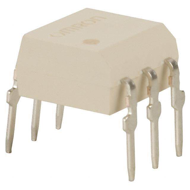
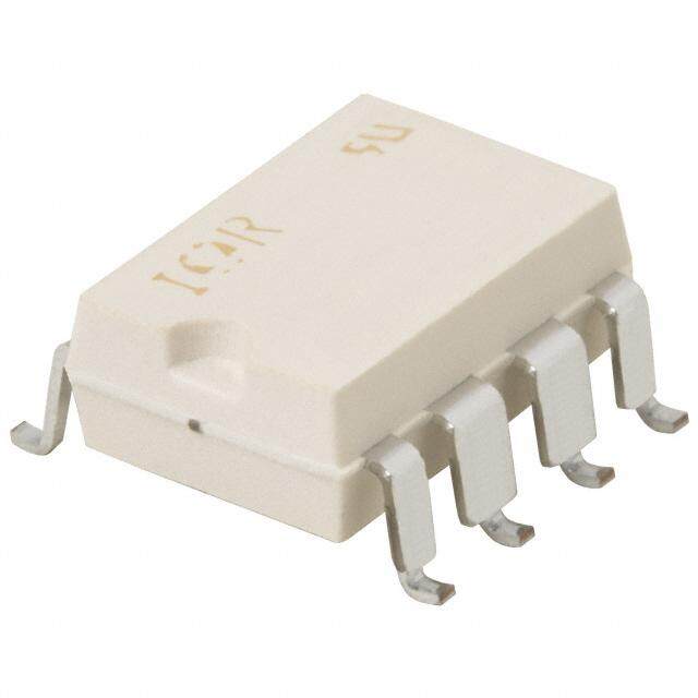
- 型号: G3VM-VF
- 制造商: Omron Electronics LLC
- 库位|库存: xxxx|xxxx
- 要求:
| 数量阶梯 | 香港交货 | 国内含税 |
| +xxxx | $xxxx | ¥xxxx |
查看当月历史价格
查看今年历史价格
G3VM-VF产品简介:
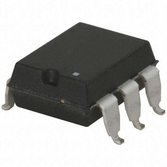
ICGOO电子元器件商城为您提供G3VM-VF由Omron Electronics LLC设计生产,在icgoo商城现货销售,并且可以通过原厂、代理商等渠道进行代购。 G3VM-VF价格参考¥11.84-¥20.26。Omron Electronics LLCG3VM-VF封装/规格:固态继电器, 固体继电器 继电器 SPST-NO(1 Form A) 6-SMD(0.300",7.62mm)。您可以下载G3VM-VF参考资料、Datasheet数据手册功能说明书,资料中有G3VM-VF 详细功能的应用电路图电压和使用方法及教程。
欧姆龙电子有限公司(Omron Electronics Inc-EMC Div)生产的固态继电器G3VM-VF,是一款广泛应用于工业自动化和电气控制系统中的电子开关元件。该型号属于光耦合型固态继电器,具有无触点、寿命长、响应快、抗干扰能力强等特点。

G3VM-VF常用于以下应用场景:

1. 工业自动化控制:如PLC(可编程逻辑控制器)系统中作为输出模块,控制电机、电磁阀、指示灯等负载设备的通断。

2. 温度控制系统:用于加热器或冷却设备的开关控制,实现精准的温度调节。

3. 电力设备控制:适用于小型电气设备的电源控制,如变频器、伺服驱动器等外围电路的切换。

4. 测试与测量设备:在自动测试设备(ATE)中作为信号或电源切换元件,实现高效、稳定的测试流程。

5. 医疗器械:用于需要高可靠性和安全性的医疗设备中,实现对设备各功能模块的电气隔离与控制。

6. 楼宇自动化系统:如照明控制、安防系统、通风设备等,提供稳定可靠的无触点开关解决方案。

G3VM-VF适用于低电压、中小电流负载的场合,具有良好的电气隔离性能,适合对系统稳定性与寿命有较高要求的应用环境。
| 参数 | 数值 |
| 产品目录 | |
| 描述 | RELAY SSR SPST 300MA 6-SMT 60V固态继电器-PCB安装 60V SPST-NO SMD6 SMT 300mA 1.4ohm 170pF |
| 产品分类 | |
| 品牌 | Omron Electronics |
| 产品手册 | |
| 产品图片 |
|
| rohs | 符合RoHS无铅 / 符合限制有害物质指令(RoHS)规范要求 |
| 产品系列 | 固态继电器,固态继电器-PCB安装,Omron Electronics G3VM-VFG3VM |
| mouser_ship_limit | 该产品可能需要其他文件才能进口到中国。 |
| 数据手册 | |
| 产品型号 | G3VM-VF |
| 产品 | Power Relays |
| 产品培训模块 | http://www.digikey.cn/PTM/IndividualPTM.page?site=cn&lang=zhs&ptm=25458http://www.digikey.cn/PTM/IndividualPTM.page?site=cn&lang=zhs&ptm=26145 |
| 产品目录绘图 |
|
| 产品目录页面 | |
| 产品种类 | 固态继电器-PCB安装 |
| 产品类型 | PCB Mount |
| 供应商器件封装 | 6-SMD |
| 其它名称 | G3VM-VF-S |
| 其它有关文件 | |
| 包装 | 管件 |
| 商标 | Omron Electronics |
| 安装类型 | 表面贴装 |
| 安装风格 | SMD/SMT |
| 导通电阻 | 2 欧姆 |
| 封装 | Tube |
| 封装/外壳 | 6-SMD(0.300",7.62mm) |
| 封装/箱体 | SMD DIP-6 |
| 工厂包装数量 | 50 |
| 控制电压范围 | 1 V to 1.3 V |
| 标准包装 | 200 |
| 电压-负载 | 0 ~ 60 V |
| 电压-输入 | 1.15VDC |
| 电路 | SPST-NO(1 A 形) |
| 相关产品 | /product-detail/zh/Y92BA100/Z927-ND/206398/product-detail/zh/Y92B-N100/Z925-ND/206396/product-detail/zh/Y92B-N50/Z924-ND/206395 |
| 端子类型 | 鸥翼型 |
| 端接类型 | Gull Wing Lead |
| 系列 | G3VM |
| 继电器类型 | |
| 触点形式 | SPST (1 Form A) |
| 负载电压额定值 | 60 V |
| 负载电流 | 300mA |
| 负载电流额定值 | 300 mA |
| 输入电流 | 50 mA |
| 输入转输出绝缘方法 | Optocoupler |
| 输出类型 | AC,DC |
| 输出设备 | MOSFET |


- 商务部:美国ITC正式对集成电路等产品启动337调查
- 曝三星4nm工艺存在良率问题 高通将骁龙8 Gen1或转产台积电
- 太阳诱电将投资9.5亿元在常州建新厂生产MLCC 预计2023年完工
- 英特尔发布欧洲新工厂建设计划 深化IDM 2.0 战略
- 台积电先进制程称霸业界 有大客户加持明年业绩稳了
- 达到5530亿美元!SIA预计今年全球半导体销售额将创下新高
- 英特尔拟将自动驾驶子公司Mobileye上市 估值或超500亿美元
- 三星加码芯片和SET,合并消费电子和移动部门,撤换高东真等 CEO
- 三星电子宣布重大人事变动 还合并消费电子和移动部门
- 海关总署:前11个月进口集成电路产品价值2.52万亿元 增长14.8%

PDF Datasheet 数据手册内容提取
MOS FET Relays G3VM Series Wide Range of Contact Forms, Sizes and Package Types •Controls load voltages up to 600 V. (cid:127)Terminal packages include PCB through-hole, SMT gullwing, SOP, and SSOP. (cid:127)Low ON-resistance, low output capacitance, current limiting, and high dielectric (5000 VAC) models available. (cid:127)Packaged for efficient automatic insertion: PCB through- hole and SMT are in tubes; tape-and-reel packaging is standard for SOP and SSOP models, and optional for SMT models (“TR” suffix). (cid:127)Complete specifications follow, divided by Package Type, Terminals and Contact Form. Typical Applications ■ Communications •Local area network equipment (cid:127)Central office circuit boards for subscriber line interfaces, multiplexers and other routing equipment (cid:127)Wireless communications for cell phones and pagers (cid:127)Set-top TV boxes with internal modems (cid:127)Fax machines (cid:127)PCMCIA card (cid:127)Internal modems for PDA equipment and laptop computers ■ Test & Measurement (cid:127)Board testers (cid:127)IC testers (cid:127)Portable voltage testers ■ Security (cid:127)Alarm control boards (cid:127)Home security systems (cid:127)Garage door openers MOS FET Relays G3VM Series 23
Selection Guide Load Contact Package/ No. of Model Load Voltage ON Output Additional Page no. voltage form Terminal terminals current withstand resistance capacitance features shape (mA) (VAC) (max.) 20V 1 Form A SMT 8 G3VM-22FO 150 2,500 4 Ω 8 pF (typ.) Low ON 62 resistance SOP 4 G3VM-21GR 160 1,500 8 Ω 2.5 pF (max.) Low pF(cid:127)Ω 70 G3VM-21GR1 300 1,500 1.5 Ω 12 pF (max.) Low pF(cid:127)Ω 70 SSOP 4 G3VM-21LR 150 1,500 8 Ω 12 pF (max.) — 88 G3VM-21LR1 300 1,500 1.5 Ω 12 pF (max.) Low pF(cid:127)Ω 88 40V 1 Form A SOP 4 G3VM-41GR3 80 1,500 37 Ω 1.4 pF (max.) — 72 G3VM-41GR4 250 1,500 3 Ω 7 pF (max.) Low pF(cid:127)Ω 74 G3VM-41GR5 300 1,500 1.5 Ω 14 pF (max.) Low pF(cid:127)Ω 74 G3VM-41GR6 120 1,500 15 Ω 2 pF (max.) Low pF(cid:127)Ω 74 SSOP 4 G3VM-41LR3 80 1,500 35 Ω 1.4 pF (max.) — 88 G3VM-41LR4 250 1,500 3 Ω 7 pF (max.) Low pF(cid:127)Ω 90 G3VM-41LR5 300 1,500 1.5 Ω 14 pF (max.) Low pF(cid:127)Ω 90 G3VM-41LR6 120 1,500 15 Ω 2 pF (max.) Low pF(cid:127)Ω 90 60V 1 Form A Thru-hole 4 G3VM-61A 500 2,500 2 Ω 140 pF (max.) Low ON 32 resistance G3VM-61A1 500 2,500 2 Ω 130 pF (typ.) Low ON 34 resistance 6 G3VM-61B 500 2,500 2 Ω 140 pF (max.) Low ON 38 resistance G3VM-61B1 500 2,500 2 Ω 130 pF (typ.) Low ON 40 resistance G3VM-V 300 2,500 2 Ω 170 pF (typ.) Low ON 40 resistance 8 G3VM-61CP 500 2,500 0.6 Ω 500 pF (max.) Low ON 42 resistance G3VM-61CR 2000 1,500 0.12 Ω 1400 pF (max.) Low ON 44 resistance SMT 4 G3VM-61D 500 2,500 2 Ω 140 pF (max.) Low ON 52 resistance G3VM-61D1 500 2,500 2 Ω 130 pF (typ.) Low ON 54 resistance 6 G3VM-61E 500 2,500 2 Ω 140 pF (max.) Low ON 58 resistance G3VM-61E1 500 2,500 2 Ω 130 pF (typ.) Low ON 60 resistance 60 V 1 Form A SMT 6 G3VM-VF 300 2,500 2 Ω 170 pF (typ.) Low ON 60 resistance 8 G3VM-61FP 500 2,500 0.6 Ω 500 pF (max.) Low ON 64 resistance G3VM-61FR 2000 1,500 0.12 Ω 1400 pF (max.) Low ON 64 resistance SOP 4 G3VM-61G1 400 1,500 2 Ω 130 pF (typ.) Low ON 76 resistance G3VM-S1 400 1,500 2 Ω 140 pF (max.) Low ON 76 resistance 6 G3VM-61H1 400 1,500 2 Ω 130 pF (typ.) Low ON 80 resistance 2 Form A Thru-hole 8 G3VM-62C1 500 2,500 2 Ω 130 pF (typ.) Low ON 46 resistance SMT 8 G3VM-62F1 500 2,500 2 Ω 130 pF (typ.) Low ON 66 resistance SOP 8 G3VM-62J1 400 1,500 2 Ω 130 pF (typ.) Low ON 84 resistance G3VM-SY 300 1,500 2 Ω 140 pF (max.) Low ON 86 resistance 80 V 1 Form A SOP 4 G3VM-81G1 350 1,500 1.2 Ω 40 pF (max.) Low ON 76 resistance 6 G3VM-81HR 1250 1,500 0.15 Ω 1000 pF (max.) Low ON 80 resistance 200 V 1 Form A SOP 4 G3VM-S5 150 1,500 8 Ω 100 pF (typ.) — 78 24 MOS FET Relays G3VM Series
Load Contact Package/ No. of Model Load Voltage ON Output Additional Page no. voltage form Terminal terminals current withstand resistance capacitance features shape (mA) (VAC) (max.) 350 V 1 Form A Thru-hole 4 G3VM-2 120 2,500 35 Ω 75 pF (typ.) — 30 G3VM-2L 120 2,500 35 Ω 75 pF (typ.) Current 30 limiting G3VM-351A 120 2,500 35 Ω 30 pF (typ.) — 30 6 G3VM-351B 120 2,500 35 Ω 30 pF (typ) — 34 G3VM-3 120 2,500 35 Ω 75 pF (typ) — 36 G3VM-3L 120 2,500 35 Ω 75 pF (typ.) Current 36 limiting 350 V 1 Form A SMT 4 G3VM-2F 120 2,500 35 Ω 75 pF (typ.) — 50 G3VM-2FL 120 2,500 35 Ω 75 pF (typ.) Current 50 limiting G3VM-351D 120 2,500 35 Ω 30 pF (typ.) — 50 6 G3VM-351E 120 2,500 35 Ω 30 pF (typ.) — 54 G3VM-3F 120 2,500 35 Ω 75 pF (typ.) — 56 G3VM-3FL 120 2,500 35 Ω 75 pF (typ.) Current 56 limiting SOP 4 G3VM-351G 110 1,500 35 Ω 30 pF (typ.) — 70 G3VM-S2 120 1,500 35 Ω 75 pF (typ.) — 78 6 G3VM-351H 110 1,500 35 Ω 30 pF (typ.) — 78 G3VM-S3 120 1,500 35 Ω 75 pF (typ.) — 82 1 Form A Thru-hole 8 G3VM-355CR 120 2,500 25 Ω 65 pF (typ.) — 44 + SMT 8 G3VM-355FR 120 2,500 25 Ω 65 pF (typ.) — 64 1 Form B SOP 8 G3VM-355JR 120 2,500 25 Ω 65 pF (typ.) — 82 2 Form A Thru-hole 8 G3VM-352C 120 2,500 35 Ω 30 pF (typ.) — 44 G3VM-W 120 2,500 35 Ω 75 pF (typ.) — 46 G3VM-WL 120 2,500 35 Ω 75 pF (typ.) Current 48 limiting SMT 8 G3VM-352F 120 2,500 35 Ω 30 pF (typ.) — 66 G3VM-WF 120 2,500 35 Ω 75 pF (typ.) — 68 G3VM-WFL 120 2,500 35 Ω 75 pF (typ.) Current 68 limiting SOP 8 G3VM-352J 110 1,500 35 Ω 30 pF (typ.) — 82 G3VM-SW 120 1,500 35 Ω 75 pF (typ.) — 84 1 Form B Thru-hole 4 G3VM-353A 150 2,500 25 Ω 100 pF (typ.) — 32 6 G3VM-353B 150 2,500 25 Ω 100 pF (typ.) — 34 SMT 4 G3VM-353D 150 2,500 25 Ω 100 pF (typ.) — 52 6 G3VM-353E 150 2,500 25 Ω 100 pF (typ.) — 54 350 V 1 Form B SOP 4 G3VM-353G 120 1,500 25 Ω 130 pF (typ.) — 72 6 G3VM-353H 120 1,500 25 Ω 65 pF (typ.) — 80 2 Form B Thru-hole 8 G3VM-354C 120 2,500 35 Ω 100 pF (typ.) — 48 SMT 8 G3VM-354F 120 2,500 35 Ω 100 pF (typ.) — 68 SOP 8 G3VM-354J 120 1,500 25 Ω 65 pF (typ.) — 86 400 V 1 Form A Thru-hole 4 G3VM-401A 120 2,500 35 Ω 70 pF (typ.) — 32 6 G3VM-401B 120 2,500 35 Ω 75 pF (typ.) — 36 G3VM-401BY 120 5,000 35 Ω 75 pF (typ.) High I/O 38 isolation SMT 4 G3VM-401D 120 2,500 35 Ω 70 pF (typ.) — 52 6 G3VM-401E 120 2,500 35 Ω 75 pF (typ.) — 56 G3VM-401EY 120 5,000 35 Ω 75 pF (typ.) High I/O 58 isolation SOP 4 G3VM-401G 120 1,500 35 Ω 70 pF (typ.) — 72 2 Form A Thru-hole 8 G3VM-402C 120 2,500 35 Ω 70 pF (typ.) — 46 SMT 8 G3VM-402F 120 2,500 35 Ω 70 pF (typ.) — 66 SOP 8 G3VM-402J 120 2,500 35 Ω 70 pF (typ.) — 84 600 V 1 Form A Thru-hole 6 G3VM-601BY 100 5,000 45 Ω 100 pF (typ.) High I/O 38 isolation SMT 6 G3VM-601EY 100 5,000 35 Ω 100 pF (typ.) High I/O 58 isolation MOS FET Relays G3VM Series 25
Part Number Index and Ordering Information Note:“G3VM” is not printed on the actual product. Modelname LotNo. The following tables show standard quantities of G3VM relays as shipped in tubes or tape-and-reel packaging. Dimensions for tape-and-reel parts are shown in individual data sheets that follow. Description Packaging Standard pack Model Page quantity no. MOSFET THRU-HOLE RELAY Tube 50 G3VM-2 30 MOSFET SMT RELAY Tube 50 G3VM-2F 50 MOSFET SMT RELAY Tape-and-reel 1500 G3VM-2F(TR) 50 MOSFET SMT RELAY Tube 50 G3VM-2FL 50 MOSFET SMT RELAY Tape-and-reel 1500 G3VM-2FL(TR) 50 MOSFET THRU-HOLE RELAY Tube 50 G3VM-2L 30 MOSFET SOP RELAY Tube 50 G3VM-21GR 70 MOSFET SOP RELAY Tape-and-reel 2500 G3VM-21GR(TR) 70 MOSFET SOP RELAY Tube 50 G3VM-21GR1 70 MOSFET SOP RELAY Tape-and-reel 2500 G3VM-21GR1(TR) 70 MOSFET SSOP RELAY Tape-and-reel 1500 G3VM-21LR 88 MOSFET SSOP RELAY Tape-and-reel 1500 G3VM-21LR1 88 MOSFET SMT RELAY Tube 50 G3VM-22FO 62 MOSFET SMT RELAY Tape-and-reel 1500 G3VM-22FO(TR) 62 MOSFET THRU-HOLE RELAY Tube 50 G3VM-3 36 MOSFET SMT RELAY Tube 50 G3VM-3F 56 MOSFET SMT RELAY Tape-and-reel 1500 G3VM-3F(TR) 56 MOSFET SMT RELAY Tube 50 G3VM-3FL 56 MOSFET SMT RELAY Tape-and-reel 1500 G3VM-3FL(TR) 56 MSOFET THRU-HOLE RELAY Tube 50 G3VM-3L 36 MOSFET THRU-HOLE RELAY Tube 50 G3VM-351A 30 MOSFET THRU-HOLE RELAY Tube 50 G3VM-351B 34 MOSFET SMT RELAY Tube 50 G3VM-351D 50 MOSFET SMT RELAY Tape-and-reel 1500 G3VM-351D(TR) 50 MOSFET SMT RELAY Tube 50 G3VM-351E 54 MOSFET SMT RELAY Tape-and-reel 1500 G3VM-351E(TR) 54 MOSFET SOP RELAY Tube 50 G3VM-351G 70 MOSFET SOP RELAY Tape-and-reel 2500 G3VM-351G(TR) 70 MOSFET SOP RELAY Tube 50 G3VM-351H 78 MOSFETSOP RELAY Tape-and-reel 2500 G3VM-351H(TR) 78 MOSFET THRU-HOLE RELAY Tube 50 G3VM-352C 44 MOSFET SMT RELAY Tube 50 G3VM-352F 66 MOSFET SMT RELAY Tape-and-reel 1500 G3VM-352F(TR) 66 MOSFET SOP RELAY Tube 50 G3VM-352J 82 MOSFET SOP RELAY Tape-and-reel 2500 G3VM-352J(TR) 82 26 MOS FET Relays G3VM Series
Description Packaging Standard pack Model Page quantity no. MOSFET THRU-HOLE RELAY Tube 50 G3VM-353A 32 MOSFET THRU-HOLE RELAY Tube 50 G3VM-353B 34 MOSFET SMT RELAY Tube 50 G3VM-353D 52 MOSFET SMT RELAY Tape-and-reel 1500 G3VM-353D(TR) 52 MOSFET SMT RELAY Tube 50 G3VM-353E 54 MOSFET SMT RELAY Tape-and-reel 1500 G3VM-353E(TR) 54 MOSFET SOP RELAY Tube 50 G3VM-353G 72 MOSFET SOP RELAY Tape-and-reel 2500 G3VM-353G(TR) 72 MOSFET SOP RELAY Tube 50 G3VM-353H 80 MOSFET SOP RELAY Tape-and-reel 2500 G3VM-353H(TR) 80 MOSFET THRU-HOLE RELAY Tube 50 G3VM-354C 48 MOSFET SMT RELAY Tube 50 G3VM-354F 68 MOSFET SMT RELAY Tape-and reel 1500 G3VM-354F(TR) 68 MOSFET SOP RELAY Tube 50 G3VM-354J 86 MOSFET SOP RELAY Tape-and-reel 2500 G3VM-354J(TR) 86 MOSFET THRU-HOLE RELAY Tube 50 G3VM-355CR 44 MOSFET SMT RELAY Tube 50 G3VM-355FR 64 MOSFET SMT RELAY Tape-and-reel 1500 G3VM-355FR(TR) 64 MOSFET SOP RELAY Tube 50 G3VM-355JR 82 MOSFET SOP RELAY Tape-and-reel 2500 G3VM-355JR(TR) 82 MOSFET SOP RELAY Tube 50 G3VM-41GR3 72 MOSFET SOP RELAY Tape-and-reel 2500 G3VM-41GR3(TR) 72 MOSFET SOP RELAY Tube 50 G3VM-41GR4 74 MOSFET SOP RELAY Tape-and-reel 2500 G3VM-41GR4(TR) 74 MOSFET SOP RELAY Tube 50 G3VM-41GR5 74 MOSFET SOP RELAY Tape-and-reel 2500 G3VM-41GR5(TR) 74 MOSFET SOP RELAY Tube 50 G3VM-41GR6 74 MOSFET SOP RELAY Tape-and reel 2500 G3VM-41GR6(TR) 74 MOSFET SSOP RELAY Tape-and-reel 1500 G3VM-41LR3 88 MOSFET SSOP RELAY Tape-and-reel 1500 G3VM-41LR4 90 MOSFET SSOP RELAY Tape-and-reel 1500 G3VM-41LR5 90 MOSFET SSOP RELAY Tape-and-reel 1500 G3VM-41LR6 90 MOSFET THRU-HOLE RELAY Tube 50 G3VM-401A 32 MOSFET THRU-HOLE RELAY Tube 50 G3VM-401B 36 MOSFET THRU-HOLE RELAY Tube 50 G3VM-401BY 38 MOSFET SMT RELAY Tube 50 G3VM-401D 52 MOSFET SMT RELAY Tape-and-reel 1500 G3VM-401D(TR) 52 MOSFET SMT RELAY Tube 50 G3VM-401E 56 MOSFET SMT RELAY Tape-and-reel 1500 G3VM-401E(TR) 56 MOSFET SMT RELAY Tube 50 G3VM-401EY 58 MOSFET SMT RELAY Tape-and-reel 1500 G3VM-401EY(TR) 58 This table continues on the next page. MOS FET Relays G3VM Series 27
Description Packaging Standard pack Model Page quantity no. MOSFET SOP RELAY Tube 50 G3VM-401G 72 MOSFET SOP RELAY Tape-and-reel 2500 G3VM-401G(TR) 72 MOSFET THRU-HOLE RELAY Tube 50 G3VM-402C 46 MOSFET SMT RELAY Tube 50 G3VM-402F 66 MOSFET SMT RELAY Tape-and-reel 1500 G3VM-402F(TR) 66 MOSFET SOP RELAY Tube 50 G3VM-402J 84 MOSFET SOP RELAY Tape-and reel 2500 G3VM-402J(TR) 84 MOSFET THRU-HOLE RELAY Tube 50 G3VM-61A 32 MOSFET THRU-HOLE RELAY Tube 50 G3VM-61A1 34 MOSFET THRU-HOLE RELAY Tube 50 G3VM-61B 38 MOSFET THRU-HOLE RELAY Tube 50 G3VM-61B1 40 MOSFET THRU-HOLE RELAY Tube 50 G3VM-61CP 42 MOSFET THRU-HOLE RELAY Tube 50 G3VM-61CR 44 MOSFET SMT RELAY Tube 50 G3VM-61D 52 MOSFET SMT RELAY Tape-and-reel 1500 G3VM-61D(TR) 52 MOSFET SMT RELAY Tube 50 G3VM-61D1 54 MOSFET SMT RELAY Tape-and-reel 1500 G3VM-61D1(TR) 54 MOSFET SMT RELAY Tube 50 G3VM-61E 58 MOSFET SMT RELAY Tape-and-reel 1500 G3VM-61E(TR) 58 MOSFET SMT RELAY Tube 50 G3VM-61E1 60 MOSFET SMT RELAY Tape-and-reel 1500 G3VM-61E1(TR) 60 MOSFET SMT RELAY Tube 50 G3VM-61FP 64 MOSFET SMT RELAY Tape-and-reel 1500 G3VM-61FP(TR) 64 MOSFET SMT RELAY Tube 50 G3VM-61FR 64 MOSFET SMT RELAY Tape-and-reel 1500 G3VM-61FR(TR) 64 MOSFET SOP RELAY Tube 50 G3VM-61G1 76 MOSFET SOP RELAY Tape-and-reel 2500 G3VM-61G1(TR) 76 MOSFET SOP RELAY Tube 50 G3VM-61H1 80 MOSFET SOP RELAY Tape-and-reel 2500 G3VM-61H1(TR) 80 MOSFET THRU-HOLE RELAY Tube 50 G3VM-62C1 46 MOSFET SMT RELAY Tube 50 G3VM-62F1 66 MOSFET SMT RELAY Tape-and-reel 1500 G3VM-62F1(TR) 66 MOSFET SOP RELAY Tube 50 G3VM-62J1 84 MOSFET SOP RELAY Tape-and-reel 2500 G3VM-62J1(TR) 84 MOSFET THRU-HOLE RELAY Tube 50 G3VM-601BY 38 MOSFET SMT RELAY Tube 50 G3VM-601EY 58 MOSFET SMT RELAY Tape-and-reel 1500 G3VM-601EY(TR) 58 MOSFET SOP RELAY Tube 50 G3VM-81G1 76 MOSFET SOP RELAY Tape-and-reel 2500 G3VM-81G1(TR) 76 MOSFET SOP RELAY Tube 50 G3VM-81HR 80 MOSFET SOP RELAY Tape-and-reel 2500 G3VM-81HR(TR) 80 28 MOS FET Relays G3VM Series
Description Packaging Standard pack Model Page quantity no. MOSFET SOP RELAY Tube 50 G3VM-S1 76 MOSFET SOP RELAY Tape-and-reel 2500 G3VM-S1(TR) 76 MOSFET SOP RELAY Tube 50 G3VM-S2 78 MOSFET SOP RELAY Tape-and-reel 2500 G3VM-S2(TR) 78 MOSFET SOP RELAY Tube 50 G3VM-S3 82 MOSFET SOP RELAY Tape-and-reel 2500 G3VM-S3(TR) 82 MOSFET SOP RELAY Tube 50 G3VM-S5 78 MOSFET SOP RELAY Tape-and-reel 2500 G3VM-S5(TR) 78 MOSFET SOP RELAY Tube 50 G3VM-SW 84 MOSFET SOP RELAY Tape-and-reel 2500 G3VM-SW(TR) 84 MOSFET SOP RELAY Tube 50 G3VM-SY 86 MOSFET SOP RELAY Tape-and-reel 2500 G3VM-SY(TR) 86 MOSFET THRU-HOLE RELAY Tube 50 G3VM-V 40 MOSFET SMT RELAY Tube 50 G3VM-VF 60 MOSFET SMT RELAY Tape-and-reel 1500 G3VM-VF(TR) 60 MOSFET THRU-HOLE RELAY Tube 50 G3VM-W 46 MOSFET SMT RELAY Tube 50 G3VM-WF 68 MOSFET SMT RELAY Tape-and-reel 1500 G3VM-WF(TR) 68 MOSFET SMT RELAY Tube 50 G3VM-WFL 68 MOSFET SMT RELAY Tape-and-reel 1500 G3VM-WFL(TR) 68 MOSFET THRU-HOLE RELAY Tube 50 G3VM-WL 48 Specifications tables begin on the following page. MOS FET Relays G3VM Series 29
Specifications G3VM-2, -2L, -351A Maximum Rating Parameter Comments and conditions G3VM-2 G3VM-2L G3VM-351A Contact form/no. of terminals — 1 Form A/4 pins 1 Form A/4 pins 1 Form A/4 pins Input (LED) LED forward current I Typical 50 mA 50 mA 50 mA F I (100 µs pulse, Max. 1 A 1 A 1 A FP 100 pps) Forward current Ta ≥ 25°C -0.5 mA/°C -0.5 mA/°C -0.5 mA/°C derating Reverse voltage V Max. 5 V 6 V 5 V R Junction temperature (T) 125°C 125°C 125°C J Output (Detector) Output voltage V 350 V 350 V 350 V OFF strength (AC or DC peak) Continuous load I 120 mA 120 mA 120 mA O current ON-state current Ta ≥ 25°C -1.2 mA/°C -1.2 mA/°C -1.2 mA/°C derating Junction temperature (T) 125°C 125°C 125°C J Dielectric strength V for 1 minute min. 2500 VAC 2500 VAC 2500 VAC I/O Temperature Ambient Ta with no icing -20° to +85°C -40° to +85°C -40° to +85°C Storage Tstg with no icing -55° to +100°C -55° to +125°C -55° to +125°C Electrical Characteristics Parameter Comments and conditions G3VM-2 G3VM-2L G3VM-351A Input LED forward voltage I =10 mA Min. 1.0 V 1.0 V 1.0 V F (VF) Typical 1.15 V 1.15 V 1.15 V Max. 1.3 V 1.3 V 1.3 V Reverse current I Max. 10 µA 10 µA 10 µA R Reverse voltage V Max. 5 V 6 V 5 V R Capacitance (C ) V = 0; Typical 30 pF 30 pF 30 pF T freq. = 1 MHz Keep ON LED current I = 120 mA Typical 2 mA 1 mA 1 mA O (IFT) Max. 3 mA 3 mA 3 mA Output ON-resistance (R ) I =120 mA Typical 22 Ω 22 Ω 35 Ω (25 Ω, t< 1s) ON ON I =5 mA Max. 35 Ω 35 Ω 50 Ω (35 Ω, t< 1s) F OFF-state leakage V = 350 V Max. 1.0 µA 1.0 µA 1.0 µA OFF current (I ) LEAK Limit current (I ) I = 5 mA, V = 5 V, Min. — 150 mA — LIM F DD t = 5 ms Max. — 300 mA — Transfer I/O capacitance (C ) Typical 0.8 pF 0.8 pF 0.8 pF I/O characteristics I/O resistance (R ) Min. 1000 MΩ 1000 MΩ 1000 MΩ IO Operate time (t ) Max. 1.0 ms 1.0 ms 1.0 ms ON Release time (t ) Max. 1.0 ms 1.0 ms 1.0 ms OFF 30 MOS FET Relays G3VM Series
Optimum Operating Conditions Parameter Comments and conditions G3VM-2 G3VM-2L G3VM-351A Output voltage strength V Max. 280 V 280 V 280 V DD Operate LED forward current I Min. 5 mA 5 mA 5 mA F Typical 7.5 mA 7.5 mA 7.5 mA Max. 25 mA 25 mA 25 mA Continuous load current I Max. 100 mA 100 mA 100 mA O Ambient temperature T -20° to 65°C -20° to 65°C -20° to 65°C A Dimensions Item G3VM-2 G3VM-2L G3VM-351A Dimensions See page 92 See page 92 See page 92 Connections G3VM-2, 2L G3VM-2, 2L, 351A Timing Chart MOS FET Relays G3VM Series 31
G3VM-353A, -401A, -61A Maximum Rating Parameter Comments and conditions G3VM-353A G3VM-401A G3VM-61A Contact form/no. of terminals — 1 Form B/4 pins 1 Form A/4 pins 1 Form A/4 pins Input (LED) LED forward current I Typical 50 mA 50 mA 50 mA F I (100 µs pulse, Max. 1 A 1 A 1 A FP 100 pps) Forward current Ta ≥ 25°C -0.5 mA/°C -0.5 mA/°C -0.5 mA/°C derating Reverse voltage V Max. 5 V 5 V 5 V R Junction temperature (T) 125°C 125°C 125°C J Output (Detector) Output voltage V 350 V 400 V 60 V OFF strength Continuous load I 150 mA 120 mA 500 mA O current ON-state current Ta ≥ 25°C -1.5 mA/°C -1.2 mA/°C -5.0 mA/°C derating Junction temperature (T) 125°C 125°C 125°C J Dielectric strength V for 1 minute min. 2500 VAC 2500 VAC 2500 VAC I/O Temperature Ambient Ta with no icing -40° to +85°C -40° to +85°C -40° to +85°C Storage Tstg with no icing -55° to +125°C -55° to +125°C -55° to +125°C Electrical Characteristics Parameter Comments and conditions G3VM-353A G3VM-401A G3VM-61A Input LED forward voltage I =10 mA Min. 1.0 V 1.0 V 1.0 V F (VF) Typical 1.15 V 1.15 V 1.15 V Max. 1.3 V 1.3 V 1.3 V Reverse current I Max. 10 µA 10 µA 10 µA R Reverse voltage V Max. 5 V 5 V 5 V R Capacitance (C ) V = 0; Typical 30 pF 30 pF 30 pF T freq. = 1 MHz Keep ON LED current I = 120 mA Typical 1 mA 1 mA 1 mA O (IFT) Max. 3 mA 3 mA 3 mA Output ON-resistance (R ) I =150 mA Typical 15 Ω 18 Ω 1 Ω (I =500 mA) ON ON ON IF=5 mA Max. 25 Ω 35 Ω 2 Ω (ION=500 mA) OFF-state leakage At V Max. 1.0 µA 1.0 µA 1.0 µA OFF current (I ) LEAK Limit current (I ) I = 5 mA, V = 5 V, Min. — — — LIM F DD t = 5 ms Max. — — — Transfer I/O capacitance (C ) Typical 0.8 pF 0.8 pF 0.8 pF I/O characteristics I/O resistance (R ) Min. 1000 MΩ 1000 MΩ 1000 MΩ IO Operate time (t ) Max. 1.0 ms 1.0 ms 1.0 ms ON (I = 10 mA) F Release time (t ) Max. 3.0 ms 1.0 ms 1.0 ms OFF (I = 10 mA) F Optimum Operating Conditions Parameter Comments and conditions G3VM-353A G3VM-401A G3VM-61A Output voltage strength V Max. 280 V 320 V 48 V DD Operate LED forward current I Min. 5 mA 5 mA 5 mA F Typical — 7.5 mA 7.5 mA Max. 25 mA 25 mA 25 mA Continuous load current I Max. 150 mA 100 mA 400 mA O Ambient temperature T -20° to 65°C -20° to 65°C -20° to 65°C A 32 MOS FET Relays G3VM Series
Dimensions Item G3VM-353A G3VM-401A G3VM-61A Dimensions See page 92 See page 92 See page 92 Connections G3VM-353A, 401A, 61A G3VM-353A Timing Chart MOS FET Relays G3VM Series 33
G3VM-61A1, -351B, -353B Maximum Rating Parameter Comments and conditions G3VM-61A1 G3VM-351B G3VM-353B Contact form/no. of terminals — 1 Form A/4 pins 1 Form A/6 pins 1 Form B/6 pins Input (LED) LED forward current I Typical 50 mA 50 mA 50 mA F I (100 µs pulse, Max. 1 A 1 A 1 A FP 100 pps) Forward current Ta ≥ 25°C -0.5 mA/°C -0.5 mA/°C -0.5 mA/°C derating Reverse voltage V Max. 5 V 5 V 5 V R Junction temperature (T) 125°C 125°C 125°C J Output (Detector) Output voltage V 60 V 350 V 350 V OFF strength Continuous load I 500 mA 120 mA (for A) 150 mA (for A) O current 120 mA (for B) 150 mA (for B) 240 mA (for C) 300 mA (for C) ON-state current Ta ≥ 25°C -5.0 mA/°C -1.2 mA/°C (for A) -1.5 mA/°C (for A) derating Junction temperature (T) 125°C 125°C 125°C J Dielectric strength V for 1 minute min. 2500 VAC 2500 VAC 2500 VAC I/O Temperature Ambient Ta with no icing -40° to +85°C -40° to +85°C -40° to +85°C Storage Tstg with no icing -55° to +125°C -55° to +125°C -55° to +125°C Electrical Characteristics Parameter Comments and conditions G3VM-61A1 G3VM-351B G3VM-353B Input LED forward voltage I =10 mA Min. 1.0 V 1.0 V 1.0 V F (VF) Typical 1.15 V 1.15 V 1.15 V Max. 1.3 V 1.3 V 1.3 V Reverse current I Max. 10 µA 10 µA 10 µA R Reverse voltage V Max. 5 V 5 V 5 V R Capacitance (C ) V = 0; Typical 30 pF 30 pF 30 pF T freq. = 1 MHz Keep ON LED current I = 120 mA Typical 1.6 mA 1 mA 1 mA O (IFT) Max. 3 mA 3 mA 3 mA Output ON-resistance (R ) I =5 mA Typical 1 Ω (I =500 mA) 35 Ω (I =120 mA) for 15 Ω (I =150 mA) for ON F ON ON ON connection A connection A Max. 2 Ω (I =500 mA) 50 Ω (I =120 mA) for 25 Ω (I =150 mA) for ON ON ON connection A connection A Typical — 28 Ω (I =120 mA) for 8 Ω (I =150 mA) for ON ON connection B connection B Max. — 40 Ω (I =120 mA) for 14 Ω (I =150 mA) for ON ON connection B connection B Typical — 14 Ω (I =240 mA) for 4 Ω (I =300 mA) for ON ON connection C connection C Max. — 20 Ω (I =240 mA) for 7 Ω (I =300 mA) for ON ON connection C connection C OFF-state leakage At V Max. 1.0 µA 1.0 µA 1.0 µA OFF current (I ) LEAK Limit current (I ) I = 5 mA, V = 5 V, Min. — — — LIM F DD t = 5 ms Max. — — — Transfer I/O capacitance (C ) Typical 0.8 pF 0.8 pF 0.8 pF I/O characteristics I/O resistance (R ) Min. 1000 MΩ 1000 MΩ 1000 MΩ IO Operate time (t ) Max. 2.0 ms 1.0 ms 1.0 ms ON Release time (t ) Max. 0.5 ms 1.0 ms 3.0 ms OFF 34 MOS FET Relays G3VM Series
Optimum Operating Conditions Parameter Comments and conditions G3VM-61A1 G3VM-351B G3VM-353B Output voltage strength V Max. 48 V 280 V 280 V DD Operate LED forward current I Min. 5 mA 5 mA 5 mA F Typical 7.5 mA 10 mA — Max. 25 mA 25 mA 25 mA Continuous load current I Max. 500 mA 100 mA 150 mA O Ambient temperature T -20° to 65°C -20° to 65°C -20° to 65°C A Dimensions Item G3VM-61A1 G3VM-351B G3VM-353B Dimensions See page 92 See page 92 See page 92 Connections G3VM-61A1 G3VM-351B, -353B G3VM-351B, -353B Timing Chart MOS FET Relays G3VM Series 35
G3VM-3, -3L, -401B Maximum Rating Parameter Comments and conditions G3VM-3 G3VM-3L G3VM-401B Contact form/no. of terminals — 1 Form A/6 pins 1 Form A/6 pins 1 Form A/6 pins Input (LED) LED forward current I Typical 50 mA 50 mA 50 mA F I (100 µs pulse, Max. 1 A 1 A 1 A FP 100 pps) Forward current Ta ≥ 25°C -0.5 mA/°C -0.5 mA/°C -0.5 mA/°C derating Reverse voltage V Max. 5 V 5 V 5 V R Junction temperature (T) 125°C 125°C 125°C J Output (Detector) Output voltage V 60 V 350 V 400 V OFF strength Continuous load I 120 mA (for A) 120 mA 120 mA (for A) O current 120 mA (for B) 120 mA (for B) 160 mA (for C) 240 mA (for C) ON-state current Ta ≥ 25°C -1.2 mA/°C (for A) -1.2 mA/°C -1.2 mA/°C (for A) derating Junction temperature (T) 125°C 125°C 125°C J Dielectric strength V for 1 minute min. 2500 VAC 2500 VAC 2500 VAC I/O Temperature Ambient Ta with no icing -20° to +85°C -40° to +85°C -40° to +85°C Storage Tstg with no icing -55° to +100°C -55° to +125°C -55° to +125°C Electrical Characteristics Parameter Comments and conditions G3VM-3 G3VM-3L G3VM-401B Input LED forward voltage I =10 mA Min. 1.0 V 1.0 V 1.0 V F (VF) Typical 1.15 V 1.15 V 1.15 V Max. 1.3 V 1.3 V 1.3 V Reverse current I Max. 10 µA 10 µA 10 µA R Reverse voltage V Max. 5 V 5 V 5 V R Capacitance (C ) V = 0; Typical 30 pF 30 pF 30 pF T freq. = 1 MHz Keep ON LED current At I Typical — — 1 mA O (IFT) Max. 3 mA 3 mA 3 mA Output ON-resistance (R ) I =5 mA Typical 22 Ω (I =120 mA) 22 Ω (I =120 mA) 17 Ω (I =120 mA) for ON F ON ON ON for connection A connection A Max. 35 Ω (I =120 mA) 35 Ω (I =120 mA) 35 Ω (I =120 mA) for ON ON ON for connection A connection A Typical 16 Ω (I =120 mA) — 11 Ω (I =120 mA) for ON ON for connection B connection B Max. 23 Ω (I =120 mA) — 20 Ω (I =120 mA) for ON ON for connection B connection B Typical 8 Ω (I =160 mA) — 6 Ω (I =240 mA) for ON ON for connection C connection C Max. 12 Ω (I =160 mA) — 10 Ω (I =240 mA) for ON ON for connection C connection C OFF-state leakage At V Max. 1.0 µA 1.0 µA 1.0 µA OFF current (I ) LEAK Limit current (I ) I = 5 mA, V = 5 V, Min. — 150 mA — LIM F DD t = 5 ms Max. — 300 mA — Transfer I/O capacitance (C ) Typical 0.8 pF 0.8 pF 0.8 pF I/O characteristics I/O resistance (R ) Min. 1000 MΩ 1000 MΩ 1000 MΩ IO Operate time (t ) Max. 1.0 ms 1.0 ms 1.0 ms ON Release time (t ) Max. 1.0 ms 1.0 ms 1.0 ms OFF 36 MOS FET Relays G3VM Series
Optimum Operating Conditions Parameter Comments and conditions G3VM-3 G3VM-3L G3VM-401B Output voltage strength V Max. 280 V 280 V 320 V DD Operate LED forward current I Min. 5 mA 5 mA 5 mA F Typical 7.5 mA 10 mA 7.5 mA Max. 25 mA 25 mA 25 mA Continuous load current I Max. 120 mA 120 mA 120 mA O Ambient temperature T -20° to 65°C -20° to 65°C -20° to 65°C A Dimensions Item G3VM-3 G3VM-3L G3VM-401B Dimensions See page 92 See page 92 See page 92 Connections G3VM-3L G3VM-3, -3L, -401B G3VM-3, -401B Timing Chart MOS FET Relays G3VM Series 37
G3VM-401BY, -601BY, -61B Maximum Rating Parameter Comments and conditions G3VM-401BY G3VM-601BY G3VM-61B Contact form/no. of terminals — 1 Form A/6 pins 1 Form A/6 pins 1 Form A/6 pins Input (LED) LED forward current I Typical 50 mA 50 mA 50 mA F I (100 µs pulse, Max. 1 A 1 A 1 A FP 100 pps) Forward current Ta ≥ 25°C -0.5 mA/°C -0.5 mA/°C -0.5 mA/°C derating Reverse voltage V Max. 5 V 5 V 5 V R Junction temperature (T) 125°C 125°C 125°C J Output (Detector) Output voltage V 400 V 600 V 60 V OFF strength Continuous load I 120 mA (for A) 100 mA (for A) 500 mA (for A) O current 120 mA (for B) 100 mA (for B) 500 mA (for B) 240 mA (for C) 200 mA (for C) 1000 mA (for C) ON-state current Ta ≥ 25°C -1.2 mA/°C (for A) -1.0 mA/°C (for A) -5.0 mA/°C (for A) derating Junction temperature (T) 125°C 125°C 125°C J Dielectric strength V for 1 minute min. 5000 VAC 5000 VAC 2500 VAC I/O Temperature Ambient Ta with no icing -40° to +85°C -40° to +85°C -40° to +85°C Storage Tstg with no icing -55° to +125°C -55° to +125°C -55° to +125°C Electrical Characteristics Parameter Comments and conditions G3VM-401BY G3VM-601BY G3VM-61B Input LED forward voltage I =10 mA Min. 1.0 V 1.0 V 1.0 V F (VF) Typical 1.15 V 1.15 V 1.15 V Max. 1.3 V 1.3 V 1.3 V Reverse current I Max. 10 µA 10 µA 10 µA R Reverse voltage V Max. 5 V 5 V 5 V R Capacitance (C ) V = 0; Typical 30 pF 30 pF 30 pF T freq. = 1 MHz Keep ON LED current At I Typical — — O (IFT) Max. 3 mA 5 mA 3 mA Output ON-resistance (R ) I =5 mA Typical 17 Ω (I =120 mA) 30 Ω (I =100 mA) for 1 Ω (I =500 mA) for ON F ON ON ON for connection A connection A connection A Max. 35 Ω (I =120 mA) 45 Ω (I =100 mA) for 2 Ω (I =500 mA) for ON ON ON for connection A connection A connection A Typical 11 Ω (I =120 mA) 23 Ω (I =100 mA) for 0.5 Ω (I =500 mA) for ON ON ON for connection B connection B connection B Max. 20 Ω (I =120 mA) 35 Ω (I =100 mA) for 1 Ω (I =500 mA) for ON ON ON for connection B connection B connection B Typical 6 Ω (I =240 mA) 12 Ω (I =200 mA) for 0.3 Ω (I =1000 mA) ON ON ON for connection C connection C for connection C Max. 10 Ω (I =240 mA) 18 Ω (I =200 mA) for — ON ON for connection C connection C OFF-state leakage At V Max. 1.0 µA 1.0 µA 1.0 µA OFF current (I ) LEAK Limit current (I ) I = 5 mA, V = 5 V, Min. — — — LIM F DD t = 5 ms Max. — — — Transfer I/O capacitance (C ) Typical 0.8 pF 0.8 pF 0.8 pF I/O characteristics I/O resistance (R ) Min. 1000 MΩ 1000 MΩ 1000 MΩ IO Operate time (t ) Max. 1.0 ms 1.5 ms 1.0 ms ON Release time (t ) Max. 1.0 ms 1.0 ms 1.0 ms OFF 38 MOS FET Relays G3VM Series
Optimum Operating Conditions Parameter Comments and conditions G3VM-401BY G3VM-601BY G3VM-61B Output voltage strength V Max. 320 V 480 V 48 V DD Operate LED forward current I Min. 5 mA 7.5 mA 5 mA F Typical 7.5 mA 15 mA 7.5 mA Max. 25 mA 25 mA 25 mA Continuous load current I Max. 120 mA 100 mA 400 mA O Ambient temperature T -20° to 65°C -20° to 65°C -20° to 65°C A Dimensions Item G3VM-401BY G3VM-601BY G3VM-61B Dimensions See page 92 See page 92 See page 92 Connections G3VM-401BY, -601BY, -61B G3VM-401BY, -601BY, -61B Timing Chart MOS FET Relays G3VM Series 39
G3VM-61B1, -V Maximum Rating Parameter Comments and conditions G3VM-61B1 G3VM-V Contact form/no. of terminals — 1 Form A/6 pins 1 Form A/6 pins Input (LED) LED forward current I Typical 50 mA 50 mA F I (100 µs pulse, 100 Max. 1 A 1 A FP pps) Forward current derating Ta ≥ 25°C -0.5 mA/°C -0.5 mA/°C Reverse voltage V Max. 5 V 5 V R Junction temperature (T) 125°C 125°C J Output (Detector) Output voltage strength V 60 V 60 V OFF Continuous load current I 500 mA (for A) 300 mA (for A) O 500 mA (for B) 450 mA (for B) 1000 mA (for C) 600 mA (for C) ON-state current derating Ta ≥ 25°C -5.0 mA/°C (for A) -3.0 mA/°C (for A) Junction temperature (T) 125°C 125°C J Dielectric strength V for 1 minute min. 2500 VAC 2500 VAC I/O Temperature Ambient Ta with no icing -40° to +85°C -20° to +85°C Storage Tstg with no icing -55° to +125°C -55° to +100°C Electrical Characteristics Parameter Comments and conditions G3VM-61B1 G3VM-V Input LED forward voltage (V ) I =10 mA Min. 1.0 V 1.0 V F F Typical 1.15 V 1.15 V Max. 1.3 V 1.3 V Reverse current I Max. 10 µA 10 µA R Reverse voltage V Max. 5 V 5 V R Capacitance (C ) V = 0; Typical 30 pF 30 pF T freq. = 1 MHz Keep ON LED current (I ) At I Typical 1.6 mA 1 mA FT O Max. 3 mA 5 mA Output ON-resistance (R ) I =5 mA Typical 1 Ω (I =500 mA) for 1.4 Ω (I =300 mA) for ON F ON ON connection A connection A Max. 2 Ω (I =500 mA) for 2 Ω (I =300 mA) for ON ON connection A connection A Typical 0.5 Ω (I =500 mA) for 0.7 Ω (I =450 mA) for ON ON connection B connection B Max. 1 Ω (I =500 mA) for 1 Ω (I =450 mA) for ON ON connection B connection B Typical 0.25 Ω (I =1000 mA) for 0.35 Ω (I =600 mA) for ON ON connection C connection C Max. — 0.5 Ω (I =600 mA) for ON connection C OFF-state leakage current At V Max. 1.0 µA 1.0 µA OFF (I ) LEAK Limit current (I ) I = 5 mA, V = 5 V, Min. — — LIM F DD t = 5 ms Max. — — Transfer I/O capacitance (C ) Typical 0.8 pF 0.8 pF I/O characteristics I/O resistance (R ) Min. 1000 MΩ 1000 MΩ IO Operate time (t ) Max. 2.0 ms 1.0 ms ON Release time (t ) Max. 0.5 ms 1.0 ms OFF 40 MOS FET Relays G3VM Series
Optimum Operating Conditions Parameter Comments and conditions G3VM-61B1 G3VM-V Output voltage strength V Max. 48 V 48V DD Operate LED forward current I Min. 5 mA 7.5 mA F Typical 7.5 mA 15 mA Max. 25 mA 25 mA Continuous load current I Max. 500 mA 300 mA O Ambient temperature T -20° to 65°C -20° to 80°C A Dimensions Item G3VM-61B1 G3VM-V Dimensions See page 92 See page 92 Connections G3VM-61B1, -V G3VM-61B1, -V Timing Chart MOS FET Relays G3VM Series 41
G3VM-61CP Maximum Rating Parameter Comments and conditions G3VM-61CP Contact form/no. of terminals — 1 Form A/8 pins Input (LED) LED forward current I Typical 50 mA F I (100 µs pulse, 100 pps) Max. 1 A FP Forward current derating Ta ≥ 25°C -0.5 mA/°C Reverse voltage V Max. 6 V R Junction temperature (T) 125°C J Output (Detector) Output voltage strength V 60 V OFF Continuous load current I 500 mA O ON-state current derating Ta ≥ 25°C -5.0 mA/°C Junction temperature (T) 125°C J Dielectric strength V for 1 minute min. 2500 VAC I/O Temperature Ambient Ta with no icing -40° to +85°C Storage Tstg with no icing -55° to +125°C Electrical Characteristics Parameter Comments and conditions G3VM-61CP Input LED forward voltage (V ) I =10 mA Min. 1.0 V F F Typical 1.2 V Max. 1.4 V Reverse current I Max. 15 µA R Reverse voltage V Max. 6 V R Capacitance (C ) V = 0; Typical 15 pF T freq. = 1 MHz Keep ON LED current (I ) At I Typical — FT O Max. 5 mA Output ON-resistance (R ) I =5 mA Typical 0.3 Ω (I =500 mA) ON F ON Max. 0.6 Ω (I =500 mA) ON Typical — Max. — Typical — Max. — OFF-state leakage current (I ) At V Max. 1.0 µA LEAK OFF Capacitance COFF Typical 200 pF Max. 500 pF Transfer characteristics I/O capacitance (C ) Typical 0.8 pF I/O I/O resistance (R ) Min. 1000 MΩ IO Operate time (t ) Max. 2.0 ms ON Release time (t ) Max. 0.5 ms OFF 42 MOS FET Relays G3VM Series
Optimum Operating Conditions Parameter Comments and conditions G3VM-61CP Output voltage strength V Max. 48 V DD Operate LED forward current I Min. 10 mA F Typical — mA Max. 30 mA Continuous load current I Max. 500 mA O Ambient temperature T -25° to 50°C A Dimensions Item G3VM-61CP Dimensions See page 93 Connections G3VM-61CP Timing Chart MOS FET Relays G3VM Series 43
G3VM-61CR, 355CR, 352C Maximum Rating Parameter Comments and conditions G3VM-61CR G3VM-355CR G3VM-352C Contact form/no. of terminals — 1 Form A/8 pins 1FormA+1FormB/ 2 Form A/8 pins 8 pins Input (LED) LED forward current I Typical 50 mA 50 mA 50 mA F I (100 µs pulse, Max. 1 A 1 A 1 A FP 100 pps) Forward current Ta ≥ 25°C -0.5 mA/°C -0.5 mA/°C -0.5 mA/°C derating Reverse voltage V Max. 6 V 5 V 5 V R Junction temperature (T) 125°C 125°C 125°C J Output (Detector) Output voltage V 60 V 350 V 350 V OFF strength Continuous load I 2000 mA 120 mA 120 mA O current ON-state current Ta ≥ 25°C -20 mA/°C -1.2 mA/°C -1.2 mA/°C derating Junction temperature (T) 125°C 125°C 125°C J Dielectric strength V for 1 minute min. 1500 VAC 2500 VAC 2500 VAC I/O Temperature Ambient Ta with no icing -20° to +85°C -40° to +85°C -40° to +85°C Storage Tstg with no icing -55° to +125°C -55° to +125°C -55° to +100°C Electrical Characteristics Parameter Comments and conditions G3VM-61CR G3VM-355CR G3VM-352C Input LED forward voltage I =10 mA Min. 1.0 V 1.0 V 1.0 V F (VF) Typical 1.2 V 1.15 V 1.15 V Max. 1.4 V 1.3 V 1.3 V Reverse current I Max. 10 µA 10 µA 10 µA R Reverse voltage V Max. 6 V 5 V 5 V R Capacitance (C ) V = 0; Typical 15 pF 30 pF 30 pF T freq. = 1 MHz Keep ON LED current At I Typical — 1 mA 1 mA O (IFT) Max. 5 mA 3 mA 3 mA Output ON-resistance (R ) I =5 mA (1a) Typical — 15 Ω (I =120 mA) 35 Ω (25 Ω, t ≤ 1s) ON F ON Max. 0.12 Ω 25 Ω (I =120 mA) 50 Ω (35 Ω, t ≤ 1s) ON I =0 mA (1b) Typical — 15 Ω (I =120 mA) — F ON Max. — 25 Ω (I =120 mA) — ON Typical — — — Max. — — — OFF-state leakage At V Max. 4.0 µA 1.0 µA 1.0 µA OFF current (I ) LEAK Capacitance COFF Typical — — — pF Max. — — — pF Transfer I/O capacitance (C ) Typical 0.8 pF 0.8 pF 0.8 pF I/O characteristics I/O resistance (R ) Min. 1000 MΩ 1000 MΩ 1000 MΩ IO Operate time (t ) Max. 5.0 ms 1.0 ms 1.0 ms ON Release time (t ) Max. 3.5 ms 3.0 ms 1.0 ms OFF 44 MOS FET Relays G3VM Series
Optimum Operating Conditions Parameter Comments and conditions G3VM-61CR G3VM-355CR G3VM-352C Output voltage strength V Max. 48 V 280V 280 V DD Operate LED forward current I Min. 10 mA 5 mA 5 mA F Typical — mA — 7.5 mA Max. 30 mA 25 mA 25 mA Continuous load current I Max. 2000 mA 120 mA 100 mA O Ambient temperature T -25° to 50°C -20° to 65°C -20° to 65°C A Dimensions Item G3VM-61CR G3VM-355CR G3VM-352C Dimensions See page 93 See page 93 See page 93 Connections G3VM-61CR G3VM-352C G3VM-355CR Timing Chart MOS FET Relays G3VM Series 45
G3VM-402C, -62C1, -W Maximum Rating Parameter Comments and conditions G3VM-402C G3VM-62C1 G3VM-W Contact form/no. of terminals — 2 Form A/8 pins 2 Form A/8 pins 2 Form A/8 pins Input (LED) LED forward current I Typical 50 mA 50 mA 50 mA F I (100 µs pulse, Max. 1 A 1 A 1 A FP 100 pps) Forward current Ta ≥ 25°C -0.5 mA/°C -0.5 mA/°C -0.5 mA/°C derating Reverse voltage V Max. 5 V 5 V 5 V R Junction temperature (T) 125°C 125°C 125°C J Output (Detector) Output voltage V 400 V 60 V 350 V OFF strength Continuous load I 120 mA 500 mA 120 mA O current ON-state current Ta ≥ 25°C -1.2 mA/°C -5.0 mA/°C -1.2 mA/°C derating Junction temperature (T) 125°C 125°C 125°C J Dielectric strength V for 1 minute min. 2500 VAC 2500 VAC 2500 VAC I/O Temperature Ambient Ta with no icing -40° to +85°C -40° to +85°C -20° to +85°C Storage Tstg with no icing -55° to +125°C -55° to +125°C -55° to +100°C Electrical Characteristics Parameter Comments and conditions G3VM-402C G3VM-62C1 G3VM-W Input LED forward voltage I =10 mA Min. 1.0 V 1.0 V 1.0 V F (VF) Typical 1.15 V 1.15 V 1.15 V Max. 1.3 V 1.3 V 1.3 V Reverse current I Max. 10 µA 10 µA 10 µA R Reverse voltage V Max. 5 V 5 V 5 V R Capacitance (C ) V = 0; Typical 30 pF 30 pF 30 pF T freq. = 1 MHz Keep ON LED current At I Typical 1 1.6 mA 2 mA O (IFT) Max. 3 mA 3 mA 3 mA Output ON-resistance (R ) I =5 mA (1a) Typical 18 Ω (I =120 mA) 1.0 Ω (I =500 mA) 22 Ω (I =120 mA) ON F ON ON ON Max. 35 Ω (I =120 mA) 2.0 Ω (I =500 mA) 35 Ω (I =120 mA) ON ON ON I =0 mA (1b) Typical — — — F Max. — — — Typical — — — Max. — — — OFF-state leakage At V Max. 1.0 µA 1.0 µA 1.0 µA OFF current (I ) LEAK Capacitance COFF Typical — — — Max. — — — Transfer I/O capacitance (C ) Typical 0.8 pF 0.8 pF 0.8 pF I/O characteristics I/O resistance (R ) Min. 1000 MΩ 1000 MΩ 1000 MΩ IO Operate time (t ) Max. 1.0 ms 2.0 ms 1.0 ms ON Release time (t ) Max. 1.0 ms 0.5 ms 1.0 ms OFF 46 MOS FET Relays G3VM Series
Optimum Operating Conditions Parameter Comments and conditions G3VM-402C G3VM-62C1 G3VM-W Output voltage strength V Max. 320 V 48 V 280 V DD Operate LED forward current I Min. 5 mA 5 mA 5 mA F Typical 7.5 mA 7.5 7.5 mA Max. 25 mA 25 mA 25 mA Continuous load current I Max. 100 mA 500 mA 100 mA O Ambient temperature T -20° to 65°C -20° to 65°C -20° to 65°C A Dimensions Item G3VM-402C G3VM-62C1 G3VM-W Dimensions See page 93 See page 93 See page 93 Connections G3VM-402C, -62C1, -W Timing Chart MOS FET Relays G3VM Series 47
G3VM-WL, -354C Maximum Rating Parameter Comments and conditions G3VM-WL G3VM-354C Contact form/no. of terminals — 2 Form A/8 pins 2 Form B/8 pins Input (LED) LED forward current I Typical 50 mA 50 mA F I (100 µs pulse, Max. 1 A 1 A FP 100 pps) Forward current Ta ≥ 25°C -0.5 mA/°C -0.5 mA/°C derating Reverse voltage V Max. 6 V 5 V R Junction temperature (T) 125°C 125°C J Output (Detector) Output voltage V 350 V 350 V OFF strength Continuous load I 120 mA 150 mA O current ON-state current Ta ≥ 25°C -1.2 mA/°C -1.5 mA/°C derating Junction temperature (T) 125°C 125°C J Dielectric strength V for 1 minute min. 2500 VAC 2500 VAC I/O Temperature Ambient Ta with no icing -40° to +85°C -40° to +85°C Storage Tstg with no icing -55° to +125°C -55° to +125°C Electrical Characteristics Parameter Comments and conditions G3VM-WL G3VM-354C Input LED forward voltage I =10 mA Min. 1.0 V 1.0 V F (VF) Typical 1.15 V 1.15 V Max. 1.3 V 1.3 V Reverse current I Max. 10 µA 10 µA R Reverse voltage V Max. 6 V 5 V R Capacitance (C ) V = 0; Typical 30 pF 30 pF T freq. = 1 MHz Keep ON LED current At I Typical 1 1 mA O (IFT) Max. 3 mA 3 mA Output ON-resistance (R ) I =5 mA Typical 22 Ω (I =120 mA) 15 Ω (I =150 mA) ON F ON ON Max. 35 Ω (I =120 mA) 25 Ω (I =150 mA) ON ON Typical — — Max. — — Typical — — Max. — — OFF-state leakage At V Max. 1.0 µA 1.0 µA OFF current (I ) LEAK Limit current I Min. 150 mA — LIM Max. 300 mA — Transfer I/O capacitance (C ) Typical 0.8 pF 0.8 pF I/O characteristics I/O resistance (R ) Min. 1000 MΩ 1000 MΩ IO Operate time (t ) Max. 1.0 ms 1.0 ms ON Release time (t ) Max. 1.0 ms 3.0 ms OFF 48 MOS FET Relays G3VM Series
Optimum Operating Conditions Parameter Comments and conditions G3VM-WL G3VM-354C Output voltage strength V Max. 280 V 280 V DD Operate LED forward current I Min. 5 mA 5 mA F Typical 7.5 mA — Max. 25 mA 25 mA Continuous load current I Max. 100 mA 150 mA O Ambient temperature T -20° to 65°C -20° to 65°C A Dimensions Item G3VM-WL G3VM-354C Dimensions See page 93 See page 93 Connections G3VM-WL, -354C Timing Chart MOS FET Relays G3VM Series 49
G3VM-2F(TR), -2FL(TR), -351D(TR) Maximum Rating Parameter Comments and conditions G3VM-2F, G3VM-2FL, G3VM-351D, G3VM-2F(TR) G3VM-2FL(TR) G3VM-351D(TR) Contact form/no. of terminals — 1 Form A/4 pins 1 Form A/4 pins 1 Form A/4 pins Input (LED) LED forward current I Typical 50 mA 50 mA 50 mA F I (100 µs pulse, Max. 1 A 1 A 1 A FP 100 pps) Forward current Ta ≥ 25°C -0.5 mA/°C -0.5 mA/°C -0.5 mA/°C derating Reverse voltage V Max. 5 V 6 V 5 V R Junction temperature (T) 125°C 125°C 125°C J Output (Detector) Output voltage V 350 V 350 V 350 V OFF strength Continuous load I 120 mA 120 mA 120 mA O current ON-state current Ta ≥ 25°C -1.2 mA/°C -1.2 mA/°C -1.2 mA/°C derating Junction temperature (T) 125°C 125°C 125°C J Dielectric strength V for 1 minute min. 2500 VAC 2500 VAC 2500 VAC I/O Temperature Ambient Ta with no icing -20° to +85°C -40° to +85°C -40° to +85°C Storage Tstg with no icing -55° to +100°C -55° to +125°C -55° to +100°C Electrical Characteristics Parameter Comments and conditions G3VM-2F, G3VM-2FL, G3VM-351D, G3VM-2F(TR) G3VM-2FL(TR) G3VM-351D(TR) Input LED forward voltage I =10 mA Min. 1.0 V 1.0 V 1.0 V F (VF) Typical 1.15 V 1.15 V 1.15 V Max. 1.3 V 1.3 V 1.3 V Reverse current I Max. 10 µA 10 µA 10 µA R Reverse voltage V Max. 5 V 6 V 5 V R Capacitance (C ) V = 0; Typical 30 pF 30 pF 30 pF T freq. = 1 MHz Keep ON LED current At I Typical 2 mA (I = 100 mA) 1 mA (I = 120 mA) 1 mA (I = 120 mA) O O O O (I ) FT Max. 3 mA (I = 100 mA 3 mA (I = 120 mA) 3 mA (I = 120 mA) O O O Output ON-resistance (R ) I =120 mA Typical 22 Ω 22 Ω 35 Ω (25 Ω, t< 1s) ON ON I =5 mA Max. 35 Ω 35 Ω 50 Ω (35 Ω, t< 1s) F OFF-state leakage V = 350 V Max. 1.0 µA 1.0 µA 1.0 µA OFF current (I ) LEAK Limit current (I ) I = 5 mA, V = 5 V, Min. — 150 mA — LIM F DD t = 5 ms Max. — 300 mA — Transfer I/O capacitance (C ) Typical 0.8 pF 0.8 pF 0.8 pF I/O characteristics I/O resistance (R ) Min. 1000 MΩ 1000 MΩ 1000 MΩ IO Operate time (t ) Max. 1.0 ms 1.0 ms 1.0 ms ON Release time (t ) Max. 1.0 ms 1.0 ms 1.0 ms OFF 50 MOS FET Relays G3VM Series
Optimum Operating Conditions Parameter Comments and conditions G3VM-2F, G3VM-2FL, G3VM-351D, G3VM-2F(TR) G3VM-2FL(TR) G3VM-351D(TR) Output voltage strength V Max. 280 V 280 V 280 V DD Operate LED forward current I Min. 5 mA 5 mA 5 mA F Typical 7.5 mA 7.5 mA 7.5 mA Max. 25 mA 25 mA 25 mA Continuous load current I Max. 100 mA 100 mA 100 mA O Ambient temperature T -20° to 65°C -20° to 65°C -20° to 65°C A Dimensions Item G3VM-2F, G3VM-2FL, G3VM-351D, G3VM-2F(TR) G3VM-2FL(TR) G3VM-351D(TR) Dimensions See pages 94, 98 See pages 94, 98 See pages 94, 98 Connections G3VM-2F, -2F(TR), -2FL, -2FL(TR) G3VM-2F, -2F(TR), -2FL, -2FL(TR), -351D, -351D(TR) Timing Chart MOS FET Relays G3VM Series 51
G3VM-353D(TR), -401D(TR), -61D(TR) Maximum Rating Parameter Comments and conditions G3VM-353D, G3VM-401D, G3VM-61D, G3VM-353D(TR) G3VM-401D(TR) G3VM-61D(TR) Contact form/no. of terminals — 1 Form B/4 pins 1 Form A/4 pins 1 Form A/4 pins Input (LED) LED forward current I Typical 50 mA 50 mA 50 mA F I (100 µs pulse, Max. 1 A 1 A 1 A FP 100 pps) Forward current Ta ≥ 25°C -0.5 mA/°C -0.5 mA/°C -0.5 mA/°C derating Reverse voltage V Max. 5 V 5 V 5 V R Junction temperature (T) 125°C 125°C 125°C J Output Output voltage V 350 V 400 V 60 V OFF (Detector) strength Continuous load I 150 mA 120 mA 500 mA O current ON-state current Ta ≥ 25°C -1.5 mA/°C -1.2 mA/°C -5.0 mA/°C derating Junction temperature (T) 125°C 125°C 125°C J Dielectric strength V for 1 minute min. 2500 VAC 2500 VAC 2500 VAC I/O Temperature Ambient Ta with no icing -40° to +85°C -40° to +85°C -40° to +85°C Storage Tstg with no icing -55° to +125°C -55° to +100°C -55° to +125°C Electrical Characteristics Parameter Comments and conditions G3VM-353D, G3VM-401D, G3VM-61D, G3VM-353D(TR) G3VM-401D(TR) G3VM-61D(TR) Input LED forward voltage I =10 mA Min. 1.0 V 1.0 V 1.0 V F (VF) Typical 1.15 V 1.15 V 1.15 V Max. 1.3 V 1.3 V 1.3 V Reverse current I Max. 10 µA 10 µA 10 µA R Reverse voltage V Max. 5 V 5 V 5 V R Capacitance (C ) V = 0; Typical 30 pF 30 pF 30 pF T freq. = 1 MHz Keep ON LED current At I Typical 1 mA 1 mA 1 mA ON (IFT) Max. 3 mA 3 mA 3 mA Output ON-resistance (R ) At I Typical 15 Ω (I =150 mA) 18 Ω (I =120 mA) 1 Ω (I =500 mA) ON O ON ON ON Max. 25 Ω (I =150 mA) 35 Ω (I =120 mA) 2 Ω (I =500 mA) ON ON ON OFF-state leakage At V Max. 1.0 µA 1.0 µA 1.0 µA OFF current (I ) LEAK Limit current (I ) I = 5 mA, V = 5 Min. — — — LIM F DD V, t = 5 ms Max. — — — Transfer I/O capacitance (C ) Typical 0.8 pF 0.8 pF 0.8 pF I/O characteristics I/O resistance (R ) Min. 1000 MΩ 1000 MΩ 1000 MΩ IO Operate time (t ) Max. 1.0 ms 1.0 ms 1.0 ms ON (I = 10 mA) F Release time (t ) Max. 3.0 ms 1.0 ms 1.0 ms OFF (I = 10 mA) F 52 MOS FET Relays G3VM Series
Optimum Operating Conditions Parameter Comments and conditions G3VM-353D, G3VM-401D, G3VM-61D, G3VM-353D(TR) G3VM-401D(TR) G3VM-61D(TR) Output voltage strength V Max. 280 V 320 V 48 V DD Operate LED forward current I Min. 5 mA 5 mA 5 mA F Typical — 7.5 mA 7.5 mA Max. 25 mA 25 mA 25 mA Continuous load current I Max. 150 mA 100 mA 400 mA O Ambient temperature T -20° to 65°C -20° to 65°C -20° to 65°C A Dimensions Item G3VM-353D, G3VM-401D, G3VM-61D, G3VM-353D(TR) G3VM-401D(TR) G3VM-61D(TR) Dimensions See pages 94, 98 See pages 94, 98 See pages 94, 98 Connections G3VM-353D, -353D(TR) G3VM-353D, -353D(TR), -401D, -401D(TR), -61D, -61D(TR) Timing Chart MOS FET Relays G3VM Series 53
G3VM-61D1(TR), -351E(TR), -353E(TR) Maximum Rating Parameter Comments and conditions G3VM-61D1, G3VM-351E, G3VM-353E, G3VM-61D1(TR) G3VM-351E(TR) G3VM-353E(TR) Contact form/no. of terminals — 1 Form A/4 pins 1 Form A/6 pins 1 Form B/6 pins Input (LED) LED forward current I Typical 50 mA 50 mA 50 mA F I (100 µs pulse, Max. 1 A 1 A 1 A FP 100 pps) Forward current Ta ≥ 25°C -0.5 mA/°C -0.5 mA/°C -0.5 mA/°C derating Reverse voltage V Max. 5 V 5 V 5 V R Junction temperature (T) 125°C 125°C 125°C J Output Output voltage V 60 V 350 V 350 V OFF (Detector) strength Continuous load I 500 mA 120 mA (for A) 150 mA (for A) O current 120 mA (for B) 150 mA (for B) 240 mA (for C) 300 mA (for C) ON-state current Ta ≥ 25°C -5.0 mA/°C -1.2 mA/°C (for A) -1.5 mA/°C (for A) derating Junction temperature (T) 125°C 125°C 125°C J Dielectric strength V for 1 minute min. 2500 VAC 2500 VAC 2500 VAC I/O Temperature Ambient Ta with no icing -40° to +85°C -40° to +85°C -40° to +85°C Storage Tstg with no icing -55° to +125°C -55° to +125°C -55° to +125°C Electrical Characteristics Parameter Comments and conditions G3VM-61D1, G3VM-351E, G3VM-353E, G3VM-61D1(TR) G3VM-351E(TR) G3VM-353E(TR) Input LED forward voltage I =10 mA Min. 1.0 V 1.0 V 1.0 V F (VF) Typical 1.15 V 1.15 V 1.15 V Max. 1.3 V 1.3 V 1.3 V Reverse current I Max. 10 µA 10 µA 10 µA R Reverse voltage V Max. 5 V 5 V 5 V R Capacitance (C ) V = 0; Typical 30 pF 30 pF 30 pF T freq. = 1 MHz Keep ON LED current At I Typical 1.6 mA 1 mA 1 mA ON (IFT) Max. 3 mA 3 mA 3 mA Output ON-resistance (R ) I =5 mA Typical 1 Ω (I =500 mA) 35 Ω (I =120 mA) for 15 Ω (I =150 mA) for ON F ON ON ON connection A connection A Max. 2 Ω (I =500 mA) 50 Ω (I =120 mA) for 25 Ω (I =150 mA) for ON ON ON connection A connection A Typical — 28 Ω (I =120 mA) for 8 Ω (I =150 mA) for ON ON connection B connection B Max. — 40 Ω (I =120 mA) for 14 Ω (I =150 mA) for ON ON connection B connection B Typical — 14 Ω (I =240 mA) for 4 Ω (I =300 mA) for ON ON connection C connection C Max. — 20 Ω (I =240 mA) for 7 Ω (I =300 mA) for ON ON connection C connection C OFF-state leakage At V Max. 1.0 µA 1.0 µA 1.0 µA OFF current (I ) LEAK Transfer I/O capacitance (C ) Typical 0.8 pF 0.8 pF 0.8 pF I/O characteristics I/O resistance (R ) Min. 1000 MΩ 1000 MΩ 1000 MΩ IO Operate time (t ) Max. 2.0 ms 1.0 ms 1.0 ms ON Release time (t ) Max. 0.5 ms 1.0 ms 3.0 ms OFF 54 MOS FET Relays G3VM Series
Optimum Operating Conditions Parameter Comments and conditions G3VM-61D1, G3VM-351E, G3VM-353E, G3VM-61D1(TR) G3VM-351E(TR) G3VM-353E(TR) Output voltage strength V Max. 48 V 280 V 280 V DD Operate LED forward current I Min. 5 mA 5 mA 5 mA F Typical 7.5 mA 10 mA — Max. 25 mA 25 mA 25 mA Continuous load current I Max. 500 mA 100 mA 150 mA O Ambient temperature T -20° to 65°C -20° to 65°C -20° to 65°C A Dimensions Item G3VM-61D1, G3VM-351E, G3VM-353E, G3VM-61D1(TR) G3VM-351E(TR) G3VM-353E(TR) Dimensions See pages 94, 98 See pages 94, 99 See pages 94, 99 Connections G3VM-61D1, -61D(TR) G3VM-351E, -351E(TR), -353E, -353E(TR) G3VM-351E, -351E(TR), -353E, -353E(TR) Timing Chart MOS FET Relays G3VM Series 55
G3VM-3F(TR), -3FL(TR), -401E(TR) Maximum Rating Parameter Comments and conditions G3VM-3F, G3VM-3FL, G3VM-401E, G3VM-3F(TR) G3VM-3FL(TR) G3VM-401E(TR) Contact form/no. of terminals — 1 Form A/6 pins 1 Form A/6 pins 1 Form A/6 pins Input (LED) LED forward current I Typical 50 mA 50 mA 50 mA F I (100 µs pulse, Max. 1 A 1 A 1 A FP 100 pps) Forward current Ta ≥ 25°C -0.5 mA/°C -0.5 mA/°C -0.5 mA/°C derating Reverse voltage V Max. 5 V 5 V 5 V R Junction temperature (T) 125°C 125°C 125°C J Output (Detector) Output voltage V 350 V 350 V 400 V OFF strength Continuous load I 120 mA (for A) 120 mA 120 mA (for A) O current 120 mA (for B) 120 mA (for B) 160 mA (for C) 240 mA (for C) ON-state current Ta ≥ 25°C -1.2 mA/°C (for A) -1.2 mA/°C -1.2 mA/°C (for A) derating Junction temperature (T) 125°C 125°C 125°C J Dielectric strength V for 1 minute min. 2500 VAC 2500 VAC 2500 VAC I/O Temperature Ambient Ta with no icing -20° to +85°C -40° to +85°C -40° to +85°C Storage Tstg with no icing -55° to +100°C -55° to +125°C -55° to +125°C Electrical Characteristics Parameter Comments and conditions G3VM-3F, G3VM-3FL, G3VM-401E, G3VM-3F(TR) G3VM-3FL(TR) G3VM-401E(TR) Input LED forward voltage I =10 mA Min. 1.0 V 1.0 V 1.0 V F (VF) Typical 1.15 V 1.15 V 1.15 V Max. 1.3 V 1.3 V 1.3 V Reverse current I Max. 10 µA 10 µA 10 µA R Reverse voltage V Max. 5 V 5 V 5 V R Capacitance (C ) V = 0; Typical 30 pF 30 pF 30 pF T freq. = 1 MHz Keep ON LED current At I Typical — — 1 mA O (IFT) Max. 3 mA 3 mA 3 mA Output ON-resistance (R ) I =5 mA Typical 22 Ω (I =120 mA) 22 Ω (I =120 mA) for 17 Ω (I =120 mA) for ON F ON ON ON for connection A connection A connection A Max. 35 Ω (I =120 mA) 35 Ω (I =120 mA) for 35 Ω (I =120 mA) for ON ON ON for connection A connection A connection A Typical 16 Ω (I =120 mA) — 11 Ω (I =120 mA) for ON ON for connection B connection B Max. 23 Ω (I =120 mA) — 20 Ω (I =120 mA) for ON ON for connection B connection B Typical 8 Ω (I =160 mA) — 6 Ω (I =240 mA) for ON ON for connection C connection C Max. 12 Ω (I =160 mA) — 10 Ω (I =240 mA) for ON ON for connection C connection C OFF-state leakage At V Max. 1.0 µA 1.0 µA 1.0 µA OFF current (I ) LEAK Limit current (I ) Min. — 150 mA — LIM Max. — 300 mA — Transfer I/O capacitance (C ) Typical 0.8 pF 0.8 pF 0.8 pF I/O characteristics I/O resistance (R ) Min. 1000 MΩ 1000 MΩ 1000 MΩ IO Operate time (t ) Max. 1.0 ms 1.0 ms 1.0 ms ON Release time (t ) Max. 1.0 ms 1.0 ms 1.0 ms OFF 56 MOS FET Relays G3VM Series
Optimum Operating Conditions Parameter Comments and conditions G3VM-3F, G3VM-3FL, G3VM-401E, G3VM-3F(TR) G3VM-3FL(TR) G3VM-401E(TR) Output voltage strength V Max. 280 V 280 V 320 V DD Operate LED forward current I Min. 5 mA 5 mA 5 mA F Typical 7.5 mA 7.5 mA 7.5 mA Max. 25 mA 25 mA 25 mA Continuous load current I Max. 120 mA 120 mA 120 mA O Ambient temperature T -20° to 65°C -20° to 65°C -20° to 65°C A Dimensions Item G3VM-3F, G3VM-3FL, G3VM-401E, G3VM-3F(TR) G3VM-3FL(TR) G3VM-401E(TR) Dimensions See pages 94, 99 See pages 94, 99 See pages 94, 99 Connections G3VM-3FL, -3FL(TR) G3VM-3F, -3F(TR), -3FL, -3FL(TR), -401E, -401E(TR) G3VM-3F, -3F(TR), -401E, -401E(TR) Timing Chart MOS FET Relays G3VM Series 57
G3VM-401EY(TR), -601EY(TR), G3VM-61E(TR) Maximum Rating Parameter Comments and conditions G3VM-401EY, G3VM-601EY, G3VM-61E, G3VM-401EY(TR) G3VM-601EY(TR) G3VM-61E(TR) Contact form/no. of terminals — 1 Form A/6 pins 1 Form A/6 pins 1 Form A/6 pins Input (LED) LED forward current I Typical 50 mA 50 mA 50 mA F I (100 µs pulse, Max. 1 A 1 A 1 A FP 100 pps) Forward current Ta ≥ 25°C -0.5 mA/°C -0.5 mA/°C -0.5 mA/°C derating Reverse voltage V Max. 5 V 5 V 5 V R Junction temperature (T) 125°C 125°C 125°C J Output (Detector) Output voltage V 400 V 600 V 60 V OFF strength Continuous load I 120 mA (for A) 100 mA (for A) 500 mA (for A) O current 120 mA (for B) 100 mA (for B) 500 mA (for B) 240 mA (for C) 200 mA (for C) 1000 mA (for C) ON-state current Ta ≥ 25°C -1.2 mA/°C (for A) -1.0 mA/°C (for A) -5.0 mA/°C (for A) derating Junction temperature (T) 125°C 125°C 125°C J Dielectric strength V for 1 minute min. 5000 VAC 5000 VAC 2500 VAC I/O Temperature Ambient Ta with no icing -40° to +85°C -40° to +85°C -40° to +85°C Storage Tstg with no icing -55° to +125°C -55° to +125°C -55° to +125°C Electrical Characteristics Parameter Comments and conditions G3VM-401EY, G3VM-601EY, G3VM-61E, G3VM-401EY(TR) G3VM-601EY(TR) G3VM-61E(TR) Input LED forward voltage I =10 mA Min. 1.0 V 1.0 V 1.0 V F (VF) Typical 1.15 V 1.15 V 1.15 V Max. 1.3 V 1.3 V 1.3 V Reverse current I Max. 10 µA 10 µA 10 µA R Reverse voltage V Max. 5 V 5 V 5 V R Capacitance (C ) V = 0; Typical 30 pF 30 pF 30 pF T freq. = 1 MHz Keep ON LED current At I Typical — 1.6 mA — O (IFT) Max. 3 mA 5 mA 3 mA Output ON-resistance (R ) I =5 mA Typical 17 Ω (I =120 mA) for 22 Ω (I =100 mA) for 1 Ω (I =500 mA) for ON F ON ON ON connection A connection A connection A Max. 35 Ω (I =120 mA) for 35 Ω (I =100 mA) for 2 Ω (I =500 mA) for ON ON ON connection A connection A connection A Typical 11 Ω (I =120 mA) for 17 Ω (I =100 mA) for 0.5 Ω (I =500 mA) for ON ON ON connection B connection B connection B Max. 20 Ω (I =120 mA) for 27 Ω (I =100 mA) for 1 Ω (I =500 mA) for ON ON ON connection B connection B connection B Typical 6 Ω (I =240 mA) for 8.5 Ω (I =200 mA) for 0.3 Ω (I =1000 mA) ON ON ON connection C connection C for connection C Max. 10 Ω (I =240 mA) for 13.5 Ω (I =200 mA) — ON ON connection C for connection C OFF-state leakage At V Max. 1.0 µA 1.0 µA 1.0 µA OFF current (I ) LEAK Transfer I/O capacitance (C ) Typical 0.8 pF 0.8 pF 0.8 pF I/O characteristics I/O resistance (R ) Min. 1000 MΩ 1000 MΩ 1000 MΩ IO Operate time (t ) Max. 1.0 ms 1.5 ms 1.0 ms ON Release time (t ) Max. 1.0 ms 1.0 ms 1.0 ms OFF 58 MOS FET Relays G3VM Series
Optimum Operating Conditions Parameter Comments and conditions G3VM-401EY, G3VM-601EY, G3VM-61E, G3VM-401EY(TR) G3VM-601EY(TR) G3VM-61E(TR) Output voltage strength V Max. 320 V 480 V 48 V DD Operate LED forward current I Min. 5 mA 5 mA 5 mA F Typical 7.5 mA — 7.5 mA Max. 25 mA 25 mA 25 mA Continuous load current I Max. 120 mA 100 mA 400 mA O Ambient temperature T -20° to 65°C -20° to 65°C -20° to 65°C A Dimensions Item G3VM-401EY, G3VM-601EY, G3VM-61E, G3VM-401EY(TR) G3VM-601EY(TR) G3VM-61E(TR) Dimensions See pages 94, 99 See pages 94, 99 See pages 94, 99 Connections G3VM-401EY, -401EY(TR), -601EY, -601EY(TR), -61E, -61E(TR) G3VM-401EY, -401EY(TR), -601EY, -601EY(TR), -61E, -61E(TR) Timing Chart MOS FET Relays G3VM Series 59
G3VM-61E1(TR), -VF(TR) Maximum Rating Parameter Comments and conditions G3VM-61E1, G3VM-VF, G3VM-61E1(TR) G3VM-VF(TR) Contact form/no. of terminals — 1 Form A/6 pins 1 Form A/6 pins Input (LED) LED forward current I Typical 50 mA 50 mA F I (100 µs pulse, 100 Max. 1 A 1 A FP pps) Forward current derating Ta ≥ 25°C -0.5 mA/°C -0.5 mA/°C Reverse voltage V Max. 5 V 5 V R Junction temperature (T) 125°C 125°C J Output (Detector) Output voltage strength V 60 V 60 V OFF Continuous load current I 500 mA (for A) 300 mA (for A) O 500 mA (for B) 450 mA (for B) 1000 mA (for C) 600 mA (for C) ON-state current derating Ta ≥ 25°C -5.0 mA/°C (for A) -3.0 mA/°C (for A) Junction temperature (T) 125°C 125°C J Dielectric strength V for 1 minute min. 2500 VAC 2500 VAC I/O Temperature Ambient Ta with no icing -40° to +85°C -20° to +85°C Storage Tstg with no icing -55° to +125°C -55° to +100°C Electrical Characteristics Parameter Comments and conditions G3VM-61E1, G3VM-VF, G3VM-61E1(TR) G3VM-VF(TR) Input LED forward voltage (V ) I =10 mA Min. 1.0 V 1.0 V F F Typical 1.15 V 1.15 V Max. 1.3 V 1.3 V Reverse current I Max. 10 µA 10 µA R Reverse voltage V Max. 5 V 5 V R Capacitance (C ) V = 0; Typical 30 pF 30 pF T freq. = 1 MHz Keep ON LED current (I ) At I Typical 1.6 mA 1 mA FT O Max. 3 mA 5 mA Output ON-resistance (R ) I =5 mA Typical 1 Ω (I =500 mA) for 1.4 Ω (I =300 mA) for ON F ON ON connection A connection A Max. 2 Ω (I =500 mA) for 2 Ω (I =300 mA) for ON ON connection A connection A Typical 0.5 Ω (I =500 mA) for 0.7 Ω (I =450 mA) for ON ON connection B connection B Max. 1 Ω (I =500 mA) for 1 Ω (I =450 mA) for ON ON connection B connection B Typical 0.25 Ω (I =1000 mA) for 0.35 Ω (I =600 mA) for ON ON connection C connection C Max. — 0.5 Ω (I =600 mA) for ON connection C OFF-state leakage current At V Max. 1.0 µA 1.0 µA OFF (I ) LEAK Transfer I/O capacitance (C ) Typical 0.8 pF 0.8 pF I/O characteristics I/O resistance (R ) Min. 1000 MΩ 1000 MΩ IO Operate time (t ) Max. 2.0 ms 1.0 ms ON Release time (t ) Max. 0.5 ms 1.0 ms OFF 60 MOS FET Relays G3VM Series
Optimum Operating Conditions Parameter Comments and conditions G3VM-61E1, G3VM-VF, G3VM-61E1(TR) G3VM-VF(TR) Output voltage strength V Max. 48 V 48 V DD Operate LED forward current I Min. 5 mA 7.5 mA F Typical 7.5 mA 15 mA Max. 25 mA 25 mA Continuous load current I Max. 500 mA 300 mA O Ambient temperature T -20° to 65°C -20° to 80°C A Dimensions Item G3VM-61E1, G3VM-VF, G3VM-61E1(TR) G3VM-VF(TR) Dimensions See pages 94, 99 See pages 94, 99 Connections G3VM-61E1, -61E1(TR), -VF, -VF(TR) G3VM-61E1, -61E1(TR), -VF, -VF(TR) Timing Chart MOS FET Relays G3VM Series 61
G3VM-22FO(TR) Maximum Rating Parameter Comments and conditions G3VM-22FO, G3VM-22FO(TR) Contact form/no. of terminals — 1 Form A/8 pins Input (LED) LED forward current I Typical 50 mA F I (100 µs pulse, 100 pps) Max. 1 A FP Forward current derating Ta ≥ 25°C -0.5 mA/°C Reverse voltage V Max. 6 V R Junction temperature (T) 125°C J Output (Detector) Output voltage strength V 20 V OFF Continuous load current I 150 mA O ON-state current derating Ta ≥ 25°C -1.5 mA/°C Junction temperature (T) 125°C J Dielectric strength V for 1 minute min. 2500 VAC I/O Temperature Ambient Ta with no icing -40° to +85°C Storage Tstg with no icing -55° to +125°C Electrical Characteristics Parameter Comments and conditions G3VM-22FO, G3VM-22FO(TR) Input LED forward voltage (V ) I =10 mA Min. 1.0 V F F Typical 1.15 V Max. 1.3 V Reverse current I Max. 10 µA R Reverse voltage V Max. 6 V R Capacitance (C ) V = 0; freq. = 1 MHz Typical 15 pF T Keep ON LED current (I ) At I Typical 1.5 mA FT O Max. 5 mA Output ON-resistance (R ) I =5 mA Typical 2 Ω (I =150 mA) ON F ON Max. 4 Ω (I =150 mA) ON Typical — Max. — Typical — Max. — OFF-state leakage current (I ) At V Max. 1.0 µA LEAK OFF Transfer characteristics I/O capacitance (C ) Typical 0.8 pF I/O I/O resistance (R ) Min. 1000 MΩ IO Operate time (t ) Max. 1.0 ms ON Release time (t ) Max. 1.0 ms OFF 62 MOS FET Relays G3VM Series
Optimum Operating Conditions Parameter Comments and conditions G3VM-22FO, G3VM-22FO(TR) Output voltage strength V Max. 20 V DD Operate LED forward current I Min. 5 mA F Typical — mA Max. 30 mA Continuous load current I Max. 150 mA O Ambient temperature T -20° to 65°C A Dimensions Item G3VM-22FO, G3VM-22FO(TR) Dimensions See pages 95, 99 Connections G3VM-22FO, -22FO(TR) G3VM-22FO, -22FO(TR) Timing Chart MOS FET Relays G3VM Series 63
G3VM-61FP(TR), -61FR(TR), -355FR(TR) Maximum Rating Parameter Comments and conditions G3VM-61FP, G3VM-61FR, G3VM-355FR, G3VM-61FP(TR) G3VM-61FR(TR) G3VM-355FR(TR) Contact form/no. of terminals — 1 Form A/8 pins 1 Form A/8 pins 1FormA+1FormB/ 8 pins Input (LED) LED forward current I Typical 50 mA 50 mA 50 mA F I (100 µs pulse, Max. 1 A 1 A 1 A FP 100 pps) Forward current Ta ≥ 25°C -0.5 mA/°C -0.5 mA/°C -0.5 mA/°C derating Reverse voltage V Max. 6 V 6 V 5 V R Junction temperature (T) 125°C 125°C 125°C J Output (Detector) Output voltage V 60 V 60 V 350 V OFF strength Continuous load I 500 mA 2000 mA 120 mA O current ON-state current Ta ≥ 25°C -5.0 mA/°C -20 mA/°C -1.2 mA/°C derating Junction temperature (T) 125°C 125°C 125°C J Dielectric strength V for 1 minute min. 2500 VAC 1500 VAC 2500 VAC I/O Temperature Ambient Ta with no icing -40° to +85°C -20° to +85°C -40° to +85°C Storage Tstg with no icing -55° to +125°C -55° to +125°C -55° to +125°C Electrical Characteristics Parameter Comments and conditions G3VM-61FP, G3VM-61FR, G3VM-355FR, G3VM-61FP(TR) G3VM-61FR(TR) G3VM-355FR(TR) Input LED forward voltage I =10 mA Min. 1.0 V 1.0 V 1.0 V F (VF) Typical 1.2 V 1.2 V 1.15 V Max. 1.4 V 1.4 V 1.3 V Reverse current I Max. 10 µA 10 µA 10 µA R Reverse voltage V Max. 6 V 6 V 5 V R Capacitance (C ) V = 0; Typical 15 pF 15 pF 30 pF T freq. = 1 MHz Keep ON LED current At I Typical — — 1 mA O (IFT) Max. 5 mA 5 mA 3 mA Output ON-resistance (R ) I =5 mA (1a) Typical 0.3 Ω (I =500 mA) — 15 Ω (I =120 mA) ON F ON ON Max. 0.6 Ω (I =500 mA) 0.12 Ω (I =1000 mA) 25 Ω (I =120 mA) ON ON ON I =0 mA (1b) Typical — — 15 Ω (I =120 mA) F ON Max. — — 25 Ω (I =120 mA) ON OFF-state leakage At V Max. 1.0 µA 4.0 µA 1.0 µA OFF current (I ) LEAK Capacitance C Typical 200 pF — — OFF Max. 500 pF — — Transfer I/O capacitance (C ) Typical 0.8 pF 0.8 pF 0.8 pF I/O characteristics I/O resistance (R ) Min. 1000 MΩ 1000 MΩ 1000 MΩ IO Operate time (t ) Max. 2.0 ms 5.0 ms 1.0 ms ON Release time (t ) Max. 0.5 ms 3.5 ms 3.0 ms OFF 64 MOS FET Relays G3VM Series
Optimum Operating Conditions Parameter Comments and conditions G3VM-61FP, G3VM-61FR, G3VM-355FR, G3VM-61FP(TR) G3VM-61FR(TR) G3VM-355FR(TR) Output voltage strength V Max. 48 V 48 V 280 V DD Operate LED forward current I Min. 10 mA 10 mA 5 mA F Typical — mA — — Max. 30 mA 30 mA 25 mA Continuous load current I Max. 500 mA 2000 mA 120 mA O Ambient temperature T -25° to 50°C -20° to 50°C -20° to 65°C A Dimensions Item G3VM-61FP, G3VM-61FR, G3VM-355FR, G3VM-61FP(TR) G3VM-61FR(TR) G3VM-355FR(TR) Dimensions See pages 95, 99 See pages 95, 99 See pages 95, 99 Connections G3VM-61FP, -61FP(TR) G3VM-61FR, -61FR(TR) G3VM-355FR, -355FR(TR) Timing Chart MOS FET Relays G3VM Series 65
G3VM-352F(TR), -402F(TR), -62F1(TR) Maximum Rating Parameter Comments and conditions G3VM-352F, G3VM-402F, G3VM-62F1, G3VM-352F(TR) G3VM-402F(TR) G3VM-62F1(TR) Contact form/no. of terminals — 2 Form A/8 pins 2 Form A/8 pins 2 Form A/8 pins Input (LED) LED forward current I Typical 50 mA 50 mA 50 mA F I (100 µs pulse, Max. 1 A 1 A 1 A FP 100 pps) Forward current Ta ≥ 25°C -0.5 mA/°C -0.5 mA/°C -0.5 mA/°C derating Reverse voltage V Max. 5 V 5 V 5 V R Junction temperature (T) 125°C 125°C 125°C J Output (Detector) Output voltage V 350 V 400 V 60 V OFF strength Continuous load I 120 mA 120 mA 500 mA O current ON-state current Ta ≥ 25°C -1.2 mA/°C -1.2 mA/°C -5.0 mA/°C derating Junction temperature (T) 125°C 125°C 125°C J Dielectric strength V for 1 minute min. 2500 VAC 2500 VAC 2500 VAC I/O Temperature Ambient Ta with no icing -40° to +85°C -40° to +85°C -40° to +85°C Storage Tstg with no icing -55° to +125°C -55° to +125°C -55° to +125°C Electrical Characteristics Parameter Comments and conditions G3VM-352F, G3VM-402F, G3VM-62F1, G3VM-352F(TR) G3VM-402F(TR) G3VM-62F1(TR) Input LED forward voltage I =10 mA Min. 1.0 V 1.0 V 1.0 V F (VF) Typical 1.15 V 1.15 V 1.15 V Max. 1.3 V 1.3 V 1.3 V Reverse current I Max. 10 µA 10 µA 10 µA R Reverse voltage V Max. 5 V 5 V 5 V R Capacitance (C ) V = 0; Typical 30 pF 30 pF 30 pF T freq. = 1 MHz Keep ON LED current At I Typical 1 1 mA 1.6 mA O (IFT) Max. 3 mA 3 mA 3 mA Output ON-resistance (R ) I =5 mA Typical 35 Ω (25 Ω, t < 1s) 18 Ω (I =120 mA) 1.0 Ω (I =500 mA) ON F ON ON Max. 50 Ω (35 Ω, t < 1s) 35 Ω (I =120 mA) 2.0 Ω (I =500 mA) ON ON OFF-state leakage At V Max. 1.0 µA 1.0 µA 1.0 µA OFF current (I ) LEAK Capacitance COFF Typical — — — Max. — — — Transfer I/O capacitance (C ) Typical 0.8 pF 0.8 pF 0.8 pF I/O characteristics I/O resistance (R ) Min. 1000 MΩ 1000 MΩ 1000 MΩ IO Operate time (t ) Max. 1.0 ms 1.0 ms 2.0 ms ON Release time (t ) Max. 1.0 ms 1.0 ms 0.5 ms OFF Optimum Operating Conditions Parameter Comments and conditions G3VM-352F, G3VM-402F, G3VM-62F1, G3VM-352F(TR) G3VM-402F(TR) G3VM-62F1(TR) Output voltage strength V Max. 280 V 320 V 48 V DD Operate LED forward current I Min. 5 mA 5 mA 5 mA F Typical 7.5 mA 7.5 7.5 mA Max. 25 mA 25 mA 25 mA Continuous load current I Max. 100 mA 100 mA 500 mA O Ambient temperature T -20° to 65°C -20° to 65°C -20° to 65°C A 66 MOS FET Relays G3VM Series
Dimensions Item G3VM-352F, G3VM-402F, G3VM-62F1, G3VM-352F(TR) G3VM-402F(TR) G3VM-62F1(TR) Dimensions See pages 95, 99 See pages 95, 99 See pages 95,99 Connections G3VM-352FR, -352FR(TR), -402F, -402F(TR), -62F1, -62F1(TR) Timing Chart MOS FET Relays G3VM Series 67
G3VM-WF(TR), -WFL(TR), -354F(TR) Maximum Rating Parameter Comments and conditions G3VM-WF, G3VM-WFL, G3VM-354F, G3VM-WF(TR) G3VM-WFL(TR) G3VM-354F(TR) Contact form/no. of terminals — 2 Form A/8 pins 2 Form A/8 pins 2 Form B/8 pins Input (LED) LED forward current I Typical 50 mA 50 mA 50 mA F I (100 µs pulse, Max. 1 A 1 A 1 A FP 100 pps) Forward current Ta ≥ 25°C -0.5 mA/°C -0.5 mA/°C -0.5 mA/°C derating Reverse voltage V Max. 5 V 6 V 5 V R Junction temperature (T) 125°C 125°C 125°C J Output (Detector) Output voltage V 350 V 350 V 350 V OFF strength Continuous load I 120 mA 120 mA 150 mA O current ON-state current Ta ≥ 25°C -1.2 mA/°C -1.2 mA/°C -1.5 mA/°C derating Junction temperature (T) 125°C 125°C 125°C J Dielectric strength V for 1 minute min. 2500 VAC 2500 VAC 2500 VAC I/O Temperature Ambient Ta with no icing -20° to +85°C -40° to +85°C -40° to +85°C Storage Tstg with no icing -55° to +100°C -55° to +125°C -55° to +125°C Electrical Characteristics Parameter Comments and conditions G3VM-WF, G3VM-WFL, G3VM-354F, G3VM-WF(TR) G3VM-WFL(TR) G3VM-354F(TR) Input LED forward voltage I =10 mA Min. 1.0 V 1.0 V 1.0 V F (VF) Typical 1.15 V 1.15 V 1.15 V Max. 1.3 V 1.3 V 1.3 V Reverse current I Max. 10 µA 10 µA 10 µA R Reverse voltage V Max. 5 V 6 V 5 V R Capacitance (C ) V = 0; Typical 30 pF 30 pF 30 pF T freq. = 1 MHz Keep ON LED current At I Typical 2 mA 1 mA 1 mA O (IFT) Max. 3 mA 3 mA 3 mA Output ON-resistance (R ) I =5 mA Typical 22 Ω (I =120 mA) 22 Ω (I =120 mA) 15 Ω (I =300 mA) ON F ON ON ON Max. 35 Ω (I =120 mA) 35 Ω (I =120 mA) 25 Ω (I =300 mA) ON ON ON OFF-state leakage At V Max. 1.0 µA 1.0 µA 1.0 µA OFF current (I ) LEAK Limit current I Min. — 150 mA — LIM Max. — 300 mA — Transfer I/O capacitance (C ) Typical 0.8 pF 0.8 pF 0.8 pF I/O characteristics I/O resistance (R ) Min. 1000 MΩ 1000 MΩ 1000 MΩ IO Operate time (t ) Max. 1.0 ms 1.0 ms 1.0 ms ON Release time (t ) Max. 1.0 ms 1.0 ms 3.0 ms OFF Optimum Operating Conditions Parameter Comments and conditions G3VM-WF, G3VM-WFL, G3VM-354F, G3VM-WF(TR) G3VM-WFL(TR) G3VM-354F(TR) Output voltage strength V Max. 280 V 280 V 280 V DD Operate LED forward current I Min. 5 mA 5 mA 5 mA F Typical 7.5 mA 7.5 mA — Max. 25 mA 25 mA 25 mA Continuous load current I Max. 100 mA 100 mA 150 mA O Ambient temperature T -20° to 65°C -20° to 65°C -20° to 65°C A 68 MOS FET Relays G3VM Series
Dimensions Item G3VM-WF, G3VM-WFL, G3VM-354F, G3VM-WF(TR) G3VM-WFL(TR) G3VM-354F(TR) Dimensions See pages 95, 99 See pages 95, 99 See pages 95, 99 Connections G3VM-WF, -WF(TR), -WFL, -WFL(TR), -354F, -354F(TR) Timing Chart MOS FET Relays G3VM Series 69
G3VM-21GR(TR), -21GR1(TR), -351G(TR) Maximum Rating Parameter Comments and conditions G3VM-21GR, G3VM-21GR1, G3VM-351G, G3VM-21GR(TR) G3VM-21GR1(TR) G3VM-351G(TR) Contact form/no. of terminals — 1 Form A/4 pins 1 Form A/4 pins 1 Form A/4 pins Input (LED) LED forward current I Typical 50 mA 50 mA 50 mA F I (100 µs pulse, Max. 1 A 1 A 1 A FP 100 pps) Forward current Ta ≥ 25°C -0.5 mA/°C -0.5 mA/°C -0.5 mA/°C derating Reverse voltage V Max. 5 V 5 V 5 V R Junction temperature (T) 125°C 125°C 125°C J Output Output voltage V 20 V 20 V 350 V OFF (Detector) strength Continuous load I 160 mA 300 mA 110 mA O current ON-state current Ta ≥ 25°C -1.6 mA/°C -3.0 mA/°C -1.1 mA/°C derating Junction temperature (T) 125°C 125°C 125°C J Dielectric strength V for 1 minute min. 1500 VAC 1500 VAC 1500 VAC I/O Temperature Ambient Ta with no icing -20° to +85°C -20° to +85°C -40° to +85°C Storage Tstg with no icing -55° to +125°C -55° to +125°C -55° to +100°C Electrical Characteristics Parameter Comments and conditions G3VM-21GR, G3VM-21GR1, G3VM-351G, G3VM-21GR(TR) G3VM-21GR1(TR) G3VM-351G(TR) Input LED forward voltage I =10 mA Min. 1.0 V 1.0 V 1.0 V F (VF) Typical 1.15 V 1.15 V 1.15 V Max. 1.3 V 1.3 V 1.3 V Reverse current I Max. 10 µA 10 µA 10 µA R Reverse voltage V Max. 5 V 5 V 5 V R Capacitance (C ) V = 0; Typical 15 pF 15 pF 30 pF T freq. = 1 MHz Keep ON LED current At I Typical — — 1 mA (I = 100 mA) O O (I ) FT Max. 4 mA (I = 100 mA) 4 mA (I = 100 mA) 3 mA (I = 100 mA) O O O Output ON-resistance (R ) At I Typical 5 Ω 1 Ω (I = 300 mA) 35 Ω (25 Ω, t< 1s) ON ON ON IF=5 mA Max. 8 Ω 1.5 Ω (ION = 300 mA) 50 Ω (35 Ω, t< 1s) OFF-state leakage V = 350 V Max. 1.0 µA 1.0 µA 1.0 µA OFF current (I ) LEAK OFF capacitance C Min. 1.0 pF 5.0 pF — OFF Max. 2.0 pF 12.0 pF — Transfer I/O capacitance (C ) Typical 0.8 pF 0.8 pF 0.8 pF I/O characteristics I/O resistance (R ) Min. 1000 MΩ 1000 MΩ 1000 MΩ IO Operate time (t ) Max. 0.5 ms 0.5 ms 1.0 ms ON Release time (t ) Max. 0.5 ms 0.5 ms 1.0 ms OFF 70 MOS FET Relays G3VM Series
Optimum Operating Conditions Parameter Comments and conditions G3VM-21GR, G3VM-21GR1, G3VM-351G, G3VM-21GR(TR) G3VM-21GR1(TR) G3VM-351G(TR) Output voltage strength V Max. 20 V 20 V 280 V DD Operate LED forward current I Min. 7 mA 7 mA 5 mA F Typical — — 7.5 mA Max. 30 mA 30 mA 25 mA Continuous load current I Max. 160 mA 300 mA 100 mA O Ambient temperature T -25° to 60°C -25° to 60°C -20° to 65°C A Dimensions Item G3VM-21GR, G3VM-21GR1, G3VM-351G, G3VM-21GR(TR) G3VM-21GR1(TR) G3VM-351G(TR) Dimensions See pages 96, 100 See pages 96, 100 See pages 96, 100 Connections G3VM-21GR, -21GR(TR), -21GR1, -21GR1(TR), -351G, -351G(TR) Timing Chart MOS FET Relays G3VM Series 71
G3VM-353G(TR), -401G(TR), -41GR3(TR) Maximum Rating Parameter Comments and conditions G3VM-353G, G3VM-401G, G3VM-41GR3, G3VM-353G(TR) G3VM-401G(TR) G3VM-41GR3(TR) Contact form/no. of terminals — 1 Form B/4 pins 1 Form A/4 pins 1 Form A/4 pins Input (LED) LED forward current I Typical 50 mA 50 mA 50 mA F I (100 µs pulse, Max. 1 A 1 A 1 A FP 100 pps) Forward current Ta ≥ 25°C -0.5 mA/°C -0.5 mA/°C -0.5 mA/°C derating Reverse voltage V Max. 5 V 5 V 5 V R Junction temperature (T) 125°C 125°C 125°C J Output Output voltage V 350 V 400 V 40 V OFF (Detector) strength Continuous load I 120 mA 120 mA 80 mA O current ON-state current Ta ≥ 25°C -1.2 mA/°C -1.2 mA/°C -0.8 mA/°C derating Junction temperature (T) 125°C 125°C 125°C J Dielectric strength V for 1 minute min. 1500 VAC 1500 VAC 1500 VAC I/O Temperature Ambient Ta with no icing -40° to +85°C -40° to +85°C -40° to +85°C Storage Tstg with no icing -55° to +125°C -55° to +125°C -55° to +125°C Electrical Characteristics Parameter Comments and conditions G3VM-353G, G3VM-401G, G3VM-41GR3, G3VM-353G(TR) G3VM-401G(TR) G3VM-41GR3(TR) Input LED forward voltage I =10 mA Min. 1.0 V 1.0 V 1.0 V F (VF) Typical 1.15 V 1.15 V 1.15 V Max. 1.3 V 1.3 V 1.3 V Reverse current I Max. 10 µA 10 µA 10 µA R Reverse voltage V Max. 5 V 5 V 5 V R Capacitance (C ) V = 0; Typical 30 pF 30 pF 15 pF T freq. = 1 MHz Keep ON LED current At I Typical 1 mA 1 mA — ON (IFT) Max. 3 mA 3 mA 4 mA Output ON-resistance (R ) At I Typical 15 Ω (I =120 mA) 17 Ω (I =120 mA) 25 Ω (I =80 mA) ON O ON ON ON Max. 25 Ω (I =120 mA) 35 Ω (I =120 mA) 35 Ω (I =80 mA) ON ON ON OFF-state leakage At V Max. 1.0 µA 1.0 µA 1.0 µA OFF current (I ) LEAK Capacitance C Typical — — — OFF Max. — — — Transfer I/O capacitance (C ) Typical 0.8 pF 0.8 pF 0.8 pF I/O characteristics I/O resistance (R ) Min. 1000 MΩ 1000 MΩ 1000 MΩ IO Operate time (t ) Max. 1.0 ms 1.0 ms 0.5 ms ON Release time (t ) Max. 3.0 ms 1.0 ms 0.5 ms OFF Optimum Operating Conditions Parameter Comments and conditions G3VM-353G, G3VM-401G, G3VM-41GR3, G3VM-353G(TR) G3VM-401G(TR) G3VM-41GR3(TR) Output voltage strength V Max. 280 V 320 V 32 V DD Operate LED forward current I Min. 5 mA 5 mA 10 mA F Typical — 7.5 mA — Max. 25 mA 25 mA 30 mA Continuous load current I Max. 120 mA 120 mA 80 mA O Ambient temperature T -20° to 65°C -20° to 65°C -25° to 60°C A 72 MOS FET Relays G3VM Series
Dimensions Item G3VM-353G, G3VM-401G, G3VM-41GR3, G3VM-353G(TR) G3VM-401G(TR) G3VM-41GR3(TR) Dimensions See pages 96, 100 See pages 96, 100 See pages 96, 100 Connections G3VM-353G, -353G(TR), -401D, -401D(TR), -41GR3, -41GR3(TR) Timing Chart MOS FET Relays G3VM Series 73
G3VM-41GR4(TR), -41GR5(TR), -41GR6(TR) Maximum Rating Parameter Comments and conditions G3VM-41GR4, G3VM-41GR5, G3VM-41GR6, G3VM-41GR4(TR) G3VM-41GR5(TR) G3VM-41GR6(TR) Contact form/no. of terminals — 1 Form A/4 pins 1 Form A/4 pins 1 Form A/4 pins Input (LED) LED forward current I Typical 50 mA 50 mA 50 mA F I (100 µs pulse, Max. 1 A 1 A 1 A FP 100 pps) Forward current Ta ≥ 25°C -0.5 mA/°C -0.5 mA/°C -0.5 mA/°C derating Reverse voltage V Max. 5 V 5 V 5 V R Junction temperature (T) 125°C 125°C 125°C J Output Output voltage V 40 V 40 V 40 V OFF (Detector) strength Continuous load I 250 mA 300 mA 120 mA O current ON-state current Ta ≥ 25°C -2.5 mA/°C -3.0 mA/°C -1.2 mA/°C derating Junction temperature (T) 125°C 125°C 125°C J Dielectric strength V for 1 minute min. 1500 VAC 1500 VAC 1500 VAC I/O Temperature Ambient Ta with no icing -20° to +85°C -20° to +85°C -20° to +85°C Storage Tstg with no icing -55° to +125°C -40° to +125°C -55° to +125°C Electrical Characteristics Parameter Comments and conditions G3VM-41GR4, G3VM-41GR5, G3VM-41GR6, G3VM-41GR4(TR) G3VM-41GR5(TR) G3VM-41GR6(TR) Input LED forward voltage I =10 mA Min. 1.0 V 1.0 V 1.0 V F (VF) Typical 1.15 V 1.15 V 1.15 V Max. 1.3 V 1.3 V 1.3 V Reverse current I Max. 10 µA 10 µA 10 µA R Reverse voltage V Max. 5 V 5 V 5 V R Capacitance (C ) V = 0; Typical 15 pF 15 pF 15 pF T freq. = 1 MHz Keep ON LED At I Typical — — — ON current (IFT) Max. 4 mA (ION=100 mA) 4 mA (ION=100 mA) 4 mA (ION=100 mA) Output ON-resistance (R ) I =5 mA Typical 2 Ω (I =250 mA) 1.0 Ω (I =120 mA) 10 Ω (I =120 mA) ON F ON ON ON Max. 3 Ω (I =250 mA) 1.5 Ω (I =120 mA) 15 Ω (I =120 mA) ON ON ON OFF-state leakage At V Max. 1.0 µA 1.0 µA 1.0 µA OFF current (I ) LEAK Capacitance C Typical 5.0 pF 10 pF 1.0 pF OFF Max. 7.0 pF 14 pF 2.0 pF Transfer I/O capacitance (C ) Typical 0.8 pF 0.8 pF 0.8 pF I/O characteristics I/O resistance (R ) Min. 1000 MΩ 1000 MΩ 1000 MΩ IO Operate time (t ) Max. 0.5 ms 0.5 ms 0.5 ms ON Release time (t ) Max. 0.5 ms 0.5 ms 0.5 ms OFF Optimum Operating Conditions Parameter Comments and G3VM-41GR4, G3VM-41GR5, G3VM-41GR6, conditions G3VM-41GR4(TR) G3VM-41GR5(TR) G3VM-41GR6(TR) Output voltage strength V Max. 32 V 32 V 32 V DD Operate LED forward current I Min. 10 mA 10 mA 10 mA F Typical — — — Max. 30 mA 30 mA 30 mA Continuous load current I Max. 250 mA 300 mA 120 mA O Ambient temperature T -25° to 60°C -25° to 60°C -25° to 60°C A 74 MOS FET Relays G3VM Series
Dimensions Item G3VM-41GR4, G3VM-41GR5, G3VM-41GR6, G3VM-41GR4(TR) G3VM-41GR5(TR) G3VM-41GR6(TR) Dimensions See pages 96, 100 See pages 96, 100 See pages 96, 100 Connections G3VM-41GR4, -41GR4(TR), -41GR5, -41GR5(TR), - 41GR6, -41GR6(TR) Timing Chart MOS FET Relays G3VM Series 75
G3VM-61G1(TR), -81G1(TR), -S1(TR) Maximum Rating Parameter Comments and conditions G3VM-61G1, G3VM-81G1, G3VM-S1, G3VM-61G1(TR) G3VM-81G1(TR) G3VM-S1(TR) Contact form/no. of terminals — 1 Form A/4 pins 1 Form A/4 pins 1 Form A/4 pins Input (LED) LED forward current I Typical 50 mA 50 mA 50 mA F I (100 µs pulse, Max. 1 A 1 A 1 A FP 100 pps) Forward current Ta ≥ 25°C -0.5 mA/°C -0.5 mA/°C -0.5 mA/°C derating Reverse voltage V Max. 5 V 5 V 5 V R Junction temperature (T) 125°C 125°C 125°C J Output (Detector) Output voltage V 60 V 80 V 60 V OFF strength Continuous load I 400 mA 350 mA 400 mA O current ON-state current Ta ≥ 25°C -4.0 mA/°C -3.5 mA/°C -4.0 mA/°C derating Junction temperature (T) 125°C 125°C 125°C J Dielectric strength V for 1 minute min. 1500 VAC 1500 VAC 1500 VAC I/O Temperature Ambient Ta with no icing -40° to +85°C -40° to +85°C -40° to +85°C Storage Tstg with no icing -55° to +125°C -55° to +125°C -55° to +125°C Electrical Characteristics Parameter Comments and conditions G3VM-61G1, G3VM-81G1, G3VM-S1, G3VM-61G1(TR) G3VM-81G1(TR) G3VM-S1(TR) Input LED forward voltage I =10 mA Min. 1.0 V 1.0 V 1.0 V F (VF) Typical 1.15 V 1.15 V 1.15 V Max. 1.3 V 1.3 V 1.3 V Reverse current I Max. 10 µA 10 µA 10 µA R Reverse voltage V Max. 5 V 5 V 5 V R Capacitance (C ) V = 0; Typical 30 pF 15 pF 30 pF T freq. = 1 MHz Keep ON LED current At I Typical 1.6 mA 1.0 mA 1 mA O (IFT) Max. 3 mA 4.0 mA 3 mA Output ON-resistance (R ) I =5 mA Typical 1 Ω (I =400 mA) 1.0 Ω (I =350 mA) 1 Ω (I =400 mA) ON F ON ON ON Max. 2 Ω (I =400 mA) 1.2 Ω (I =350 mA) 2 Ω (I =400 mA) ON ON ON OFF-state leakage At V Max. 1.0 µA 1.0 µA 1.0 µA OFF current (I ) LEAK Limit current (I ) Min. — — — LIM Max. — — — Transfer I/O capacitance (C ) Typical 0.8 pF 0.8 pF 0.8 pF I/O characteristics I/O resistance (R ) Min. 1000 MΩ 1000 MΩ 1000 MΩ IO Operate time (t ) Max. 2.0 ms 0.5 ms 2.0 ms ON Release time (t ) Max. 0.5 ms 0.5 ms 1.0 ms OFF Optimum Operating Conditions Parameter Comments and conditions G3VM-61G1, G3VM-81G1, G3VM-S1, G3VM-61G1(TR) G3VM-81G1(TR) G3VM-S1(TR) Output voltage strength V Max. 48 V 64 V 48 V DD Operate LED forward current I Min. 5 mA 5 mA 5 mA F Typical 7.5 mA — 7.5 mA Max. 25 mA 30 mA 25 mA Continuous load current I Max. 400 mA 350 mA 300 mA O Ambient temperature T -20° to 65°C -25° to 60°C -20° to 65°C A 76 MOS FET Relays G3VM Series
Dimensions Item G3VM-61G1, G3VM-81G1, G3VM-S1, G3VM-61G1(TR) G3VM-81G1(TR) G3VM-S1(TR) Dimensions See pages 96, 100 See pages 96, 100 See pages 96, 100 Connections G3VM-61G1, -61G1(TR), -81G1, -81G1(TR), -S1, -S1(TR) Timing Chart MOS FET Relays G3VM Series 77
G3VM-S2(TR), -S5(TR), -351H(TR) Maximum Rating Parameter Comments and conditions G3VM-S2, G3VM-S5, G3VM-351H, G3VM-S2(TR) G3VM-S5(TR) G3VM-351H(TR) Contact form/no. of terminals — 1 Form A/4 pins 1 Form A/4 pins 1 Form A/6 pins Input (LED) LED forward current I Typical 50 mA 50 mA 50 mA F I (100 µs pulse, Max. 1 A 1 A 1 A FP 100 pps) Forward current Ta ≥ 25°C -0.5 mA/°C -0.5 mA/°C -0.5 mA/°C derating Reverse voltage V Max. 5 V 5 V 5 V R Junction temperature (T) 125°C 125°C 125°C J Output (Detector) Output voltage V 350 V 200 V 350 V OFF strength Continuous load I 120 mA 150 mA 110 mA (for A) O current 110 mA (for B) 220 mA (for C) ON-state current Ta ≥ 25°C -1.2 mA/°C -1.5 mA/°C -1.1 mA/°C (for A) derating Junction temperature (T) 125°C 125°C 125°C J Dielectric strength V for 1 minute min. 1500 VAC 1500 VAC 1500 VAC I/O Temperature Ambient Ta with no icing -40° to +85°C -40° to +85°C -40° to +85°C Storage Tstg with no icing -55° to +125°C -55° to +100°C -55° to +125°C Electrical Characteristics Parameter Comments and conditions G3VM-S2, G3VM-S5, G3VM-351H, G3VM-S2(TR) G3VM-S5(TR) G3VM-351H(TR) Input LED forward voltage I =10 mA Min. 1.0 V 1.0 V 1.0 V F (VF) Typical 1.15 V 1.15 V 1.15 V Max. 1.3 V 1.3 V 1.3 V Reverse current I 10 µA 10 µA 10 µA R Reverse voltage V Max. 5 V 5 V 5 V R Capacitance (CT) V = 0; freq. = 1 MHz 30 pF 30 pF 30 pF Keep ON LED current At I Typical 1 mA 1 mA 1 mA O (IFT) Max. 3 mA 3 mA 3 mA Output ON-resistance (R ) I =5 mA Typical 22 Ω (I =120 mA) 5 Ω (I =150 mA) 35 Ω (I =110 mA) for ON F ON ON ON connection A Max. 35 Ω (I =120 mA) 8 Ω (I =150 mA) 50 Ω (I =110 mA) for ON ON ON connection A Typical — — 28 Ω (I =110 mA) for ON connection B Max. — — 40 Ω (I =110 mA) for ON connection B Typical — — 14 Ω (I =220 mA) for ON connection C Max. — — 20 Ω (I =220 mA) for ON connection C OFF-state leakage At V Max. 1.0 µA 1.0 µA 1.0 µA OFF current (I ) LEAK Transfer I/O capacitance (C ) Typical 0.8 pF 0.8 pF 0.8 pF I/O characteristics I/O resistance (R ) Min. 1000 MΩ 1000 MΩ 1000 MΩ IO Operate time (t ) Max. 1.0 ms 1.5 ms 1.0 ms ON Release time (t ) Max. 1.0 ms 1.0 ms 1.0 ms OFF 78 MOS FET Relays G3VM Series
Optimum Operating Conditions Parameter Comments and conditions G3VM-S2, G3VM-S5, G3VM-351H, G3VM-S2(TR) G3VM-S5(TR) G3VM-351H(TR) Output voltage strength V Max. 280 V 200 V 280 V DD Operate LED forward current I Min. 5 mA 5 mA 5 mA F Typical 7.5 mA 7.5 mA 10 mA Max. 25 mA 25 mA 25 mA Continuous load current I Max. 100 mA 120 mA 100 mA O Ambient temperature T -20° to 65°C -20° to 65°C -20° to 65°C A Dimensions Item G3VM-S2, G3VM-S5, G3VM-351H, G3VM-S2(TR) G3VM-S5(TR) G3VM-351H(TR) Dimensions See pages 96, 100 See pages 96, 100 See pages 96, 101 Connections G3VM-S2, -S2(TR), -S5, -S5(TR) G3VM-351H, -351H(TR) G3VM-351H, -351H(TR) Timing Chart MOS FET Relays G3VM Series 79
G3VM-353H(TR), -61H1(TR), -81HR(TR) Maximum Rating Parameter Comments and conditions G3VM-353H, G3VM-61H1, G3VM-81HR, G3VM-353H(TR) G3VM-61H1(TR) G3VM-81HR(TR) Contact form/no. of terminals — 1 Form B/6 pins 1 Form A/6 pins 1 Form A/6 pins Input (LED) LED forward current I Typical 50 mA 50 mA 50 mA F I (100 µs pulse, Max. 1 A 1 A 1 A FP 100 pps) Forward current Ta ≥ 25°C -0.5 mA/°C -0.5 mA/°C -0.5 mA/°C derating Reverse voltage V Max. 5 V 5 V 5 V R Junction temperature (T) 125°C 125°C 125°C J Output (Detector) Output voltage V 350 V 60 V 80 V OFF strength Continuous load I 120 mA (for A) 400 mA (for A) 1250 mA O current 120 mA (for B) 400 mA (for B) 240 mA (for C) 800 mA (for C) ON-state current Ta ≥ 25°C -1.2 mA/°C -4.0 mA/°C -12.5 mA/°C derating Junction temperature (T) 125°C 125°C 125°C J Dielectric strength V for 1 minute min. 1500 VAC 1500 VAC 1500 VAC I/O Temperature Ambient Ta with no icing -40° to +85°C -40° to +85°C -20° to +85°C Storage Tstg with no icing -55° to +125°C -55° to +125°C -40° to +125°C Electrical Characteristics Parameter Comments and conditions G3VM-353H, G3VM-61H1, G3VM-81HR, G3VM-353H(TR) G3VM-61H1(TR) G3VM-81HR(TR) Input LED forward voltage I =10 mA Min. 1.0 V 1.0 V 1.0 V F (VF) Typical 1.15 V 1.15 V 1.15 V Max. 1.3 V 1.3 V 1.3 V Reverse current I Max. 10 µA 10 µA 10 µA R Reverse voltage V Max. 5 V 5 V 5 V R Capacitance (C ) V = 0; Typical 30 pF 30 pF 15 pF T freq. = 1 MHz Keep ON LED current At I Typical 1 mA 1.6 mA 2 mA O (IFT) Max. 3 mA 3 mA 5 mA Output ON-resistance (R ) I =5 mA Typical 15 Ω (I =120 mA) for 1 Ω (I =400 mA) for 0.11 Ω (I =1250 mA) ON F ON ON ON connection A connection A Max. 25 Ω (I =120 mA) for 2 Ω (I =400 mA) for 0.15 Ω (I =1250 mA) ON ON ON connection A connection A Typical 8 Ω (I =120 mA) for 0.5 Ω (I =400 mA) for — ON ON connection B connection B Max. 14 Ω (I =120 mA) for 1 Ω (I =400 mA) for — ON ON connection B connection B Typical 4 Ω (I =240 mA) for 0.25 Ω (I =800 mA) — ON ON connection C for connection C Max. — — — OFF-state leakage At V Max. 1.0 µA 1.0 µA 1.5 µA OFF current (I ) LEAK Transfer I/O capacitance (C ) Typical 0.8 pF 0.8 pF 0.8 pF I/O characteristics I/O resistance (R ) Min. 1000 MΩ 1000 MΩ 1000 MΩ IO Operate time (t ) Max. 1.0 ms 2.0 ms 3.0 ms ON Release time (t ) Max. 3.0 ms 0.5 ms 1.0 ms OFF 80 MOS FET Relays G3VM Series
Optimum Operating Conditions Parameter Comments and conditions G3VM-353H, G3VM-61H1, G3VM-81HR, G3VM-353H(TR) G3VM-61H1(TR) G3VM-81HR(TR) Output voltage strength V Max. 280 V 48V 64 V DD Operate LED forward current I Min. 5 mA 5 mA 5 mA F Typical — 7.5 mA — Max. 25 mA 25 mA 30 mA Continuous load current I Max. 120 mA 400 mA 1250 mA O Ambient temperature T -20° to 65°C -20° to 65°C -25° to 60°C A Dimensions Item G3VM-353H, G3VM-61H1, G3VM-81HR, G3VM-353H(TR) G3VM-61H1(TR) G3VM-81HR(TR) Dimensions See pages 96, 101 See pages 96, 101 See pages 96, 101 Connections G3VM-353H, -353H(TR), -61H1, -61H1(TR), -81HR, -81HR(TR) G3VM-353H, -353H(TR), -61H1, -61H1(TR), -81HR, -81HR(TR) Timing Chart MOS FET Relays G3VM Series 81
G3VM-S3(TR), -355JR(TR), -352J(TR) Maximum Rating Parameter Comments and conditions G3VM-S3, G3VM-355JR, G3VM-352J, G3VM-S3(TR) G3VM-355JR(TR) G3VM-352J(TR) Contact form/no. of terminals — 1 Form A/6 pins 1FormA+1FormB/ 2 Form A/8 pins 8 pins Input (LED) LED forward current I Typical 50 mA 50 mA 50 mA F I (100 µs pulse, Max. 1 A 1 A 1 A FP 100 pps) Forward current Ta ≥ 25°C -0.5 mA/°C -0.5 mA/°C -0.5 mA/°C derating Reverse voltage V Max. 5 V 5 V 5 V R Junction temperature (T) 125°C 125°C 125°C J Output (Detector) Output voltage V 350 V 350 V 350 V OFF strength Continuous load I 120 mA (for A) 120 mA 110 mA O current 120 mA (for B) 160 mA (for C) ON-state current Ta ≥ 25°C -1.2 mA/°C -1.2 mA/°C -1.1 mA/°C derating Junction temperature (T) 125°C 125°C 125°C J Dielectric strength V for 1 minute min. 1500 VAC 2500 VAC 1500 VAC I/O Temperature Ambient Ta with no icing -20° to +85°C -40° to +85°C -40° to +85°C Storage Tstg with no icing -55° to +125°C -55° to +125°C -55° to +125°C Electrical Characteristics Parameter Comments and conditions G3VM-S3, G3VM-355JR, G3VM-352J, G3VM-S3(TR) G3VM-355JR(TR) G3VM-352J(TR) Input LED forward voltage I =10 mA Min. 1.0 V 1.0 V 1.0 V F (VF) Typical 1.15 V 1.15 V 1.15 V Max. 1.3 V 1.3 V 1.3 V Reverse current I Max. 10 µA 10 µA 10 µA R Reverse voltage V Max. 5 V 5 V 5 V R Capacitance (C ) V = 0; Typical 30 pF 30 pF 30 pF T freq. = 1 MHz Keep ON LED current At I Typical — 1 mA 1 mA O (IFT) Max. 3 mA 3 mA 3 mA Output ON-resistance (R ) I =5 mA Typical 22 Ω (I =120 mA) 15 Ω (I =120 mA) 35 Ω (25 Ω, t < 1s) ON F ON ON for connection A Max. 35 Ω (I =120 mA) 25 Ω (I =120 mA) 50 Ω (35 Ω, t < 1s) ON ON for connection A Typical — — — Max. 25 Ω (I =120 mA) — — ON for connection B Typical — — — Max. 15 Ω (I =160 mA) — — ON for connection C OFF-state leakage At V Max. 1.0 µA 1.0 µA 1.0 µA OFF current (I ) LEAK Transfer I/O capacitance (C ) Typical 0.8 pF 0.8 pF 0.8 pF I/O characteristics I/O resistance (R ) Min. 1000 MΩ 1000 MΩ 1000 MΩ IO Operate time (t ) Max. 1.0 ms 1.0 ms 1.0 ms ON Release time (t ) Max. 1.0 ms 1.0 ms 1.0 ms OFF 82 MOS FET Relays G3VM Series
Optimum Operating Conditions Parameter Comments and conditions G3VM-S3, G3VM-355JR, G3VM-352J, G3VM-S3(TR) G3VM-355JR(TR) G3VM-352J(TR) Output voltage strength V Max. 280 V 280V 280 V DD Operate LED forward current I Min. 5 mA 5 mA 5 mA F Typical 7.5 mA — 10 mA Max. 25 mA 25 mA 25 mA Continuous load current I Max. 100 mA 120 mA 100 mA O Ambient temperature T -20° to 65°C -20° to 65°C -20° to 65°C A Dimensions Item G3VM-S3, G3VM-355JR, G3VM-352J, G3VM-S3(TR) G3VM-355JR(TR) G3VM-352J(TR) Dimensions See pages 96, 101 See pages 97, 102 See pages 97, 102 Connections G3VM-S3, -S3(TR) G3VM-352J, -352J(TR) G3VM-S3, -S3(TR) G3VM-355JR, -355JR(TR) Timing Chart MOS FET Relays G3VM Series 83
G3VM-402J(TR), -62J1(TR), -SW(TR) Maximum Rating Parameter Comments and conditions G3VM-402J, G3VM-62J1, G3VM-SW, G3VM-402J(TR) G3VM-62J1(TR) G3VM-SW(TR) Contact form/no. of terminals — 2 Form A/8 pins 2 Form A/8 pins 2 Form A/ 8 pins Input (LED) LED forward current I Typical 50 mA 50 mA 50 mA F I (100 µs pulse, Max. 1 A 1 A 1 A FP 100 pps) Forward current Ta ≥ 25°C -0.5 mA/°C -0.5 mA/°C -0.5 mA/°C derating Reverse voltage V Max. 5 V 5 V 5 V R Junction temperature (T) 125°C 125°C 125°C J Output (Detector) Output voltage V 400 V 60 V 350 V, OFF strength DC or AC peak Continuous load I 120 mA 400 mA 100 mA (1+2 ch) O current 120 mA (1 ch) ON-state current Ta ≥ 25°C -1.2 mA/°C -4.0 mA/°C -1.2 mA/°C (1 ch) derating Junction temperature (T) 125°C 125°C 125°C J Dielectric strength V for 1 minute min. 1500 VAC 1500 VAC 1500 VAC I/O Temperature Ambient Ta with no icing -40° to +85°C -40° to +85°C -40° to +85°C Storage Tstg with no icing -55° to +125°C -55° to +125°C -55° to +125°C Electrical Characteristics Parameter Comments and conditions G3VM-402J, G3VM-62J1, G3VM-SW, G3VM-402J(TR) G3VM-62J1(TR) G3VM-SW(TR) Input LED forward voltage I =10 mA Min. 1.0 V 1.0 V 1.0 V F (VF) Typical 1.15 V 1.15 V 1.15 V Max. 1.3 V 1.3 V 1.3 V Reverse current I Max. 10 µA 10 µA 10 µA R Reverse voltage V Max. 5 V 5 V 5 V R Capacitance (C ) V = 0; Typical 30 pF 30 pF 30 pF T freq. = 1 MHz Keep ON LED current At I Typical 1 mA 1.6 mA — O (IFT) Max. 3 mA 3 mA 3 mA Output ON-resistance (R ) I =5 mA (1a) Typical 17 Ω (I =120 mA) 1.0 Ω (I =400 mA) 22 Ω (I =120 mA) ON F ON ON ON Max. 35 Ω (I =120 mA) 2.0 Ω (I =400 mA) 35 Ω (I =120 mA) ON ON ON I =0 mA (1b) Typical — — — F Max. — — — OFF-state leakage At V Max. 1.0 µA 1.0 µA 1.0 µA OFF current (I ) LEAK Capacitance C Typical — — — OFF Max. — — — Transfer I/O capacitance (C ) Typical 0.8 pF 0.8 pF 0.8 pF I/O characteristics I/O resistance (R ) Min. 1000 MΩ 1000 MΩ 1000 MΩ IO Operate time (t ) Max. 1.0 ms 2.0 ms 1.0 ms ON Release time (t ) Max. 1.0 ms 0.5 ms 1.0 ms OFF 84 MOS FET Relays G3VM Series
Optimum Operating Conditions Parameter Comments and conditions G3VM-402J, G3VM-62J1, G3VM-SW, G3VM-402J(TR) G3VM-62J1(TR) G3VM-SW(TR) Output voltage strength V Max. 320 V 48 V 280 V DD Operate LED forward current I Min. 5 mA 5 mA 5 mA F Typical 7.5 mA 7.5 mA 7.5 mA Max. 25 mA 25 mA 25 mA Continuous load current I Max. 120 mA 400 mA 100 mA O Ambient temperature T -20° to 65°C -20° to 65°C -20° to 65°C A Dimensions Item G3VM-402J, G3VM-62J1, G3VM-SW, G3VM-402J(TR) G3VM-62J1(TR) G3VM-SW(TR) Dimensions See pages 97, 102 See pages 97, 102 See pages 97, 102 Connections G3VM-402J, -402J(TR), -62J1, -62J1(TR), -SW, -SW(TR) Timing Chart MOS FET Relays G3VM Series 85
G3VM-SY(TR), -354J(TR) Maximum Rating Parameter Comments and conditions G3VM-SY, G3VM-354J, G3VM-SY(TR) G3VM-354J(TR) Contact form/no. of terminals — 2 Form A/8 pins 2 Form B/8 pins Input (LED) LED forward current I Typical 50 mA 50 mA F I (100 µs pulse, Max. 1 A 1 A FP 100 pps) Forward current Ta ≥ 25°C -0.5 mA/°C -0.5 mA/°C derating Reverse voltage V Max. 5 V 5 V R Junction temperature (T) 125°C 125°C J Output (Detector) Output voltage V 60 V 350 V OFF strength Continuous load I 200 mA (1+2 ch) 120 mA O current 300 mA (1 ch) ON-state current Ta ≥ 25°C -3.0 mA/°C (1 ch) -1.2 mA/°C derating Junction temperature (T) 125°C 125°C J Dielectric strength V for 1 minute min. 1500 VAC 1500 VAC I/O Temperature Ambient Ta with no icing -20° to +85°C -40° to +85°C Storage Tstg with no icing -55° to +125°C -55° to +125°C Electrical Characteristics Parameter Comments and conditions G3VM-SY, G3VM-354J, G3VM-SY(TR) G3VM-354J(TR) Input LED forward voltage I =10 mA Min. 1.0 V 1.0 V F (VF) Typical 1.15 V 1.15 V Max. 1.3 V 1.3 V Reverse current I Max. 10 µA 10 µA R Reverse voltage V Max. 5 V 5 V R Capacitance (C ) V = 0; Typical 30 pF 30 pF T freq. = 1 MHz Keep ON LED current At I Typical — 1 mA O (IFT) Max. 3 mA 3 mA Output ON-resistance (R ) I =5 mA Typical 1.4 Ω (I =300 mA) 15 Ω (I =120 mA) ON F ON ON Max. 2.0 Ω (I =300 mA) 25 Ω (I =120 mA) ON ON OFF-state leakage At V Max. 1.0 µA 1.0 µA OFF current (I ) LEAK Capacitance C Typical — — OFF Max. — — Transfer I/O capacitance (C ) Typical 0.8 pF 0.8 pF I/O characteristics I/O resistance (R ) Min. 1000 MΩ 1000 MΩ IO Operate time (t ) Max. 2.0 ms 1.0 ms ON Release time (t ) Max. 1.0 ms 3.0 ms OFF Optimum Operating Conditions Parameter Comments and conditions G3VM-SY, G3VM-354J, G3VM-SY(TR) G3VM-354J(TR) Output voltage strength V Max. 48 V 280 V DD Operate LED forward current I Min. 5 mA 5 mA F Typical 10 mA — Max. 25 mA 25 mA Continuous load current I Max. 200 mA 120 mA O Ambient temperature T -20° to 65°C -20° to 65°C A 86 MOS FET Relays G3VM Series
Dimensions Item G3VM-SY, G3VM-354J, G3VM-SY(TR) G3VM-354J(TR) Dimensions See pages 97, 102 See pages 97, 102 Connections G3VM-SY, -SY(TR), -354J, -354J(TR) Timing Chart MOS FET Relays G3VM Series 87
G3VM-21LR, -21LR1, -41LR3 Maximum Rating Parameter Comments and conditions G3VM-21LR G3VM-21LR1 G3VM-41LR3 Contact form/no. of terminals — 1 Form A/4 pins 1 Form A/4 pins 1 Form A/4 pins Input (LED) LED forward current I Typical 50 mA 50 mA 50 mA F I (100 µs pulse, Max. 1 A 1 A 1 A FP 100 pps) Forward current Ta ≥ 25°C -0.5 mA/°C -0.5 mA/°C -0.5 mA/°C derating Reverse voltage V Max. 5 V 5 V 5 V R Junction temperature (T) 125°C 125°C 125°C J Output Output voltage V 20 V 20 V 40 V OFF (Detector) strength Continuous load I 160 mA 450 mA 80 mA O current ON-state current Ta ≥ 25°C -1.6 mA/°C -4.5 mA/°C -0.8 mA/°C derating Junction temperature (T) 125°C 125°C 125°C J Dielectric strength V for 1 minute min. 1500 VAC 1500 VAC 1500 VAC I/O Temperature Ambient Ta with no icing -20° to +85°C -20° to +85°C -20° to +85°C Storage Tstg with no icing -40° to +125°C -40° to +125°C -40° to +100°C Electrical Characteristics Parameter Comments and conditions G3VM-21LR G3VM-21LR1 G3VM-41LR3 Input LED forward voltage I =10 mA Min. 1.0 V 1.0 V 1.0 V F (VF) Typical 1.15 V 1.15 V 1.15 V Max. 1.3 V 1.3 V 1.3 V Reverse current I Max. 10 µA 10 µA 10 µA R Reverse voltage V Max. 5 V 5 V 5 V R Capacitance (C ) V = 0; Typical 15 pF 15 pF 15 pF T freq. = 1 MHz Keep ON LED current At I Typical — — — O (IFT) Max. 4 mA (IO = 100 mA) 4 mA (IO = 100 mA) 4 mA (IO = 80 mA) Output ON-resistance (R ) At I Typical 5 Ω (I = 160 mA) 0.8 Ω (I = 450 mA) 25 Ω ON ON O ON IF=5 mA Max. 8 Ω (IO = 160 mA) 1.2 Ω (ION = 450 mA) 35 Ω OFF-state leakage V = 350 V Max. 1.0 nA 1.0 nA 1.0 nA OFF current (I ) LEAK OFF capacitance C Min. 1.0 pF 5.0 pF 0.6 pF OFF Max. 2.5 pF 12.0 pF 1.4 pF Transfer I/O capacitance (C ) Typical 0.8 pF 0.8 pF 0.8 pF I/O characteristics I/O resistance (R ) Min. 1000 MΩ 1000 MΩ 1000 MΩ IO Operate time (t ) Max. 0.5 ms 0.5 ms 1.0 ms ON Release time (t ) Max. 0.5 ms 0.5 ms 1.0 ms OFF 88 MOS FET Relays G3VM Series
Optimum Operating Conditions Parameter Comments and conditions G3VM-21LR G3VM-21LR1 G3VM-41LR3 Output voltage strength V Max. 32 V 20 V 32 V DD Operate LED forward current I Min. 7 mA 10 mA 10 mA F Typical — — — Max. 30 mA 30 mA 30 mA Continuous load current I Max. 160 mA 450 mA 80 mA O Ambient temperature T -25° to 60°C -25° to 60°C -25° to 60°C A Dimensions Item G3VM-21LR G3VM-21LR1 G3VM-41LR3 Dimensions See page 97 See page 97 See page 97 Connections G3VM-21LR, -21LR1, -41LR3 Timing Chart MOS FET Relays G3VM Series 89
G3VM-41LR4, -41LR5, -41LR6 Maximum Rating Parameter Comments and conditions G3VM-41LR4 G3VM-41LR5 G3VM-41LR6 Contact form/no. of terminals — 1 Form A/4 pins 1 Form A/4 pins 1 Form A/4 pins Input (LED) LED forward current I Typical 50 mA 50 mA 50 mA F I (100 µs pulse, Max. 1 A 1 A 1 A FP 100 pps) Forward current Ta ≥ 25°C -0.5 mA/°C -0.5 mA/°C -0.5 mA/°C derating Reverse voltage V Max. 5 V 5 V 5 V R Junction temperature (T) 125°C 125°C 125°C J Output Output voltage V 40 V 40 V 40 V OFF (Detector) strength Continuous load I 250 mA 300 mA 120 mA O current ON-state current Ta ≥ 25°C -2.5 mA/°C -3.0 mA/°C -1.2 mA/°C derating Junction temperature (T) 125°C 125°C 125°C J Dielectric strength V for 1 minute min. 1500 VAC 1500 VAC 1500 VAC I/O Temperature Ambient Ta with no icing -20° to +85°C -20° to +85°C -20° to +85°C Storage Tstg with no icing -40° to +125°C -40° to +125°C -40° to +125°C Electrical Characteristics Parameter Comments and conditions G3VM-41LR4 G3VM-41LR5 G3VM-41LR6 Input LED forward voltage I =10 mA Min. 1.0 V 1.0 V 1.0 V F (VF) Typical 1.15 V 1.15 V 1.15 V Max. 1.3 V 1.3 V 1.3 V Reverse current I Max. 10 µA 10 µA 10 µA R Reverse voltage V Max. 5 V 5 V 5 V R Capacitance (C ) V = 0; Typical 15 pF 15 pF 15 pF T freq. = 1 MHz Keep ON LED current At I Typical — — — ON (IFT) Max. 4 mA (ION=100 mA) 4 mA (ION=100 mA) 4 mA (ION=100 mA) Output ON-resistance (R ) At I Typical 2 Ω (I =250 mA) 1.0 Ω (I =300 mA) 10 Ω (I =120 mA) ON O ON ON ON Max. 3 Ω (I =250 mA) 1.5 Ω (I =300 mA) 15 Ω (I =120 mA) ON ON ON OFF-state leakage At V Max. 1.0 nA 1.0 nA 1.0 nA OFF current (I ) LEAK Limit current (I ) I = 5 mA, V = 5 Min. 5 pF 10 pF 1.0 pF LIM F DD V, t = 5 ms Max. 7 pF 14 pF 2.0 pF Transfer I/O capacitance (C ) Typical 0.8 pF 0.8 pF 0.8 pF I/O characteristics I/O resistance (R ) Min. 1000 MΩ 1000 MΩ 1000 MΩ IO Operate time (t ) Max. 0.5 ms 0.5 ms 0.5 ms ON Release time (t ) Max. 0.5 ms 0.5 ms 0.5 ms OFF Optimum Operating Conditions Parameter Comments and conditions G3VM-41LR4 G3VM-41LR5 G3VM-41LR6 Output voltage strength V Max. 32 V 32 V 32 V DD Operate LED forward current I Min. 10 mA 10 mA 10 mA F Typical — — — Max. 30 mA 30 mA 30 mA Continuous load current I Max. 250 mA 300 mA 120 mA O Ambient temperature T -25° to 60°C -25° to 60°C -25° to 60°C A 90 MOS FET Relays G3VM Series
Dimensions Item G3VM-41LR4 G3VM-41LR5 G3VM-41LR6 Dimensions See page 97 See page 97 See page 97 Connections G3VM-41LR, -41L5, -41LR6 Timing Chart MOS FET Relays G3VM Series 91
Dimensions Unit: mm ■ PCB Through-Hole Models G3VM-2, G3VM-2L, G3VM-351A, G3VM-353A, G3VM-401A, G3VM-61A, G3VM-61A1 Terminal arrangement/ Mounting holes Equivalent circuit (bottom view) (top view) G3VM-351B, G3VM-353B, G3VM-3, G3VM-3L, G3VM-401B, G3VM-401BY, G3VM-601BY, G3VM-61B, G3VM-61B1, G3VM-V Terminal arrangement/ Mounting holes Equivalent circuit (bottom view) (top view) 92 MOS FET Relays G3VM Series
G3VM-61CP Terminal arrangement/ Mounting holes Equivalent circuit (bottom view) (top view) G3VM-61CR Terminal arrangement/ Mounting holes Equivalent circuit (bottom view) (top view) G3VM-355CR, G3VM-352C, G3VM-402C, G3VM-62C1, G3VM-W, G3VM-WL, G3VM-354C Terminal arrangement/ Mounting holes Equivalent circuit (bottom view) (top view) MOS FET Relays G3VM Series 93
■ Surface Mount (SMT) Models Dimensions also apply to SMT models with (TR) suffix indicating tape-and-reel packaging. G3VM-2F, G3VM-2FL, G3VM-351D, G3VM-353D, G3VM-401D, G3VM-61D, G3VM-61D1 Terminal arrangement/ Mounting pads Equivalent circuit (top view) (top view) G3VM-351E, G3VM-353E, G3VM-3F, G3VM-3FL, G3VM-401E, G3VM-401EY, G3VM-601EY, G3VM-61E, G3VM-61E1, G3VM-VF Terminal arrangement/ Mounting pads Equivalent circuit (top view) (top view) 94 MOS FET Relays G3VM Series
G3VM-22FO, G3VM-61FR Terminal arrangement/ Mounting pads Equivalent circuit (top view) (top view) G3VM-61FP Terminal arrangement/ Mounting pads Equivalent circuit (top view) (top view) G3VM-355FR, G3VM-352F, G3VM-402F, G3VM-62F1, G3VM-WF, G3VM-WFL, G3VM-354F Terminal arrangement/ Mounting pads Equivalent circuit (top view) (top view) MOS FET Relays G3VM Series 95
■ SOP Models Dimensions also apply to SOP models with (TR) suffix indicating tape-and-reel packaging. G3VM-21GR, G3VM-21GR1, G3VM-351G, G3VM-353G, G3VM-401G, G3VM-41GR3, G3VM-41GR4, G3VM-41GR5, G3VM- 41GR6, G3VM-61G1, G3VM-81G1, G3VM-S1, G3VM-S2, G3VM-S5 Terminal arrangement/ Mounting pads Equivalent circuit (top view) (top view) G3VM-351H, G3VM-353H, G3VM-61H1, G3VM-81HR, G3VM-S3 Terminal arrangement/ Mounting pads Equivalent circuit (top view) (top view) 96 MOS FET Relays G3VM Series
G3VM-352J, G3VM-354J, G3VM-355JR, G3VM-402J, G3VM-62J1, G3VM-SW, G3VM-SY Terminal arrangement/ Mounting pads Equivalent circuit (top view) (top view) ■ SSOP Models G3VM-21LR, G3VM-21LR1, G3VM-41LR3, G3VM-41LR4, G3VM-41LR5, G3VM-41R6 Terminal arrangement/ Mounting pads Equivalent circuit (top view) (top view) Tolerance: ±0.1 mm MOS FET Relays G3VM Series 97
Tape-and-Reel Dimensions Unit: mm ■ Surface Mount (SMT) Models G3VM-2F(TR), G3VM-2FL(TR), G3VM-351D(TR), G3VM-353D(TR), G3VM-401D(TR), G3VM-61D(TR), G3VM-61D1(TR) Type Figuration (Unit: mm) Tolerance: ±0.1 Symbol Dimension Remarks A 10.4 — B 7.6 — K0 4.1 Internal F 12.0 Total Height +0.1 / 10 pitches -0.3 G 4.0 Total Height +0.1 / 10 pitches -0.3 E 1.75 From the edge to reel hole D 12.0 From reel hole to center Reel Figuration (Unit: mm) Symbol Dimension A φ 380 ± 2.0 W1 17.5 ± 0.5 W2 21.5 ± 1.0 B φ 80 ± 1.0 C φ 13 ± 0.5 E 2.0 ± 0.5 U 4.0 ± 0.5 98 MOS FET Relays G3VM Series
G3VM-351E(TR), G3VM-353E(TR), G3VM-3F(TR), G3VM-3FL(TR), G3VM-401E(TR), G3VM-401EY(TR), G3VM-601EY(TR), G3VM-61E(TR), G3VM-61E1(TR), G3VM-VF(TR), G3VM-22FO(TR), G3VM-61FP(TR), G3VM-61FR(TR), G3VM-355FR(TR), G3VM-352F(TR), G3VM-402F(TR), G3VM-62F1(TR), G3VM-WF(TR), G3VM-WFL(TR), G3VM-354F(TR) Type Figuration (Unit: mm) Tolerance: ±0.1 Symbol Dimension Remarks A 10.4 ± 0.1 — B 10.1 ± 0.1 — K0 4.1 ± 0.1 Internal F 12.0 ± 0.1 Total Height +0.1 / 10 pitches -0.3 G 4.0 ± 0.1 Total Height +0.1 / 10 pitches -0.3 E 1.75 ± 0.1 From the edge to reel hole D 7.5 ± 0.1 From reel hole to center Reel Figuration (Unit: mm) Symbol Dimension A φ 380 ± 2.0 W1 17.5 ± 0.5 W2 21.5 ± 1.0 B φ 80 ± 1.0 C φ 13 ± 0.5 E 2.0 ± 0.5 U 4.0 ± 0.5 MOS FET Relays G3VM Series 99
■ SOP Models G3VM-21GR(TR), G3VM-21GR1(TR), G3VM-351G(TR), G3VM-353G(TR), G3VM-401G(TR), G3VM-41GR3(TR), G3VM-41GR4(TR), G3VM-41GR5(TR), G3VM-41GR6(TR), G3VM-61G1(TR), G3VM-81G1(TR), G3VM-S1(TR), G3VM-S2(TR), G3VM-S5(TR) Type Figuration (Unit: mm) Tolerance: ±0.1 Symbol Dimension Remarks A 4.3 ± 0.1 — B 7.5 ± 0.1 — K0 2.4 ± 0.1 Internal F 8.0 ± 0.1 Total Height +0.1 / 10 pitches -0.3 G 4.0 ± 0.1 Total Height +0.1 / 10 pitches -0.3 E 1.75 ± 0.1 From the edge to reel hole D 5.5 ± 0.1 From reel hole to center Reel Figuration (Unit: mm) Symbol Dimension A φ 380 ± 2.0 W1 17.5 ± 0.5 W2 21.5 ± 1.0 B φ 80 ± 1.0 C φ 13 ± 0.5 E 2.0 ± 0.5 U 4.0 ± 0.5 100 MOS FET Relays G3VM Series
G3VM-351H(TR), G3VM-353H(TR), G3VM-61H1(TR), G3VM-81HR(TR), G3VM-S3(TR) Type Figuration (Unit: mm) Tolerance: ±0.1 Symbol Dimension Remarks A 7.5 ± 0.1 — B 6.7 ± 0.1 — K0 2.3 ± 0.1 Internal F 12.0 ± 0.1 Total Height +0.1 / 10 pitches -0.3 G 4.0 ± 0.1 Total Height +0.1 / 10 pitches -0.3 E 1.75 ± 0.1 From the edge to reel hole D 7.5 ± 0.1 From reel hole to center Reel Figuration (Unit: mm) Symbol Dimension A φ 380 ± 2.0 W1 17.5 ± 0.5 W2 21.5 ± 1.0 B φ 80 ± 1.0 C φ 13 ± 0.5 E 2.0 ± 0.5 U 4.0 ± 0.5 MOS FET Relays G3VM Series 101
G3VM-352J(TR), G3VM-354J(TR), G3VM-355JR(TR), G3VM-402J(TR), G3VM-62J1(TR), G3VM-SW(TR), G3VM-SY(TR) Type Figuration (Unit: mm) Tolerance: ±0.1 Symbol Dimension Remarks A 7.5 ± 0.1 — B 10.5 ± 0.1 — K0 2.2 ± 0.1 Internal F 12.0 ± 0.1 Total Height +0.1 / 10 pitches -0.3 G 4.0 ± 0.1 Total Height +0.1 / 10 pitches -0.3 E 1.75 ± 0.1 From the edge to reel hole D 7.5 ± 0.1 From reel hole to center Reel Figuration (Unit: mm) Symbol Dimension A φ 380 ± 2.0 W1 17.5 ± 0.5 W2 21.5 ± 1.0 B φ 80 ± 1.0 C φ 13 ± 0.5 E 2.0 ± 0.5 U 4.0 ± 0.5 102 MOS FET Relays G3VM Series
■ SSOP Models G3VM-21LR, G3VM-21LR1, G3VM-41LR3, G3VM-41LR4, G3VM-41LR5, G3VM-41R6 Type Figuration (Unit: mm) Tolerance: ±0.1 Symbol Dimension Remarks A 2.35 ± 0.1 — B 4.5 ± 0.1 — K0 2.1 ± 0.1 Internal F 4.0 ± 0.1 Total Height +0.1 / 10 pitches -0.3 G 4.0 ± 0.1 Total Height +0.1 / 10 pitches -0.3 E 1.75 ± 0.1 From the edge to reel hole D 5.5 ± 0.1 From reel hole to center Reel Figuration (Unit: mm) Symbol Dimension A φ 380 ± 2.0 W1 17.5 ± 0.5 W2 21.5 ± 1.0 B φ 80 ± 1.0 C φ 13 ± 0.5 E 2.0 ± 0.5 U 4.0 ± 0.5 MOS FET Relays G3VM Series 103
Precautions ■ Protection from Surge Voltage WARNING Always turn the power off before wiring, or an electric shock may on the Input Terminals occur. If any reversed surge voltage is imposed on the input terminals, Do not touch the SSR terminal section (the recharge section) while insert a diode in parallel to the input terminals as shown in the follow- the power supply is connected. Contact with the recharge section ing circuit diagram and do not impose a reversed voltage value of 3 V will result in an electric shock. or more. Caution Spike Voltage Protection Circuit Example Do not use excess voltage or current in the SSR input or output cir- 1 6 cuits. Otherwise, damage to the SSR or a fire will result. 2 5 Conduct wiring and soldering correctly according to soldering con- 3 4 ditions. If the product is used with incomplete wiring, overheating will occur and may result in a fire. ■ Protection from Spike Voltage ■ Reflow Solder Conditions on the Output Terminals G3VM relays are designed to withstand a maximum soldering tem- If a spike voltage exceeding the absolute maximum rated value is perature of 260°C for 10 seconds. generated between the output terminals, insert a C-R snubber or clamping diode in parallel to the load as shown in the following circuit ■ Typical Relay Driving Circuit diagram to limit the spike voltage. Spike Voltage Protection Circuit Example Examples 1 6 C-MOS C-MOS 2 5 +Vcc 3 4 R1 1 6 Load VF 1 6 2 5 2 5 3 4 3 4 VIN VOL/OH ■Unused Terminals Terminal 3 is connected to the internal circuit. Do not connect any- Transistor +Vcc thing to terminal 3 externally. 10to100kΩ R1 1 6 ■Relay Holding Force for Load VF 2 5 Automatic Mounting 3 4 A Relay must not be imposed with a force exceeding 200 gf (1.96 N) in the A or B direction shown in the following illustration when the VIN Relay is mounted automatically, or the characteristics of the Relay VOL/OH may change. Use the following formula to obtain the LED current limiting resis- tance value to assure that the Relay operates accurately. V –V –V (ON) R = -----C----C--------------O----L-------------F--------------- 1 5 to 20 mA Use the following formula to obtain the LED forward voltage value to assure that the Relay releases accurately. V = V –V <0.8 V F (OFF) CC OH 104 MOS FET Relays G3VM Series
■ Load Connection Do not short-circuit the input and output terminals while the Relay is operating or the Relay may malfunction. AC Connection 1 6 + or or 2 5 Load + -- -- AC DC DC 3 4 -- + DC Single Connection 1 6 + 2 5 Load D+C -- -- 3 4 1 6 + 2 5 -- -- 3 4 DC Load + DC Parallel Connection 1 6 + Load + 2 5 DC -- -- 3 4 MOS FET Relays G3VM Series 105
106 MOS FET Relays G3VM Series
Certain Terms and Conditions of Sale 1. Offer; Acceptance. These terms and conditions (these "Terms") are deemed 12.Warranties. (a) Exclusive Warranty. Seller's exclusive warranty is that the part of all catalogs, manuals or other documents, whether electronic or in writ- Goods will be free from defects in materials and workmanship for a period of ing, relating to the sale of goods or services (collectively, the "Goods") by twelve months from the date of sale by Seller (or such other period expressed Omron Electronic Components LLC and its subsidiary companies ("Seller"). in writing by Seller). Seller disclaims all other warranties, express or implied. Seller hereby objects to any terms or conditions proposed in Buyer's purchase (b) Limitations. SELLER MAKES NO WARRANTY OR REPRESENTATION, order or other documents which are inconsistent with, or in addition to, these EXPRESS OR IMPLIED, ABOUT NON-INFRINGEMENT, MERCHANTABIL- Terms. Please contact your Omron representative to confirm any additional ITY OR FITNESS FOR A PARTICULAR PURPOSE OF THE GOODS. terms for sales from your Omron company. BUYER ACKNOWLEDGES THAT IT ALONE HAS DETERMINED THAT THE 2. Prices. All prices stated are current, subject to change without notice by GOODS WILL SUITABLY MEET THE REQUIREMENTS OF THEIR Seller. Buyer agrees to pay the price in effect at time of shipment. INTENDED USE. Seller further disclaims all warranties and responsibility of 3. Discounts. Cash discounts, if any, will apply only on the net amount of any type for claims or expenses based on infringement by the Goods or other- invoices sent to Buyer after deducting transportation charges, taxes and wise of any intellectual property right. (c) Buyer Remedy. Seller's sole obliga- duties, and will be allowed only if (i) the invoice is paid according to Seller's tion hereunder shall be to replace (in the form originally shipped with Buyer payment terms and (ii) Buyer has no past due amounts owing to Seller. responsible for labor charges for removal or replacement thereof) the non- 4. Orders. Seller will accept no order less than $200 net billing. complying Good or, at Seller's election, to repay or credit Buyer an amount 5. Governmental Approvals. Buyer shall be responsible for, and shall bear all equal to the purchase price of the Good; provided that in no event shall Seller costs involved in, obtaining any government approvals required for the impor- be responsible for warranty, repair, indemnity or any other claims or expenses tation or sale of the Goods. regarding the Goods unless Seller's analysis confirms that the Goods were 6. Taxes. All taxes, duties and other governmental charges (other than general properly handled, stored, installed and maintained and not subject to contami- real property and income taxes), including any interest or penalties thereon, nation, abuse, misuse or inappropriate modification. Return of any goods by imposed directly or indirectly on Seller or required to be collected directly or Buyer must be approved in writing by Seller before shipment. Seller shall not indirectly by Seller for the manufacture, production, sale, delivery, importation, be liable for the suitability or unsuitability or the results from the use of Goods consumption or use of the Goods sold hereunder (including customs duties in combination with any electrical or electronic components, circuits, system and sales, excise, use, turnover and license taxes) shall be charged to and assemblies or any other materials or substances or environments. Any remitted by Buyer to Seller. advice, recommendations or information given orally or in writing, are not to be 7. Financial. If the financial position of Buyer at any time becomes unsatisfactory construed as an amendment or addition to the above warranty. to Seller, Seller reserves the right to stop shipments or require satisfactory 13.Damage Limits; Etc. SELLER SHALL NOT BE LIABLE FOR SPECIAL, INDI- security or payment in advance. If Buyer fails to make payment or otherwise RECT OR CONSEQUENTIAL DAMAGES, LOSS OF PROFITS OR PRODUC- comply with these Terms or any related agreement, Seller may (without liability TION OR COMMERCIAL LOSS IN ANY WAY CONNECTED WITH THE and in addition to other remedies) cancel any unshipped portion of Goods sold GOODS, WHETHER SUCH CLAIM IS BASED IN CONTRACT, WARRANTY, hereunder and stop any Goods in transit until Buyer pays all amounts, includ- NEGLIGENCE OR STRICT LIABILITY. Further, in no event shall liability of ing amounts payable hereunder, whether or not then due, which are owing to it Seller exceed the individual price of the Good on which liability is asserted. by Buyer. Buyer shall in any event remain liable for all unpaid accounts. 14.Indemnities. Buyer shall indemnify and hold harmless Seller, its affiliates and 8. Cancellation; Etc. Orders are not subject to rescheduling or cancellation its employees from and against all liabilities, losses, claims, costs and unless Buyer indemnifies Seller fully against all costs or expenses arising in expenses (including attorney's fees and expenses) related to any claim, inves- connection therewith. tigation, litigation or proceeding (whether or not Seller is a party) which arises 9. Force Majeure. Seller shall not be liable for any delay or failure in delivery or is alleged to arise from Buyer's acts or omissions under these Terms or in resulting from causes beyond its control, including earthquakes, fires, floods, any way with respect to the Goods. Without limiting the foregoing, Buyer (at strikes or other labor disputes, shortage of labor or materials, accidents to its own expense) shall indemnify and hold harmless Seller and defend or settle machinery, acts of sabotage, riots, delay in or lack of transportation or the any action brought against Seller to the extent that it is based on a claim that requirements of any government authority. any Good made to Buyer specifications infringed intellectual property rights of 10.Shipping; Delivery. Unless otherwise expressly agreed in writing by Seller: another party. a.Shipments shall be by a carrier selected by Seller; 15.Property; Confidentiality. The intellectual property embodied in the Goods is b. Such carrier shall act as the agent of Buyer and delivery to such carrier the exclusive property of Seller and its affiliates and Buyer shall not attempt to shall constitute delivery to Buyer; duplicate it in any way without the written permission of Seller. Notwithstand- c. All sales and shipments of Goods shall be FOB shipping point (unless oth- ing any charges to Buyer for engineering or tooling, all engineering and tooling erwise stated in writing by Seller), at which point title to and all risk of loss of shall remain the exclusive property of Seller. All information and materials the Goods shall pass from Seller to Buyer, provided that Seller shall retain a supplied by Seller to Buyer relating to the Goods are confidential and propri- security interest in the Goods until the full purchase price is paid by Buyer; etary, and Buyer shall limit distribution thereof to its trusted employees and d.Delivery and shipping dates are estimates only. strictly prevent disclosure to any third party. e.Seller will package Goods as it deems proper for protection against normal 16. Miscellaneous. (a) Waiver. No failure or delay by Seller in exercising any right handling and extra charges apply to special conditions. and no course of dealing between Buyer and Seller shall operate as a waiver 11.Claims. Any claim by Buyer against Seller for shortage or damage to the of rights by Seller. (b) Assignment. Buyer may not assign its rights hereunder Goods occurring before delivery to the carrier must be presented in writing to without Seller's written consent. (c) Amendment. These Terms constitute the Seller within 30 days of receipt of shipment and include the original transporta- entire agreement between Buyer and Seller relating to the Goods, and no pro- tion bill signed by the carrier noting that the carrier received the Goods from vision may be changed or waived unless in writing signed by the parties. Seller in the condition claimed. (d) Severability. If any provision hereof is rendered ineffective or invalid, such provision shall not invalidate any other provision. (e) Setoff. Buyer shall have no right to set off any amounts against the amount owing in respect of this invoice. (f) As used herein, "including" means "including without limitation". Certain Precautions on Specifications and Use 1. Suitability of Use. Seller shall not be responsible for conformity with any stan- 2. Programmable Products. Seller shall not be responsible for the user's pro dards, codes or regulations which apply to the combination of the Good in the gramming of a programmable Good, or any consequence thereof. Buyer's application or use of the Good. At Buyer's request, Seller will provide 3. Performance Data. Performance data given in this catalog is provided as a applicable third party certification documents identifying ratings and limitations guide for the user in determining suitability and does not constitute a warranty of use which apply to the Good. This information by itself is not sufficient for a It may represent the result of Seller's test conditions, and the user must corre complete determination of the suitability of the Good in combination with the late it to actual application requirements. Actual performance is subject to the end product, machine, system, or other application or use. The following are Seller's Warranty and Limitations of Liability. some examples of applications for which particular attention must be given. 4. Change in Specifications. Product specifications and accessories may be This is not intended to be an exhaustive list of all possible uses of this Good, changed at any time based on improvements and other reasons. It is our prac nor is it intended to imply that the uses listed may be suitable for this Good: tice to change part numbers when published ratings or features are changed (i) Outdoor use, uses involving potential chemical contamination or electrical or when significant construction changes are made. However, some specifica interference, or conditions or uses not described in this document. tions of the Good may be changed without any notice. When in doubt, specia (ii) Energy control systems, combustion systems, railroad systems, aviation part numbers may be assigned to fix or establish key specifications for you systems, medical equipment, amusement machines, vehicles, safety application. Please consult with your Seller's representative at any time to con equipment, and installations subject to separate industry or government firm actual specifications of purchased Good. regulations. 5. Errors and Omissions. The information in this catalog has been carefully (iii)Systems, machines and equipment that could present a risk to life or checked and is believed to be accurate; however, no responsibility is assumed property. Please know and observe all prohibitions of use applicable to for clerical, typographical or proofreading errors, or omissions. this Good. NEVER USE THE PRODUCT FOR AN APPLICATION INVOLVING SERIOUS RISK TO LIFE OR PROPERTY WITHOUT ENSURING THAT THE SYSTEM AS A WHOLE HAS BEEN DESIGNED TO ADDRESS THE RISKS, AND THAT THE SELLER'S PRODUCT IS PROPERLY RATED AND INSTALLED FOR THE INTENDED USE WITHIN THE OVERALL EQUIPMENT OR SYSTEM.
Complete “Terms and Conditions of Sale” for product purchase and use are on Omron’s website at www.omron.com/oei – under the “About Us” tab, in the Legal Matters section. ALL DIMENSIONS SHOWN ARE IN MILLIMETERS. To convert millimeters into inches, multiply by 0.03937. To convert grams into ounces, multiply by 0.03527. OMRON ELECTRONIC OMRON CANADA, INC. OMRON ON-LINE COMPONENTS LLC 885 Milner Avenue Global - http://www.omron.com 55 E. Commerce Drive, Suite B Toronto, Ontario M1B 5V8 USA - http://www.omron.com/oei Schaumburg, IL 60173 416-286-6465 Canada - http://www.omron.ca 847-882-2288 Cat. No. GC RLY8A 8/04 Specifications subject to change without notice Printed in USA
Mouser Electronics Authorized Distributor Click to View Pricing, Inventory, Delivery & Lifecycle Information: O mron: G3VM-61FP G3VM-3F(TR) G3VM-61FP(TR) G3VM-S2 G3VM-S3 G3VM-S1 G3VM-S1(TR) G3VM-3FL(TR) G3VM-SY G3VM-WF G3VM-2F G3VM-3L G3VM-3F G3VM-3FL G3VM-S3(TR) G3VM-VF G3VM-3 G3VM-2 G3VM-61E(TR) G3VM-S2(TR) G3VM-W G3VM-V G3VM-61D G3VM-61E G3VM-SY(TR) G3VM-VF(TR) G3VM- 2F(TR) G3VM-41LR3(TR05)