ICGOO在线商城 > 集成电路(IC) > 逻辑 - 信号开关,多路复用器,解码器 > FST16211MTD
 Datasheet下载
- 型号: FST16211MTD
- 制造商: Fairchild Semiconductor
- 库位|库存: xxxx|xxxx
- 要求:
| 数量阶梯 | 香港交货 | 国内含税 |
| +xxxx | $xxxx | ¥xxxx |
查看当月历史价格
查看今年历史价格
FST16211MTD产品简介:
ICGOO电子元器件商城为您提供FST16211MTD由Fairchild Semiconductor设计生产,在icgoo商城现货销售,并且可以通过原厂、代理商等渠道进行代购。 FST16211MTD价格参考。Fairchild SemiconductorFST16211MTD封装/规格:逻辑 - 信号开关,多路复用器,解码器, 总线开关 12 x 1:1 56-TSSOP。您可以下载FST16211MTD参考资料、Datasheet数据手册功能说明书,资料中有FST16211MTD 详细功能的应用电路图电压和使用方法及教程。
FST16211MTD 是安森美半导体(ON Semiconductor)生产的一款高速、低电压、16位双向信号开关/多路复用器芯片。该器件常用于需要高效数据路由和信号选择的应用场景,适用于通信、工业控制、消费电子等多个领域。

以下是FST16211MTD的典型应用场景:

1. 数据通信系统:用于在多个数据源或目标之间进行信号切换,实现数据路径的灵活控制,如在背板通信或高速数据交换系统中。

2. 服务器与存储设备:用于服务器主板或存储模块中,实现多路信号的高速切换与选择,提高系统扩展性和灵活性。

3. 工业自动化控制:在PLC(可编程逻辑控制器)或其他工业控制系统中,作为多路输入/输出信号的选择与切换器件。

4. 测试与测量设备:用于自动测试设备(ATE)中,实现多个测试通道的快速切换,提高测试效率和精度。

5. 嵌入式系统与主板设计:用于多处理器或多模块系统中,进行地址线、数据线或其他控制信号的动态切换。

该器件支持多种电压操作(1.2V至3.6V),具有低导通电阻、高带宽和双向传输能力,适合高速、低功耗应用需求。
| 参数 | 数值 |
| 产品目录 | 集成电路 (IC)半导体 |
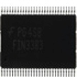
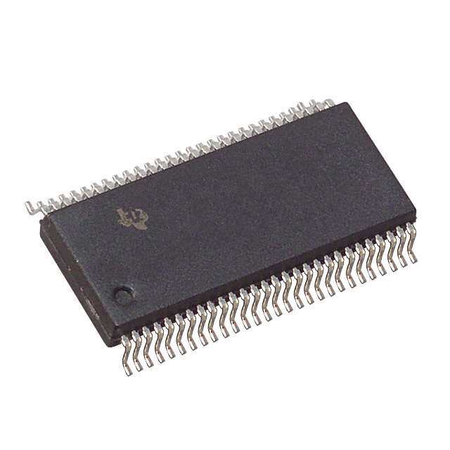
| 描述 | IC SWITCH BUS 24BIT TTL 56TSSOP数字总线开关 IC 24-Bit Bus Switch |
| 产品分类 | |
| 品牌 | Fairchild Semiconductor |
| 产品手册 | |
| 产品图片 |
|
| rohs | 符合RoHS无铅 / 符合限制有害物质指令(RoHS)规范要求 |
| 产品系列 | 开关 IC,数字总线开关 IC,Fairchild Semiconductor FST16211MTD- |
| 数据手册 | |
| 产品型号 | FST16211MTD |
| 产品种类 | 数字总线开关 IC |
| 传播延迟时间 | 0.25 ns at 4 V to 5.5 V |
| 供应商器件封装 | 56-TSSOP |
| 其它名称 | FST16211MTD-ND |
| 包装 | 管件 |
| 单位重量 | 740 mg |
| 商标 | Fairchild Semiconductor |
| 安装类型 | 表面贴装 |
| 安装风格 | SMD/SMT |
| 导通电阻—最大值 | 11 Ohms |
| 封装 | Tube |
| 封装/外壳 | 56-TFSOP(0.240",6.10mm 宽) |
| 封装/箱体 | TSSOP-56 |
| 工作温度 | -40°C ~ 85°C |
| 工厂包装数量 | 34 |
| 开关数量 | Dual |
| 最大工作温度 | + 85 C |
| 最小工作温度 | - 40 C |
| 标准包装 | 34 |
| 独立电路 | 2 |
| 电压-电源 | 4 V ~ 5.5 V |
| 电压源 | 单电源 |
| 电流-输出高,低 | - |
| 电源电压-最大 | 5.5 V |
| 电源电压-最小 | 4 V |
| 电路 | 12 x 1:1 |
| 类型 | FET 总线开关 |
| 系列 | FST16211 |
| 逻辑系列 | FST |


- 商务部:美国ITC正式对集成电路等产品启动337调查
- 曝三星4nm工艺存在良率问题 高通将骁龙8 Gen1或转产台积电
- 太阳诱电将投资9.5亿元在常州建新厂生产MLCC 预计2023年完工
- 英特尔发布欧洲新工厂建设计划 深化IDM 2.0 战略
- 台积电先进制程称霸业界 有大客户加持明年业绩稳了
- 达到5530亿美元!SIA预计今年全球半导体销售额将创下新高
- 英特尔拟将自动驾驶子公司Mobileye上市 估值或超500亿美元
- 三星加码芯片和SET,合并消费电子和移动部门,撤换高东真等 CEO
- 三星电子宣布重大人事变动 还合并消费电子和移动部门
- 海关总署:前11个月进口集成电路产品价值2.52万亿元 增长14.8%


PDF Datasheet 数据手册内容提取
Is Now Part of To learn more about ON Semiconductor, please visit our website at www.onsemi.com Please note: As part of the Fairchild Semiconductor integration, some of the Fairchild orderable part numbers will need to change in order to meet ON Semiconductor’s system requirements. Since the ON Semiconductor product management systems do not have the ability to manage part nomenclature that utilizes an underscore (_), the underscore (_) in the Fairchild part numbers will be changed to a dash (-). This document may contain device numbers with an underscore (_). Please check the ON Semiconductor website to verify the updated device numbers. The most current and up-to-date ordering information can be found at www.onsemi.com. Please email any questions regarding the system integration to Fairchild_questions@onsemi.com. ON Semiconductor and the ON Semiconductor logo are trademarks of Semiconductor Components Industries, LLC dba ON Semiconductor or its subsidiaries in the United States and/or other countries. ON Semiconductor owns the rights to a number of patents, trademarks, copyrights, trade secrets, and other intellectual property. A listing of ON Semiconductor’s product/patent coverage may be accessed at www.onsemi.com/site/pdf/Patent-Marking.pdf. ON Semiconductor reserves the right to make changes without further notice to any products herein. ON Semiconductor makes no warranty, representation or guarantee regarding the suitability of its products for any particular purpose, nor does ON Semiconductor assume any liability arising out of the application or use of any product or circuit, and specifically disclaims any and all liability, including without limitation special, consequential or incidental damages. Buyer is responsible for its products and applications using ON Semiconductor products, including compliance with all laws, regulations and safety requirements or standards, regardless of any support or applications information provided by ON Semiconductor. “Typical” parameters which may be provided in ON Semiconductor data sheets and/or specifications can and do vary in different applications and actual performance may vary over time. All operating parameters, including “Typicals” must be validated for each customer application by customer’s technical experts. ON Semiconductor does not convey any license under its patent rights nor the rights of others. ON Semiconductor products are not designed, intended, or authorized for use as a critical component in life support systems or any FDA Class 3 medical devices or medical devices with a same or similar classification in a foreign jurisdiction or any devices intended for implantation in the human body. Should Buyer purchase or use ON Semiconductor products for any such unintended or unauthorized application, Buyer shall indemnify and hold ON Semiconductor and its officers, employees, subsidiaries, affiliates, and distributors harmless against all claims, costs, damages, and expenses, and reasonable attorney fees arising out of, directly or indirectly, any claim of personal injury or death associated with such unintended or unauthorized use, even if such claim alleges that ON Semiconductor was negligent regarding the design or manufacture of the part. ON Semiconductor is an Equal Opportunity/Affirmative Action Employer. This literature is subject to all applicable copyright laws and is not for resale in any manner.
F July 1997 S T Revised July 2002 1 6 2 1 1 FST16211 2 4 - 24-Bit Bus Switch B it B General Description Features u s The Fairchild Switch FST16211 provides 24-bits of high- (cid:1) 4Ω switch connection between two ports S speed CMOS TTL-compatible bus switching. The low On (cid:1) Minimal propagation delay through the switch w Rouetspiusttas nwceit hoof utth ea dsdwinitcgh parlolopwags aintiopnu tsd etola by eo cro ngneencetreadti ntog (cid:1) Low lCC itc additional ground bounce noise. (cid:1) Zero bounce in flow-through mode h The device is organized as a 12-bit or 24-bit bus switch. (cid:1) Control inputs compatible with TTL level When OE1 is LOW, the switch is ON and Port 1A is con- (cid:1) Also packaged in plastic Fine-Pitch Ball Grid Array nected to Port 1B. When OE2 is LOW, Port 2A is connected (FBGA) to Port 2B. When OE1/2 is HIGH, a high impedance state exists between the A and B Ports. Ordering Code: Order Number Package Number Package Description FST16211G BGA54A 54-Ball Fine-Pitch Ball Grid Array (FBGA), JEDEC MO-205, 5.5mm Wide (Note 1)(Note 2) FST16211MEA MS56A 56-Lead Shrink Small Outline Package (SSOP), JEDEC MO-118, 0.300" Wide (Note 2) FST16211MTD MTD56 56-Lead Thin Shrink Small Outline Package (TSSOP), JEDEC MO-153, 6.1mm Wide (Note 2) Note 1: Ordering code “G” indicates Trays. Note 2: Devices also available in Tape and Reel. Specify by appending the suffix letter “X” to the ordering code. Logic Diagram © 2002 Fairchild Semiconductor Corporation DS500037 www.fairchildsemi.com
1 1 Connection Diagrams Pin Descriptions 2 6 T1 Pin Assignment for SSOP and TSSOP Pin Name Description FS OE1, OE2 Bus Switch Enables 1A, 2A Bus A 1B, 2B Bus B FBGA Pin Assignments 1 2 3 4 5 6 A 1A2 1A1 NC OE2 1B1 1B2 B 1A4 1A3 1A7 OE1 1B3 1B4 C 1A6 1A5 GND 1B7 1B5 1B6 D 1A10 1A9 1A8 1B8 1B9 1B10 E 1A12 1A11 2A1 2B1 1B11 1B12 F 2A4 2A3 2A2 2B2 2B3 2B4 G 2A6 2A5 VCC GND 2B5 2B6 H 2A8 2A7 2A9 2B9 2B7 2B8 J 2A12 2A11 2A10 2B10 2B11 2B12 Truth Table Inputs Inputs/Outputs OE1 OE2 1A, 1B 2A, 2B L L 1A = 1B 2A = 2B L H 1A = 1B Z Pin Assignment for FBGA H L Z 2A = 2B H H Z Z (Top Thru View) www.fairchildsemi.com 2
F Absolute Maximum Ratings Recommended Operating S (Note 3) T Supply Voltage (VCC) −0.5V to +7.0V Conditions (Note 6) 16 DC Switch Voltage (VS) (Note 4) −0.5V to +7.0V Power Supply Operating (VCC) 4.0V to 5.5V 21 DC Input Voltage (VIN) (Note 5) −0.5V to +7.0V Input Voltage (VIN) 0V to 5.5V 1 DC Input Diode Current (lIK) VIN < 0V −50 mA Output Voltage (VOUT) 0V to 5.5V DC Output (IOUT) Sink Current 128 mA Input Rise and Fall Time (tr, tf) DC VCC/GND Current (ICC/IGND) +/− 100 mA Switch Control Input 0 ns/V to 5 ns/V Storage Temperature Range (TSTG) −65°C to +150 °C Switch I/O 0 ns/V to DC Free Air Operating Temperature (TA) -40 °C to +85 °C Note 3: The “Absolute Maximum Ratings” are those values beyond which the safety of the device cannot be guaranteed. The device should not be operated at these limits. The parametric values defined in the Electrical Characteristics tables are not guaranteed at the absolute maximum rating. The “Recommended Operating Conditions” table will define the conditions for actual device operation. Note 4: VS is the voltage observed/applied at either A or B Ports across the switch. Note 5: The input and output negative voltage ratings may be exceeded if the input and output diode current ratings are observed. Note 6: Unused control inputs must be held HIGH or LOW. They may not float. DC Electrical Characteristics Symbol Parameter V(VCC) MiTnA = −40 T°Cyp to +85 °MCax Units Conditions (Note 7) VIK Clamp Diode Voltage 4.5 −1.2 V IIN = −18 mA VIH HIGH Level Input Voltage 4.0–5.5 2.0 V VIL LOW Level Input Voltage 4.0–5.5 0.8 V II Input Leakage Current 5.5 ±1.0 µA 0 ≤ VIN ≤ 5.5V 0 10 µA VIN = 5.5V IOZ OFF-STATE Leakage Current 5.5 ±1.0 µA 0 ≤ A, B ≤ VCC RON Switch On Resistance 4.5 4 7 Ω VIN = 0V, IIN = 64 mA (Note 8) 4.5 4 7 Ω VIN = 0V, IIN = 30 mA 4.5 8 12 Ω VIN = 2.4V, IIN = 15 mA 4.0 11 20 Ω VIN = 2.4V, IIN = 15 mA ICC Quiescent Supply Current 5.5 3 µA VIN = VCC or GND, IOUT = 0 ∆ ICC Increase in ICC per Input 5.5 2.5 mA One Input at 3.4V Other Inputs at VCC or GND Note 7: Typical values are at VCC = 5.0V and TA = +25°C Note 8: Measured by the voltage drop between A and B pins at the indicated current through the switch. On Resistance is determined by the lower of the voltages on the two (A or B) pins. 3 www.fairchildsemi.com
1 1 AC Electrical Characteristics 2 6 T1 TA = −40 °C to +85 °C, S CL = 50pF, RU = RD = 500Ω Figure F Symbol Parameter VCC = 4.5 – 5.5V VCC = 4.0V Units Conditions Number Min Max Min Max tPHL, tPLH Propagation Delay Bus to Bus 0.25 0.25 ns VI = OPEN Figures (Note 9) 1, 2 tPZH, tPZL Output Enable Time 1.5 6.0 6.5 ns VI = 7V for tPZL Figures VI = OPEN for tPZH 1, 2 tPHZ, tPLZ Output Disable Time 1.5 7.0 7.2 ns VI = 7V for tPLZ Figures VI = OPEN for tPHZ 1, 2 Note 9: This parameter is guaranteed by design but is not tested. The bus switch contributes no propagation delay other than the RC delay of the typical On Resistance of the switch and the 50pF load capacitance, when driven by an ideal voltage source (zero output impedance). Capacitance (Note 10) Symbol Parameter Typ Max Units Conditions CIN Control Pin Input Capacitance 3 pF VCC = 5.0V CI/O Input/Output Capacitance 6 pF VCC, OE = 5.0V Note 10: TA = +25°C, f = 1 MHz, Capacitance is characterized but not tested. AC Loading and Waveforms Note: Input driven by 50 Ω source terminated in 50 Ω Note: CL includes load and stray capacitance Note: Input PRR = 1.0 MHz, tW = 500 ns FIGURE 1. AC Test Circuit FIGURE 2. AC Waveforms www.fairchildsemi.com 4
F S T 1 6 2 1 1 54-Ball Fine-Pitch Ball Grid Array (FBGA), JEDEC MO-205, 5.5mm Wide Package Number BGA54A 5 www.fairchildsemi.com
1 1 2 6 1 T S F 56-Lead Shrink Small Outline Package (SSOP), JEDEC MO-118, 0.300" Wide Package Number MS56A www.fairchildsemi.com 6
F S T 1 6 2 1 1 2 4 - B it B u s S w it c h 56-Lead Thin Shrink Small Outline Package (TSSOP), JEDEC MO-153, 6.1mm Wide Package Number MTD56 Technology Description The Fairchild Switch family derives from and embodies Fairchild’s proven switch technology used for several years in its 74LVX3L384 (FST3384) bus switch product. Fairchild does not assume any responsibility for use of any circuitry described, no circuit patent licenses are implied and Fairchild reserves the right at any time without notice to change said circuitry and specifications. LIFE SUPPORT POLICY FAIRCHILD’S PRODUCTS ARE NOT AUTHORIZED FOR USE AS CRITICAL COMPONENTS IN LIFE SUPPORT DEVICES OR SYSTEMS WITHOUT THE EXPRESS WRITTEN APPROVAL OF THE PRESIDENT OF FAIRCHILD SEMICONDUCTOR CORPORATION. As used herein: 1. Life support devices or systems are devices or systems 2. A critical component in any component of a life support which, (a) are intended for surgical implant into the device or system whose failure to perform can be rea- body, or (b) support or sustain life, and (c) whose failure sonably expected to cause the failure of the life support to perform when properly used in accordance with device or system, or to affect its safety or effectiveness. instructions for use provided in the labeling, can be rea- sonably expected to result in a significant injury to the www.fairchildsemi.com user. 7 www.fairchildsemi.com
ON Semiconductor and are trademarks of Semiconductor Components Industries, LLC dba ON Semiconductor or its subsidiaries in the United States and/or other countries. ON Semiconductor owns the rights to a number of patents, trademarks, copyrights, trade secrets, and other intellectual property. A listing of ON Semiconductor’s product/patent coverage may be accessed at www.onsemi.com/site/pdf/Patent−Marking.pdf. ON Semiconductor reserves the right to make changes without further notice to any products herein. ON Semiconductor makes no warranty, representation or guarantee regarding the suitability of its products for any particular purpose, nor does ON Semiconductor assume any liability arising out of the application or use of any product or circuit, and specifically disclaims any and all liability, including without limitation special, consequential or incidental damages. Buyer is responsible for its products and applications using ON Semiconductor products, including compliance with all laws, regulations and safety requirements or standards, regardless of any support or applications information provided by ON Semiconductor. “Typical” parameters which may be provided in ON Semiconductor data sheets and/or specifications can and do vary in different applications and actual performance may vary over time. All operating parameters, including “Typicals” must be validated for each customer application by customer’s technical experts. ON Semiconductor does not convey any license under its patent rights nor the rights of others. ON Semiconductor products are not designed, intended, or authorized for use as a critical component in life support systems or any FDA Class 3 medical devices or medical devices with a same or similar classification in a foreign jurisdiction or any devices intended for implantation in the human body. Should Buyer purchase or use ON Semiconductor products for any such unintended or unauthorized application, Buyer shall indemnify and hold ON Semiconductor and its officers, employees, subsidiaries, affiliates, and distributors harmless against all claims, costs, damages, and expenses, and reasonable attorney fees arising out of, directly or indirectly, any claim of personal injury or death associated with such unintended or unauthorized use, even if such claim alleges that ON Semiconductor was negligent regarding the design or manufacture of the part. ON Semiconductor is an Equal Opportunity/Affirmative Action Employer. This literature is subject to all applicable copyright laws and is not for resale in any manner. PUBLICATION ORDERING INFORMATION LITERATURE FULFILLMENT: N. American Technical Support: 800−282−9855 Toll Free ON Semiconductor Website: www.onsemi.com Literature Distribution Center for ON Semiconductor USA/Canada 19521 E. 32nd Pkwy, Aurora, Colorado 80011 USA Europe, Middle East and Africa Technical Support: Order Literature: http://www.onsemi.com/orderlit Phone: 303−675−2175 or 800−344−3860 Toll Free USA/Canada Phone: 421 33 790 2910 Fax: 303−675−2176 or 800−344−3867 Toll Free USA/Canada Japan Customer Focus Center For additional information, please contact your local Email: orderlit@onsemi.com Phone: 81−3−5817−1050 Sales Representative © Semiconductor Components Industries, LLC www.onsemi.com www.onsemi.com 1