 Datasheet下载
- 型号: FSA8009UMX
- 制造商: Fairchild Semiconductor
- 库位|库存: xxxx|xxxx
- 要求:
| 数量阶梯 | 香港交货 | 国内含税 |
| +xxxx | $xxxx | ¥xxxx |
查看当月历史价格
查看今年历史价格
FSA8009UMX产品简介:
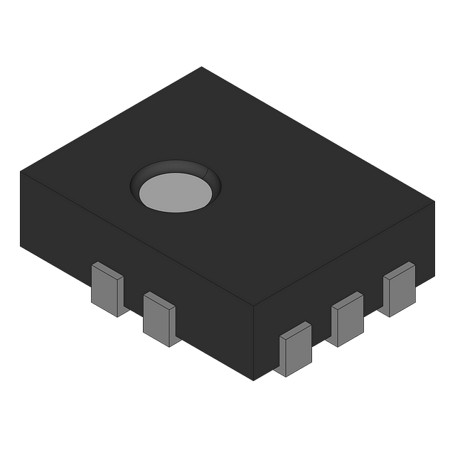
ICGOO电子元器件商城为您提供FSA8009UMX由Fairchild Semiconductor设计生产,在icgoo商城现货销售,并且可以通过原厂、代理商等渠道进行代购。 FSA8009UMX价格参考。Fairchild SemiconductorFSA8009UMX封装/规格:音频专用, Audio Detection Switch 1 Channel 10-UMLP (1.8x1.4)。您可以下载FSA8009UMX参考资料、Datasheet数据手册功能说明书,资料中有FSA8009UMX 详细功能的应用电路图电压和使用方法及教程。
FSA8009UMX是安森美(ON Semiconductor)推出的一款音频专用开关芯片,主要应用于便携式消费类电子产品中。其典型应用场景包括智能手机、平板电脑、笔记本电脑及多媒体播放器等设备的音频信号切换与检测。

该芯片集成了音频插孔检测功能,可自动识别插入的3.5mm耳机或带有麦克风的四段式耳机(TRRS),并根据设备接口标准(如CTIA或OMTP)进行智能配置,确保耳机麦克风和立体声输出正常工作。同时,FSA8009UMX支持音频路径切换,可在内置扬声器、耳机、麦克风之间实现无缝切换,提升用户体验。

此外,该器件具备低功耗特性,适合电池供电设备;采用微型封装(如UCSP),节省PCB空间,适用于高密度布局的移动终端。其高集成度和高可靠性使其成为现代智能设备中音频子系统的关键组件。
| 参数 | 数值 |
| 产品目录 | 集成电路 (IC)半导体 |
| 描述 | IC AUDIO JACK DETECTOR/SW 10UMLP开关 IC - 各种 Audio Jack Send/End Detection/Video Swth |
| 产品分类 | 线性 - 音频处理集成电路 - IC |
| 品牌 | Fairchild Semiconductor |
| 产品手册 | |
| 产品图片 |
|
| rohs | 符合RoHS无铅 / 符合限制有害物质指令(RoHS)规范要求 |
| 产品系列 | 开关 IC,开关 IC - 各种,Fairchild Semiconductor FSA8009UMX- |
| 数据手册 | |
| 产品型号 | FSA8009UMX |
| PCN设计/规格 | |
| 产品种类 | 开关 IC - 各种 |
| 供应商器件封装 | 10-UMLP (1.8x1.4) |
| 其它名称 | FSA8009UMXDKR |
| 包装 | Digi-Reel® |
| 单位重量 | 40 mg |
| 商标 | Fairchild Semiconductor |
| 安装类型 | 表面贴装 |
| 安装风格 | SMD/SMT |
| 封装 | Reel |
| 封装/外壳 | 10-UFQFN |
| 封装/箱体 | UMLP-10 |
| 工厂包装数量 | 5000 |
| 应用 | MP3 播放器,便携式媒体播放器 |
| 开关数量 | Single |
| 开关配置 | SPST |
| 最大工作温度 | + 85 C |
| 最小工作温度 | - 40 C |
| 标准包装 | 1 |
| 电源电压-最大 | 4.3 V |
| 电源电压-最小 | 2.5 V |
| 类型 | 音频插孔探测器,带视频开关 |
| 系列 | FSA8009 |


- 商务部:美国ITC正式对集成电路等产品启动337调查
- 曝三星4nm工艺存在良率问题 高通将骁龙8 Gen1或转产台积电
- 太阳诱电将投资9.5亿元在常州建新厂生产MLCC 预计2023年完工
- 英特尔发布欧洲新工厂建设计划 深化IDM 2.0 战略
- 台积电先进制程称霸业界 有大客户加持明年业绩稳了
- 达到5530亿美元!SIA预计今年全球半导体销售额将创下新高
- 英特尔拟将自动驾驶子公司Mobileye上市 估值或超500亿美元
- 三星加码芯片和SET,合并消费电子和移动部门,撤换高东真等 CEO
- 三星电子宣布重大人事变动 还合并消费电子和移动部门
- 海关总署:前11个月进口集成电路产品价值2.52万亿元 增长14.8%


PDF Datasheet 数据手册内容提取
Is Now Part of To learn more about ON Semiconductor, please visit our website at www.onsemi.com Please note: As part of the Fairchild Semiconductor integration, some of the Fairchild orderable part numbers will need to change in order to meet ON Semiconductor’s system requirements. Since the ON Semiconductor product management systems do not have the ability to manage part nomenclature that utilizes an underscore (_), the underscore (_) in the Fairchild part numbers will be changed to a dash (-). This document may contain device numbers with an underscore (_). Please check the ON Semiconductor website to verify the updated device numbers. The most current and up-to-date ordering information can be found at www.onsemi.com. Please email any questions regarding the system integration to Fairchild_questions@onsemi.com. ON Semiconductor and the ON Semiconductor logo are trademarks of Semiconductor Components Industries, LLC dba ON Semiconductor or its subsidiaries in the United States and/or other countries. ON Semiconductor owns the rights to a number of patents, trademarks, copyrights, trade secrets, and other intellectual property. A listing of ON Semiconductor’s product/patent coverage may be accessed at www.onsemi.com/site/pdf/Patent-Marking.pdf. ON Semiconductor reserves the right to make changes without further notice to any products herein. ON Semiconductor makes no warranty, representation or guarantee regarding the suitability of its products for any particular purpose, nor does ON Semiconductor assume any liability arising out of the application or use of any product or circuit, and specifically disclaims any and all liability, including without limitation special, consequential or incidental damages. Buyer is responsible for its products and applications using ON Semiconductor products, including compliance with all laws, regulations and safety requirements or standards, regardless of any support or applications information provided by ON Semiconductor. “Typical” parameters which may be provided in ON Semiconductor data sheets and/or specifications can and do vary in different applications and actual performance may vary over time. All operating parameters, including “Typicals” must be validated for each customer application by customer’s technical experts. ON Semiconductor does not convey any license under its patent rights nor the rights of others. ON Semiconductor products are not designed, intended, or authorized for use as a critical component in life support systems or any FDA Class 3 medical devices or medical devices with a same or similar classification in a foreign jurisdiction or any devices intended for implantation in the human body. Should Buyer purchase or use ON Semiconductor products for any such unintended or unauthorized application, Buyer shall indemnify and hold ON Semiconductor and its officers, employees, subsidiaries, affiliates, and distributors harmless against all claims, costs, damages, and expenses, and reasonable attorney fees arising out of, directly or indirectly, any claim of personal injury or death associated with such unintended or unauthorized use, even if such claim alleges that ON Semiconductor was negligent regarding the design or manufacture of the part. ON Semiconductor is an Equal Opportunity/Affirmative Action Employer. This literature is subject to all applicable copyright laws and is not for resale in any manner.
F S A 8 0 March 2013 0 9 – A u FSA8009 d i o Audio Jack Send / End Detection with MIC / Video Switch J a c k Features Description S e The FSA8009 is an audio jack microphone / video switch for n Accessory Plug-In d Detection 3- or 4-Pole Audio Jack 3- or 4-pole accessories with send / end (S/E) detection. In / addition to detection, the FSA8009 features an integrated E Send / End Key Pressed microphone / video switch that allows the processor to n Switch Type Microphone & Video configure the audio jack. The architecture is designed to d V 2.5 to 4.3 V allow common third-party headphones to be used for D DD e THD (MIC) 0.01% Typical listening to music from mobile handsets, personal media te players, and portable peripheral devices. c ESD (Air Gap) 16 kV t Operating Temperature -40°C to 85°C Determines When Send / End Button Key is Pressed io n 10-Lead UMLP Integrates a MIC / Video Switch for 4-Pole Configuration w Package 1.4x1.8x0.5 mm, 0.4 mm Reduces Pop / Click Caused by Microphone Bias it Pitch h M Top Mark KP Related Resources I C Ordering Information FSA8009UMX For samples and questions, please contact: / V Analog.Switch@fairchildsemi.com. Applications id FSA8009 Demonstration Board e o 3.5 mm and 2.5 mm Audio Jacks S Cellular Phones, Smartphones w MP3 and PMP it c h Typical Application Baseband Processor GPIO VIO 2.8V VIO VDD 10KΩ R_VDD TTL Level Input EN Enable GPIO1 Open Drain OutputS/E GPIO2 TTL Level InputSEL L R GND MIC GPIO3 + REF 1 2 3 4 Audio - CODEC R MIC MIC MIC Bias y e L SPKMRIC CMIC VID J_MIC 2Ω 2Ω C, S/E K R SPKR GND 16-3 16-3 N Applications Processor Video Out Figure 1. Mobile Phone Example © 2010 Fairchild Semiconductor Corporation www.fairchildsemi.com FSA8009 • Rev. 1.0.2
F S A 8 Pin Descriptions 0 0 9 Name Pin # Type Description – A u R_VDD 1 Output Optional pull-up voltage, with a resistor divider, sets the reference voltage on the REF pin d i o 0 Device inactive(1) J EN 2 Input Device enable, low-power mode a 1 Device active(1) c k 0 VID = J_MIC(1) S SEL 3 Input MIC / VID switch select pin e 1 MIC = J_MIC(1) n d Indicates state of send /end key press, open-drain output requires 0 Press(1) / S/E 4 Output E pull-up resistor 1 No key press(1) n d VID 6 Switch Video switch path; connects between video source and audio jack microphone pin D VDD 5 Power Supply voltage e t e MIC 7 Switch Microphone switch path that goes to the CODEC microphone amplifier input c t J_MIC 8 Switch Microphone switch path that connects to the microphone, SEND/END key, and jack pole video io n Reference voltage used to detect a send / end key press, through a resistor divider off R_VDD or REF 10 Input w external voltage reference i t h GND 9 Ground Ground for both the audio jack and the PCB M Note: I C 1. 0 = VOL or VIL; 1 = VOH or VIH. / V i d EN R_VDD e o S w 2 1 it SEL 3 10 REF ch S/E 4 9 GND VDD 5 8 J_MIC 6 7 VID MIC Figure 2. UMLP Pin Assignment (Through View) Table 1. Device Configuration in Reset and Active States EN SEL MIC VID R_VDD S/E 0 X 3-State 3-State GND HIGH 1 1 J_MIC Open VDD Active 1 0 Open J_MIC GND LOW © 2010 Fairchild Semiconductor Corporation www.fairchildsemi.com FSA8009 • Rev. 1.0.2 2
F S A Absolute Maximum Ratings 8 0 0 Stresses exceeding the absolute maximum ratings may damage the device. The device may not function or be operable 9 above the recommended operating conditions and stressing the parts to these levels is not recommended. In addition, – extended exposure to stresses above the recommended operating conditions may affect device reliability. The absolute A u maximum ratings are stress ratings only. d i o Symbol Parameter Min. Max. Units J a VDD Supply Voltage from Battery -0.5 5.5 V c k VSW Switch I/O Voltage -0.5 VDD+0.5 V S I Input Clamp Diode Current(2) -50 mA e IK n I Switch I/O Current (Continuous)(2) 50 mA d SW / T Storage Temperature Range -65 +150 °C E STG n T Maximum Junction Temperature +150 °C d J D TL Lead Temperature (Soldering, 10 Seconds) +260 °C e t Air Gap 16 e c IEC 61000-4-2 System t Contact 10 i o n ESD All other Pins 6 kV w Human Body Model, JEDEC JESD22-A114 VJ_D, EGTN, DJ_ MIC, VDD, 8 ith IO M Charged Device Model, JEDEC JESD22-C101 All Pins 2 I C Note: / 2. The input and output negative ratings may be exceeded if the input and output diode current ratings are observed. V i d e o S w Recommended Operating Conditions i t c The Recommended Operating Conditions table defines the conditions for actual device operation. Recommended operating h conditions are specified to ensure optimal performance to the datasheet specifications. Fairchild does not recommend exceeding them or designing to Absolute Maximum Ratings. Symbol Parameter Min. Max. Units V Battery Supply Voltage 2.5 4.3 V DD T Operating Temperature -40 +85 ºC A © 2010 Fairchild Semiconductor Corporation www.fairchildsemi.com FSA8009 • Rev. 1.0.2 3
F S A 8 DC Electrical Characteristics 0 0 9 All typical values are at TA=25°C unless otherwise specified. – MIC Switch A u d T = -40 to +85°C Symbol Parameter V (V) Conditions A Units io DD Min. Typ. Max. J a c 2.8 2.0 4.0 k 3.0 1.5 3.5 S R MIC Switch On Resistance I = 24 mA, V = 2.2 V Ω e ON 3.3 OUT IN 1.2 3.0 n d 3.8 1.0 2.5 / E 2.8 0.7 1.5 n d R On Resistance Flatness 3.0 IOUT = 24 mA, 0.6 1.4 Ω D FLAT(ON) 3.3 VIN = 1 V to VDD 0.5 1.3 e t e 3.8 0.5 1.2 c t i V Switch Input Voltage Range 2.5 to 4.3 0 V V o IN DD n C MIC and J_MIC Switch ON 2.8 f = 1 MHz 15 pF w ON Capacitance i t h MIC and J_MIC Switch OFF C 2.8 f = 1 MHz 8 pF M OFF Capacitance I C / V Video Switch Characteristics i d e T = -40 to +85°C o Symbol Parameter VDD (V) Conditions A Unit S Min. Typ. Max. w i t 2.8 1.0 1.5 c h 3.0 0.9 1.4 R MIC Switch On Resistance I = 24 mA, V = 0.5 V Ω ON OUT IN 3.3 0.8 1.3 3.8 0.7 1.2 2.8 0.4 0.60 3.0 I = 24 mA, V = 0 V to 0.3 0.55 R On Resistance Flatness OUT IN Ω FLAT(ON) 3.3 1.2 V 0.2 0.50 3.8 0.15 0.45 V Switch Input Voltage Range 2.5 to 4.3 0 1.5 V IN C VID Switch ON Capacitance 2.8 f = 1 MHz 40 pF ON C VID Switch OFF Capacitance 2.8 f = 1 MHz 10 pF OFF Parallel I/O T = -40 to +85°C A Symbol Parameter Unit Min. Typ. Max. V Input High Voltage (EN, SEL) 0.44 x V V V IH DD DD V Input Low Voltage (EN, SEL) GND 0.15 x V V IL DD PUR Pull-Up Resistor on S/E 2 110 KΩ S/E V Output Low Voltage (S/E) (V = Voltage of Pull-Up Resistor) 0.2 x V V OL PUR PUR © 2010 Fairchild Semiconductor Corporation www.fairchildsemi.com FSA8009 • Rev. 1.0.2 4
F S A 8 DC Electrical Characteristics (Continued) 0 0 9 All typical values are at TA=25°C unless otherwise specified. – Comparator NC Switch A u d T = -40 to +85°C Symbol Parameter V (V) Conditions A Unit io DD Min. Typ. Max. J a c V Input Voltage on REF Pin 1 VDD – V k REF 0.075 S e COMHYS Hysteresis of Comparator "-” Terminal 50 mV n d / E Current n d D T = -40 to +85°C A e Symbol Parameter VDD (V) Conditions Min. Typ. Max. Unit te c t J_MIC = 1 V, 4.3 V io I Off-State Leakage Current 4.3 -15 15 nA OFF MIC or VID = 4.3 V, 1 V n w I Input Leakage Current 0 to 4.3 Inputs 0 to 4.3 V 1 µA IN i t h ICC-EN Low-Power Mode 2.5 to 4.3 EN = LOW 10 nA M Active Current I I Current during Video Mode 2.5 to 4.3 10 nA C CC-VID (EN = HIGH, SEL = LOW) / Active Current V ICC-MIC Current during Microphone Mode 2.5 to 4.3 (EN = HIGH, SEL = HIGH) 20 µA id e o S w i t c h © 2010 Fairchild Semiconductor Corporation www.fairchildsemi.com FSA8009 • Rev. 1.0.2 5
F S A 8 0 0 9 AC Electrical Characteristics – A All typical values are for VCC=3.3 V at TA=25°C unless otherwise specified. u d MIC Switch io J T = -40 to +85°C a A c Symbol Parameter V (V) Conditions Unit DD k Min. Typ. Max. S e THD Total Harmonic Distortion 2.8 RT = 600 Ω, VSW = 0.5 VPP, .003 % n f = 20 Hz to 20 kHz, V = 2.2 V d IN / O Off Isolation 2.8 f = 20 kHz, RS=32 Ω, CL=0 pF, -100 dB E IRR R =32 Ω n T d XTALK Crosstalk from MIC to VID 2.8 f = 100 MHz, RL=100 Ω -67 dB D e t Video Switch Characteristics e c t TA = -40 to +85°C io Symbol Parameter V (V) Conditions Unit n DD Min. Typ. Max. w i DG Differential Gain 2.8 RL = 150 Ω, f = 3.58 MHz .09 % th M D Differential Phase 2.8 R = 150 Ω, f = 3.58 MHz .13 ◦ P L I C O Off Isolation 2.8 f=10 MHz, R =150 Ω, -45 dB IRR L / f=10 MHz, R = 10 Ω, C =0 pF, V XTALK Crosstalk from VID to MIC 2.8 R =150 Ω IN L -65 dB id L e o Parallel I/O S w Symbol Parameter VDD (V) Conditions TA = -40 to +85°C Unit itc Min. Typ. Max. h t Break-Before-Make Time 2.5 to 4.3 120 ns BBM EN LOW HIGH or EN t Enable or Disable Time 2.5 to 4.3 15 µs EN HIGHLOW SEL LOW HIGH to Comparator t Select to Comparator On 2.5 to 4.3 10 µs SEL-COM-ON ON SEL HIGHLOW to Comparator t Select to Comparator Off 2.5 to 4.3 20 ns SEL-COM-OFF OFF t Switch Turn-On Time 2.5 to 4.3 40 ns ON t Switch Turn-Off Time 2.5 to 4.3 15 ns OFF Propagation Delay from J_MIC > REF from LOWHIGH t Comparator Trigger to S/E 2.5 to 4.3 10 µs J_MIC-S/E J_MIC < REF from HIGHLOW Output Power T = -40 to +85°C A Symbol Parameter V (V) Conditions Unit DD Min. Typ. Max. Power Supply Noise 300 mV , PSRR Power Supply Rejection Ratio 2.8 PP -100 dB Measured 10/90%, f=217 Hz © 2010 Fairchild Semiconductor Corporation www.fairchildsemi.com FSA8009 • Rev. 1.0.2 6
F S A 8 Physical Dimensions 0 0 9 0.10 C 1.40 A – B A 2X 1.70 (9X) u d 0.663 0.563 io J 1.80 a 1 c k PIN#1 IDENT 2.10 S e 0.10 C 0.40 n TOP VIEW d 2X / (10X)0.225 E n 0.10 C 0.55 MAX. (0.15) RLEACNODM PMATETNEDREND d D e 1.45 9X te 0.080C.05 SEATING C 0.55 0.45 cti 0.00 PLANE o n SIDE VIEW w 0.40 i t h 1.85 0.35 M (9X) 0.45 I C 3 (10X)0.225 / 0.40 OPTIONAL MINIMIAL V i 6 TOE LAND PATTERN d DETAIL A e o 1 NOTES: S PIN#1 IDENT w 10 0.15(10X) A . APNAYC KJAEGDEEC D SOTEASN NDOATR DC.ONFORM TO itc 0.25 h B. DIMENSIONS ARE IN MILLIMETERS. 0.10 C A B BOTTOM VIEW C. DIMENSIONS AND TOLERANCES PER 0.05 C ASME Y14.5M, 1994. D. LAND PATTERN RECOMMENDATION IS 0.55 BASED ON FSC DESIGN ONLY. 0.45 PACKAGE E. DRAWING FILENAME: MKT-UMLP10Arev5. EDGE F. FAIRCHILD SEMICONDUCTOR. 45° LEAD LEAD 0.25 OPTION 1 OPTION 2 0.15 DETAIL A SCALE : 2X SCALE : 2X SCALE : 2X Figure 3. 10-Lead UMLP Package Drawing Package drawings are provided as a service to customers considering Fairchild components. Drawings may change in any manner without notice. Please note the revision and/or date on the drawing and contact a Fairchild Semiconductor representative to verify or obtain the most recent revision. Package specifications do not expand the terms of Fairchild’s worldwide terms and conditions, specifically the warranty therein, which covers Fairchild products. Always visit Fairchild Semiconductor’s online packaging area for the most recent package drawings: http://www.fairchildsemi.com/packaging/. Ordering Information Part Number Operating Temperature Range Top Mark Package 10-Lead 1.4 x 1.8 x 0.55 mm, 0.4 mm Pitch, FSA8009UMX -40 to +85°C KP Ultrathin Molded Leadless Package (UMLP) © 2010 Fairchild Semiconductor Corporation www.fairchildsemi.com FSA8009 • Rev. 1.0.2 7
F S A 8 0 0 9 – A u d i o J a c k S e n d / E n d D e t e c t i o n w i t h M I C / V i d e o S w i t c h © 2010 Fairchild Semiconductor Corporation www.fairchildsemi.com FSA8009 • Rev. 1.0.2 8
ON Semiconductor and are trademarks of Semiconductor Components Industries, LLC dba ON Semiconductor or its subsidiaries in the United States and/or other countries. ON Semiconductor owns the rights to a number of patents, trademarks, copyrights, trade secrets, and other intellectual property. A listing of ON Semiconductor’s product/patent coverage may be accessed at www.onsemi.com/site/pdf/Patent−Marking.pdf. ON Semiconductor reserves the right to make changes without further notice to any products herein. ON Semiconductor makes no warranty, representation or guarantee regarding the suitability of its products for any particular purpose, nor does ON Semiconductor assume any liability arising out of the application or use of any product or circuit, and specifically disclaims any and all liability, including without limitation special, consequential or incidental damages. Buyer is responsible for its products and applications using ON Semiconductor products, including compliance with all laws, regulations and safety requirements or standards, regardless of any support or applications information provided by ON Semiconductor. “Typical” parameters which may be provided in ON Semiconductor data sheets and/or specifications can and do vary in different applications and actual performance may vary over time. All operating parameters, including “Typicals” must be validated for each customer application by customer’s technical experts. ON Semiconductor does not convey any license under its patent rights nor the rights of others. ON Semiconductor products are not designed, intended, or authorized for use as a critical component in life support systems or any FDA Class 3 medical devices or medical devices with a same or similar classification in a foreign jurisdiction or any devices intended for implantation in the human body. Should Buyer purchase or use ON Semiconductor products for any such unintended or unauthorized application, Buyer shall indemnify and hold ON Semiconductor and its officers, employees, subsidiaries, affiliates, and distributors harmless against all claims, costs, damages, and expenses, and reasonable attorney fees arising out of, directly or indirectly, any claim of personal injury or death associated with such unintended or unauthorized use, even if such claim alleges that ON Semiconductor was negligent regarding the design or manufacture of the part. ON Semiconductor is an Equal Opportunity/Affirmative Action Employer. This literature is subject to all applicable copyright laws and is not for resale in any manner. PUBLICATION ORDERING INFORMATION LITERATURE FULFILLMENT: N. American Technical Support: 800−282−9855 Toll Free ON Semiconductor Website: www.onsemi.com Literature Distribution Center for ON Semiconductor USA/Canada 19521 E. 32nd Pkwy, Aurora, Colorado 80011 USA Europe, Middle East and Africa Technical Support: Order Literature: http://www.onsemi.com/orderlit Phone: 303−675−2175 or 800−344−3860 Toll Free USA/Canada Phone: 421 33 790 2910 Fax: 303−675−2176 or 800−344−3867 Toll Free USA/Canada Japan Customer Focus Center For additional information, please contact your local Email: orderlit@onsemi.com Phone: 81−3−5817−1050 Sales Representative © Semiconductor Components Industries, LLC www.onsemi.com www.onsemi.com 1