 Datasheet下载
- 型号: SRC4382IPFB
- 制造商: Texas Instruments
- 库位|库存: xxxx|xxxx
- 要求:
| 数量阶梯 | 香港交货 | 国内含税 |
| +xxxx | $xxxx | ¥xxxx |
查看当月历史价格
查看今年历史价格
SRC4382IPFB产品简介:
ICGOO电子元器件商城为您提供SRC4382IPFB由Texas Instruments设计生产,在icgoo商城现货销售,并且可以通过原厂、代理商等渠道进行代购。 SRC4382IPFB价格参考¥56.53-¥88.56。Texas InstrumentsSRC4382IPFB封装/规格:音频专用, Audio Sample Rate Converter 2 Channel 48-TQFP (7x7)。您可以下载SRC4382IPFB参考资料、Datasheet数据手册功能说明书,资料中有SRC4382IPFB 详细功能的应用电路图电压和使用方法及教程。
Texas Instruments(德州仪器)的SRC4382IPFB是一款音频专用的多通道同步采样率转换器(Sample Rate Converter, SRC)。它主要应用于需要高质量音频处理和多通道音频信号同步的场景。以下是其典型应用场景:

 1. 家庭影院与AV接收器
   - 在家庭影院系统中,SRC4382IPFB用于将不同来源的音频信号(如蓝光播放器、流媒体设备、游戏机等)统一转换为相同的采样率,确保音频信号在多声道系统中同步输出。
   - 支持高达8通道的音频处理,适用于Dolby Atmos或DTS:X等沉浸式音频格式。

 2. 专业音频设备
   - 用于调音台、音频接口或其他专业音频设备中,实现多路音频输入/输出之间的采样率匹配。
   - 提供高精度的采样率转换,减少抖动和失真,保证音频质量。

 3. 汽车音响系统
   - 在高端汽车音响中,SRC4382IPFB负责将来自不同源(如蓝牙、USB、CD等)的音频信号转换为一致的采样率,优化车内音频体验。
   - 支持多通道音频处理,满足现代车载娱乐系统的复杂需求。

 4. 便携式音频设备
   - 应用于便携式音频播放器、耳机放大器或DAC(数字模拟转换器),提供高质量的音频重采样功能。
   - 确保不同音频文件格式的采样率差异不会影响最终的音质表现。

 5. 广播与录音设备
   - 在广播系统或录音棚中,SRC4382IPFB用于处理多通道音频信号的同步和采样率转换,确保录制和播放的一致性。
   - 其低延迟特性适合实时音频处理应用。

 6. 物联网(IoT)音频设备
   - 在智能音箱、语音助手等IoT设备中,SRC4382IPFB可以处理来自云端或本地的音频信号,支持多种采样率的无缝切换。
   - 提供高效的音频处理能力,同时降低功耗。

 核心优势
- 多通道支持:支持最多8通道音频信号的同步采样率转换。
- 高精度转换:提供高质量的音频重采样,减少失真和噪声。
- 灵活性强:支持多种输入和输出采样率配置,适应不同应用场景。
- 低延迟:确保实时音频处理的流畅性。

综上所述,SRC4382IPFB广泛应用于需要高质量音频处理和多通道同步的场景,特别是在家庭影院、专业音频设备、汽车音响以及便携式音频设备等领域表现出色。
| 参数 | 数值 |
| 产品目录 | 集成电路 (IC)半导体 |
| 描述 | IC SAMPLE RATE CONV 2CH 48-TQFP音频采样频率转换器 Combo Sample Rate Converter |
| DevelopmentKit | SRC4382EVM-PDK |
| 产品分类 | 线性 - 音频处理集成电路 - IC |
| 品牌 | Texas Instruments |
| 产品手册 | |
| 产品图片 |
|
| rohs | 符合RoHS无铅 / 符合限制有害物质指令(RoHS)规范要求 |
| 产品系列 | 音频 IC,音频采样频率转换器,Texas Instruments SRC4382IPFB- |
| 数据手册 | |
| 产品型号 | SRC4382IPFB |
| THD+噪声 | - 125 dB |
| 产品目录页面 | |
| 产品种类 | 音频采样频率转换器 |
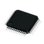
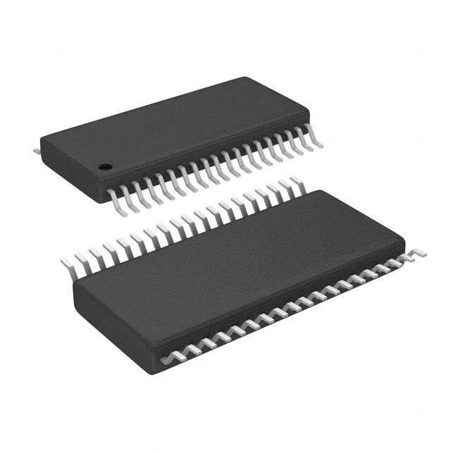
| 供应商器件封装 | 48-TQFP(7x7) |
| 其它名称 | 296-26675 |
| 功率耗散 | 326 mW |
| 包装 | 托盘 |
| 单位重量 | 140 mg |
| 商标 | Texas Instruments |
| 安装类型 | 表面贴装 |
| 安装风格 | SMD/SMT |
| 封装 | Tray |
| 封装/外壳 | 48-TQFP |
| 封装/箱体 | TQFP-48 |
| 工作温度范围 | - 40 C to + 85 C |
| 工作电源电压 | 1.65 V to 2 V / 3 V to 3.6 V |
| 工厂包装数量 | 250 |
| 应用 | 接口,记录器,路由器 |
| 接口 | I2C, SPI |
| 标准包装 | 250 |
| 类型 | 采样率转换器 |
| 系列 | SRC4382 |
| 配用 | /product-detail/zh/SRC4382EVM-PDK/SRC4382EVM-PDK-ND/1595141 |


PDF Datasheet 数据手册内容提取
(cid:2)(cid:17)(cid:14)(cid:14)(cid:20)(cid:2)(cid:14)(cid:13)(cid:18)(cid:12) (cid:4)(cid:14)(cid:13)(cid:8)(cid:17)(cid:7)(cid:16)(cid:15) (cid:10)(cid:14)(cid:13)(cid:11) (cid:5)(cid:9)(cid:19)(cid:6)(cid:15) (cid:3)(cid:12)(cid:15)(cid:16)(cid:14)(cid:17)(cid:11)(cid:9)(cid:12)(cid:16)(cid:15) SRC4382 SRC4382 SBFS030C–JANUARY2006–REVISEDSEPTEMBER2007 Two-Channel, Asynchronous Sample Rate Converter with Integrated Digital Audio Interface Receiver and Transmitter FEATURES • DigitalAudioInterfaceReceiver(DIR) 1 • Two-ChannelAsynchronousSampleRate – PLLLockRangeIncludesSamplingRates 234 Converter(SRC) from20kHzto216kHz – DynamicRangewith–60dBInput – IncludesFourDifferentialInputLine (A-Weighted):128dBtypical ReceiversandanInputMultiplexer – TotalHarmonicDistortionandNoise – BypassMultiplexerRoutesLineReceiver (THD+N)withFull-ScaleInput:–125dB OutputstoLineDriverandBufferOutputs typical – Block-SizedDataBuffersforBothChannel – SupportsAudioInputandOutputData StatusandUserData WordLengthsUpto24Bits – AutomaticDetectionofNon-PCMAudio – SupportsInputandOutputSampling Streams(DTSCD/LDandIEC61937 FrequenciesUpto216kHz formats) – AutomaticDetectionoftheInput-to-Output – AudioCDQ-ChannelSub-CodeDecoding SamplingRatio andDataBuffer – WideInput-to-OutputConversionRange: – StatusRegistersandInterruptGeneration 16:1to1:16Continuous forFlagandErrorConditions – ExcellentJitterAttenuationCharacteristics – LowJitterRecoveredClockOutput – DigitalDe-EmphasisFilteringfor32kHz, • TwoAudioSerialPorts(PortsAandB) 44.1kHz,and48kHzInputSamplingRates – SynchronousSerialInterfacetoExternal – DigitalOutputAttenuationandMute SignalProcessors,DataConverters,and Functions Logic – OutputWordLengthReduction – SlaveorMasterModeOperationwith – StatusRegistersandInterruptGeneration SamplingRatesupto216kHz forSamplingRatioandReadyFlags – SupportsLeft-Justified,Right-Justified,and • DigitalAudioInterfaceTransmitter(DIT) PhilipsI2S™DataFormats – SupportsSamplingRatesUpto216kHz – SupportsAudioDataWordLengthsUpto 24Bits – IncludesDifferentialLineDriverand CMOSBufferedOutputs • FourGeneral-PurposeDigitalOutputs – Block-SizedDataBuffersforBothChannel – MultifunctionProgrammableViaControl StatusandUserData Registers – StatusRegistersandInterruptGeneration • ExtensivePower-DownSupport forFlagandErrorConditions – FunctionalBlocksMayBeDisabled • User-SelectableSerialHostInterface:SPIor IndividuallyWhenNotInUse PhilipsI2C™ • OperatesFrom+1.8VCoreand+3.3VI/O – ProvidesAccesstoOn-ChipRegistersand PowerSupplies DataBuffers • SmallTQFP-48Package,Compatiblewiththe SRC4392andDIX4192 U.S.PatentNo.7,262,716 1 Pleasebeawarethatanimportantnoticeconcerningavailability,standardwarranty,anduseincriticalapplicationsof TexasInstrumentssemiconductorproductsanddisclaimerstheretoappearsattheendofthisdatasheet. DolbyisaregisteredtrademarkofDolbyLaboratories. 2 I2C,I2SaretrademarksofKoninklijkePhilipsElectronicsN.V. 3 Allothertrademarksarethepropertyoftheirrespectiveowners. 4 PRODUCTIONDATAinformationiscurrentasofpublicationdate. Copyright©2006–2007,TexasInstrumentsIncorporated Products conform to specifications per the terms of the Texas Instruments standard warranty. Production processing does not necessarilyincludetestingofallparameters.
SRC4382 www.ti.com SBFS030C–JANUARY2006–REVISEDSEPTEMBER2007 APPLICATIONS DESCRIPTION • DIGITALAUDIORECORDERSAND The SRC4382 is a highly-integrated CMOS device MIXINGDESKS designed for use in professional and broadcast digital • DIGITALAUDIOINTERFACESFOR audio systems. The SRC4382 combines a COMPUTERS high-performance, two-channel, asynchronous • DIGITALAUDIOROUTERSAND sample rate converter (SRC) with a digital audio DISTRIBUTIONSYSTEMS interface receiver (DIR) and transmitter (DIT), two • BROADCASTSTUDIOEQUIPMENT audio serial ports, and flexible distribution logic for interconnectionofthefunctionblockdataandclocks. • DVD/CDRECORDERS • SURROUNDSOUNDDECODERSAND The DIR and DIT are compatible with the AES3, A/VRECEIVERS S/PDIF, IEC 60958, and EIAJ CP-1201 interface • CARAUDIOSYSTEMS standards. The audio serial ports, DIT, and SRC may be operated at sampling rates up to 216kHz. The DIR lock range includes sampling rates from 20kHz to 216kHz. The SRC4382 is configured using on-chip control registers and data buffers, which are accessed through either a 4-wire serial peripheral interface (SPI) port, or a 2-wire Philips I2C bus interface. Status registers provide access to a variety of flag and error bits, which are derived from the various function blocks. An open drain interrupt output pin is provided, and is supported by flexible interrupt reporting and mask options via control register settings. A master reset input pin is provided for initialization by a host processor or supervisory functions. The SRC4382 requires a +1.8V core logic supply, in addition to a +3.3V supply for powering portions of the DIR, DIT, and line driver and receiver functions. A separate logic I/O supply supports operation from +1.65V to +3.6V, providing compatibility with low voltage logic interfaces typically found on digital signal processors and programmable logic devices. The SRC4382 is available in a lead-free, TQFP-48 package, and is pin- and register-compatible with the TexasInstrumentsSRC4392andDIX4192products. 2 SubmitDocumentationFeedback Copyright©2006–2007,TexasInstrumentsIncorporated ProductFolderLink(s):SRC4382
SRC4382 www.ti.com SBFS030C–JANUARY2006–REVISEDSEPTEMBER2007 This integrated circuit can be damaged by ESD. Texas Instruments recommends that all integrated circuits be handled with appropriateprecautions.Failuretoobserveproperhandlingandinstallationprocedurescancausedamage. ESDdamagecanrangefromsubtleperformancedegradationtocompletedevicefailure.Precisionintegratedcircuitsmaybemore susceptibletodamagebecauseverysmallparametricchangescouldcausethedevicenottomeetitspublishedspecifications. ORDERINGINFORMATION(1) OPERATING PACKAGE TEMPERATURE PACKAGE ORDERING TRANSPORTMEDIA, PRODUCT PACKAGE DESIGNATOR RANGE MARKING NUMBER QUANTITY SRC4382IPFBT TapeandReel,250 SRC4382 TQFP-48 PFB –40Cto+85C SRC4382I SRC4382IPFBR TapeandReel,2000 (1) ForthemostcurrentpackageandorderinginformationseethePackageOptionAddendumattheendofthisdocument,orseetheTI websiteatwww.ti.com. ABSOLUTE MAXIMUM RATINGS(1) PowerSupplies VDD18 –0.3Vto+2.0V VDD33 –0.3Vto+4.0V VIO –0.3Vto+4.0V VCC –0.3Vto+4.0V DigitalInputVoltage:DigitalLogic RXCKI,MUTE,CPM,CS,CCLK,CDIN,CDOUT,INT,RST,MCLK,BLS,SYNC,BCKA, –0.3Vto(VIO+0.3V) BCKB,LRCKA,LRCKB,SDINA,SDINB LineReceiverInputVoltage(perpin) RX1+,RX1–,RX2+,RX2–,RX3+,RX3–,RX4+,RX4– (VDD33+0.3)V PP InputCurrent(allpinsexceptpowerandground) 10mA AmbientOperatingTemperature –40Cto+85C StorageTemperature –65Cto+150C (1) Theselimitsarestressratingsonly.Stressesbeyondtheselimitsmayresultinpermanentdamage.Extendedexposuretoabsolute maximumratingsmaydegradedevicereliability.Normaloperationorperformanceatorbeyondtheselimitsisnotspecifiedorensured. Copyright©2006–2007,TexasInstrumentsIncorporated SubmitDocumentationFeedback 3 ProductFolderLink(s):SRC4382
SRC4382 www.ti.com SBFS030C–JANUARY2006–REVISEDSEPTEMBER2007 ELECTRICAL CHARACTERISTICS: General, SRC, DIR, and DIT AllspecificationsareatT =+25C,VDD18=+1.8V,VDD33=+3.3V,VIO=+3.3V,andVCC=+3.3V,unlessotherwisenoted. A SRC4382 PARAMETER CONDITIONS MIN TYP MAX UNITS DIGITALI/OCHARACTERISTICS (AllI/OPinsExceptLineReceiversandLineDriver) High-LevelInputVoltage,VIH 0.7נVIO VIO V Low-LevelInputVoltage,VIL 0 0.3נVIO V High-LevelInputCurrent,IIH 0.5 10 μA Low-LevelInputCurrent,VIL 0.5 10 μA High-LevelOutputVoltage,VOH IO=–4mA 0.8נVIO VIO V Low-LevelOutputVoltage,VOL IO=+4mA 0 0.2נVIO V InputCapacitance,CIN 3 pF LINERECEIVERINPUTS (RX1+,RX1–,RX2+,RX2–,RX3+,RX3–,RX4+,RX4–) Voltageacrossagiven DifferentialInputSensitivity,VTH differentialinputpair 150 200 mV InputHysteresis,VHY 150 mV LINEDRIVEROUTPUTS (TX+,TX–) DifferentialOutputVoltage,VTXO RL=110ΩAcrossTX+andTX– 5.4 VPP MASTERCLOCKINPUT MasterClockInput(MCLK)Frequency,fMCLK 1 27.7 MHz MasterClockInput(MCLK)DutyCycle,fMCLKD 45 55 % ASYNCHRONOUSSAMPLERATECONVERTER(SRC) InputorOutputSamplingRate,fSINorfSOUT 4 216 kHz Input-to-OutputSamplingRatio 1:16 16:1 InterchannelGainMismatch 0 dB InterchannelPhaseMismatch 0 Degrees DynamicRange(noweightingfilterapplied)(1) BW=22HztofSOUT/2, f=997Hzat–60dBFS fSIN:fSOUT=12kHz:192kHz 125 dB fSIN:fSOUT=44.1kHz:44.1kHz 125 dB fSIN:fSOUT=44.1kHz:48kHz 125 dB fSIN:fSOUT=44.1kHz:96kHz 125 dB fSIN:fSOUT=44.1kHz:192kHz 125 dB fSIN:fSOUT=48kHz:44.1kHz 125 dB fSIN:fSOUT=48kHz:48kHz 125 dB fSIN:fSOUT=48kHz:96kHz 125 dB fSIN:fSOUT=48kHz:192kHz 125 dB fSIN:fSOUT=96kHz:44.1kHz 125 dB fSIN:fSOUT=96kHz:48kHz 125 dB fSIN:fSOUT=96kHz:96kHz 125 dB fSIN:fSOUT=96kHz:192kHz 125 dB fSIN:fSOUT=192kHz:12kHz 125 dB fSIN:fSOUT=192kHz:44.1kHz 125 dB fSIN:fSOUT=192kHz:48kHz 125 dB fSIN:fSOUT=192kHz:96kHz 125 dB fSIN:fSOUT=192kHz:192kHz 125 dB (1) MeasuredwithanAudioPrecisionSYS-2722192kHztestsystemwiththeinputandoutputsamplingfrequenciesasynchronoustoone another.A-weighteddynamicrangespecificationswillbeimprovedbyapproximately2dBto3dBwhencomparedtotheresultswithout A-weightingapplied. 4 SubmitDocumentationFeedback Copyright©2006–2007,TexasInstrumentsIncorporated ProductFolderLink(s):SRC4382
SRC4382 www.ti.com SBFS030C–JANUARY2006–REVISEDSEPTEMBER2007 ELECTRICAL CHARACTERISTICS: General, SRC, DIR, and DIT (continued) AllspecificationsareatT =+25C,VDD18=+1.8V,VDD33=+3.3V,VIO=+3.3V,andVCC=+3.3V,unlessotherwisenoted. A SRC4382 PARAMETER CONDITIONS MIN TYP MAX UNITS TotalHarmonicDistortion+Noise(THD+N)(2) BW=22HztofSOUT/2, f=997Hzat0dBFS fSIN:fSOUT=12kHz:192kHz –125 dB fSIN:fSOUT=44.1kHz:44.1kHz –125 dB fSIN:fSOUT=44.1kHz:48kHz –125 dB fSIN:fSOUT=44.1kHz:96kHz –125 dB fSIN:fSOUT=44.1kHz:192kHz –125 dB fSIN:fSOUT=48kHz:44.1kHz –125 dB fSIN:fSOUT=48kHz:48kHz –125 dB fSIN:fSOUT=48kHz:96kHz –125 dB fSIN:fSOUT=48kHz:192kHz –125 dB fSIN:fSOUT=96kHz:44.1kHz –125 dB fSIN:fSOUT=96kHz:48kHz –125 dB fSIN:fSOUT=96kHz:96kHz –125 dB fSIN:fSOUT=96kHz:192kHz –125 dB fSIN:fSOUT=192kHz:12kHz –125 dB fSIN:fSOUT=192kHz:44.1kHz –125 dB fSIN:fSOUT=192kHz:48kHz –125 dB fSIN:fSOUT=192kHz:96kHz –125 dB fSIN:fSOUT=192kHz:192kHz –125 dB DigitalInterpolationFilterCharacteristics Passband 0.4535נfSIN Hz PassbandRipple 0.007 dB TransitionBand 0.4535נfSIN 0.5465נfSIN Hz StopBand 0.5465נfSIN Hz StopBandAttenuation –125 dB GroupDelay(64samplespre-buffered) Decimationfilterenabled 102.53125/fSIN Seconds GroupDelay(64samplespre-buffered) Directdown-samplingenabled 102/fSIN Seconds GroupDelay(32samplespre-buffered) Decimationfilterenabled 70.53125/fSIN Seconds GroupDelay(32samplespre-buffered) Directdown-samplingenabled 70/fSIN Seconds GroupDelay(16samplespre-buffered) Decimationfilterenabled 54.53125/fSIN Seconds GroupDelay(16samplespre-buffered) Directdown-samplingenabled 54/fSIN Seconds GroupDelay(8samplespre-buffered) Decimationfilterenabled 46.53125/fSIN Seconds GroupDelay(8samplespre-buffered) Directdown-samplingenabled 46/fSIN Seconds DigitalDecimationFilterCharacteristics Passband 0.4535נfSOUT Hz PassbandRipple 0.008 dB TransitionBand 0.4535נfSOUT 0.5465נfSOUT Hz StopBand 0.5465נfSOUT Hz StopBandAttenuation –125 dB GroupDelay Decimationfilterenabled 36.46875/fSOUT Seconds GroupDelay Directdown-samplingenabled 0 Seconds DigitalDe-EmphasisFilterCharacteristics FilterErrorforAllSettings De-emphasisfilterenabled 0.001 dB (2) MeasuredwithanAudioPrecisionSYS-2722192kHztestsystemwiththeinputandoutputsamplingfrequenciesasynchronoustoone another. Copyright©2006–2007,TexasInstrumentsIncorporated SubmitDocumentationFeedback 5 ProductFolderLink(s):SRC4382
SRC4382 www.ti.com SBFS030C–JANUARY2006–REVISEDSEPTEMBER2007 ELECTRICAL CHARACTERISTICS: General, SRC, DIR, and DIT (continued) AllspecificationsareatT =+25C,VDD18=+1.8V,VDD33=+3.3V,VIO=+3.3V,andVCC=+3.3V,unlessotherwisenoted. A SRC4382 PARAMETER CONDITIONS MIN TYP MAX UNITS DIGITALAUDIOINTERFACERECEIVER(DIR) PLLLockRange 20 216 kHz ReferenceClockInput(RXCKI)Frequency,fRXCKI 3.5 27.7 MHz ReferenceClockInput(RXCKI)DutyCycle,fRXCKID 45 55 % RecoveredClockOutput(RXCKO)Frequency,fRXCKO 3.5 27.7 MHz RecoveredClockOutput(RXCKO)DutyCycle,fRXCKOD 45 55 % RecoveredClockOutput(RXCKO)IntrinsicJitter Measuredcycle-to-cycle 250 psRMS DIGITALAUDIOINTERFACETRANSMITTER(DIT) IntrinsicOutputJitter Measuredcycle-to-cycle 200 psRMS ELECTRICAL CHARACTERISTICS: Audio Serial Ports AllspecificationsareatT =+25C,VDD18=+1.8V,VDD33=+3.3V,VIO=+3.3V,andVCC=+3.3V,unlessotherwisenoted. A SRC4382 PARAMETER CONDITIONS MIN TYP MAX UNITS AUDIOSERIALPORTS(PortAandPortB) LRCKClockFrequency,f 0 216 kHz LRCK LRCKClockDutyCycle,t 50 % LRCKD BCKClockFrequency,f 0 13.824 MHz BCK BCKHighPulseWidth,t 10 ns BCKH BCKLowPulseWidth,t 10 ns BCKL AudioDataInput(SDIN)SetupTime,t 10 ns AIS AudioDataInput(SDIN)HoldTime,t 10 ns AISH AudioDataOutput(SDOUT)Delay,t 10 ns ADD ELECTRICAL CHARACTERISTICS: SPI Interface AllspecificationsareatT =+25C,VDD18=+1.8V,VDD33=+3.3V,VIO=+3.3V,andVCC=+3.3V,unlessotherwisenoted. A SRC4382 PARAMETER CONDITIONS MIN TYP MAX UNITS HOSTINTERFACE:SPIMode SerialClock(CCLK)Frequency,f 0 40 MHz CCLK CSFallingtoCCLKRising,t 8 ns CSCR CCLKFallingtoCSRising,t 7 ns CFCS CDINDataSetupTime,t 7 ns CDS CDINDataHoldTime,t 6 ns CDH CCLKFallingtoCDOUTDataValid,t 3 ns CFDO CSRisingtoCDOUTHigh-Impedance,t 3 ns CSZ 6 SubmitDocumentationFeedback Copyright©2006–2007,TexasInstrumentsIncorporated ProductFolderLink(s):SRC4382
SRC4382 www.ti.com SBFS030C–JANUARY2006–REVISEDSEPTEMBER2007 ELECTRICAL CHARACTERISTICS: I2C Standard and Fast Modes AllspecificationsareatT =+25C,VDD18=+1.8V,VDD33=+3.3V,VIO=+3.3V,andVCC=+3.3V,unlessotherwisenoted. A SRC4382 PARAMETER CONDITIONS MIN TYP MAX UNITS HOSTINTERFACE:I2CStandardMode(1) SCLClockFrequency,fSCL 0 100 kHz HoldTimeRepeatedSTARTCondition,tHDSTA 4 μs LowPeriodofSCLClock,tLOW 4.7 μs HighPeriodofSCLClock,tHIGH 4 μs SetupTimeRepeatedSTARTCondition,tSUSTA 4.7 μs DataHoldTime,tHDDAT 0(2) 3.45(3) μs DataSetupTime,tSUDAT 250 ns RiseTimeforBothSDAandSDL,tR 1000 ns FallTimeforBothSDAandSDL,tF 300 ns SetupTimeforSTOPCondition,tSUSTO 4 μs BusFreeTimeBetweenSTARTandSTOP,tBUF 4.7 μs CapacitiveLoadforEachBusLine,CB 400 pF NoiseMarginatLowLevel(includinghysteresis),VNL 0.1נVIO V NoiseMarginatHighLevel(includinghysteresis),VNH 0.2נVIO V HOSTINTERFACE:I2CFastMode(1) SCLClockFrequency,fSCL 0 400 kHz HoldTimeRepeatedSTARTCondition,tHDSTA 0.6 μs LowPeriodofSCLClock,tLOW 1.3 μs HighPeriodofSCLClock,tHIGH 0.6 μs SetupTimeRepeatedSTARTCondition,tSUSTA 0.6 μs DataHoldTime,tHDDAT 0(2) 0.9(3) μs DataSetupTime,tSUDAT 100(4) ns RiseTimeforBothSDAandSDL,tR 20+0.2CB(5) 300 ns FallTimeforBothSDAandSDL,tF 20+0.2CB(5) 300 ns SetupTimeforSTOPCondition,tSUSTO 0.6 μs BusFreeTimeBetweenSTARTandSTOP,tBUF 1.3 μs SpikePulseWidthSuppressedbyInputFilter,tSP 0 50 ns CapacitiveLoadforEachBusLine,CB 400 pF NoiseMarginatLowLevel(includinghysteresis),VNL 0.1נVIO V NoiseMarginatHighLevel(includinghysteresis),VNH 0.2נVIO V (1) AllvaluesreferredtotheV minimumandV maximumlevelslistedintheDigitalI/OCharacteristicssectionoftheElectrical IH IL Characteristics:General,SRC,DIR,andDITtable. (2) Adevicemustinternallyprovideaholdtimeofatleast300nsfortheSDAsignal(referredtotheV minimuminputlevel)tobridgethe IH undefinedregionofthefallingedgeofSCL. (3) Themaximumt hasonlytobemetifthedevicedoesnotstretchtheLowperiod(t )oftheSCLsignal. HDDAT LOW (4) AFastmodeI2CbusdevicecanbeusedinaStandardmodeI2Cbussystem,buttherequirementthatt be250nsminimummust SUDAT thenbemet.FortheSRC4382,thisisautomaticallythecase,sincethedevicedoesnotstretchtheLowperiodoftheSCLsignal. (5) C isdefinedasthetotalcapacitanceofonebuslineinpicofarads(pF).IfmixedwithHigh-Speedmodedevices,fasterfalltimesare B allowed. Copyright©2006–2007,TexasInstrumentsIncorporated SubmitDocumentationFeedback 7 ProductFolderLink(s):SRC4382
SRC4382 www.ti.com SBFS030C–JANUARY2006–REVISEDSEPTEMBER2007 ELECTRICAL CHARACTERISTICS: Power Supplies AllspecificationsareatT =+25C,VDD18=+1.8V,VDD33=+3.3V,VIO=+3.3V,andVCC=+3.3V,unlessotherwisenoted. A SRC4382 PARAMETER CONDITIONS MIN TYP MAX UNITS POWERSUPPLIES RecommendedSupplyVoltageRange VDD18 +1.65 +1.8 +1.95 V VDD33 +3.0 +3.3 +3.6 V VIO +1.65 +3.3 +3.6 V VCC +3.0 +3.3 +3.6 V SupplyCurrent:InitialStartup AllBlocksPoweredDownbyDefault IDD18S VDD18=+1.8V 90 μA IDD33S VDD33=+3.3V 1 μA IIOS VIO=+3.3V 270 μA ICCS VCC=+3.3V 1 μA SupplyCurrent:Quiescent AllBlocksPoweredUpwithNoClocksApplied IDD18Q VDD18=+1.8V 3.1 mA IDD33Q VDD33=+3.3V 0.5 mA IIOQ VIO=+3.3V 0.27 mA ICCQ VCC=+3.3V 6.6 mA SupplyCurrent:Dynamic AllBlocksPoweredUp,fS=48kHz IDD18D VDD18=+1.8V 23 mA IDD33D VDD33=+3.3V 14 mA IIOD(1) VIO=+3.3V 43 mA ICCD VCC=+3.3V 8 mA SupplyCurrent:HighSamplingRate AllBlocksPoweredUp,fS=192kHz IDD18H VDD18=+1.8V 58 mA IDD33H VDD33=+3.3V 15 mA IIOH(1) VIO=+3.3V 44 mA ICCH VCC=+3.3V 8 mA TotalPowerDissipation:InitialStartup AllBlocksPoweredDownbyDefault 1 mW TotalPowerDissipation:Quiescent AllBlocksPoweredUpwithNoClocksApplied 30 mW TotalPowerDissipation:Dynamic AllBlocksPoweredUp,fS=48kHz 256 mW TotalPowerDissipation:HighSamplingRate AllBlocksPoweredUp,fS=192kHz 326 mW (1) ThetypicalVIOsupplycurrentismeasuredusingtheSRC4382EVMevaluationmodulewithloadingfromtheDAIMBmother-board circuitry.VIOsupplycurrentwillbedependentupontheloadingonthelogicoutputpins. 8 SubmitDocumentationFeedback Copyright©2006–2007,TexasInstrumentsIncorporated ProductFolderLink(s):SRC4382
SRC4382 www.ti.com SBFS030C–JANUARY2006–REVISEDSEPTEMBER2007 TIMING DIAGRAMS LRCK t BCKH BCK t t AIS BCKL SDIN t AIH t AOD SDOUT Figure1.AudioSerialPortTiming t CFCS CS t CSCR t CDS CCLK t CDH CD IN Hi Z Hi Z CDOUT t t CFDO CSZ Figure2.SPIInterfaceTiming t F SDA tLOW tR tSUDAT tHDSTA tSP tR tBUF t F SCL t t t HDSTA SUSTA SUSTO t t S HDDAT HIGH R P S S = StartCondition R = Repeated StartCondition P = StopCondition Figure3.I2CStandardandFastModeTiming Copyright©2006–2007,TexasInstrumentsIncorporated SubmitDocumentationFeedback 9 ProductFolderLink(s):SRC4382
SRC4382 www.ti.com SBFS030C–JANUARY2006–REVISEDSEPTEMBER2007 PIN CONFIGURATION Top View TQFP B A BCKB LRCKB SDINB SDOUT BGND DGND3 VIO NC SDOUT SDINA LRCKA BCKA 48 47 46 45 44 43 42 41 40 39 38 37 RX1+ 1 36 SYNC RX1- 2 35 BLS RX2+ 3 34 AESOUT RX2- 4 33 VDD33 RX3+ 5 32 TX+ RX3- 6 31 TX- SRC4382 RX4+ 7 30 DGND2 RX4- 8 29 GPO4 VCC 9 28 GPO3 AGND 10 27 GPO2 LOCK 11 26 GPO1 RXCKO 12 25 MCLK 13 14 15 16 17 18 19 20 21 22 23 24 RXCKI MUTE RDY DGND1 VDD18 CPM CS CCLK CDIN CDOUT INT RST NC = No Connection PINDESCRIPTIONS NAME PINNUMBER I/O DESCRIPTION RX1+ 1 Input LineReceiver1,NoninvertingInput RX1– 2 Input LineReceiver1,InvertingInput RX2+ 3 Input LineReceiver2,NoninvertingInput RX2– 4 Input LineReceiver2,InvertingInput RX3+ 5 Input LineReceiver3,NoninvertingInput RX3– 6 Input LineReceiver3,InvertingInput RX4+ 7 Input LineReceiver4,NoninvertingInput RX4– 8 Input LineReceiver4,InvertingInput VCC 9 Power DIRComparatorandPLLPowerSupply,+3.3VNominal AGND 10 Ground DIRComparatorandPLLPower-SupplyGround LOCK 11 Output DIRPLLLockFlag(activeLow) RXCKO 12 Output DIRRecoveredMasterClock(tri-stateoutput) RXCKI 13 Input DIRReferenceClock MUTE 14 Input SRCOutputMute(activeHigh) RDY 15 Output SRCReadyFlag(activeLow) DGND1 16 Ground DigitalCoreGround VDD18 17 Power DigitalCoreSupply,+1.8VNominal CPM 18 Input ControlPortMode,0=SPIMode,1=I2CMode CSorA0 19 Input ChipSelect(activeLow)forSPIModeorProgrammableSlaveAddressforI2CMode CCLKorSCL 20 Input SerialDataClockforSPIModeorI2CMode CDINorA1 21 Input SPIPortSerialDatainputorProgrammableSlaveAddressforI2CMode CDOUTorSDA 22 I/O SPIPortSerialDataOutput(tri-stateoutput)orSerialDataI/OforI2CMode 10 SubmitDocumentationFeedback Copyright©2006–2007,TexasInstrumentsIncorporated ProductFolderLink(s):SRC4382
SRC4382 www.ti.com SBFS030C–JANUARY2006–REVISEDSEPTEMBER2007 PINDESCRIPTIONS(continued) NAME PINNUMBER I/O DESCRIPTION INT 23 Output InterruptFlag(open-drain,activeLow) RST 24 Input Reset(activeLow) MCLK 25 Input MasterClock GPO1 26 Output General-PurposeOutput1 GPO2 27 Output General-PurposeOutput2 GPO3 28 Output General-PurposeOutput3 GPO4 29 Output General-PurposeOutput4 DGND2 30 Ground DIRLineReceiverBiasandDITLineDriverDigitalGround TX– 31 Output DITLineDriverInvertingOutput TX+ 32 Output DITLineDriverNoninvertingOutput VDD33 33 Power DIRLineReceiverBiasandDITLineDriverSupply,+3.3VNominal AESOUT 34 Output DITBufferedAES3-EncodedData BLS 35 I/O DITBlockStartClock SYNC 36 Output DITinternalSyncClock BCKA 37 I/O AudioSerialPortABitClock LRCKA 38 I/O AudioSerialPortALeft/RightClock SDINA 39 Input AudioSerialPortADataInput SDOUTA 40 Output AudioSerialPortADataOutput NC 41 — NoInternalSignalConnection,InternallyBondedtoESDPad VIO 42 Power LogicI/OSupply,+1.65Vto+3.6V DGND3 43 Ground LogicI/OGround BGND 44 Ground SubstrateGround,ConnecttoAGND(pin10) SDOUTB 45 Output AudioSerialPortBDataOutput SDINB 46 Input AudioSerialPortBDataInput LRCKB 47 I/O AudioSerialPortBLeft/RightClock BCKB 48 I/O AudioSerialPortBBitClock Copyright©2006–2007,TexasInstrumentsIncorporated SubmitDocumentationFeedback 11 ProductFolderLink(s):SRC4382
SRC4382 www.ti.com SBFS030C–JANUARY2006–REVISEDSEPTEMBER2007 TYPICAL CHARACTERISTICS AllspecificationsareatT =+25C,VDD18=+1.8V,VDD33=+3.3V,VIO=+3.3V,andVCC=+3.3V,unlessotherwise A noted. THD+NvsINPUTSAMPLINGRATE THD+NvsINPUTSAMPLINGRATE (f =44.1kHzandf =997Hzat0dBFS) (f =48kHzandf =997Hzat0dBFS) SOUT IN SOUT IN -115 -115 -117 -117 -119 -119 -121 -121 B) -123 B) -123 d d N ( -125 N ( -125 + + HD -127 HD -127 T T -129 -129 -131 -131 -133 -133 -135 -135 32 52 72 92 112 132 152 172 192 32 52 72 92 112 132 152 172 192 Sampling Rate (kHz) Sampling Rate (kHz) Figure4. Figure5. THD+NvsINPUTSAMPLINGRATE THD+NvsINPUTSAMPLINGRATE (f =96kHzandf =997Hzat0dBFS) (f =192kHzandf =997Hzat0dBFS) SOUT IN SOUT IN -115 -115 -117 -117 -119 -119 -121 -121 B) -123 B) -123 d d N ( -125 N ( -125 + + HD -127 HD -127 T T -129 -129 -131 -131 -133 -133 -135 -135 32 52 72 92 112 132 152 172 192 32 52 72 92 112 132 152 172 192 Sampling Rate (kHz) Sampling Rate (kHz) Figure6. Figure7. THD+NvsINPUTFREQUENCY THD+NvsINPUTFREQUENCY (f :f =44.1kHz:44.1kHzand (f :f =44.1kHz:48kHzand SIN SOUT SIN SOUT InputAmplitude=0dBFS) InputAmplitude=0dBFS) -115 -115 -115 -115 -117 -117 -117 -117 Left Channel THD+N (dB) -------111111112222239135791 -------111111112222239135791 Right Channel THD+N (dB)Left Channel THD+N (dB) -------111111112222239135791 -------111111112222239135791 Right Channel THD+N (dB) -133 -133 -133 -133 -135 -135 -135 -135 20 100 1k 10k 20k 20 100 1k 10k 20k Input Frequency (Hz) Input Frequency (Hz) Figure8. Figure9. 12 SubmitDocumentationFeedback Copyright©2006–2007,TexasInstrumentsIncorporated ProductFolderLink(s):SRC4382
SRC4382 www.ti.com SBFS030C–JANUARY2006–REVISEDSEPTEMBER2007 TYPICAL CHARACTERISTICS (continued) AllspecificationsareatT =+25C,VDD18=+1.8V,VDD33=+3.3V,VIO=+3.3V,andVCC=+3.3V,unlessotherwise A noted. THD+NvsINPUTFREQUENCY THD+NvsINPUTFREQUENCY (f :f =44.1kHz:96kHzand (f :f =44.1kHz:192kHzand SIN SOUT SIN SOUT InputAmplitude=0dBFS) InputAmplitude=0dBFS) -115 -115 -115 -115 -117 -117 -117 -117 eft Channel THD+N (dB) -------111111112222239135791 -------111111112222239135791 ght Channel THD+N (dB)eft Channel THD+N (dB) -------111111112222239135791 -------111111112222239135791 ght Channel THD+N (dB) L RiL Ri -133 -133 -133 -133 -135 -135 -135 -135 20 100 1k 10k 20k 20 100 1k 10k 20k Input Frequency (Hz) Input Frequency (Hz) Figure10. Figure11. THD+NvsINPUTFREQUENCY THD+NvsINPUTFREQUENCY (f :f =48kHz:44.1kHzandInputAmplitude=0dBFS) (f :f =48kHz:48kHzandInputAmplitude=0dBFS) SIN SOUT SIN SOUT -115 -115 -115 -115 -117 -117 -117 -117 Left Channel THD+N (dB) -------111111112222239135791 -------111111112222239135791 Right Channel THD+N (dB)Left Channel THD+N (dB) -------111111112222239135791 -------111111112222239135791 Right Channel THD+N (dB) -133 -133 -133 -133 -135 -135 -135 -135 20 100 1k 10k 20k 20 100 1k 10k 20k Input Frequency (Hz) Input Frequency (Hz) Figure12. Figure13. THD+NvsINPUTFREQUENCY THD+NvsINPUTFREQUENCY (f :f =48kHz:96kHzandInputAmplitude=0dBFS) (f :f =48kHz:192kHzandInputAmplitude=0dBFS) SIN SOUT SIN SOUT -115 -115 -115 -115 -117 -117 -117 -117 eft Channel THD+N (dB) -------111111112222239135791 -------111111112222239135791 ght Channel THD+N (dB)eft Channel THD+N (dB) -------111111112222239135791 -------111111112222239135791 ght Channel THD+N (dB) L RiL Ri -133 -133 -133 -133 -135 -135 -135 -135 20 100 1k 10k 20k 20 100 1k 10k 20k Input Frequency (Hz) Input Frequency (Hz) Figure14. Figure15. Copyright©2006–2007,TexasInstrumentsIncorporated SubmitDocumentationFeedback 13 ProductFolderLink(s):SRC4382
SRC4382 www.ti.com SBFS030C–JANUARY2006–REVISEDSEPTEMBER2007 TYPICAL CHARACTERISTICS (continued) AllspecificationsareatT =+25C,VDD18=+1.8V,VDD33=+3.3V,VIO=+3.3V,andVCC=+3.3V,unlessotherwise A noted. THD+NvsINPUTFREQUENCY THD+NvsINPUTFREQUENCY (f :f =96kHz:44.1kHzandInputAmplitude=0dBFS) (f :f =96kHz:48kHzandInputAmplitude=0dBFS) SIN SOUT SIN SOUT -115 -115 -115 -115 -117 -117 -117 -117 Left Channel THD+N (dB) -------111111112222239135791 -------111111112222239135791 Right Channel THD+N (dB)Left Channel THD+N (dB) -------111111112222239135791 -------111111112222239135791 Right Channel THD+N (dB) -133 -133 -133 -133 -135 -135 -135 -135 20 100 1k 10k 20k 20 100 1k 10k 20k Input Frequency (Hz) Input Frequency (Hz) Figure16. Figure17. THD+NvsINPUTFREQUENCY THD+NvsINPUTFREQUENCY (f :f =96kHz:96kHzandInputAmplitude=0dBFS) (f :f =96kHz:192kHzandInputAmplitude=0dBFS) SIN SOUT SIN SOUT -115 -115 -115 -115 -117 -117 -117 -117 Left Channel THD+N (dB) -------111111112222239135791 -------111111112222239135791 Right Channel THD+N (dB)Left Channel THD+N (dB) -------111111112222239135791 -------111111112222239135791 Right Channel THD+N (dB) -133 -133 -133 -133 -135 -135 -135 -135 20 100 1k 10k 40k 20 100 1k 10k 40k Input Frequency (Hz) Input Frequency (Hz) Figure18. Figure19. THD+NvsINPUTFREQUENCY THD+NvsINPUTFREQUENCY (f :f =192kHz:44.1kHzand (f :f =192kHz:48kHzand SIN SOUT SIN SOUT InputAmplitude=0dBFS) InputAmplitude=0dBFS) -115 -115 -115 -115 -117 -117 -117 -117 eft Channel THD+N (dB) -------111111112222239135791 -------111111112222239135791 ght Channel THD+N (dB)eft Channel THD+N (dB) -------111111112222239135791 -------111111112222239135791 ght Channel THD+N (dB) L RiL Ri -133 -133 -133 -133 -135 -135 -135 -135 20 100 1k 10k 20k 20 100 1k 10k 20k Input Frequency (Hz) Input Frequency (Hz) Figure20. Figure21. 14 SubmitDocumentationFeedback Copyright©2006–2007,TexasInstrumentsIncorporated ProductFolderLink(s):SRC4382
SRC4382 www.ti.com SBFS030C–JANUARY2006–REVISEDSEPTEMBER2007 TYPICAL CHARACTERISTICS (continued) AllspecificationsareatT =+25C,VDD18=+1.8V,VDD33=+3.3V,VIO=+3.3V,andVCC=+3.3V,unlessotherwise A noted. THD+NvsINPUTFREQUENCY THD+NvsINPUTFREQUENCY (f :f =192kHz:96kHzandInputAmplitude=0dBFS) (f :f =192kHz:192kHzandInputAmplitude=0dBFS) SIN SOUT SIN SOUT -115 -115 -115 -115 -117 -117 -117 -117 Left Channel THD+N (dB) -------111111112222239135791 -------111111112222239135791 Right Channel THD+N (dB)Left Channel THD+N (dB) -------111111112222239135791 -------111111112222239135791 Right Channel THD+N (dB) -133 -133 -133 -133 -135 -135 -135 -135 20 100 1k 10k 40k 20 100 1k 10k 80k Input Frequency (Hz) Input Frequency (Hz) Figure22. Figure23. THD+NvsINPUTAMPLITUDE THD+NvsINPUTAMPLITUDE (f :f =44.1kHz:44.1kHzand (f :f =44.1kHz:48kHzand SIN SOUT SIN SOUT InputFrequency=997Hz) InputFrequency=997Hz) -115 -115 -115 -115 -117 -117 -117 -117 Left Channel THD+N (dB) -------111111112222239135791 -------111111112222239135791 Right Channel THD+N (dB)Left Channel THD+N (dB) -------111111112222239135791 -------111111112222239135791 Right Channel THD+N (dB) -133 -133 -133 -133 -135 -135 -135 -135 -125 -100 -75 -50 -25 0 -125 -100 -75 -50 -25 0 Input Amplitude (dBFS) Input Amplitude (dBFS) Figure24. Figure25. THD+NvsINPUTAMPLITUDE THD+NvsINPUTAMPLITUDE (f :f =44.1kHz:96kHzandInputFrequency=997Hz) (f :f =44.1kHz:192kHzandInputFrequency=997Hz) SIN SOUT SIN SOUT -115 -115 -115 -115 -117 -117 -117 -117 Left Channel THD+N (dB) -------111111112222239135791 -------111111112222239135791 Right Channel THD+N (dB)Left Channel THD+N (dB) -------111111112222239135791 -------111111112222239135791 Right Channel THD+N (dB) -133 -133 -133 -133 -135 -135 -135 -135 -125 -100 -75 -50 -25 0 -125 -100 -75 -50 -25 0 Input Amplitude (dBFS) Input Amplitude (dBFS) Figure26. Figure27. Copyright©2006–2007,TexasInstrumentsIncorporated SubmitDocumentationFeedback 15 ProductFolderLink(s):SRC4382
SRC4382 www.ti.com SBFS030C–JANUARY2006–REVISEDSEPTEMBER2007 TYPICAL CHARACTERISTICS (continued) AllspecificationsareatT =+25C,VDD18=+1.8V,VDD33=+3.3V,VIO=+3.3V,andVCC=+3.3V,unlessotherwise A noted. THD+NvsINPUTAMPLITUDE THD+NvsINPUTAMPLITUDE (f :f =48kHz:44.1kHzandInputFrequency=997Hz) (f :f =48kHz:48kHzandInputFrequency=997Hz) SIN SOUT SIN SOUT -115 -115 -115 -115 -117 -117 -117 -117 Left Channel THD+N (dB) -------111111112222239135791 -------111111112222239135791 Right Channel THD+N (dB)Left Channel THD+N (dB) -------111111112222239135791 -------111111112222239135791 Right Channel THD+N (dB) -133 -133 -133 -133 -135 -135 -135 -135 -125 -100 -75 -50 -25 0 -125 -100 -75 -50 -25 0 Input Amplitude (dBFS) Input Amplitude (dBFS) Figure28. Figure29. THD+NvsINPUTAMPLITUDE THD+NvsINPUTAMPLITUDE (f :f =48kHz:96kHzandInputFrequency=997Hz) (f :f =48kHz:192kHzandInputFrequency=997Hz) SIN SOUT SIN SOUT -115 -115 -115 -115 -117 -117 -117 -117 Left Channel THD+N (dB) -------111111112222239135791 -------111111112222239135791 Right Channel THD+N (dB)Left Channel THD+N (dB) -------111111112222239135791 -------111111112222239135791 Right Channel THD+N (dB) -133 -133 -133 -133 -135 -135 -135 -135 -125 -100 -75 -50 -25 0 -125 -100 -75 -50 -25 0 Input Amplitude (dBFS) Input Amplitude (dBFS) Figure30. Figure31. THD+NvsINPUTAMPLITUDE THD+NvsINPUTAMPLITUDE (f :f =96kHz:44.1kHzandInputFrequency=997Hz) (f :f =96kHz:48kHzandInputFrequency=997Hz) SIN SOUT SIN SOUT -115 -115 -115 -115 -117 -117 -117 -117 Left Channel THD+N (dB) -------111111112222239135791 -------111111112222239135791 Right Channel THD+N (dB)Left Channel THD+N (dB) -------111111112222239135791 -------111111112222239135791 Right Channel THD+N (dB) -133 -133 -133 -133 -135 -135 -135 -135 -125 -100 -75 -50 -25 0 -125 -100 -75 -50 -25 0 Input Amplitude (dBFS) Input Amplitude (dBFS) Figure32. Figure33. 16 SubmitDocumentationFeedback Copyright©2006–2007,TexasInstrumentsIncorporated ProductFolderLink(s):SRC4382
SRC4382 www.ti.com SBFS030C–JANUARY2006–REVISEDSEPTEMBER2007 TYPICAL CHARACTERISTICS (continued) AllspecificationsareatT =+25C,VDD18=+1.8V,VDD33=+3.3V,VIO=+3.3V,andVCC=+3.3V,unlessotherwise A noted. THD+NvsINPUTAMPLITUDE THD+NvsINPUTAMPLITUDE (f :f =96kHz:96kHzandInputFrequency=997Hz) (f :f =96kHz:192kHzandInputFrequency=997Hz) SIN SOUT SIN SOUT -115 -115 -115 -115 -117 -117 -117 -117 Left Channel THD+N (dB) -------111111112222239135791 -------111111112222239135791 Right Channel THD+N (dB)Left Channel THD+N (dB) -------111111112222239135791 -------111111112222239135791 Right Channel THD+N (dB) -133 -133 -133 -133 -135 -135 -135 -135 -125 -100 -75 -50 -25 0 -125 -100 -75 -50 -25 0 Input Amplitude (dBFS) Input Amplitude (dBFS) Figure34. Figure35. THD+NvsINPUTAMPLITUDE THD+NvsINPUTAMPLITUDE (f :f =192kHz:44.1kHzandInputFrequency=997Hz) (f :f =192kHz:48kHzandInputFrequency=997Hz) SIN SOUT SIN SOUT -115 -115 -115 -115 -117 -117 -117 -117 eft Channel THD+N (dB) -------111111112222239135791 -------111111112222239135791 ght Channel THD+N (dB)eft Channel THD+N (dB) -------111111112222239135791 -------111111112222239135791 ght Channel THD+N (dB) L RiL Ri -133 -133 -133 -133 -135 -135 -135 -135 -125 -100 -75 -50 -25 0 -125 -100 -75 -50 -25 0 Input Amplitude (dBFS) Input Amplitude (dBFS) Figure36. Figure37. THD+NvsINPUTAMPLITUDE THD+NvsINPUTAMPLITUDE (f :f =192kHz:96kHzandInputFrequency=997Hz) (f :f =192kHz:192kHzandInputFrequency=997Hz) SIN SOUT SIN SOUT -115 -115 -115 -115 -117 -117 -117 -117 Left Channel THD+N (dB) -------111111112222239135791 -------111111112222239135791 Right Channel THD+N (dB)Left Channel THD+N (dB) -------111111112222239135791 -------111111112222239135791 Right Channel THD+N (dB) -133 -133 -133 -133 -135 -135 -135 -135 -125 -100 -75 -50 -25 0 -125 -100 -75 -50 -25 0 Input Amplitude (dBFS) Input Amplitude (dBFS) Figure38. Figure39. Copyright©2006–2007,TexasInstrumentsIncorporated SubmitDocumentationFeedback 17 ProductFolderLink(s):SRC4382
SRC4382 www.ti.com SBFS030C–JANUARY2006–REVISEDSEPTEMBER2007 TYPICAL CHARACTERISTICS (continued) AllspecificationsareatT =+25C,VDD18=+1.8V,VDD33=+3.3V,VIO=+3.3V,andVCC=+3.3V,unlessotherwise A noted. FFTPLOT FFTPLOT (f :f =44.1kHz:44.1kHzand (f :f =44.1kHz:48kHzand SIN SOUT SIN SOUT InputFrequency=997Hzat0dBFS) InputFrequency=997Hzat0dBFS) 0 0 -20 -20 -40 -40 -60 -60 B) B) d -80 d -80 de ( -100 de ( -100 u u plit -120 plit -120 m m A -140 A -140 -160 -160 -180 -180 -200 -200 10 100 1k 10k 22k 10 100 1k 10k 24k Frequency (Hz) Frequency (Hz) Figure40. Figure41. FFTPLOT FFTPLOT (f :f =44.1kHz:96kHzand (f :f =44.1kHz:192kHzand SIN SOUT SIN SOUT InputFrequency=997Hzat0dBFS) InputFrequency=997Hzat0dBFS) -0 -0 -20 -20 -40 -40 -60 -60 B) B) d -80 d -80 de ( -100 de ( -100 u u plit -120 plit -120 m m A -140 A -140 -160 -160 -180 -180 -200 -200 10 100 1k 10k 48k 20 100 1k 10k 96k Frequency (Hz) Frequency (Hz) Figure42. Figure43. FFTPLOT FFTPLOT (f :f =48kHz:44.1kHzand (f :f =48kHz:48kHzand SIN SOUT SIN SOUT InputFrequency=997Hzat0dBFS) InputFrequency=997Hzat0dBFS) 0 0 -20 -20 -40 -40 -60 -60 mplitude (dB) --11-028000 mplitude (dB) --11-028000 A -140 A -140 -160 -160 -180 -180 -200 -200 10 100 1k 10k 22k 10 100 1k 10k 24k Frequency (Hz) Frequency (Hz) Figure44. Figure45. 18 SubmitDocumentationFeedback Copyright©2006–2007,TexasInstrumentsIncorporated ProductFolderLink(s):SRC4382
SRC4382 www.ti.com SBFS030C–JANUARY2006–REVISEDSEPTEMBER2007 TYPICAL CHARACTERISTICS (continued) AllspecificationsareatT =+25C,VDD18=+1.8V,VDD33=+3.3V,VIO=+3.3V,andVCC=+3.3V,unlessotherwise A noted. FFTPLOT FFTPLOT (f :f =48kHz:96kHzand (f :f =48kHz:192kHzand SIN SOUT SIN SOUT InputFrequency=997Hzat0dBFS) InputFrequency=997Hzat0dBFS) -0 -0 -20 -20 -40 -40 -60 -60 B) B) d -80 d -80 de ( -100 de ( -100 u u plit -120 plit -120 m m A -140 A -140 -160 -160 -180 -180 -200 -200 10 100 1k 10k 48k 20 100 1k 10k 96k Frequency (Hz) Frequency (Hz) Figure46. Figure47. FFTPLOT FFTPLOT (f :f =96kHz:44.1kHzand (f :f =96kHz:48kHzand SIN SOUT SIN SOUT InputFrequency=997Hzat0dBFS) InputFrequency=997Hzat0dBFS) -0 -0 -20 -20 -40 -40 -60 -60 B) B) d -80 d -80 e ( e ( d -100 d -100 u u plit -120 plit -120 m m A -140 A -140 -160 -160 -180 -180 -200 -200 10 100 1k 10k 22k 10 100 1k 10k 24k Frequency (Hz) Frequency (Hz) Figure48. Figure49. FFTPLOT FFTPLOT (f :f =96kHz:96kHzand (f :f =96kHz:192kHzand SIN SOUT SIN SOUT InputFrequency=997Hzat0dBFS) InputFrequency=997Hzat0dBFS) -0 -0 -20 -20 -40 -40 -60 -60 B) B) d -80 d -80 e ( e ( d -100 d -100 u u plit -120 plit -120 m m A -140 A -140 -160 -160 -180 -180 -200 -200 10 100 1k 10k 48k 20 100 1k 10k 96k Frequency (Hz) Frequency (Hz) Figure50. Figure51. Copyright©2006–2007,TexasInstrumentsIncorporated SubmitDocumentationFeedback 19 ProductFolderLink(s):SRC4382
SRC4382 www.ti.com SBFS030C–JANUARY2006–REVISEDSEPTEMBER2007 TYPICAL CHARACTERISTICS (continued) AllspecificationsareatT =+25C,VDD18=+1.8V,VDD33=+3.3V,VIO=+3.3V,andVCC=+3.3V,unlessotherwise A noted. FFTPLOT FFTPLOT (f :f =192kHz:44.1kHzand (f :f =192kHz:48kHzand SIN SOUT SIN SOUT InputFrequency=997Hzat0dBFS) InputFrequency=997Hzat0dBFS) 0 0 -20 -20 -40 -40 -60 -60 mplitude (dB) --11-028000 mplitude (dB) --11-028000 A -140 A -140 -160 -160 -180 -180 -200 -200 10 100 1k 10k 22k 10 100 1k 10k 24k Frequency (Hz) Frequency (Hz) Figure52. Figure53. FFTPLOT FFTPLOT (f :f =192kHz:96kHzand (f :f =192kHz:192kHzand SIN SOUT SIN SOUT InputFrequency=997Hzat0dBFS) InputFrequency=997Hzat0dBFS) -0 -0 -20 -20 -40 -40 -60 -60 B) B) d -80 d -80 e ( e ( d -100 d -100 u u plit -120 plit -120 m m A -140 A -140 -160 -160 -180 -180 -200 -200 10 100 1k 10k 48k 20 100 1k 10k 96k Frequency (Hz) Frequency (Hz) Figure54. Figure55. IMD IMD (f :f =44.1kHz:48kHz,SMPTE/DIN1:1,10kHzand (f :f =48kHz:44.1kHz,SMPTE/DIN1:1,10kHzand SIN SOUT SIN SOUT 11kHz,and–0.1dBInputAmplitude) 11kHz,and–0.1dBInputAmplitude) 0 0 -20 -20 -40 -40 -60 -60 B) B) d -80 d -80 e ( e ( d -100 d -100 u u plit -120 plit -120 m m A -140 A -140 -160 -160 -180 -180 -200 -200 0 2 4 6 8 10 12 14 16 18 20 22 24 0 2 4 6 8 10 12 14 16 18 20 22 Frequency (kHz) Frequency (kHz) Figure56. Figure57. 20 SubmitDocumentationFeedback Copyright©2006–2007,TexasInstrumentsIncorporated ProductFolderLink(s):SRC4382
SRC4382 www.ti.com SBFS030C–JANUARY2006–REVISEDSEPTEMBER2007 TYPICAL CHARACTERISTICS (continued) AllspecificationsareatT =+25C,VDD18=+1.8V,VDD33=+3.3V,VIO=+3.3V,andVCC=+3.3V,unlessotherwise A noted. IMD (f :f =96kHz:48kHz,SMPTE/DIN1:1,10kHzand11kHz, SIN SOUT and–0.1dBInputAmplitude) 0 -20 -40 -60 B) d -80 de ( -100 u plit -120 m A -140 -160 -180 -200 0 2 4 6 8 10 12 14 16 18 20 22 24 Frequency (kHz) Figure58. Copyright©2006–2007,TexasInstrumentsIncorporated SubmitDocumentationFeedback 21 ProductFolderLink(s):SRC4382
SRC4382 www.ti.com SBFS030C–JANUARY2006–REVISEDSEPTEMBER2007 PRODUCT OVERVIEW The SRC4382 is a two-channel asynchronous sample rate converter (SRC) with an integrated digital audio interface receiver and transmitter (DIR and DIT). Two audio serial ports, Port A and Port B, support input and output interfacing to external data converters, signal processors, and logic devices. On-chip routing logic providesforflexibleinterconnectionbetweenthefivefunctionalblocks.Theaudioserialports,DIT,and SRC may be operated at sampling rates up to 216kHz. The DIR is specified for a PLL lock range that includes sampling ratesfrom20kHzto216kHz.Allfunctionblockssupportaudiodatawordlengthsupto24bits. The SRC4382 requires an external host processor or logic for configuration control. The SRC4382 includes a user-selectable serial host interface, which operates as either a 4-wire serial peripheral interface (SPI) port or a 2-wire Philips I2C bus interface. The SPI port operates at bit rates up to 40MHz. The I2C bus interface may be operatedinstandardorfastmodes,supportingoperationat100kbps and 400kbps, respectively. The SPI and I2C interfaces provide access to internal control and status registers, as well as the buffers utilized for the DIR and DITchannelstatusanduserdata. The asynchronous SRC is based upon the successful SRC4192 core from Texas Instruments. The SRC in the SRC4382 has been further enhanced to provide exceptional jitter attenuation characteristics, helping to improve overall application performance. The SRC operates over a wide input-to-output sampling ratio range, from 1:16 to 16:1 continuous. The input-to-output sampling ratio is determined automatically by the SRC rate estimation circuitry, with the digital re-sampler parameters being updated in real-time without the need for programming. Interpolation and decimation filter delay are user-selectable. Additional SRC features include de-emphasis filtering,outputwordlengthreduction,output attenuation and muting, and input-to-output sampling ratio readback viastatusregisters. The digital interface receiver (DIR) includes four differential input line receiver circuits, suitable for balanced or unbalanced cable interfaces. Interfacing to optical receiver modules and CMOS logic devices is also supported. The outputs of the line receivers are connected to a 1-of-4 data selector, referred to as the receiver input multiplexer, which is utilized to select one of the four line receiver outputs for processing by the DIR core. The outputs of the line receivers are also connected to a second data selector, the bypass multiplexer, which may be used to route input data streams to the DIT CMOS output buffer and differential line driver functions. This configurationprovidesabypasssignalpathforAES3-encodedinputdatastreams. TheDIRcoredecodestheselectedinputstreamdataandseparatestheaudio,channelstatus,user,validity,and parity data. Channel status and user data is stored in block-sized buffers, which may be accessed via the SPI or I2Cserialhostinterface, or routed directly to the general-purpose output pins (GPO1 through GPO4). The validity and parity bits are processed to determine error status. The DIR core recovers a low jitter master clock, which maybeutilizedtogeneratewordandbitclocksusingon-chiporexternallogiccircuitry. The digital interface transmitter (DIT) encodes digital audio input data into an AES3 formatted output data stream. Two DIT outputs are provided, including a differential line driver and a CMOS output buffer. Both the line driver and buffer include 1-of-2 input data selectors, which are utilized to choose either the output of the DIT AES3 encoder, or the output of the bypass multiplexer. The line driver output is suitable for balanced or unbalanced cable interfaces, while the CMOS output buffer supports interfacing to optical transmitter modules and external logic or line drivers. The DIT includes block-sized data buffers for both channel status and user data. These buffers are accessed via either the SPI or I2C host interface, or may be loaded directly from the DIR channelstatusanduserdatabuffers. The SRC4382 includes four general-purpose digital outputs, or GPO pins. The GPO pins may be configured as simplelogic outputs, which may be programmed to either a low or high state. Alternatively, the GPO pins may be connectedtooneof14internallogicnodes,allowingthemto serve as functional, status, or interrupt outputs. The GPO pins provide added utility in applications where hardware access to selected internal logic signals may be necessary. 22 SubmitDocumentationFeedback Copyright©2006–2007,TexasInstrumentsIncorporated ProductFolderLink(s):SRC4382
SRC4382 www.ti.com SBFS030C–JANUARY2006–REVISEDSEPTEMBER2007 Figure 59 shows a simplified functional block diagram for the SRC4382. Additional details for each function block willbecoveredinrespectivesectionsofthisdatasheet. SRC4382 CPM SDINA CSorA0 SDOUTA AudioSerial Host CCLK or SCL LRCKA Port A (SInPtIe orfraIc2Ce) CCDDIONU oTroAr1 SDA BCKA and INT General- RST Purpose GPO1 Outputs GPO2 SDINB GPO3 GPO4 SDOUTB AudioSerial LRCKB Port B Control and Status BCKB Registers RXCKO DIR C andU LOCK Data Buffers RX1+ Digital DIT C andU RX1- Interface Data Buffers RX2+ Receiver (DIR) RX2- Master MCLK RX3+ RX3- DIR SR PO PO Clock RXCKI _ C R R Distribution From RXCKO RRTXXX44++- InDteigrfitaacle OUT _OUT T_A_IN T_B_IN SDDPP TX- Transmitter RCITIROROR (DIT) TT AESOUT B A VDD18 BLS DGND1 SYNC VDD33 DGND2 Asynchronous Power VIO RDY SampleRate DGND3 MUTE Converter VCC (SRC) AGND Internally Tied BGND to Substrate Figure59.FunctionalBlockDiagram RESET OPERATION The SRC4382 includes an asynchronous active low reset input, RST (pin 24), which may be used to initialize the internal logic at any time. The reset sequence forces all registers and buffers to their default settings. The reset low pulse width must be a minimum of 500ns in length. The user should not attempt a write or read operation using either the SPI or I2C port for at least 500μs after the rising edge of RST. See Figure 60 for the reset timing sequenceoftheSRC4382. In addition to reset input, the RESET bit in control register 0x01 may be used to force an internal reset, whereby all registers and buffers are forced to their default settings. Refer to the Control Registers section for details regardingtheRESETbitfunction. Upon reset initialization, all functional blocks of the SRC4382 default to the powered-down state, with the exception of the SPI or I2C host interface and the corresponding control registers. The user may then program the SRC4382 to the desired configuration, and then release the desired function blocks from the power-down stateutilizingthecorrespondingbitsincontrolregister0x01. Copyright©2006–2007,TexasInstrumentsIncorporated SubmitDocumentationFeedback 23 ProductFolderLink(s):SRC4382
SRC4382 www.ti.com SBFS030C–JANUARY2006–REVISEDSEPTEMBER2007 Writeor Read via SPI orI2C 1 RST 0 500ns(min) 500ms(min) Figure60.ResetSequenceTiming MASTER AND REFERENCE CLOCKS The SRC4382 includes two clock inputs, MCLK (pin 25) and RXCKI (pin 13). The MCLK clock input is typically used as the master clock source for the audio serial ports, the DIT, and/or the SRC. The MCLK may also be utilized as the reference clock for the DIR. The RXCKI clock input is typically used for the DIR reference clock source,althoughitmayalsobeusedasthemasterorreferenceclocksourcefortheaudio serial ports and/or the SRC. In addition to the MCLK and RXCKI clock sources, the DIR core recovers a master clock from the AES3-encoded input data stream. This clock is suitable for use as a master or system clock source in many applications. The recovered master clock output, RXCKO (pin 12), may be utilized as the master or reference clocksourcefortheaudioserialports,theDIT,and/ortheSRC,aswellasexternalaudiodevices. The master clock frequency for the audio serial ports (Port A and Port B) depends on the Slave or Master mode configuration of the port. In Slave mode, the ports do not require a master clock, as the left/right word and bit clocks are inputs, sourced from an external audio device serving as the serial bus timing master. In Master mode, the serial ports derive the left/right word and bit clock outputs from the selected master clock source, MCLK, RXCKI, or RXCKO. The left/right word clock rate is derived from the selected master clock source using one of four clock divider settings (divide by 128, 256, 384, or 512). Refer to the Audio Serial Port Operation sectionforadditionaldetails. TheDITalwaysrequiresamasterclock source, which may be either the MCLK input, or the DIR recovered clock output, RXCKO. Like the audio serial ports, the DIT output frame rate is derived from the selected master clock usingoneoffourclockdividersettings(divideby128,256,384,or512).RefertotheDigitalInterface Transmitter (DIT)Operationsectionforadditionaldetails. The DIR reference clock may be any frequency that meets the PLL1 setup requirements, described in the Control Registers section. Typically, a common audio system clock rate, such as 11.2896MHz, 12.288MHz, 22.5792MHz,or24.576MHz,maybeusedforthisclock. The SRC reference clock rate may be any frequency up to 27.7MHz, and does not have to be related to or synchronous with the input or output sampling rates. The MCLK, RXCKI, or RXCKO clocks may be utilized as the reference clock source for the SRC. Refer to the Asynchronous Sample Rate Converter (SRC) Operation sectionforadditionaldetails. It is recommended that the clock sources for MCLK and RXCKI input be generated by low-jitter crystal oscillators for optimal performance. In general, phase-locked loop (PLL) clock synthesizers should be avoided, unless they aredesignedand/orspecifiedforlowclockjitter. 24 SubmitDocumentationFeedback Copyright©2006–2007,TexasInstrumentsIncorporated ProductFolderLink(s):SRC4382
SRC4382 www.ti.com SBFS030C–JANUARY2006–REVISEDSEPTEMBER2007 AUDIO SERIAL PORT OPERATION The SRC4382 includes two audio serial ports, Port A and Port B. Both ports are 4-wire synchronous serial interfaces, supporting simultaneous input and output operation. Since each port has only one pair of left/right word and bit clocks, the input and output sampling rates are identical. A simplified block diagram is shown in Figure61. The audio serial ports may be operated at sampling rates up to 216kHz, and support audio data word lengths up to24bits.PhilipsI2S,Left-Justified,andRight-Justifiedserialdataformatsaresupported.RefertoFigure62. The left/right word clock (LRCKA or LRCKB) and the bit clock (BCKA or BCKB) may be configured for either Master or Slave mode operation. In Master mode these clocks are outputs, derived from the selected master clocksourceusinginternalclockdividers.Themasterclocksourcemaybe128, 256, 384, or 512 times the audio input/output sampling rate, with the clock divider being selected using control register bits for each port. In Slave mode the left/right word and bit clocks are inputs, being sourced from an external audio device acting as the serialbusmaster. The LRCKA or LRCKB clocks operate at the input/output sampling rate, f . The BCKA and BCKB clock rates are S fixed at 64 times the left/right word clock rate in Master mode. For Slave mode, the minimum BCKA and BCKB clockrateisdeterminedbytheaudiodata word length multiplied by two, since there are two audio data channels per left/right word clock period. For example, if the audio data word length is 24 bits, the bit clock rate must be at least48timestheleft/rightwordclockrate,allowingonebitclockperiodforeachdatabitintheserialbitstream. Serial audio data is clocked into the port on the rising edge of the bit clock, while data is clocked out of the port on the falling edge of the bit clock. Refer to the Electrical Characteristics: Audio Serial Ports table for parametric informationandFigure1foratimingdiagramrelatedtoaudioserialportoperation. The audio serial ports are configured using control registers 0x03 through 0x06. Refer to the Control Registers sectionfordescriptionsofthecontrolregisterbits. CLK [1:0] M/S DIV [1:0] Master MCLK Master Clock RXCKI Mode Source Clock RXCKO Generation AudioData SD INA(pin 39) orSDINB (pin 46) Serial Input LRCKA(pin 38) orLRCKB (pin47) Internal Clocks BCKA (pin 37) or BCKB (pin 48) Port A Da ta Port B Serial Source DIR Output SRC SDOUTA(pin 40) orSDOUTB (pin 45) OUTS[1:0] MUTE FMT[1:0] Figure61.AudioSerialPortBlockDiagram Copyright©2006–2007,TexasInstrumentsIncorporated SubmitDocumentationFeedback 25 ProductFolderLink(s):SRC4382
SRC4382 www.ti.com SBFS030C–JANUARY2006–REVISEDSEPTEMBER2007 Channel 1 (Left Channel) Channel 2 (Right Channel) LRCKA LRCKB BCKA BCKB Audio MSB LSB MSB LSB Da ta (a)Left-Justified DataFormat LRCKA LRCKB BCKA BCKB Audio MSB LSB MSB LSB Da ta (b) Right-JustifiedData Format LRCKA LRCKB BCKA BCKB Audio MSB LSB MSB LSB Da ta 2 (c) ISData Format 1/f s Figure62.AudioDataFormats OVERVIEW OF THE AES3 DIGITAL AUDIO INTERFACE PROTOCOL This section introduces the basics of digital audio interface protocols pertaining to the transmitter (DIT) and receiver (DIR) blocks of the SRC4382. Emphasis is placed upon defining the basic terminology and characteristics associated with the AES3-2003 standard protocol, the principles of which may also be applied to a number of consumer-interface variations, including S/PDIF, IEC-60958, and EIAJ CP-1201. It is assumed that the reader is familiar with the AES3 and S/PDIF interface formats. Additional information is available from the sourceslistedintheReferenceDocumentssection. The AES3-2003 standard defines a technique for two-channel linear PCM data transmission over 110Ω shielded twisted-pair cable. The AES-3id document extends the AES3 interface to applications employing 75Ω coaxial cable connections. In addition, consumer transmission variants, such as those defined by the S/PDIF, IEC 60958, and CP-1201 standards, utilize the same encoding techniques but with different physical interfaces or transmission media. Channel status data definitions also vary between professional and consumer interface implementations. 26 SubmitDocumentationFeedback Copyright©2006–2007,TexasInstrumentsIncorporated ProductFolderLink(s):SRC4382
SRC4382 www.ti.com SBFS030C–JANUARY2006–REVISEDSEPTEMBER2007 For AES3 transmission, data is encoded into frames, with each frame containing two subframes of audio and status data, corresponding to audio Channels 1 and 2 (or Left and Right, respectively, for stereophonic audio). Figure 63 shows the AES3 frame and subframe formatting. Each subframe includes four bits for the preamble, up to 24 bits for audio and/or auxiliary data, one bit indicating data validity (V), one bit for channel status data (C),onebitforuserdata(U),andonebitforsettingparity(P). The4-bitpreambleisusedforsynchronizationandidentificationofblocksandsubframes. The X and Y preamble codes are used to identify the start of the Channel 1 and Channel 2 subframes, as shown in Figure 63. However, the X preamble for the first subframe of every 192 frames is replaced by the Z preamble, which identifies the startofanewblockofchannelstatusanduserdata. Block Start Frame191 Frame0 Frame1 X Channel 1 Y Channel 2 Z Channel 1 Y Channel 2 X Channel 1 Y Channel 2 One Sub Frame Bits: 0 3 4 7 8 2728293031 Audio or Preamble Audio Data MSB V U C P Aux Data Validity Bit UserData ChannelStatusData ParityBit Figure63.AES3FrameandSubframeEncoding One block is comprised of 192 frames of data. This format translates to 192 bits each for channel status and user data for each channel. The 192 bits are organized into 24 data bytes, which are defined by the AES3-2003 and consumer standards documents. The AES18 standard defines recommended usage and formatting of the user data bits, while consumer applications may utilize the user data for other purposes. The SRC4382 also includes block-sized transmitter and receiver channel status and user data buffers, which have 24 bytes each for the channel status and user data assigned to audio Channels 1 and 2. Refer to the Channel Status and User Data Buffer Maps section for the organization of the buffered channel status and user data for the receiver and transmitterfunctions. The audio data for Channel 1 and Channel 2 may be up to 24 bits in length, and occupies bits 4 through 27 of the corresponding subframe. Bit 4 is the LSB while bit 27 is the MSB. If only 20 bits are required for audio data, thenbits8through27areutilizedforaudiodata,whilebits4though7areutilizedforauxiliarydatabits. The validity (V) bit indicates whether or not the audio sample word being transmitted is suitable for digital-to-analog (D/A) conversion or further digital processing at the receiver end of the connection. If the validity bit is 0, then the audio sample is suitable for conversion or additional processing. If the validity bit is 1, then the audiosampleisnotsuitableforconversionoradditionalprocessing. Theparity(P) bit is set to either a 0 or 1, such that bits 4 through 31 carry an even number of ones and zeros for even parity. The DIT block in the SRC4382 automatically manages the parity bit, setting it to a 0 or 1 as needed. TheDIRblockcheckstheparityofbits4though31andgeneratesaparityerrorifoddparityisdetected. Copyright©2006–2007,TexasInstrumentsIncorporated SubmitDocumentationFeedback 27 ProductFolderLink(s):SRC4382
SRC4382 www.ti.com SBFS030C–JANUARY2006–REVISEDSEPTEMBER2007 The binary non-return to zero (NRZ) formatted audio and status source data for bits 4 through 31 of each subframe are encoded utilizing a Biphase Mark format for transmission. This format allows for clock recovery at the receiver end, as well as making the interface insensitive to the polarity of the balanced cable connections. The preambles at the start of each subframe are encoded to intentionally violate the Biphase Mark formatting, making their detection by the receiver reliable, as well as avoiding the possibility of audio and status data imitatingthepreambles.Figure64showstheBiphaseMarkandpreambleencoding. Although the AES3 standard originally defined transmission for sampling rates up to 48kHz, the interface is capable of handling higher sampling rates, given that attention is paid to cable length and impedance matching. Equalization at the receiver may also be required, depending on the cable and matching factors. It is also possible to transmit and decode more than two channels of audio data utilizing the AES3 or related consumer interfaces. Special encoding and/or compression algorithms are utilized to support multiple channels, including theDolby®AC-3,DTS,MPEG-1/2,andotherdatareducedaudioformats. Clock (2x Source Bit Rate) SourceData 1 Coding InsertPreamble (NRZ) 0 CodeBelow AES3 Channel 1 Coding (Biphase Mark) 0 Preamble Z (Block Start) Preceding State, from the Parity bitof the previous Frame. Preamble Coding Preceding State: 0 1 Preamble: Channel Coding: Channel Coding: Description: X 11100010 00011101 Channel1Subframe Y 11100100 00011011 Channel2Subframe Z 11101000 00010111 Channel 1 Subframeand Block Start Figure64.BiphaseMarkEncoding DIGITAL INTERFACE TRANSMITTER (DIT) OPERATION The DIT encodes a given two-channel or data-reduced audio input stream into an AES3-encoded output stream. In addition to the encoding function, the DIT includes differential line driver and CMOS buffered output functions. The line driver is suitable for driving balanced or unbalanced line interfaces, while the CMOS buffered output is designed to drive external logic or line drivers, as well as optical transmitter modules. Figure 65 illustrates the functionalblockdiagramfortheDIT. TheinputoftheDITreceivestheaudiodataforChannels1 and 2 from one of four possible sources: Port A, Port B, the DIR, or the SRC. By default, Port A is selected as the source. The DIT also requires a master clock source, which may be provided by either the MCLK input (pin 25) or RXCKO (the DIR recovered master clock output). A master clock divider is utilized to select the frame rate for the AES3-encoded output data. The TXDIV[1:0]bitsincontrolregister0x07areutilizedtoselectdivideby128,256,384,or512operation. Channel status and user data for Channels 1 and 2 are input to the AES3 encoder via the corresponding Transmitter Access (TA) data buffers. The TA data buffers are in turn loaded from the User Access (UA) buffers, which are programmed via the SPI or I2C host interface, or loaded from the DIR Receiver Access (RA) data buffers. The source of the channel status and user data is selected utilizing the TXCUS[1:0] bits in control register 0x09. When the DIR is selected as the input source, the channel status and user data output from the DITisdelayedbyoneblockinrelationtotheaudiodata. The validity (V) bit may be programmed using one of two sources. The VALSEL bit in control register 0x09 is utilized to select the validity data source for the DIT block. The default source is the VALID bit in control register 0x07, which is written via the SPI or I2C host interface. The validity bit may also be transferred from the AES3 decoderoutputoftheDIR,wheretheVbitfortheDITsubframestracksthedecodedDIRvalueframebyframe. The parity (P) bit will always be generated by the AES3 encoder internal parity generator logic, such that bits 4 through31oftheAES3-encodedsubframeareevenparity. 28 SubmitDocumentationFeedback Copyright©2006–2007,TexasInstrumentsIncorporated ProductFolderLink(s):SRC4382
SRC4382 www.ti.com SBFS030C–JANUARY2006–REVISEDSEPTEMBER2007 The AES3 encoder output is connected to the output line driver and CMOS buffer source multiplexers. As shown in Figure 65, the source multiplexers allow the line driver or buffer to be driven by the AES3-encoded data from the DIT, or by the bypass multiplexer, which is associated with the outputs of the four differential input line receivers preceding the DIR core. The bypass multiplexer allows for one of the four line receiver outputs to be routed to the line driver or buffer output, thereby providing a bypass mode of operation. Both the line driver and CMOS output buffer include output disables, set by the TXOFF and AESOFF bits in control register 0x08. When theoutputsaredisabled,theyareforcedtoalowlogicstate. The AES3 encoder includes an output mute function that sets all bits for both the Channel 1 and 2 audio and auxiliary data to zero. The preamble, V, U, and C bits are unaffected, while the P bit is recalculated. The mute functioniscontrolledusingtheTXMUTEbitincontrolregister0x08. TXCLK TXDIV[1:0] Master MCLK AESMUX Clock Source RXCKO AESOFF TXIS[1:0] AESOUT (pin 34) Port A Da ta Port B LDMUX Source DIR TXOFF SRC AES3 TX+ (pin 32) User Access Transmitter Access Encoder TX-(pin 31) (UA) Buffers (TA) Buffers From Receiver From Access (RA)Buffer Channel Channel Bypass To/FromSPI or I2C Status Status Multiplexer Host Interface Output From Receiver BLS (pin 35) Access (RA)Buffer User User To/FromSPI or I2C Data Da ta SYNC (pin 36) Host Interface TXCUS[1:0] TXBTD TXMUTE BLSM Figure65.DigitalInterfaceTransmitter(DIT)FunctionalBlockDiagram The AES3 encoder includes a block start input/output pin, BLS (pin 35). The BLS pin may be programmed as an input or output. The input/output state of the BLS pin is programmed using the BLSM bit in control register 0x07. Bydefault,theBLSpinisconfiguredasaninput. As an input, the BLS pin may be utilized to force a block start condition, whereby the start of a new block of channel status and user data is initiated by generating a Z preamble for the next frame of data. The BLS input must be synchronized with the DIT internal SYNC clock. This clock is output on SYNC (pin 36). The SYNC clock rising edge is aligned with the start of each frame for the AES3-encoded data output by the DIT. Figure 66 illustrates the format required for an external block start signal, as well as indicating the format when the BLS pin is configured as an output. When the BLS pin is an output, the DIT generates the block start signal based upon theinternalSYNCclock. For details regarding DIT control and status registers, as well as channel status and user data buffers, refer to theControlRegistersandChannelStatusandUserDataBufferMapssections. Copyright©2006–2007,TexasInstrumentsIncorporated SubmitDocumentationFeedback 29 ProductFolderLink(s):SRC4382
SRC4382 www.ti.com SBFS030C–JANUARY2006–REVISEDSEPTEMBER2007 BlockStart (Frame0 starts here) SYNC BLS (input) BLS (output) Figure66.DITBlockStartTiming DIGITAL INTERFACE RECEIVER (DIR) OPERATION The DIR performs AES3 decoding and clock recovery and provides the differential line receiver functions. The lock range of the DIR includes frame/sampling rates from 20kHz to 216kHz. Figure 67 shows the functional block diagramfortheDIR. Four differential line receivers are utilized for signal conditioning the encoded input data streams. The receivers can be externally configured for either balanced or unbalanced cable interfaces, as well as interfacing with CMOS logic level inputs from optical receivers or external logic circuitry. See Figure 68 for a simplified schematic forthelinereceiver.ExternalconnectionsarediscussedintheReceiverInputInterfacingsection. 2 To SPIor IC Host Interface Reference MCLK Clock PLL1 Channel User User Access Source RXCKI Status Da ta (UA) Buffers To To RXCLK DIT DIT RX1+ (pin 1) RXMUX[1:0] Channel User RX1-(pin 2) AES3 Status Da ta Decoder Receiver RX2+ (pin 3) Access RX2-(pin 4) (RA) Buffers RX3+ (pin 5) RX3-(pin 6) Pulse Data Stream Error and RX4+ (pin 7) Generator De-Mux Status Outputs RX4-(pin 8) To DITBuffer BYPMUX[1 :0] PLL2 LOCK and LineDriver 128f Ch .1 Ch .2 (pin11) 255162ffSS A(Luedfito) (ARuigdhiot) S Clock Receiver RXCKO Divider RXCKOF[1:0] Sync RCV_SYNC (pin12) Divideby 1, 2,4, or 8 Generator RXCKO Figure67.DigitalInterfaceReceiver(DIR)FunctionalBlockDiagram 30 SubmitDocumentationFeedback Copyright©2006–2007,TexasInstrumentsIncorporated ProductFolderLink(s):SRC4382
SRC4382 www.ti.com SBFS030C–JANUARY2006–REVISEDSEPTEMBER2007 VDD33 24kW 24kW 3kW RX+ To Receiver Input andBypass RX- Multiplexers 3kW 24kW 24kW DGND2 Figure68.DifferentialLineReceiverCircuit The outputs of the four line receivers are connected to two 1-of-4 data selectors: the receiver input multiplexer and the bypass multiplexer. The input multiplexer selects one of the four line receiver outputs as the source for the AES3-encoded data stream to be processed by the DIR core. The bypass multiplexer is utilized to route a line receiver output to either the DIT line driver or CMOS buffered outputs, thereby bypassing all other internal circuitry.Thebypassfunctionisusefulforsimplesignaldistributionandroutingapplications. TheDIRrequiresareferenceclock,suppliedbyanexternalsourceappliedat either the RXCKI (pin 13) or MCLK (pin 25) clock inputs. PLL1 multiplies the reference clock to a higher rate, which is utilized as the oversampling clock for the AES3 decoder. The decoder samples the AES3-encoded input stream in order to extract all of the audio and status data. The decoded data stream is sent on to a de-multiplexer, where audio and status data are separated for further processing and buffering. The pulse generator circuitry samples the encoded input data stream and generates a clock that is 16 times the frame/sampling rate (or f ). The 16f clock is then processed S S by PLL2, which further multiplies the clock rate and provides low-pass filtering for jitter attenuation. The available PLL2 output clock rates include 512f , 256f , and 128f . The maximum available PLL2 output clock rate for a S S S giveninputsamplingrateisestimatedbyinternallogicandmadeavailableforreadbackviastatusregister0x13. The output of PLL2 may be divided by a factor of two, four, or eight, or simply passed through to the recovered master clock output, RXCKO (pin 12). The RXCKO clock is also be routed internally to other function blocks, where it may be further divided to create left/right word and bit clocks. The RXCKO output may be disabled and forced to a high-impedance state by means of a control register bit, allowing other tri-state buffered clocks to be tied to the same external circuit node, if needed. By default, the RXCKO output (pin 12) is disabled and forced to ahigh-impedancestate. Figure 69 illustrates the frequency response of PLL2. Jitter attenuation starts at approximately 50kHz. Peaking is nominally 1dB, which is within the 2dB maximum allowed by the AES3 standard. The receiver jitter tolerance plot for the DIR is illustrated in Figure 70, along with the required AES3 jitter tolerance template. The DIR jitter tolerance satisfies the AES3 requirements, as well as the requirements set forth by the IEC60958-3 specification. Figure 70 was captured using a full-scale 24-bit, two-channel, AES3-encoded input stream with a 48kHz frame rate. The decoded audio data, along with the internally-generated sync clocks, may be routed to other function blocks, including Port A, Port B, the SRC, and/or the DIT. The decoded channel status and user data is buffered in the corresponding Receiver Access (RA) data buffers, then transferred to the corresponding User Access (UA) data buffers, where it may be read back through either the SPI or I2C serial host interface. The contents of the RA buffers may also be transferred to the DIT UA data buffers; see Figure 65. The channel status and user data bits may also be output serially through the general-purpose output pins, GPO[4:1]. Figure 71 illustrates the output format for the GPO pins when used for this purpose, along with the DIR block start (BLS) and frame synchronization(SYNC)clocks.The rising edges of the DIR SYNC clock output are aligned with the start of each frameforthereceivedAES3data. The DIR includes a dedicated, active low AES3 decoder and PLL2 lock output, named LOCK (pin 11). The lock output is active only when both the AES3 decoder and PLL2 indicate a lock condition. Additional DIR status flags may be output at the general-purpose output (GPO) pins, or accessed through the status registers via the SPI or I2C host interface. Refer to the General-Purpose Digital Outputs and Control Registers sections for additional informationregardingtheDIRstatusfunctions. Copyright©2006–2007,TexasInstrumentsIncorporated SubmitDocumentationFeedback 31 ProductFolderLink(s):SRC4382
SRC4382 www.ti.com SBFS030C–JANUARY2006–REVISEDSEPTEMBER2007 2 0 -2 B) -4 d n ( -6 o ati -8 u en -10 Att -12 er Jitt -14 -16 -18 -20 0 1 2 3 4 5 6 10 10 10 10 10 10 10 Jitter Frequency (Hz) Figure69.DIRJitterAttenuationCharacteristics -10 5 -20 Input Jitter Amplitude 2 -30 1 -40 B) -50 Output Jitter Amplitude 500m d -60 200m THD+N Ratio ( --11---0178900000 152100000mmmm eak Jitter (UI) -120 P 5m -130 -140 THD+N 2m -150 1m 20 100 1k 10k 100k Sinusoidal Jitter Frequency (Hz) Figure70.DIRJitterTolerancePlot BlockStart (Frame0 Starts Here) BLS (output) SYNC (output) C or Uda ta Ch.1 Ch . 2 Ch.1 Ch . 2 Ch.1 Ch . 2 Ch.1 Ch . 2 (output) Bit0 Bit1 Bit2 Bit4 ¼ Figure71.DIRChannelStatusandUserDataSerialOutputFormatViatheGPOPins ASYNCHRONOUS SAMPLE RATE CONVERTER (SRC) OPERATION The asynchronous SRC provides conversion from an arbitrary input sampling rate to a desired output sampling rate. The input and output sampling rates may be equal or different, within the bounds of a 1:16 to 16:1 32 SubmitDocumentationFeedback Copyright©2006–2007,TexasInstrumentsIncorporated ProductFolderLink(s):SRC4382
SRC4382 www.ti.com SBFS030C–JANUARY2006–REVISEDSEPTEMBER2007 input-to-output sampling ratio range. The input and output data sources may be completely asynchronous to one another; synchronous operation is also supported. The input-to-output sampling ratio is determined automatically using internal rate estimation logic, with the re-sampler being updated in real time without the need for programming. The SRC supports input and output sampling rates up to 216kHz, with audio data word lengths up to24bits.AfunctionalblockdiagramfortheSRCisshowninFigure72. MUTE (pin 14) DDN DEM[1:0] IGRP[1:0] TRACK AL[7:0] SRCIS[1:0] AUTODEM AR[7:0] OWL[1:0] Port A AudioData Output De-Emphasis Interpolation Decimation Port B Re-Sampler Filter Filter Filter DIR INT_SYNC FromPort A, PortB, or DIT f SIN Rate fSOUT MCLK Reference Clock Estimator RXCKI RXCKO SRI[4:0] SRF[10:0] RATIO SRCCLK[1 :0] RDY(pin 15) Figure72.AsynchronousSampleRateConverter(SRC)FunctionalBlockDiagram The SRC receives a digital audio input from one of three data sources: Port A, Port B, or the DIR. By default, Port A is selected as the input source for the SRC. The output of the SRC may be connected to Port A, Port B, and/ortheDIT. The SRC requires a reference clock, which may be sourced from either the MCLK (pin 25) or RXCKI (pin 13) clock inputs, or from the RXCKO recovered master clock output from the DIR block. The reference clock is utilized by the rate estimator to determine the input-to-output sampling ratio. By default, MCLK is selected as the referenceclocksourcefortheSRC. As part of the SRC rate estimation and re-sampling functions, two digital servo loops are employed, one for the input side and one for the output side. The servo loops operate in two modes: Fast and Slow. When a change in oneor both of the sampling rates occurs, the servo loop(s) enter(s) Fast mode operation. When a servo loop has settledinFastmode,itwillthenswitchtoSlowmode. When both the input and output servo loops have switched to Slow mode, the RDY output (pin 15) is forced low, indicating that the SRC has completed the rate estimation process. Copyright©2006–2007,TexasInstrumentsIncorporated SubmitDocumentationFeedback 33 ProductFolderLink(s):SRC4382
SRC4382 www.ti.com SBFS030C–JANUARY2006–REVISEDSEPTEMBER2007 The input and output servo-loop frequency responses are shown in Figure 73 and Figure 74, respectively. The filter response for each servo loop rolls off at 80dB per decade. The servo loop corner frequencies scale proportionally with input or output sampling rates. The low corner frequency and sharp roll-off provide excellent jitterattenuationfortheSRCblock. 0 -50 B) Fast Mode d n ( o -100 uati Slow Mode n e Att -150 f = 192kHz -200 S -1 0 1 2 3 4 5 10 10 10 10 10 10 10 Frequency (Hz) Figure73.InputDigitalServo-LoopFrequencyResponse 0 -50 B) Fast Mode d Slow Mode n ( o -100 ati u n e Att -150 f = 192kHz -200 S -2 -1 0 1 2 3 4 5 10 10 10 10 10 10 10 10 Frequency (Hz) Figure74.OutputDigitalServo-LoopFrequencyResponse The SRC includes output soft muting and digital attenuation functions, providing artifact-free muting and output level control for the SRC output data. The mute function forces the SRC output data low by stepping the output attenuation from the current setting to an all-zero data output state. The mute function may be controlled by the MUTE input (pin 14), or the MUTE bit in control register 0x2D. Both the pin and control bit are active high, with thesignalsbeingcombinedby a logic OR function internally to generate the SRC output mute control signal. The MUTEcontrolbitincontrolregister0x2Disdisabledbydefault. The digital attenuation is programmable over a 0dB to –127.5dB range in 0.5dB steps, and may be controlled independently for the Left and Right channels. The attenuation level is set using control registers; by default, the level is 0dB. A tracking function is available, allowing the Left and Right channel attenuation data to be set to the same value by simply programming the Left channel attenuation register. The tracking mode is enabled or disabledusingacontrolregisterbit.Thetrackingfunctionisdisabledbydefault. The SRC includes digital de-emphasis filtering for the audio input data. The de-emphasis filter provides normalization for 50/15μs pre-emphasized audio data. The de-emphasis filter supports 32kHz, 44.1kHz, and 48kHz input sampling rates. The filter is controlled by the DEM0, DEM1, and AUTODEM bits in control register 0x2E. The DEM0 and DEM1 bits allow the user to manually configure the de-emphasis filter operation. By default, the de-emphasis filtering is disabled. The AUTODEM bit, when enabled, overrides the setting of the 34 SubmitDocumentationFeedback Copyright©2006–2007,TexasInstrumentsIncorporated ProductFolderLink(s):SRC4382
SRC4382 www.ti.com SBFS030C–JANUARY2006–REVISEDSEPTEMBER2007 DEM0 and DEM1 bits. The AUTODEM function automatically enables and disables the de-emphasis filter for the requiredsamplingratebaseduponthesettingofthepre-emphasis and sampling frequency channel status bits in the AES3 or S/PDIF input data stream, which are decoded by the DIR block. The AUTODEM feature functions only when both 50/15μs pre-emphasis and one of the three supported sampling rates (32kHz, 44.1kHz, or 48kHz)aredecodedbytheDIR.Bydefault,thede-emphasisfilter,includingtheAUTODEMfunction,isdisabled. The group delay of the SRC interpolation function can be programmed to one of four settings. The actual length of the interpolation filter is unaltered, but the number of samples pre-buffered in the FIFO prior to the re-sampler function can be set to 64, 32, 16, or 8. The FIFO length directly impacts the latency and group delay. By default, thenumberofsamplespre-bufferedissetto64. The decimation filter includes a direct down-sampling option. This option should only be used in cases where the output sampling rate is higher than the input sampling rate. The advantage of using the direct down-sampling option is that it results in zero latency operation, as it simply selects one out of every 16 samples from the re-sampler output without applying low-pass anti-aliasing filtering. By contrast, the decimation filter response adds 36.46875 samples of group delay. The disadvantage of the direct down-sampling option is that it cannot be used in cases where the output sampling rate is equal to or lower than the input sampling rate, since the lack of low-pass filtering results in aliasing. By default, the decimation filter is enabled, as the initial values of the input andoutputsamplingratesmaybeunknown. TheSRCincludestwostatusregistersthatcontainthe integer and fractional parts of the input-to-output sampling ratio, which is derived by the SRC rate estimator circuitry. These registers can be read back any time the RDY output is low. When either the input or output sampling rate is known, the unknown sampling rate can be calculatedusingthecontentsofthesestatusregisters. The SRC provides a simple word length reduction mechanism for reducing 24-bit audio data to 20-, 18-, or 16-bit output word lengths. Word length reduction is performed utilizing triangular probability density function (or TPDF) dither.TheOWL0andOWL1bitsincontrolregister0x2FareutilizedtosettheSRCoutputwordlength. One note concerning the SRC output word length setting: when using the SRC output as the data source for either the Port A or Port B serial data outputs, and the audio serial port data format is set to Right-Justified, the wordlengthsetfortheaudioserialportformatmustmatchthewordlengthsetfortheSRCoutputdata. Copyright©2006–2007,TexasInstrumentsIncorporated SubmitDocumentationFeedback 35 ProductFolderLink(s):SRC4382
SRC4382 www.ti.com SBFS030C–JANUARY2006–REVISEDSEPTEMBER2007 GENERAL-PURPOSE DIGITAL OUTPUTS The SRC4382 includes four general-purpose digital outputs, GPO1 through GPO4 (pins 26 through 29, respectively). A GPO pin may be programmed to a static high or low state. Alternatively, a GPO pin may be connected to one of 14 internal logic nodes, allowing the GPO pin to inherit the function of the selected signal. Control registers 0x1B through 0x1E are utilized to select the function of the GPO pins. For details regarding GPO output configuration, refer to the Control Registers section. Table 1 summarizes the available output optionsfortheGPOpins. Table1.General-PurposeOutputPinConfigurations GPOn3 GPOn2 GPOn1 GPOn0 GPOnFUNCTION 0 0 0 0 GPOnisforcedLow(default). 0 0 0 1 GPOnisforcedHigh. 0 0 1 0 SRCInterruptFlag;ActiveLow 0 0 1 1 DITInterruptFlag;ActiveLow 0 1 0 0 DIRInterruptFlag;ActiveLow 0 1 0 1 DIR50/15μsEmphasisFlag;ActiveLow 0 1 1 0 DIRNon-AudioDataFlag;ActiveHigh 0 1 1 1 DIRNon-ValidDataFlag;ActiveHigh 1 0 0 0 DIRChannelStatusDataSerialOutput 1 0 0 1 DIRUserDataSerialOutput 1 0 1 0 DIRBlockStartClockOutput DIRCOPYBitOutput 1 0 1 1 (0=CopyrightAsserted,1=CopyrightNotAsserted) DIRL(orOrigination)BitOutput 1 1 0 0 (0=1stGenerationorHigher,1=Original) 1 1 0 1 DIRParityErrorFlag;ActiveHigh DIRInternalSyncClockOutput;maybeusedasthedataclockfortheChannel 1 1 1 0 StatusandUserDataserialoutputs. 1 1 1 1 DITInternalSyncClock HOST INTERFACE OPERATION: SERIAL PERIPHERAL INTERFACE (SPI) MODE The SRC4382 supports a 4-wire SPI port when the CPM input (pin 18) is forced low or tied to ground. The SPI port supports high-speed serial data transfers up to 40Mbps. Register and data buffer write and read operations aresupported. The CS input (pin 19) serves as the active low chip select for the SPI port. The CS input must be forced low in order to write or read registers and data buffers. When CS is forced high, the data at the CDIN input (pin 21) is ignored,andtheCDOUToutput(pin22)isforcedtoahigh-impedancestate.TheCDINinputservesasthe serial datainputfortheport;theCDOUToutputservesastheserialdataoutput. The CCLK input (pin 20) serves as the serial data clock for both the input and output data. Data is latched at the CDIN input on the rising edge of CCLK, while data is clocked out of the CDOUT output on the falling edge of CCLK. Figure 75 illustrates the SPI port protocol. Byte 0 is referred to as the command byte, where the most significant bit (or MSB) is the read/write bit. For the R/W bit, a '0' indicates a write operation, while a '1' indicates a read operation. The remaining seven bits of the command byte are utilized for the register address targeted by the write or read operation. Byte 1 is a don’t care byte, and may be set to all zeroes. This byte is included in order to retain protocol compatibility with earlier Texas Instruments digital audio interface and sample rate converter products,includingtheDIT4096,DIT4192,theSRC418xseriesdevices,andtheSRC419xseriesdevices. The SPI port supports write and read operations for multiple sequential register addresses through the implementation of an auto-increment mode. As shown in Figure 75, the auto-increment mode is invoked by simply holding the CS input low for multiple data bytes. The register address is automatically incremented after eachdatabytetransferred,startingwiththeaddressspecifiedbythecommandbyte. 36 SubmitDocumentationFeedback Copyright©2006–2007,TexasInstrumentsIncorporated ProductFolderLink(s):SRC4382
SRC4382 www.ti.com SBFS030C–JANUARY2006–REVISEDSEPTEMBER2007 Refer to the Electrical Characteristics: SPI Interface table and Figure 2 for specifications and a timing diagram thathighlightthekeyparametersforSPIinterfaceoperation. SetCS= 1 here towrite/read one register location. HoldCS= 0 to enable auto-increment mode. CS Header Register Data CD IN Byte 0 Byte 1 Byte 2 Byte 3 Byte N Register Data CDOUT Hi Z Hi Z Data for A[6:0] Data for A[6:0]+1 Data for A[2:0]+N CCLK Byte Definition MSB LSB Byte 0: R/W A6 A5 A4 A3 A2 A1 A0 Register Address Set to0 for Write;Set to1 for Read. Byte 1: Don’ t Care Byte 2through Byte N:Register Data Figure75.SerialPeripheralInterface(SPI)ProtocolfortheSRC4382 HOST INTERFACE OPERATION: PHILIPS I2C MODE The SRC4382 supports a 2-wire Philips I2C bus interface when CPM (pin 18) is forced high or pulled up to the VIO supply rail. The SRC4382 functions as a Slave-only device on the bus. Standard and Fast modes of operation are supported. Standard mode supports data rates up to 100kbps, while Fast mode supports data rates up to 400kbps. Fast mode is downward compatible with Standard mode, and these modes are sometimes referred to as Fast/Standard, or F/S mode. The I2C Bus Specification (Version 2.1, January 2000), available from Philips Semiconductor, provides the details for the bus protocol and implementation. It is assumed that the reader is familiar with this specification. Refer to the Electrical Characteristics: I2C Standard and Fast Modes table and Figure 3 for specifications and a timing diagram that highlight the key parameters for I2C interface operation. When the I2C mode is invoked, pin 20 becomes SCL (which serves as the bus clock) and pin 22 becomes SDA (which carries the bi-directional serial data for the bus). Pins 19 and 21 become A0 and A1, respectively, and functionasthehardwareconfigurableportionofthe7-bitslaveaddress. The SRC4382 utilizes a 7-bit Slave address, see Figure 76(a). Bits A2 through A6 are fixed and bits A0 and A1 are hardware programmable using pins 19 and 21, respectively. The programmable bits allow for up to four SRC4382devicestobeconnectedtothesamebus.Theslaveaddressisfollowedbythe Register Address Byte, which points to a specific register or data buffer location in the SRC4382 register map. The register address byte is comprised of seven bits for the address, and one bit for enabling or disabling auto-increment operation, see Figure 76(b). Auto-increment mode allows multiple sequential register locations to be written to or read back in a singleoperation,andisespeciallyusefulforblockwriteandreadoperations. Figure 77 illustrates the protocol for Standard and Fast mode Write operations. When writing a single register address, or multiple non-sequential register addresses, the single register write operation of Figure 77(a) may be used one or more times. When writing multiple sequential register addresses, the auto-increment mode of Figure 77(b) improves efficiency. The register address is automatically incremented by one for each successive byteofdatatransferred. Figure 78 illustrates the protocol for Standard and Fast mode Read operations. The current address read operation of Figure 78(a) assumes the value of the register address from the previously executed write or read operation, and is useful for polling a register address for status changes. Figure 78(b) and Figure 78(c) illustrate readoperationsforoneormorerandomregisteraddresses,withorwithoutauto-incrementmodeenabled. Copyright©2006–2007,TexasInstrumentsIncorporated SubmitDocumentationFeedback 37 ProductFolderLink(s):SRC4382
SRC4382 www.ti.com SBFS030C–JANUARY2006–REVISEDSEPTEMBER2007 FirstByteAftertheSTART/RESTARTCondition SlaveAddress MSB LSB A6 A5 A4 A3 A2 A1 A0 1 1 1 0 0 A1 A0 R/W SetbyPin19 SetbyPin21 (a) SRC4382SlaveAddress MSB LSB INC A6 A5 A4 A3 A2 A1 A0 Auto-Increment 0 = Disabled 1 = Enabled (b) Register Address Byte Figure76.SRC4382SlaveAddressandRegisterAddressByteDefinitions Byte 1 Byte 2 Byte 3 Slave Address Register Address Byte Register with R/W = 0 with INC = 0 Da ta S A A A P (a) Writing a Single Register Byte 1 Byte 2 Byte 4 Byte N Slave Address Register Address Byte Byte 3 Register Data RegisterData with R/W = 0 with INC = 1 Register Data ForAddress + 1 For Address + N S A A A A A P (b)WritingMultiple Sequential Registers UsingAuto-Increment Operation Legend S = STARTCondition Transfer fromMastertoSlave A = Acknowledge P = STOP Condi tion Transfer from Slave toMaster Figure77.Fast/StandardModeWriteOperations 38 SubmitDocumentationFeedback Copyright©2006–2007,TexasInstrumentsIncorporated ProductFolderLink(s):SRC4382
SRC4382 www.ti.com SBFS030C–JANUARY2006–REVISEDSEPTEMBER2007 Byte 1 Byte 2 Slave Address Register Address Byte with R/W = 1 with INC = 0 S A A P (a)Current AddressRead, Assumes the RegisterAddressof thePrevious Byte 1 Byte 2 Byte 3 SlaveAddress Register Address Byte SlaveAddress Byte 4 with R/W = 0 with INC = 0 with R/W = 1 Register Data S A A R A A P (b) Random Read Operation, Auto-Increment Disabled Byte 1 Byte 2 Byte 3 Byte N SlaveAddress Register Address Byte Slave Address Byte 4 Register Data withR/W = 0 withINC = 1 with R/W = 1 Register Data For Address + N S A A R A A A P (c) Random Read Operation, Auto-Increment Enabled Legend S = START Condition Transfer fromMastertoSlave A = Acknowledge A= Not Acknowledge Transfer fromSlave toMaster R = RepeatedSTART P = STOP Condi tion Figure78.Fast/StandardModeReadOperations INTERRUPT OUTPUT The SRC4382 includes multiple internal status bits, many of which may be set to trigger an interrupt signal. The interrupt signal is output at INT (pin 23), which is an active low, open-drain output. The INT pin requires a pull-up resistor to the VIO supply rail. The value of the pull-up is not critical, but a 10kΩ device should be sufficient for most applications. Figure 79 shows the interrupt output pin connection. The open-drain output allows interrupt pinsfrommultipleSRC4382devicestobeconnectedinawiredORconfiguration. SRC4382 MCU, DSP, or Logic Interrupt VIO Logic 10kW INT 23 Interrupt Input To theINToutputs for additional SRC4382devices Figure79.InterruptOutputPinConnections Copyright©2006–2007,TexasInstrumentsIncorporated SubmitDocumentationFeedback 39 ProductFolderLink(s):SRC4382
SRC4382 www.ti.com SBFS030C–JANUARY2006–REVISEDSEPTEMBER2007 APPLICATIONS INFORMATION Typical application diagrams and power-supply connections are presented in this section to aid the customer in hardwaredesignsemployingtheSRC4382device. Figure 80 illustrates typical application connections for the SRC4382 using an SPI host interface. The SPI host will typically be a microcontroller, digital signal processor, or a programmable logic device. In addition to providing the SPI bus master, the host may be utilized to process interrupt and flag outputs from the SRC4382. The audio serial ports are connected to external digital audio devices, which may include data converters, digital signal processors, digital audio interface receivers/transmitters, or other logic devices. The DIR inputs and DIT outputs are connected to line, optical, or logic interfaces (see the Receiver Input Interfacing and Transmitter OutputInterfacingsections).MasterandDIRreferenceclocksourcesarealsoshown. Figure 81 illustrates typical application connections for the SRC4382 using an I2C bus interface. The I2C bus master will typically be a microcontroller, digital signal processor, or a programmable logic device. In addition to providing the I2C bus master, the host may be used to process interrupt and flag outputs from the SRC4382. Pull-up resistors are connected from SCL (pin 20) and SDA (pin 22) to the VIO supply rail. These pull-up resistors are required for the open drain outputs of the I2C interface. All other connections to the SRC4382 are thesameastheSPIhostcasediscussedpreviously. Figure82illustratestherecommendedpower-supplyconnectionsandbypassingfortheSRC4382. In this case, it is assumed that the VIO, VDD33, and VCC supplies are powered from the same +3.3V power source. The VDD18 core supply is powered from a separate supply, or derived from the +3.3V supply using a linear voltage regulator,asillustratedwiththeoptionalregulatorcircuitryofFigure82. The 0.1μF bypass capacitors are surface-mount X7R ceramic, and should be located as close to the device as possible. These capacitors should be connected directly between the supply and corresponding ground pins of the SRC4382. The ground pin is then connected directly to the ground plane of the printed circuit board (PCB). The larger value capacitors, shown connected in parallel to the 0.1μF capacitors, are recommended. At a minimum, there should at least be footprints on the PCB for installation of these larger capacitors, so that experiments can be run with and without the capacitors installed, in order to determine the effect on the measured performance of the SRC4382. The larger value capacitors can be surface-mount X7R multilayer ceramicortantalumchip. The substrate ground, BGND (pin 44), should be connected by a PCB trace to AGND (pin 10). The AGND pin is then connected directly to the ground plane. This connection helps to reduce noise in the DIR section of the device,aidingtheoveralljitterandnoisetoleranceforthereceiver. Aseriesresistorisshownbetweenthe+3.3VsupplyandVCC(pin9)connection.Thisresistorcombineswith the bypasscapacitorstocreateasimpleRCfiltertoremovehigherfrequencycomponentsfromtheVCCsupply.The seriesresistorshouldbeametalfilmtypeforbestfilteringcharacteristics.As a substitute for the resistor, a ferrite beadcanbeutilized,althoughitmayhavetobephysicallylargeinordertocontributetothefiltering. 40 SubmitDocumentationFeedback Copyright©2006–2007,TexasInstrumentsIncorporated ProductFolderLink(s):SRC4382
SRC4382 www.ti.com SBFS030C–JANUARY2006–REVISEDSEPTEMBER2007 SRC4382IPFB 37 36 BCKA SYNC Audio 38 35 To HostorExternalLogic LRCKA BLS I/O 39 34 SDINA AESOUT Device 40 33 SDOUTA VDD33 To Digital Outputs 41 32 NC TX+ (Line,Optical,Logic) 42 31 43 VIO TX- 30 44 DGND3 DGND2 29 45 BGND GPO4 28 Audio 46 SDOUTB GPO3 27 To HostorExternalLogic I/O 47 SDINB GPO2 26 Device 48 LRCKB GPO1 25 BCKB MCLK 1 24 2 RX1+ RST 23 3 RX1- INT 22 4 RX2+ CDOUT 21 From DigitalInputs 5 RX2- CDIN 20 (Line,Optical, Logic) 6 RX3+ CCLK 19 SPI 7 RX3- CS 18 Host 8 RX4+ CPM 17 Controller 9 RX4- VDD18 16 10 VCC DGND1 15 11 AGND RDY 14 12 LOCK MUTE 13 DIR Recovered Clock RXCKO RXCKI Master 10kW Clock VIO DIR Ref Clock NOTE: See Figure 82 for power-supply connections. Dashed lines denote optional connections to the host. Figure80.TypicalApplicationDiagramUsingSPIHostInterface SRC4382IPFB 37 36 BCKA SYNC Audio 38 35 To Hostor ExternalLogic LRCKA BLS I/O 39 34 SDINA AESOUT Device 40 33 SDOUTA VDD33 ToDigitalOutputs 41 32 NC TX+ (Line,Optical, Logic) 42 31 43 VIO TX- 30 44 DGND3 DGND2 29 45 BGND GPO4 28 Audio 46 SDOUTB GPO3 27 To Hostor ExternalLogic I/O 47 SDINB GPO2 26 Device 48 LRCKB GPO1 25 BCKB MCLK 1 24 2 RX1+ RST 23 3 RX1- INT 22 4 RX2+ SDA 21 From Digital Inputs 5 RX2- A1 20 (Line,Optical, Logic) 6 RX3+ SCL 19 I2C 7 RX3- A0 18 Host 89 RRXX44+- VDCDP1M8 1176 Tie Controller 10 VCC DGND1 15 LO or HI 11 AGND RDY 14 12 LOCK MUTE 13 DIR Recovered Clock RXCKO RXCKI Master 10kW 2.7kW Clock VIO DIR Ref Clock NOTE: See Figure 82 for power-supply connections. Dashed lines denote optional connectionstothe host. Figure81.TypicalApplicationDiagramUsingI2CHostInterface Copyright©2006–2007,TexasInstrumentsIncorporated SubmitDocumentationFeedback 41 ProductFolderLink(s):SRC4382
SRC4382 www.ti.com SBFS030C–JANUARY2006–REVISEDSEPTEMBER2007 +3.3V 10mF + R 44 0.1mF 43 42 SRC4382IPFB 9 33 + + 10mF 0.1mF 0.1mF 10mF 10 30 Connectpin 44topin10. Pin10isthen connected to the ground plane. +3.3V TPS79318DBVR 16 17 1 5 0.1mF IN OUT 3 4 EN NR GND C 0.1mF 2 0 .01mF 2.2mF + +1.8V Optional RegulatorCircuit R may beset from 2Wto10W,or replaced by aferrite bead. C may beset to 10mF,or not installed when using the optional regulator circuit. Figure82.RecommendedPower-SupplyConnections DIGITAL AUDIO TRANSFORMER VENDORS Transformers are shown in this data sheet for both receiver and transmitter balanced and unbalanced line interface implementations. For the Texas Instruments Pro Audio evaluation modules, transformers from Scientific Conversion are utilized. In addition to Scientific Conversion, there are other vendors that offer transformer products for digital audio interface applications. Please refer to the following manufacturer web sites for details regarding their products and services. Other transformer vendors may also be available by searching catalog and/orInternetresources. • ScientificConversion:http://scientificonversion.com • SchottCorporation:http://schottcorp.com • PulseEngineering:http://pulseeng.com 42 SubmitDocumentationFeedback Copyright©2006–2007,TexasInstrumentsIncorporated ProductFolderLink(s):SRC4382
SRC4382 www.ti.com SBFS030C–JANUARY2006–REVISEDSEPTEMBER2007 RECEIVER INPUT INTERFACING This section details the recommended interfaces for the SRC4382 line receiver inputs. Balanced and unbalanced lineinterfaces,inadditiontoopticalreceiverandexternallogicinterfacing,willbediscussed. For professional digital audio interfaces, 110Ω balanced line interfaces are either required or preferred. Transformer coupling is commonly employed to provide isolation and to improve common-mode noise rejection. Figure 83 shows the recommended transformer-coupled balanced line receiver interface for the SRC4382. The transformer is specified for a 1:1 turn ratio, and should exhibit low inter-winding capacitance for best performance. Due to the DC bias on the line receiver inputs, 0.1μF capacitors are utilized for AC-coupling the transformer to the line receiver inputs. On the line side of the transformer, an optional 0.1μF capacitor is shown for cases where a DC bias may be applied at the transmitter side of the connection. The coupling capacitors shouldbesurface-mountceramicchiptypewithanX7RorC0Gdielectric. C(1) 1:1 0.1mF 3 To RX+ Digital Input 1 110WBalanced 110W 2 ToRX- XLR 0.1mF (1) Insert a 0.1mF capacitor when blockingcommon-mode DC voltage. Figure83.Transformer-CoupledBalancedInputInterface Unbalanced 75Ω coaxial cable interfaces are commonly employed in consumer and broadcast audio applications. Designs with and without transformer line coupling may be utilized. Figure 84(a) shows the recommended 75Ω transformer-coupled line interface, which shares many similarities to the balanced design shown in Figure 83. Once again, the transformer provides isolation and improved noise rejection. Figure 84(b) showsthetransformer-freeinterface,whichiscommonlyusedforS/PDIFconsumerconnections. C(1) 1:1 0.1mF To RX+ Digital Input 75WUnbalanced 75W (RCA or BNC connector) To RX- 0.1mF (a) Transformer-Coupled Unbalanced Line Interface 0.1mF To RX+ Digital Input 75WUnbalanced 75W (RCA or BNC connector) To RX- 0.1mF (b) Unbalanced Line Interface Without Transformer (1) Insert a 0.1mF capacitor when blockingcommon-mode DCcomponents. Figure84.UnbalancedLineInputInterfaces Copyright©2006–2007,TexasInstrumentsIncorporated SubmitDocumentationFeedback 43 ProductFolderLink(s):SRC4382
SRC4382 www.ti.com SBFS030C–JANUARY2006–REVISEDSEPTEMBER2007 Optical interfaces utilizing all-plastic fiber are commonly employed for consumer audio equipment where interconnections are less than 10m in length. Optical receiver modules utilized for a digital audio interface operate from either a single +3.3V or +5V supply and have a TTL-, CMOS-, or low-voltage CMOS-compatible logic output. Interfacing to +3.3V optical receivers is straightforward when the optical receiver supply is powered from the SRC4382 VDD33 power source, as shown in Figure 85. For the +5V optical receivers, the output high logic level may exceed the SRC4382 line receiver absolute maximum input voltage. A level translator is required, placed between the optical receiver output and the SRC4382 line receiver input. Figure 86 shows the recommended input circuit when interfacing a +5V optical receiver to the SRC4382 line receiver inputs. The Texas Instruments SN74LVC1G125 single buffer IC is operated from the same +3.3V supply used for SRC4382 VDD33 supply. This buffer includes a +5V tolerant digital input, and provides the logic level translation required fortheinterface. VDD33 All-Plastic Optical (5 or 10 meters maximum) Receiver(1) To RX+ To RX- 0.1mF (1) Toshiba TORX141 or equivalent. Figure85.Interfacingtoa+3.3VOpticalReceiverModule SN74LVC1G125 or Equivalent +5V VDD33 5 All-Plastic Optical 2 4 (5 or 10 meters maximum) Receiver(1) ToRX+ 3 1 To RX- 0.1mF (1) Toshiba TORX173, TORX176, TORX179, or equivalent. Figure86.Interfacingtoa+5VOpticalReceiverModule 44 SubmitDocumentationFeedback Copyright©2006–2007,TexasInstrumentsIncorporated ProductFolderLink(s):SRC4382
SRC4382 www.ti.com SBFS030C–JANUARY2006–REVISEDSEPTEMBER2007 The SRC4382 line receivers may also be driven directly from external logic or line receiver devices with TTL or CMOS outputs. If the logic driving the line receiver is operated from +3.3V, then logic level translation is not be required. However, if the external logic is operated from a power-supply voltage that exceeds the maximum VDD33 supply voltage of the SRC4382, or operates from a supply voltage lower than +3.3V, then level translation is required. Figure 87 shows the recommended logic level translation methods, utilizing buffers and leveltranslatorsavailablefromTexasInstruments. SN74LVC1G125 or Equivalent VDD33 5 From +5V Logic 2 4 ToRX+ (TTL or CMOS) 3 1 To RX- 0.1mF SN74AVC1T45 or Equivalent +1.8V or +2.5V 1 VDD33 5 6 From +1.8V or +2.5V 3 4 ToRX+ CMOS Logic 2 To RX- 0.1mF Figure87.CMOS/TTLInputLogicInterface TRANSMITTER OUTPUT INTERFACING This section details the recommended interfaces for the SRC4382 transmitter line driver and CMOS buffered outputs. Balanced and unbalanced line interfaces, in addition to optical transmitter and external logic interfacing, willbediscussed. For professional digital audio interfaces, 110Ω balanced line interfaces are either required or preferred. Transformer coupling is commonly employed to provide isolation and to improve common-mode noise performance. Figure 88 shows the recommended transformer-coupled balanced line driver interface for the SRC4382. The transformer is specified for a 1:1 turn ratio, and should exhibit low inter-winding capacitance for best performance. To eliminate residual DC bias, a 0.1μF capacitor is utilized for AC-coupling the transformer to the line driver outputs. The coupling capacitor should be a surface-mount ceramic chip type with an X7R or C0G dielectric. 1:1 110W TX+ 3 1 Digital Output 110WBalanced TX- 2 XLR 0.1mF Figure88.Transformer-CoupledBalancedOutputInterface Unbalanced 75Ω coaxial cable interfaces are commonly employed in consumer and broadcast audio applications. Designs with and without transformer line coupling may be utilized. Figure 89(a) illustrates the recommended 75Ω transformer-coupled line driver interface, which shares many similarities to the balanced design shown in Figure 88. Figure 89(b) illustrates the transformer-free line driver interface, which is commonly usedforS/PDIFconsumerconnections. Copyright©2006–2007,TexasInstrumentsIncorporated SubmitDocumentationFeedback 45 ProductFolderLink(s):SRC4382
SRC4382 www.ti.com SBFS030C–JANUARY2006–REVISEDSEPTEMBER2007 0.1mF R1 1:1 TX+ Digital Output R2 75WUnbalanced (RCA or BNC connector) (a) Transformer-Coupled Unbalanced Output 0.1mF R1 TX+ Digital Output R2 75WUnbalanced (RCA or BNC connector) (b) Unbalanced Output Without Transformer R1 and R2 are selected to achieve the desired output voltage level while maintaining the required 75Wtransmitter output impedance. The TX+ output impedance is negligible. Figure89.UnbalancedLineOutputInterfaces Optical interfaces utilizing all-plastic fiber are commonly employed for consumer audio equipment where interconnectionsarelessthan 10m in length. Most optical transmitter modules utilized for a digital audio interface operate from a single +3.3V or +5V supply and have a TTL-compatible logic input. The CMOS buffered transmitteroutputoftheSRC4382,AESOUT(pin34),iscapableofdriving the optical transmitter with VIO supply voltages down to +3.0V. If the VIO supply voltage is less than +3.0V, then level translation logic is required to drive the optical transmitter input. A good choice for this application is the Texas Instruments SN74AVC1T45 single bus transceiver. This device features two power-supply rails, one for the input side and one for the output side. For this application, the input side supply is powered from the VIO supply, while the output side is powered from a +3.3V supply. This will boost the logic high level to a voltage suitable for driving the TTL compatible input configuration.Figure90showstherecommendedopticaltransmitterinterfacecircuits. Optical All-Plastic Fiber AESOUT Transmitter(1) (5 or 10 meters maximum) VIO 1 +3.3V 5 If VIO < +3.0V. 6 3 4 SN74AVC1T45 2 or Equivalent (1) Toshiba TOTX141, TOTX173, TOTX176, TOTX179, or equivalent. Figure90.InterfacingtoanOpticalTransmitterModule The AESOUT output may also be used to drive external logic or line driver devices directly. Figure 91 illustrates the recommended logic interface techniques, including connections with and without level translation. Figure 92 illustrates an external line driver interface utilizing the Texas Instruments SN75ALS191 dual differential line driver.IftheVIOsupplyoftheSRC4382issetfrom+3.0Vto+3.3V,nologiclevel translation is required between theAESOUToutputandtheline driver input. If the VIO supply voltage is below this range, then the optional logic level translation logic of Figure 92 is required. The SN75ALS191 dual line driver is especially useful in applicationswheresimultaneous75Ωand110Ωlineinterfacesarerequired. 46 SubmitDocumentationFeedback Copyright©2006–2007,TexasInstrumentsIncorporated ProductFolderLink(s):SRC4382
SRC4382 www.ti.com SBFS030C–JANUARY2006–REVISEDSEPTEMBER2007 Direct to external logic AESOUT operating from the VIO supply. +5V 5 2 4 To +5V Logic (VIO supply = +3.0V to +3.3V) 3 1 SN74AHCT1G125 or Equivalent Figure91.CMOS/TTLOutputLogicInterface +5V SN75ALS191 1 8 2 To Balanced or Unbalanced AESOUT Line Interface VIO 7 1 +3.3V 5 If VIO < +3.0V. 6 6 3 To Balanced or Unbalanced 3 4 Line Interface 5 SN74AVC1T45 2 or Equivalent 1 Figure92.ExternalLineDriverInterface Copyright©2006–2007,TexasInstrumentsIncorporated SubmitDocumentationFeedback 47 ProductFolderLink(s):SRC4382
SRC4382 www.ti.com SBFS030C–JANUARY2006–REVISEDSEPTEMBER2007 REGISTER AND DATA BUFFER ORGANIZATION The SRC4382 organizes the on-chip registers and data buffers into four pages. The currently active page is chosen by programming the Page Selection Register to the desired page number. The Page Selection Register is available on every register page at address 0x7F, allowing easy movement between pages. Table 2 indicates thepageselectioncorrespondingtothePageSelectionRegistervalue. Table2.RegisterPageSelection PageSelectionRegisterValue(Hex) SelectedRegisterPage 00 Page0,ControlandStatusRegisters 01 Page1,DIRChannelStatusandUserDataBuffers 02 Page2,DITChannelStatusandUserDataBuffers 03 Page3,Reserved Register Page 0 contains the control registers utilized to configure the various function blocks within the SRC4382. In addition, status registers are provided for flag and error conditions, with many of the status bits capableofgeneratinganinterruptsignalwhenenabled.SeeTable3forthecontrolandstatusregistermap. Register Page 1 contains the digital interface receiver (or DIR) channel status and user data buffers. These buffers correspond to the data contained in the C and U bits of the previously received block of the AES3-encoded data stream. The contents of these buffers may be read through the SPI or I2C serial host interface and processed as needed by the host system. See Table 5 for the DIR channel status buffer map, and Table6fortheDIRuserdatabuffermap. Register Page 2 contains the digital interface transmitter (or DIT) channel status and user data buffers. These buffers correspond to the data contained in the C and U bits of the transmitted AES3-encoded data stream. The contents of these buffers may be written through the SPI or I2C serial host interface to configure the C and U bits of the transmitted AES3 data stream. The buffers may also be read for verification by the host system. See Table7fortheDITchannelstatusbuffermap,andTable8fortheDITuserdatabuffermap. Register Page 3 is reserved for factory test and verification purposes, and cannot be accessed without an unlock code. The unlock code remains private; the test modes disable normal operation of the device, and are not usefulincustomerapplications. CONTROL REGISTERS See Table 3 for the control and status register map of the SRC4382. Register addresses 0x00 and 0x34 through 0x7E are reserved for factory or future use. All register addresses are expressed as hexadecimal numbers. The followingpagesprovidedetaileddescriptionsforeachcontrolandstatusregister. 48 SubmitDocumentationFeedback Copyright©2006–2007,TexasInstrumentsIncorporated ProductFolderLink(s):SRC4382
SRC4382 www.ti.com SBFS030C–JANUARY2006–REVISEDSEPTEMBER2007 Table3.ControlandStatusRegisterMap(RegisterPage0) ADDRESS D7 (Hex) (MSB) D6 D5 D4 D3 D2 D1 D0 REGISTERGROUP 01 RESET 0 PDALL PDPA PDPB PDTX PDRX PDSRC Power-DownandReset 02 0 0 0 0 0 TX RX SRC GlobalInterruptStatus 03 0 AMUTE AOUTS1 AOUTS0 AM/S AFMT2 AFMT1 AFMT0 PortAControl 04 0 0 0 0 ACLK1 ACLK0 ADIV1 ADIV0 PortAControl 05 0 BMUTE BOUTS1 BOUTS0 BM/S BFMT2 BFMT1 BFMT0 PortBControl 06 0 0 0 0 BCLK1 BCLK0 BDIV1 BDIV0 PortBControl 07 TXCLK TXDIV1 TXDIV0 TXIS1 TXIS0 BLSM VALID BSSL TransmitterControl 08 BYPMUX1 BYPMUX0 AESMUX LDMUX TXBTD AESOFF TXMUTE TXOFF TransmitterControl 09 0 0 0 0 0 VALSEL TXCUS1 TXCUS0 TransmitterControl 0A 0 0 RATIO READY 0 0 TSLIP TBTI SRCandDITStatus 0B 0 0 MRATIO MREADY 0 0 MTSLIP MTBTI SRCandDITInterruptMask 0C RATIOM1 RATIOM0 READYM1 READYM0 TSLIPM1 TSLIPM0 TBTIM1 TBTIM0 SRCandDITInterruptMode 0D 0 0 0 RXBTD RXCLK 0 RXMUX1 RXMUX ReceiverControl 0E 0 0 0 LOL RXAMLL RXCKOD1 RXCKOD0 RXCKOE ReceiverControl 0F P3 P2 P1 P0 J5 J4 J3 J2 ReceiverPLLConfiguration 10 J1 J0 D13 D12 D11 D10 D9 D8 ReceiverPLLConfiguration 11 D7 D6 D5 D4 D3 D2 D1 D0 ReceiverPLLConfiguration 12 0 0 0 0 0 0 DTSCD/LD IEC61937 Non-PCMAudioDetection 13 0 0 0 0 0 0 RXCKR1 RXCKR0 ReceiverStatus 14 CSCRC PARITY VBIT BPERR QCHG UNLOCK QCRC RBTI ReceiverStatus 15 0 0 0 0 0 0 0 OSLIP ReceiverStatus 16 MCSCRC MPARITY MVBIT MBPERR MQCHG MUNLOCK MQCRC MRBTI ReceiverInterruptMask 17 0 0 0 0 0 0 0 MOSLIP ReceiverInterruptMask 18 QCHGM1 QCHGM0 UNLOCKM1 UNLOCKM0 QCRCM1 QCRCM0 RBTIM1 RBTIM0 ReceiverInterruptMode 19 CSCRCM1 CSCRCM0 PARITYM1 PARITYM0 VBITM1 VBITM0 BPERRM1 BPERRM0 ReceiverInterruptMode 1A 0 0 0 0 0 0 OSLIPM1 OSLIPM0 ReceiverInterruptMode 1B 0 0 0 0 GPO13 GPO12 GPO11 GPO10 General-PurposeOut(GPO1) 1C 0 0 0 0 GPO23 GPO22 GPO21 GPO20 General-PurposeOut(GPO2) 1D 0 0 0 0 GPO33 GPO32 GPO31 GPO30 General-PurposeOut(GPO3) 1E 0 0 0 0 GPO43 GPO42 GPO41 GPO40 General-PurposeOut(GPO4) 1F Q0 Q1 Q2 Q3 Q4 Q5 Q6 Q7 AudioCDQ-ChannelSub-Code 20 Q8 Q9 Q10 Q11 Q12 Q13 Q14 Q15 AudioCDQ-ChannelSub-Code 21 Q16 Q17 Q18 Q19 Q20 Q21 Q22 Q23 AudioCDQ-ChannelSub-Code 22 Q24 Q25 Q26 Q27 Q28 Q29 Q30 Q31 AudioCDQ-ChannelSub-Code 23 Q32 Q33 Q34 Q35 Q36 Q37 Q38 Q39 AudioCDQ-ChannelSub-Code 24 Q40 Q41 Q42 Q43 Q44 Q45 Q46 Q47 AudioCDQ-ChannelSub-Code 25 Q48 Q49 Q50 Q51 Q52 Q53 Q54 Q55 AudioCDQ-ChannelSub-Code 26 Q56 Q57 Q58 Q59 Q60 Q61 Q62 Q63 AudioCDQ-ChannelSub-Code 27 Q64 Q65 Q66 Q67 Q68 Q69 Q70 Q71 AudioCDQ-ChannelSub-Code 28 Q72 Q73 Q74 Q75 Q76 Q77 Q78 Q79 AudioCDQ-ChannelSub-Code 29 PC15 PC14 PC13 PC12 PC11 PC10 PC09 PC08 PCBurstPreamble,HighByte 2A PC07 PC06 PC05 PC04 PC03 PC02 PC01 PC00 PCBurstPreamble,LowByte 2B PD15 PD14 PD13 PD12 PD11 PD10 PD09 PD08 PDBurstPreamble,HighByte 2C PD07 PD06 PD05 PD04 PD03 PD02 PD01 PD00 PDBurstPreamble,LowByte 2D 0 TRACK 0 MUTE SRCCLK1 SRCCLK0 SRCIS1 SRCIS0 SRCControl 2E 0 0 AUTODEM DEM1 DEM0 DDN IGRP1 IGRP0 SRCControl 2F OWL1 OWL0 0 0 0 0 0 0 SRCControl 30 AL7 AL6 AL5 AL4 AL3 AL2 AL1 AL0 SRCControl 31 AR7 AR6 AR5 AR4 AR3 AR2 AR1 AR0 SRCControl 32 SRI4 SRI3 SRI2 SRI1 SRI0 SRF10 SRF9 SRF8 SRCInput:OutputRatio 33 SRF7 SRF6 SRF5 SRF4 SRF3 SRF2 SRF1 SRF0 SRCInput:OutputRatio 7F 0 0 0 0 0 0 PAGE1 PAGE0 PageSelection Copyright©2006–2007,TexasInstrumentsIncorporated SubmitDocumentationFeedback 49 ProductFolderLink(s):SRC4382
SRC4382 www.ti.com SBFS030C–JANUARY2006–REVISEDSEPTEMBER2007 50 SubmitDocumentationFeedback Copyright©2006–2007,TexasInstrumentsIncorporated ProductFolderLink(s):SRC4382
SRC4382 www.ti.com SBFS030C–JANUARY2006–REVISEDSEPTEMBER2007 Register01:Power-DownandReset Bit7(MSB) Bit6 Bit5 Bit4 Bit3 Bit2 Bit1 Bit0(LSB) RESET 0 PDALL PDPA PDPB PDTX PDRX PDSRC PDSRC Power-DownfortheSRCFunctionBlock Thisbitisutilizedtopower-downtheSRCandassociatedfunctions. PDSRC SRCPower-DownMode 0 Enabled(Default) Disabled;theSRCfunctionblockwilloperatenormallybasedupontheapplicablecontrol 1 registersettings. PDRX Power-DownfortheReceiverFunctionBlock Thisbitisutilizedtopower-downtheDIRandassociatedfunctions.Allreceiveroutputsareforcedlow. PDRX ReceiverPower-DownMode 0 Enabled(Default) Disabled;theReceiverfunctionblockwilloperatenormallybasedupontheapplicable 1 controlregistersettings. PDTX Power-DownfortheTransmitterFunctionBlock Thisbitisutilizedtopower-downtheDITandassociatedfunctions.Alltransmitteroutputsareforcedlow. PDTX TransmitterPower-DownMode 0 Enabled(Default) Disabled;theTransmitterfunctionblockwilloperatenormallybasedupontheapplicable 1 controlregistersettings. PDPB Power-DownforSerialPortB Thisbitisutilizedtopower-downtheaudioserialI/OPortB.Allportoutputsareforcedlow. PDPB PortBPower-DownMode 0 Enabled(Default) 1 Disabled;PortBwilloperatenormallybasedupontheapplicablecontrolregistersettings. PDPA Power-DownforSerialPortA Thisbitisutilizedtopower-downtheaudioserialI/OPortA.Allportoutputsareforcedlow. PDPA PortAPower-DownMode 0 Enabled(Default) 1 Disabled;PortAwilloperatenormallybasedupontheapplicablecontrolregistersettings. PDALL Power-DownforAllFunctions Thisbitisutilizedtopower-downallfunctionblocksexceptthehostinterfaceportandthecontrolandstatusregisters. PDALL AllFunctionPower-DownMode 0 Enabled(Default) Disabled;allfunctionblockswilloperatenormallybasedupontheapplicablecontrolregister 1 settings. RESET SoftwareReset Thisbitisusedtoforcearesetinitializationsequence,andisequivalenttoforcinganexternalresetviatheRSTinput(pin24). RESET ResetFunction 0 Disabled(Default) 1 Enabled;allcontrolregisterswillberesettothedefaultstate. Copyright©2006–2007,TexasInstrumentsIncorporated SubmitDocumentationFeedback 51 ProductFolderLink(s):SRC4382
SRC4382 www.ti.com SBFS030C–JANUARY2006–REVISEDSEPTEMBER2007 Register02:GlobalInterruptStatus(Read-Only) Bit7(MSB) Bit6 Bit5 Bit4 Bit3 Bit2 Bit1 Bit0(LSB) 0 0 0 0 0 TX RX SRC SRC SRCFunctionBlockInterruptStatus(ActiveHigh) Whensetto1,thisbitindicatesanactiveinterruptfromtheSRCfunctionblock.Thisbitisactivehigh.Theusershouldthenreadstatus register0x0Ainordertodeterminewhichofthesourceshasgeneratedaninterrupt. RX ReceiverFunctionBlockInterruptStatus(ActiveHigh) Whensetto1,thisbitindicatesanactiveinterruptfromtheDIRfunctionblock.Thisbitisactivehigh.Theusershouldthenreadstatus registers0x14and0x15inordertodeterminewhichofthesourceshasgeneratedaninterrupt. TX TransmitterFunctionBlockInterruptStatus(ActiveHigh) Whensetto1,thisbitindicatesanactiveinterruptfromtheDITfunctionblock.Thisbitisactivehigh.Theusershouldthenreadstatus register0x0Ainordertodeterminewhichofthesourceshasgeneratedaninterrupt. Register03:PortAControlRegister1 Bit7(MSB) Bit6 Bit5 Bit4 Bit3 Bit2 Bit1 Bit0(LSB) 0 AMUTE AOUTS1 AOUTS0 AM/S AFMT2 AFMT1 AFMT0 AFMT[2:0] PortAAudioDataFormat ThesebitsareusedtosettheaudioinputandoutputdataformatforPortA.RefertotheAudioSerialPortOperationsectionfor illustrationsofthesupporteddataformats.RefertotheElectricalCharacteristics: AudioSerialPortstableandFigure1foranapplicable timingdiagramandparameters. AFMT2 AFMT1 AFMT0 AudioDataFormat 0 0 0 24-BitLeft-Justified(Default) 0 0 1 24-BitPhilipsI2S 0 1 0 Unused 0 1 1 Unused 1 0 0 16-BitRight-Justified 1 0 1 18-BitRight-Justified 1 1 0 20-BitRight-Justified 1 1 1 24-BitRight-Justified Note:WhentheSRCisselectedastheoutputdatasourceforPortAandthedataformatfortheportissettoRight-Justified,theproper wordlengthmustbeselectedinthePortAcontrolregisterssuchthatitmatchesthecorrespondingSRCoutputdatawordlength.Referto controlregister0x2FfortheSRCoutputwordlengthselection. AM/S PortASlave/MasterMode ThisbitisusedtosettheaudioclockmodeforPortAtoeitherSlaveorMaster. AM/S Slave/MasterMode 0 Slavemode;theLRCKandBCKclocksareinputsgeneratedbyanexternaldigitalaudiosource.(Default) 1 Mastermode;theLRCKandBCKclocksareoutputs,derivedfromthePortAmasterclocksource. AOUTS[1:0] PortAOutputDataSource ThesebitsareusedtoselecttheoutputdatasourceforPortA.ThedataisoutputatSDOUTA(pin40). AOUTS1 AOUTS0 OutputDataSource 0 0 PortAInput,fordataloopback.(Default) 0 1 PortBInput 1 0 DIR 1 1 SRC AMUTE PortAOutputMute ThisbitisusedtomutethePortAaudiodataoutput. AMUTE OutputMute 0 Disabled;SDOUTAisdrivenbytheoutputdatasource.(Default) 1 Enabled;SDOUTAisforcedlow. 52 SubmitDocumentationFeedback Copyright©2006–2007,TexasInstrumentsIncorporated ProductFolderLink(s):SRC4382
SRC4382 www.ti.com SBFS030C–JANUARY2006–REVISEDSEPTEMBER2007 Register04:PortAControlRegister2 Bit7(MSB) Bit6 Bit5 Bit4 Bit3 Bit2 Bit1 Bit0(LSB) 0 0 0 0 ACLK1 ACLK0 ADIV1 ADIV0 ADIV[1:0] PortAMasterClockDivider ThesebitsareusedtosetthemasterclockdividerforgeneratingtheLRCKAclockforPortAwhenconfiguredforMastermodeoperation. BCKAisalwayssetto64timestheLRCKAclockrateinMastermode. ADIV1 ADIV0 MasterModeClockDivider 0 0 DivideBy128(Default) 0 1 DivideBy256 1 0 DivideBy384 1 1 DivideBy512 ACLK[1:0] PortAMasterClockSource ThesebitsareusedtosetthemasterclocksourceforPortAwhenconfiguredforMastermodeoperation. ACLK1 ACLK0 MasterClockSource 0 0 MCLK(Default) 0 1 RXCKI 1 0 RXCKO 1 1 Reserved Register05:PortBControlRegister1 Bit7(MSB) Bit6 Bit5 Bit4 Bit3 Bit2 Bit1 Bit0(LSB) 0 BMUTE BOUTS1 BOUTS0 BM/S BFMT2 BFMT1 BFMT0 BFMT[2:0] PortBAudioDataFormat ThesebitsareusedtosettheaudioinputandoutputdataformatforPortB.RefertotheAudioSerialPortOperationsectionfor illustrationsofthesupporteddataformats.RefertotheElectricalCharacteristics: AudioSerialPortstableandFigure1foranapplicable timingdiagramandparameters. BFMT2 BFMT1 BFMT0 AudioDataFormat 0 0 0 24-BitLeft-Justified(Default) 0 0 1 24-BitPhilipsI2S 0 1 0 Unused 0 1 1 Unused 1 0 0 16-BitRight-Justified 1 0 1 18-BitRight-Justified 1 1 0 20-BitRight-Justified 1 1 1 24-BitRight-Justified Note:WhentheSRCisselectedastheoutputdatasourceforPortBandthedataformatfortheportissettoRight-Justified,theproper wordlengthmustbeselectedinthePortBcontrolregisterssuchthatitmatchesthecorrespondingSRCoutputdatawordlength.Referto controlregister0x2FfortheSRCoutputwordlengthselection. BM/S PortBSlave/MasterMode ThisbitisusedtosettheaudioclockmodeforPortBtoeitherSlaveorMaster. BM/S Slave/MasterMode 0 Slavemode;theLRCKandBCKclocksaregeneratedbyanexternalsource.(Default) 1 Mastermode;theLRCKandBCKclocksarederivedfromthePortAmasterclocksource. BOUTS[1:0] PortBOutputSource ThesebitsareusedtoselecttheoutputdatasourceforPortB.ThedataisoutputatSDOUTB(pin45). BOUTS1 BOUTS0 OutputDataSource 0 0 PortBInput,fordataloopback.(Default) 0 1 PortAInput 1 0 DIR 1 1 SRC BMUTE PortBOutputMute Copyright©2006–2007,TexasInstrumentsIncorporated SubmitDocumentationFeedback 53 ProductFolderLink(s):SRC4382
SRC4382 www.ti.com SBFS030C–JANUARY2006–REVISEDSEPTEMBER2007 ThisbitisusedtomutethePortBaudiodataoutput. BMUTE OutputMute 0 Disabled;SDOUTBisdrivenbytheoutputdatasource.(Default) 1 Enabled;SDOUTBisforcedlow. Register06:PortBControlRegister2 Bit7(MSB) Bit6 Bit5 Bit4 Bit3 Bit2 Bit1 Bit0(LSB) 0 0 0 0 BCLK1 BCLK0 BDIV1 BDIV0 BDIV[1:0] PortBMasterModeClockDivider ThesebitsareusedtosetthemasterclockdividerforgeneratingtheLRCKBclockforPortBwhenconfiguredforMastermodeoperation. BCKBisalwayssetto64timestheLRCKBclockrateinMastermode. BDIV1 BDIV0 MasterModeClockDivider 0 0 DivideBy128(Default) 0 1 DivideBy256 1 0 DivideBy384 1 1 DivideBy512 BCLK[1:0] PortBMasterClockSource ThesebitsareusedtosetthemasterclocksourceforPortBwhenconfiguredforMastermodeoperation. BCLK1 BCLK0 MasterClockSource 0 0 MCLK(Default) 0 1 RXCKI 1 0 RXCKO 1 1 Reserved Register07:TransmitterControlRegister1 Bit7(MSB) Bit6 Bit5 Bit4 Bit3 Bit2 Bit1 Bit0(LSB) TXCLK TXDIV1 TXDIV0 TXIS1 TXIS0 BLSM VALID BSSL BSSL BlockStartorAsynchronousDataSlipInterruptTriggerSelection ThisbitisusedtoselectthetriggersourcefortheTransmitterTSLIPstatusandinterruptbit. BSSL TSLIPInterruptTriggerSource 0 DataSlipCondition(Default) 1 BlockStartCondition VALID Validity(V)DataBit Thisbitmaybeusedtosetthevalidity(orV)databitintheAES3-encodedoutput.RefertotheVALSELbitincontrolregister0x09for V-bitsourceselection. VALID TransmittedValidity(V)BitData Indicatesthatthetransmittedaudiodataissuitableforconversiontoananalogsignalorforfurtherdigital 0 processing.(Default) Indicatesthatthetransmittedaudiodataisnotsuitableforconversiontoananalogsignalorforfurther 1 digitalprocessing. BLSM TransmitterBlockStartInput/OutputMode Thisbitisusedtoselecttheinput/outputmodefortheDITblockstartpin,BLS(pin35). BLSM BLSPinMode 0 Input(Default) 1 Output 54 SubmitDocumentationFeedback Copyright©2006–2007,TexasInstrumentsIncorporated ProductFolderLink(s):SRC4382
SRC4382 www.ti.com SBFS030C–JANUARY2006–REVISEDSEPTEMBER2007 TXIS[1:0] TransmitterInputDataSource ThesebitsareusedtoselecttheaudiodatasourcefortheDITfunctionblock. TXIS1 TXIS0 OutputWordLength 0 0 PortA(Default) 0 1 PortB 1 0 DIR 1 1 SRC TXDIV[1:0] TransmitterMasterClockDivider ThesebitsareusedtoselecttheTransmittermasterclockdivider,whichdeterminestheoutputframerate. TXDIV1 TXDIV0 ClockDivider 0 0 Dividethemasterclockby128.(Default) 0 1 Dividethemasterclockby256. 1 0 Dividethemasterclockby384. 1 1 Dividethemasterclockby512. TXCLK TransmitterMasterClockSource ThisbitisusedtoselectthemasterclocksourcefortheTransmitterblock. TXCLK TransmitterMasterClockSource 0 MCLKInput(Default) 1 RXCKO;therecoveredmasterclockfromtheDIRfunctionblock. Register08:TransmitterControlRegister2 Bit7(MSB) Bit6 Bit5 Bit4 Bit3 Bit2 Bit1 Bit0(LSB) BYPMUX1 BYPMUX0 AESMUX LDMUX TXBTD AESOFF TXMUTE TXOFF TXOFF TransmitterLineDriverOutputEnable ThisbitisusedtoenableordisabletheTX+(pin32)andTX–(pin31)linedriveroutputs. TXOFF TransmitterLineDriver 0 Enabled;thelinedriveroutputsfunctionnormally.(Default) 1 Disabled;thelinedriveroutputsareforcedlow. TXMUTE TransmitterAudioDataMute Thisbitisusedtosetthe24bitsofaudioandauxiliarydatatoallzerosforbothChannels1and2. TXMUTE TransmitterAudioDataMute 0 Disabled(Default) 1 Enabled;theaudiodataforbothChannels1and2aresettoallzeros. AESOFF AESOUTOutputEnable ThisbitisusedtoenableordisabletheAESOUT(pin34)bufferedAES3-encodedCMOSlogicleveloutput. AESOFF AESOUTOutput 0 Enabled;theAESOUTpinfunctionsnormally.(Default) 1 Disabled;theAESOUTpinisforcedlow. TXBTD TransmitterCandUDataBufferTransferDisable ThisbitisusedtoenableanddisablebuffertransfersbetweentheDITUserAccess(UA)andDITTransmitterAccess(TA)buffersforboth channelstatus(C)anduser(U)data. Buffertransfersmaybedisabled,allowingtheusertowritenewCandUdatatotheUAbuffersviatheSPIorI2Cserialhostinterface. Onceupdated,UA-to-TAbuffertransfersmaythenbere-enabled,allowingtheTAbuffertobeupdatedandthenewCandUdatatobe transmittedatthestartofthenextblock. TXBTD UserAccess(UA)toTransmitterAccess(TA)BufferTransfers 0 Enabled(Default) 1 Disabled;allowstheusertoupdateDITCandUdatabuffers. Note:TheTXCUS0andTXCUS1bitsincontrolregister0x09mustbesettoanon-zerovalueinorderforDITUAbufferupdatestooccur. Copyright©2006–2007,TexasInstrumentsIncorporated SubmitDocumentationFeedback 55 ProductFolderLink(s):SRC4382
SRC4382 www.ti.com SBFS030C–JANUARY2006–REVISEDSEPTEMBER2007 LDMUX TransmitterLineDriverInputSourceSelection ThisbitisusedtoselecttheinputsourcefortheDITdifferentiallinedriveroutputs. LDMUX LineDriverInputSource 0 DITAES3EncoderOutput(Default) 1 BypassMultiplexerOutput AESMUX AESOUTCMOSBufferInputSourceSelection ThisbitisusedtoselecttheinputsourcefortheAESOUTCMOSlogicleveloutput. AESMUX AESOUTBufferInputSource 0 DITAES3EncoderOutput(Default) 1 BypassMultiplexerOutput BYPMUX[1:0] BypassMultiplexerSourceSelection ThesebitsselectthelinereceiveroutputtobeutilizedastheBypassmultiplexerdatasource. BYPMUX1 BYPMUX0 LineReceiverOutputSelection 0 0 RX1(Default) 0 1 RX2 1 0 RX3 1 1 RX4 Register09:TransmitterControlRegister3 Bit7(MSB) Bit6 Bit5 Bit4 Bit3 Bit2 Bit1 Bit0(LSB) 0 0 0 0 0 VALSEL TXCUS1 TXCUS0 TXCUS[1:0] TransmitterChannelStatusandUserDataSource Thesebitsselectthesourceofthechannelstatus(orC)dataanduser(orU)datawhichisusedtoloadtheDITUserAccess(UA)buffers. TXCUS1 TXCUS0 DITUABufferSource 0 0 Thebufferswillnotbeupdated.(Default) 0 1 ThebuffersareupdatedviatheSPIorI2Chostinterface. 1 0 ThebuffersareupdatedviatheDIRRAbuffers. Thefirst10bytesofthebuffersareupdatedviatheSPIorI2Chost,whilethe 1 1 remainderofthebuffersareupdatedviatheDIRRAbuffers. VALSEL TransmitterValidityBitSource Thisbitisutilizedtoselectthesourceforthevalidity(orV)bitintheAES3-encodedoutputdatastream. VALSEL Validity(orV)BitSourceSelection 0 TheVALIDbitincontrolregister0x07. 1 TheVbitistransferredfromtheDIRblockwithzerolatency. Register0A:SRCandDITStatus(Read-Only) Bit7(MSB) Bit6 Bit5 Bit4 Bit3 Bit2 Bit1 Bit0(LSB) 0 0 RATIO READY 0 0 TSLIP TBTI TBTI TransmitterBufferTransferStatus,ActiveHigh WhenDITUserAccess(UA)toTransmitterAccess(TA)buffertransfersareenabled(theTXBTDbitincontrolregister0x08issetto 0),andtheTBTIinterruptisunmasked(theMTBTIbitincontrolregister0x0Bissetto1),theTBTIbitwillbesetto1whenthe UA-to-TAbuffertransferhascompleted.ThisconfigurationalsocausestheINToutput(pin23)tobedrivenlowandtheTXbitinstatus register0x02tobesetto1,indicatingthataninterrupthasoccurred. TSLIP TransmitterSourceDataSlipStatus,ActiveHigh TheTSLIPbitwillbesetto1wheneitheranasynchronousdatasliporblockstartconditionisdetected,andtheTSLIPinterruptis unmasked(theMTSLIPbitincontrolregister0x0Bissetto1).TheBSSLbitincontrolregister0x07isusedtosetthesourceforthis interrupt. TheTSLIPbitbeingforcedto1willalsocausetheINToutput(pin23)tobedrivenlowandtheTXbitinstatusregister0x02tobeset to1,indicatingthataninterrupthasoccurred. READY SRCRateEstimatorReadyStatus,ActiveHigh TheREADYbitwillbesetto1whentheinputandoutputrateestimatorshavecompletedtheFastmodeportionoftherateestimation process,andtheREADYinterruptisunmasked(theMREADYbitincontrolregister0x0Bissetto1).ThiswillalsocausetheINT output(pin23)tobedrivenlowandtheSRCbitinstatusregister0x02tobesetto1,indicatingthataninterrupthasoccurred. 56 SubmitDocumentationFeedback Copyright©2006–2007,TexasInstrumentsIncorporated ProductFolderLink(s):SRC4382
SRC4382 www.ti.com SBFS030C–JANUARY2006–REVISEDSEPTEMBER2007 RATIO SRCRatioStatus,ActiveHigh TheRATIObitwillbesetto1whentheinputsamplingrateishigherthantheoutputsamplingrate,andtheRATIOinterruptis unmasked(theMRATIObitincontrolregister0x0Bissetto1).ThiswillalsocausetheINToutput(pin23)tobedrivenlowandthe SRCbitinstatusregister0x02tobesetto1,indicatingthataninterrupthasoccurred. Register0B:SRCandDITInterruptMaskRegister Bit7(MSB) Bit6 Bit5 Bit4 Bit3 Bit2 Bit1 Bit0(LSB) 0 0 MRATIO MREADY 0 0 MTSLIP MTBTI MBTI TransmitterBufferTransferInterruptMask MTBI BTIInterruptMask 0 BTIinterruptismasked.(Default) 1 BTIinterruptisenabled. MTSLIP TransmitterTSLIPInterruptMask MTSLIP TSLIPInterruptMask 0 TSLIPinterruptismasked.(Default) 1 TSLIPinterruptisenabled. MREADY SRCReadyInterruptMask MREADY READYInterruptMask 0 READYinterruptismasked.(Default) 1 READYinterruptisenabled. MRATIO SRCRatioInterruptMask MRATIO RATIOInterruptMask 0 RATIOinterruptismasked.(Default) 1 RATIOinterruptisenabled. Register0C:SRCandDITInterruptModeRegister Bit7(MSB) Bit6 Bit5 Bit4 Bit3 Bit2 Bit1 Bit0(LSB) RATIOM1 RATIOM0 READYM1 READYM0 TSLIPM1 TSLIPM0 TBTIM1 TBTIM0 TBTIM[1:0] TransmitterBufferTransferInterruptMode ThesebitsareutilizedtoselecttheactivetriggerstatefortheBTIinterrupt. TBTIM1 TBTIM0 InterruptActiveState 0 0 RisingEdgeActive(Default) 0 1 FallingEdgeActive 1 0 LevelActive 1 1 Reserved TSLIPM[1:0] TransmitterDataSourceSlipInterruptMode ThesebitsareutilizedtoselecttheactivetriggerstatefortheTSLIPinterrupt. TSLIPM1 TSLIPM0 InterruptActiveState 0 0 RisingEdgeActive(Default) 0 1 FallingEdgeActive 1 0 LevelActive 1 1 Reserved Copyright©2006–2007,TexasInstrumentsIncorporated SubmitDocumentationFeedback 57 ProductFolderLink(s):SRC4382
SRC4382 www.ti.com SBFS030C–JANUARY2006–REVISEDSEPTEMBER2007 READYM[1:0] SRCReadyInterruptMode ThesebitsareutilizedtoselecttheactivetriggerstatefortheREADYinterrupt. READYM1 READYM0 InterruptActiveState 0 0 RisingEdgeActive(Default) 0 1 FallingEdgeActive 1 0 LevelActive 1 1 Reserved RATIOM[1:0] SRCRatioInterruptMode ThesebitsareutilizedtoselecttheactivetriggerstatefortheRATIOinterrupt. RATIOM1 RATIOM0 InterruptActiveState 0 0 RisingEdgeActive(Default) 0 1 FallingEdgeActive 1 0 LevelActive 1 1 Reserved Register0D:ReceiverControlRegister1 Bit7(MSB) Bit6 Bit5 Bit4 Bit3 Bit2 Bit1 Bit0(LSB) 0 0 0 RXBTD RXCLK 0 RXMUX1 RXMUX0 RXMUX[1:0] ReceiverInputSourceSelection ThesebitsareusedtoselecttheoutputofthelinereceivertobeusedastheinputdatasourcefortheDIRcore. RXMUX1 RXMUX0 InputSelection 0 0 RX1(Default) 0 1 RX2 1 0 RX3 1 1 RX4 RXCLK ReceiverReferenceClockSource ThisbitisusedtoselectthereferenceclocksourceforPLL1intheDIRcore. RXCLK ReceiverReferenceClock 0 RXCKI(Default) 1 MCLK RXBTD ReceiverCandUDataBufferTransferDisable ThisbitisusedtoenableanddisablebuffertransfersbetweentheReceiverAccess(RA)andUserAccess(UA)buffersforbothchannel status(C)anduser(U)data. BuffertransfersaretypicallydisabledtoallowthecustomertoreadCandUdatafromtheDIRUAbufferviatheSPIorI2Cserialhost interface.Onceread,theRA-to-UAbuffertransfercanbere-enabledtoallowtheRAbuffertoupdatethecontentsoftheUAbufferinreal time. RXBTD ReceiverAccess(RA)toUserAccess(UA)BufferTransfers 0 Enabled(Default) 1 Disabled;theusermayreadCandUdatafromtheDIRUAbuffers. 58 SubmitDocumentationFeedback Copyright©2006–2007,TexasInstrumentsIncorporated ProductFolderLink(s):SRC4382
SRC4382 www.ti.com SBFS030C–JANUARY2006–REVISEDSEPTEMBER2007 Register0E:ReceiverControlRegister2 Bit7(MSB) Bit6 Bit5 Bit4 Bit3 Bit2 Bit1 Bit0(LSB) 0 0 0 LOL RXAMLL RXCKOD1 RXCKOD0 RXCKOE RXCKOE RXCKOEOutputEnable Thisbitisusedtoenableordisabletherecoveredclockoutput,RXCKO(pin12).Whendisabled,theoutputissettoahigh-impedance state. RXCKOE RXCKOOutputState 0 Disabled;theRXCKOoutputissettohigh-impedance.(Default) 1 Enabled;therecoveredmasterclockisavailableatRXCKO. RXCKOD[1:0] RXCKOOutputClockDivider ThesebitsareutilizedtosettheclockdividerattheoutputofPLL2.TheoutputofthedivideristheRXCKOclock,availableinternallyorat theRXCKOoutput(pin12). RXCKOD1 RXCKOD0 RXCKOOutputDivider 0 0 Passthrough,nodivisionisperformed.(Default) 0 1 DividethePLL2clockoutputby2. 1 0 DividethePLL2clockoutputby4. 1 1 DividethePLL2clockoutputby8. RXAMLL ReceiverAutomaticMuteforLossofLock ThisbitisusedtosettheautomaticmutefunctionfortheDIRblockwhenalossoflockisindicatedbyboththeAES3decoderandPLL2. RXAMLL ReceiverAuto-MuteFunction 0 Disabled(Default) 1 Enabled;audiodataoutputfromtheDIRblockisforcedlowforalossoflockcondition. LOL ReceiverLossofLockModefortheRecoveredClock(outputfromPLL2) ThisbitisusedtosetthemodeofoperationforPLL2whenalossoflockconditionoccurs. LOL ReceiverPLL2Operation 0 ThePLL2outputclockisstoppedforalossoflockcondition.(Default) 1 ThePLL2outputclockfreerunswhenalossoflockconditionoccurs. Register0F:ReceiverPLL1ConfigurationRegister1 Bit7(MSB) Bit6 Bit5 Bit4 Bit3 Bit2 Bit1 Bit0(LSB) P3 P2 P1 P0 J5 J4 J3 J2 Register10:ReceiverPLL1ConfigurationRegister2 Bit7(MSB) Bit6 Bit5 Bit4 Bit3 Bit2 Bit1 Bit0(LSB) J1 J0 D13 D12 D11 D10 D9 D8 Copyright©2006–2007,TexasInstrumentsIncorporated SubmitDocumentationFeedback 59 ProductFolderLink(s):SRC4382
SRC4382 www.ti.com SBFS030C–JANUARY2006–REVISEDSEPTEMBER2007 Register11:ReceiverPLL1ConfigurationRegister3 Bit7(MSB) Bit6 Bit5 Bit4 Bit3 Bit2 Bit1 Bit0(LSB) D7 D6 D5 D4 D3 D2 D1 D0 Registers0x0Fthrough0x11areutilizedtoprogramPLL1intheDIRcore.PLL1multipliestheDIRreferenceclocksourcetoanoversamplingratewhichis adequateforAES3decoderoperation.PLL1isprogrammedusingthefollowingrelationship: (CLOCKנK)/P=98.304MHz where: CLOCK=frequencyoftheDIRreferenceclocksource. K=J.D,wheretheintegerpartJ=1to63,andthefractionalpartD=0to9999. P=thepre-dividervalue,whichmaybesettoany4-bitvaluethatmeetstheconditionsstatedbelow. ThefollowingconditionsmustbemetforthevaluesofP,J,andD: IfD=0,then: IfD≠0,then: 2MHz≤(CLOCK/P)≤20MHzand4≤J≤55. 10MHz≤(CLOCK/P)≤20MHzand4≤J≤11. Referringtoregisters0x0Fthrough0x11: PisprogrammedusingbitsP[3:0]. JisprogrammedusingbitsJ[5:0]. DisprogrammedusingbitsD[13:0]. Table4showsvaluesforP,J,andDforcommonDIRreferenceclockrates. Table4.PLL1RegisterValuesforCommonReferenceClockRates REFERENCECLOCKRATE(MHz) P J D ERROR(%) 8.1920 1 12 0 0.0000 11.2896 1 8 7075 0.0002 12.2880 1 8 0 0.0000 16.3840 1 6 0 0.0000 22.5792 2 8 7075 0.0002 24.5760 2 8 0 0.0000 27.0000 2 7 2818 0.0003 Register12:Non-PCMAudioDetectionStatusRegister(Read-Only) Bit7(MSB) Bit6 Bit5 Bit4 Bit3 Bit2 Bit1 Bit0(LSB) 0 0 0 0 0 0 DTSCD/LD IEC61937 IEC61937 ThisbitisutilizedtoindicatethedetectionofanIEC61937datareducedaudioformat(includesDolbyAC-3,DTS,etc.)forDVD playbackorgeneraltransmissionpurposes. IEC61937 Status 0 DataisnotanIEC61937format. DataisanIEC61937format.RefertothePCandPDpreambleregisters(addresses0x29 1 through0x2C)fordatatypeandburstlength. DTSCD/LD ThisbitisusedtoindicatethedetectionofaDTSencodedaudiocompactdisc(CD)orLaserdisc(LD)playback. DTSCD/LD Status 0 TheCD/LDisnotDTSencoded. 1 DTSCD/LDplaybackdetected. 60 SubmitDocumentationFeedback Copyright©2006–2007,TexasInstrumentsIncorporated ProductFolderLink(s):SRC4382
SRC4382 www.ti.com SBFS030C–JANUARY2006–REVISEDSEPTEMBER2007 Register13:ReceiverStatusRegister1(Read-Only) Bit7(MSB) Bit6 Bit5 Bit4 Bit3 Bit2 Bit1 Bit0(LSB) 0 0 0 0 0 0 RXCKR1 RXCKR0 RXCKR[1:0] MaximumAvailableRecoveredClockRate ThesetwobitsindicatethemaximumavailableRXCKOclockratebasedupontheDIRdetectioncircuitry,whichdeterminestheframerate oftheincomingAES3-encodedbitstream.Basedupontheestimatedframerate,amaximumratefortherecoveredclockoutput(RXCKO) isdeterminedandoutputfromPLL2,aswellasbeingloadedintotheRXCKR0andRXCKR1statusbits. ThestatusoftheRXCKR0andRXCKR1bitsmaybeutilizedtodeterminetheprogrammedvalueforthePLL2outputclockdivider,setby theRXCKOD0andRXCKOD1bitsincontrolregister0x0E. RXCKR1 RXCKR0 MaximumAvailableRXCKORate 0 0 Clockratenotdetermined. 0 1 128fS 1 0 256fS 1 1 512fS Register14:ReceiverStatusRegister2(Read-Only) Bit7(MSB) Bit6 Bit5 Bit4 Bit3 Bit2 Bit1 Bit0(LSB) CSCRC PARITY VBIT BPERR QCHG UNLOCK QCRC RBTI Note:Statusbitsmustbeunmaskedincontrolregister0x16inorderforthestatusinterruptstobegenerated. CSCRC ChannelStatusCRCStatus CSCRC CRCStatus 0 NoError 1 CRCErrorDetected PARITY ParityStatus PARITY ParityStatus 0 NoError 1 ParityErrorDetected VBIT ValidityBitStatus VBIT ValidityBit 0 ValidAudioDataIndicated 1 Non-ValidDataIndicated BPERR BipolarEncodingErrorStatus BPERR BipolarEncodingStatus 0 NoError 1 BipolarEncodingErrorDetected QCHG Q-ChannelSub-CodeDataChangeStatus QCHG Q-ChannelDataStatus 0 NochangeinQ-channelsub-codedata. Q-channeldatahaschanged.MaybeusedtotriggerareadoftheQ-channelsub-code 1 data,registers0x1Fthrough0x28. UNLOCK DIRUnlockErrorStatus UNLOCK DIRLockStatus 0 Noerror;theDIRAES3decoderandPLL2arelocked. 1 DIRlockerror;theAES3decoderandPLL2areunlocked. QCRC Q-ChannelSub-CodeCRCStatus QCRC Q-ChannelCRCStatus 0 NoError 1 Q-channelsub-codedataCRCerrordetected. RBTI ReceiverBufferTransferInterruptStatus RBTI DIRRABuffer-to-UABufferTransferStatus 0 BufferTransferIncomplete,orNoBufferTransferInterruptIndicated Copyright©2006–2007,TexasInstrumentsIncorporated SubmitDocumentationFeedback 61 ProductFolderLink(s):SRC4382
SRC4382 www.ti.com SBFS030C–JANUARY2006–REVISEDSEPTEMBER2007 1 BufferTransferCompleted Register15:ReceiverStatusRegister3(Read-Only) Bit7(MSB) Bit6 Bit5 Bit4 Bit3 Bit2 Bit1 Bit0(LSB) 0 0 0 0 0 0 0 OSLIP Note:Statusbitsmustbeunmaskedincontrolregister0x17inorderforthestatusinterruptstobegenerated. OSLIP ReceiverOutputDataSlipErrorStatus OSLIP ReceiverOSLIPErrorStatus 0 NoError 1 DIROutputDataSlip/RepeatErrorDetected AnOSLIPinterruptispossiblewhentheDIRoutputisusedasthesourceforeitherthePortAorPortBaudioserialportandtheportisconfiguredtooperatein slavemode.Figure93showsthetimingassociatedwiththeOSLIPinterrupt. Whenonlyoneaudioserialport(PortAorPortB)issourcedbytheDIRoutput,thentheOSLIPstatusbitandinterruptappliestothatport.IfbothPortAand PortBaresourcedbytheDIRoutput,thentheOSLIPstatusbitandinterruptappliestoPortAonly. AES3 Bit Stream Y X Y X DIR SYNC R L R L LRCK, Left or Right L R L R Justified Formats (input) LRCK, I2S Format (input) L R L R ±5% ±5% Data Slip or Repeat may occur when the LRCK edges indicated are within the±5% window. Figure93.DIROutputSlip/Repeat(OSLIP)Behavior Register16:ReceiverInterruptMaskRegister1 Bit7(MSB) Bit6 Bit5 Bit4 Bit3 Bit2 Bit1 Bit0(LSB) MCSCRC MPARITY MVBIT MBPERR MQCHG MUNLOCK MQCRC MRBTI MCSCRC ChannelStatusCRCErrorInterruptMask MCSCRC CRCInterrupt 0 Masked(Default) 1 Enabled MPARITY ParityErrorInterruptMask MPARITY ParityErrorInterrupt 0 Masked(Default) 1 Enabled MVBIT ValidityErrorInterruptMask MVBIT ValidityErrorInterrupt 0 Masked(Default) 1 Enabled MBPERR BipolarEncodingErrorInterruptMask 62 SubmitDocumentationFeedback Copyright©2006–2007,TexasInstrumentsIncorporated ProductFolderLink(s):SRC4382
SRC4382 www.ti.com SBFS030C–JANUARY2006–REVISEDSEPTEMBER2007 MBPERR BipolarErrorInterrupt 0 Masked(Default) 1 Enabled MQCHG Q-ChannelSub-CodeDataChangeInterruptMask MQCHG Q-ChannelDataChangeInterrupt 0 Masked(Default) 1 Enabled MUNLOCK DIRUnlockErrorInterruptMask MUNLOCK DIRUnlockInterrupt 0 Masked(Default) 1 Enabled MQCRC Q-ChannelSub-CodeCRCErrorInterruptMask MQCRC Q-ChannelCRCErrorInterrupt 0 Masked(Default) 1 Enabled MRBTI ReceiverBufferTransferInterruptMask MRBTI ReceiverBufferTransferInterrupt 0 Masked(Default) 1 Enabled Register17:ReceiverInterruptMaskRegister2 Bit7(MSB) Bit6 Bit5 Bit4 Bit3 Bit2 Bit1 Bit0(LSB) 0 0 0 0 0 0 0 MOSLIP MOSLIP ReceiverOutputDataSlipErrorMask MOSLIP ReceiverOSLIPErrorInterrupt 0 Masked(Default) 1 Enabled Register18:ReceiverInterruptModeRegister1 Bit7(MSB) Bit6 Bit5 Bit4 Bit3 Bit2 Bit1 Bit0(LSB) QCHGM1 QCHGM0 UNLOCKM1 UNLOCKM0 QCRCM1 QCRCM0 RBTIM1 RBTIM0 QCHGM[1:0] Q-ChannelSub-CodeDataChangeInterruptMode QCHGM1 QCHGM0 InterruptActiveState 0 0 RisingEdgeActive(Default) 0 1 FallingEdgeActive 1 0 LevelActive 1 1 Reserved UNLOCKM[1:0] DIRUnlockErrorInterruptMode UNLOCKM1 UNLOCKM0 InterruptActiveState 0 0 RisingEdgeActive(Default) 0 1 FallingEdgeActive 1 0 LevelActive 1 1 Reserved QCRCM[1:0] Q-ChannelSub-CodeCRCErrorInterruptMode QCRCM1 QCRCM0 InterruptActiveState 0 0 RisingEdgeActive(Default) 0 1 FallingEdgeActive 1 0 LevelActive 1 1 Reserved Copyright©2006–2007,TexasInstrumentsIncorporated SubmitDocumentationFeedback 63 ProductFolderLink(s):SRC4382
SRC4382 www.ti.com SBFS030C–JANUARY2006–REVISEDSEPTEMBER2007 RBTIM[1:0] ReceiveBufferTransferInterruptMode RBTIM1 RBTIM0 InterruptActiveState 0 0 RisingEdgeActive(Default) 0 1 FallingEdgeActive 1 0 LevelActive 1 1 Reserved Register19:ReceiverInterruptModeRegister2 Bit7(MSB) Bit6 Bit5 Bit4 Bit3 Bit2 Bit1 Bit0(LSB) CSCRCM1 CSCRCM0 PARITYM1 PARITYM0 VBITM1 VBITM0 BPERRM1 BPERRM0 CSCRCM[1:0] ChannelStatusCRCErrorInterruptMode CSCRCM1 CSCRCM0 InterruptActiveState 0 0 RisingEdgeActive(Default) 0 1 FallingEdgeActive 1 0 LevelActive 1 1 Reserved PARITYM[1:0] ParityErrorInterruptMode PARITYM1 PARITYM0 InterruptActiveState 0 0 RisingEdgeActive(Default) 0 1 FallingEdgeActive 1 0 LevelActive 1 1 Reserved VBITM[1:0] ValidityErrorInterruptMode VBITM1 VBITM0 InterruptActiveState 0 0 RisingEdgeActive(Default) 0 1 FallingEdgeActive 1 0 LevelActive 1 1 Reserved BPERRM[1:0] BipolarEncodingErrorInterruptMode BPERRM1 BPERRM0 InterruptActiveState 0 0 RisingEdgeActive(Default) 0 1 FallingEdgeActive 1 0 LevelActive 1 1 Reserved Register1A:ReceiverInterruptModeRegister3 Bit7(MSB) Bit6 Bit5 Bit4 Bit3 Bit2 Bit1 Bit0(LSB) 0 0 0 0 0 0 OSLIPM1 OSLIPM0 OSLIPM[1:0] ReceiverOutputDataSlipErrorInterruptMode OSLIPM1 OSLIPM0 InterruptActiveState 0 0 RisingEdgeActive(Default) 0 1 FallingEdgeActive 1 0 LevelActive 1 1 Reserved 64 SubmitDocumentationFeedback Copyright©2006–2007,TexasInstrumentsIncorporated ProductFolderLink(s):SRC4382
SRC4382 www.ti.com SBFS030C–JANUARY2006–REVISEDSEPTEMBER2007 Register1B:General-PurposeOutput1(GPO1)ControlRegister Bit7(MSB) Bit6 Bit5 Bit4 Bit3 Bit2 Bit1 Bit0(LSB) 0 0 0 0 GPO13 GPO12 GPO11 GPO10 GPO[13:10] General-PurposeOutput1(GPO1)Configuration Thesebitsareusedtosetthestateordatasourceforthegeneral-purposedigitaloutputpinGPO1. GPO13 GPO12 GPO11 GPO10 GPO1Function 0 0 0 0 GPO1isForcedLow(Default) 0 0 0 1 GPO1isForcedHigh 0 0 1 0 SRCInterrupt,ActiveLow 0 0 1 1 TransmitterInterrupt,ActiveLow 0 1 0 0 ReceiverInterrupt,ActiveLow 0 1 0 1 Receiver50/15μsPre-Emphasis,ActiveLow 0 1 1 0 ReceiverNon-AudioData,ActiveHigh 0 1 1 1 ReceiverNon-ValidData,ActiveHigh 1 0 0 0 ReceiverChannelStatusBit 1 0 0 1 ReceiverUserDataBit 1 0 1 0 ReceiverBlockStartClock ReceiverCOPYBit 1 0 1 1 (0=CopyrightAsserted,1=CopyrightNotAsserted) ReceiverL-Bit 1 1 0 0 (0=FirstGenerationorHigher,1=Original) 1 1 0 1 ReceiverParityError,ActiveHigh 1 1 1 0 ReceiverInternalSyncClock 1 1 1 1 TransmitterInternalSyncClock Register1C:General-PurposeOutput2(GPO2)ControlRegister Bit7(MSB) Bit6 Bit5 Bit4 Bit3 Bit2 Bit1 Bit0(LSB) 0 0 0 0 GPO23 GPO22 GPO21 GPO20 GPO[23:20] General-PurposeOutput2(GPO2)Configuration Thesebitsareusedtosetthestateordatasourceforthegeneral-purposedigitaloutputpinGPO2. GPO23 GPO22 GPO21 GPO20 GPO2Function 0 0 0 0 GPO2isForcedLow(Default) 0 0 0 1 GPO2isForcedHigh 0 0 1 0 SRCInterrupt,ActiveLow 0 0 1 1 TransmitterInterrupt,ActiveLow 0 1 0 0 ReceiverInterrupt,ActiveLow 0 1 0 1 Receiver50/15μsPre-Emphasis,ActiveLow 0 1 1 0 ReceiverNon-AudioData,ActiveHigh 0 1 1 1 ReceiverNon-ValidData,ActiveHigh 1 0 0 0 ReceiverChannelStatusBit 1 0 0 1 ReceiverUserDataBit 1 0 1 0 ReceiverBlockStartClock ReceiverCOPYBit 1 0 1 1 (0=CopyrightAsserted,1=CopyrightNotAsserted) ReceiverL-Bit 1 1 0 0 (0=FirstGenerationorHigher,1=Original) 1 1 0 1 ReceiverParityError,ActiveHigh 1 1 1 0 ReceiverInternalSyncClock 1 1 1 1 TransmitterInternalSyncClock Copyright©2006–2007,TexasInstrumentsIncorporated SubmitDocumentationFeedback 65 ProductFolderLink(s):SRC4382
SRC4382 www.ti.com SBFS030C–JANUARY2006–REVISEDSEPTEMBER2007 Register1D:General-PurposeOutput3(GPO3)ControlRegister Bit7(MSB) Bit6 Bit5 Bit4 Bit3 Bit2 Bit1 Bit0(LSB) 0 0 0 0 GPO33 GPO32 GPO31 GPO30 GPO[33:30] General-PurposeOutput3(GPO3)Configuration Thesebitsareusedtosetthestateordatasourceforthegeneral-purposedigitaloutputpinGPO3. GPO33 GPO32 GPO31 GPO30 GPO3Function 0 0 0 0 GPO3isForcedLow(Default) 0 0 0 1 GPO3isForcedHigh 0 0 1 0 SRCInterrupt,ActiveLow 0 0 1 1 TransmitterInterrupt,ActiveLow 0 1 0 0 ReceiverInterrupt,ActiveLow 0 1 0 1 Receiver50/15μsPre-Emphasis,ActiveLow 0 1 1 0 ReceiverNon-AudioData,ActiveHigh 0 1 1 1 ReceiverNon-ValidData,ActiveHigh 1 0 0 0 ReceiverChannelStatusBit 1 0 0 1 ReceiverUserDataBit 1 0 1 0 ReceiverBlockStartClock ReceiverCOPYBit 1 0 1 1 (0=CopyrightAsserted,1=CopyrightNotAsserted) ReceiverL-Bit 1 1 0 0 (0=FirstGenerationorHigher,1=Original) 1 1 0 1 ReceiverParityError,ActiveHigh 1 1 1 0 ReceiverInternalSyncClock 1 1 1 1 TransmitterInternalSyncClock Register1E:General-PurposeOutput4(GPO4)ControlRegister Bit7(MSB) Bit6 Bit5 Bit4 Bit3 Bit2 Bit1 Bit0(LSB) 0 0 0 0 GPO43 GPO42 GPO41 GPO40 GPO[43:40] General-PurposeOutput4(GPO4)Configuration Thesebitsareusedtosetthestateordatasourceforthegeneral-purposedigitaloutputpinGPO4. GPO43 GPO42 GPO41 GPO40 GPO4Function 0 0 0 0 GPO4isForcedLow(Default) 0 0 0 1 GPO4isForcedHigh 0 0 1 0 SRCInterrupt,ActiveLow 0 0 1 1 TransmitterInterrupt,ActiveLow 0 1 0 0 ReceiverInterrupt,ActiveLow 0 1 0 1 Receiver50/15μsPre-Emphasis,ActiveLow 0 1 1 0 ReceiverNon-AudioData,ActiveHigh 0 1 1 1 ReceiverNon-ValidData,ActiveHigh 1 0 0 0 ReceiverChannelStatusBit 1 0 0 1 ReceiverUserDataBit 1 0 1 0 ReceiverBlockStartClock ReceiverCOPYBit 1 0 1 1 (0=CopyrightAsserted,1=CopyrightNotAsserted) ReceiverL-Bit 1 1 0 0 (0=FirstGenerationorHigher,1=Original) 1 1 0 1 ReceiverParityError,ActiveHigh 1 1 1 0 ReceiverInternalSyncClock 1 1 1 1 TransmitterInternalSyncClock 66 SubmitDocumentationFeedback Copyright©2006–2007,TexasInstrumentsIncorporated ProductFolderLink(s):SRC4382
SRC4382 www.ti.com SBFS030C–JANUARY2006–REVISEDSEPTEMBER2007 Registers1Fthrough28:Q-ChannelSub-CodeDataRegisters Registers0x1Fthrough0x28comprisetheQ-channelsub-codebuffer,whichmaybeaccessedforaudioCDplayback.TheQ-channeldataprovides informationregardingtheplaybackstatusforthecurrentdisc.ThebufferdataisdecodedbytheDIRblock. Register1F:Q-ChannelSub-CodeDataRegister1(Read-Only),Bits[7:0],ControlandAddress Bit7(MSB) Bit6 Bit5 Bit4 Bit3 Bit2 Bit1 Bit0(LSB) Q0 Q1 Q2 Q3 Q4 Q5 Q6 Q7 Register20:Q-ChannelSub-CodeDataRegister2(Read-Only),Bits[15:8],Track Bit7(MSB) Bit6 Bit5 Bit4 Bit3 Bit2 Bit1 Bit0(LSB) Q8 Q9 Q10 Q11 Q12 Q13 Q14 Q15 Register21:Q-ChannelSub-CodeDataRegister3(Read-Only),Bits[23:16],Index Bit7(MSB) Bit6 Bit5 Bit4 Bit3 Bit2 Bit1 Bit0(LSB) Q16 Q17 Q18 Q19 Q20 Q21 Q22 Q23 Register22:Q-ChannelSub-CodeDataRegister4(Read-Only),Bits[31:24],Minutes Bit7(MSB) Bit6 Bit5 Bit4 Bit3 Bit2 Bit1 Bit0(LSB) Q24 Q25 Q26 Q27 Q28 Q29 Q30 Q31 Register23::Q-ChannelSub-CodeDataRegister5(Read-Only),Bits[39:32],Seconds Bit7(MSB) Bit6 Bit5 Bit4 Bit3 Bit2 Bit1 Bit0(LSB) Q32 Q33 Q34 Q35 Q36 Q37 Q38 Q39 Register24::Q-ChannelSub-CodeDataRegister6(Read-Only),Bits[47:40],Frame Bit7(MSB) Bit6 Bit5 Bit4 Bit3 Bit2 Bit1 Bit0(LSB) Q40 Q41 Q42 Q43 Q44 Q45 Q46 Q47 Register25:Q-ChannelSub-CodeDataRegister7(Read-Only),Bits[55:48],Zero Bit7(MSB) Bit6 Bit5 Bit4 Bit3 Bit2 Bit1 Bit0(LSB) Q48 Q49 Q50 Q51 Q52 Q53 Q54 Q55 Register26:Q-ChannelSub-CodeDataRegister8(Read-Only),Bits[63:56],AMIN Bit7(MSB) Bit6 Bit5 Bit4 Bit3 Bit2 Bit1 Bit0(LSB) Q56 Q57 Q58 Q59 Q60 Q61 Q62 Q63 Register27:Q-ChannelSub-CodeDataRegister9(Read-Only),Bits[71:64],ASEC Bit7(MSB) Bit6 Bit5 Bit4 Bit3 Bit2 Bit1 Bit0(LSB) Q64 Q65 Q66 Q67 Q68 Q69 Q70 Q71 Register28:Q-ChannelSub-CodeDataRegister10(Read-Only),Bits[79:72],AFRAME Bit7(MSB) Bit6 Bit5 Bit4 Bit3 Bit2 Bit1 Bit0(LSB) Q72 Q73 Q74 Q75 Q76 Q77 Q78 Q79 Registers29through2C:IEC61937PC/PDBurstPreamble ThePCandPDburstpreamblesarepartoftheIEC61937standardfortransmissionofdatareduced,non-PCMaudiooverastandardtwo-channelinterface (IEC60958).Examplesofdata-reducedformatsincludeDolbyAC-3,DTS,variousflavorsofMPEGaudio(includingAAC),andSonyATRAC.ThePAandPB preamblesprovidesynchronizationdata,andarefixedvaluesof0xF872and0x4E1F,respectively.ThePCpreambleindicatesthetypeofdatabeingcarriedby theinterfaceandthePDpreambleindicatesthelengthoftheburst,givenasnumberofbits. Registers0x29through0x2CcontainthePCandPDpreamblesasdecodedbytheDIRblock. Copyright©2006–2007,TexasInstrumentsIncorporated SubmitDocumentationFeedback 67 ProductFolderLink(s):SRC4382
SRC4382 www.ti.com SBFS030C–JANUARY2006–REVISEDSEPTEMBER2007 Register29:BurstPreamblePCHigh-ByteStatusRegister(Read-Only) Bit7(MSB) Bit6 Bit5 Bit4 Bit3 Bit2 Bit1 Bit0(LSB) PC15 PC14 PC13 PC12 PC11 PC10 PC09 PC08 Register2A:BurstPreamblePCLow-ByteStatusRegister(Read-Only) Bit7(MSB) Bit6 Bit5 Bit4 Bit3 Bit2 Bit1 Bit0(LSB) PC07 PC06 PC05 PC04 PC03 PC02 PC01 PC00 PC[4:0],Hex DataType 00 Null 01 DolbyAC-3 02 Reserved 03 Pause 04 MPEG-1Layer1 05 MPEG-1Layer2or3,orMPEG-2WithoutExtension 06 MPEG-2DataWithExtension 07 MPEG-2AACADTS 08 MPEG-2Layer1LowSampleRate 09 MPEG-2Layer2or3LowSampleRate 0A Reserved 0B DTSType1 0C DTSType2 0D DTSType3 0E ATRAC 0F ATRAC2/3 10-1F Reserved BitsPC[6:5]arebothsetto0. BitPC[7]isanErrorFlag,where:0=Avalidburst-payload;1=Burst-payloadmaycontainerrors. BitsPC[12:8]aredata-typedependent. BitsPC[15:13]indicatethestreamnumber,whichissetto0. Register2B:BurstPreamblePDHigh-ByteStatusRegister(Read-Only) Bit7(MSB) Bit6 Bit5 Bit4 Bit3 Bit2 Bit1 Bit0(LSB) PD15 PD14 PD13 PD12 PD11 PD10 PD09 PD08 Register2C:BurstPreamblePDLow-ByteStatusRegister(Read-Only) Bit7(MSB) Bit6 Bit5 Bit4 Bit3 Bit2 Bit1 Bit0(LSB) PD07 PD06 PD05 PD04 PD03 PD02 PD01 PD00 68 SubmitDocumentationFeedback Copyright©2006–2007,TexasInstrumentsIncorporated ProductFolderLink(s):SRC4382
SRC4382 www.ti.com SBFS030C–JANUARY2006–REVISEDSEPTEMBER2007 Register2D:SRCControlRegister1 Bit7(MSB) Bit6 Bit5 Bit4 Bit3 Bit2 Bit1 Bit0(LSB) 0 TRACK 0 MUTE SRCCLK1 SRCCLK0 SRCIS1 SRCIS0 SRCIS[1:0] SRCInputDataSource ThesebitsselecttheinputdatasourcefortheSRC. SRCIS1 SRCIS0 InputSource 0 0 PortA(Default) 0 1 PortB 1 0 DIR 1 1 Reserved SRCCLK[1:0] SRCReferenceClockSource ThesebitsselectthereferenceclocksourcefortheSRC. SRCCLK1 SRCCLK0 ReferenceClockSource 0 0 MCLK(Default) 0 1 RXCKI 1 0 RXCKO 1 1 Reserved MUTE SRCOutputSoftMuteFunction ThisbitenablesordisablestheSRCoutputsoftmutefunction. MUTE MuteFunction 0 MuteDisabled(Default) 1 Muteenabled;outputdatasettoallzeros. TRACK SRCDigitalOutputAttenuationTracking Thisbitenablesordisablesleftandrightchannelattenuationtracking. TRACK OutputAttenuationTracking TrackingDisabled(Default) 0 TheLeftandRightchannelattenuationisprogrammedseparatelyusingregisters0x30and0x31, respectively. TrackingEnabled 1 TheLeftchannelattenuationsettingisalsousedfortheRightchannel.TheRightchanneltrackstheLeft channelsetting. Register2E:SRCControlRegister2 Bit7(MSB) Bit6 Bit5 Bit4 Bit3 Bit2 Bit1 Bit0(LSB) 0 0 AUTODEM DEM1 DEM0 DDN IGRP1 IGRP0 IGRP[1:0] SRCInterpolationFilterGroupDelay Thesebitsselecttheinterpolationfiltergroupdelaybyconfiguringthenumberofsampleswhicharepre-bufferedpriortothere-sampler function. IGRP1 IGRP0 NumberofSamplesPre-Buffered 0 0 64Samples(Default) 0 1 32Samples 1 0 16Samples 1 1 8Samples DDN SRCDecimationFilter/DirectDown-SamplingFunction Thisbitselectsthemodeofthedecimationfunction,eithertruedecimationfilterordirectdown-samplingwithoutfiltering. DDN DecimationFunction 0 DecimationFilter(Default) 1 DirectDownSampling Note:Directdown-samplingshouldonlybeusedwhentheoutputsamplingrateishigherthantheinputsamplingrate.Whentheoutput samplingrateisequaltoorlowerthantheinputsamplingrate,theDecimationFiltermustbeusedinordertoavoidaliasing. DEM[1:0] DigitalDe-EmphasisFilter,ManualConfiguration Copyright©2006–2007,TexasInstrumentsIncorporated SubmitDocumentationFeedback 69 ProductFolderLink(s):SRC4382
SRC4382 www.ti.com SBFS030C–JANUARY2006–REVISEDSEPTEMBER2007 Thesebitsareutilizedtoenableordisablethedigitalde-emphasisfiltermanually.Thede-emphasisfilterisintendedtoprocess50/15μs pre-emphasizedaudiomaterialatthefollowinginputsamplingrates: DEM1 DEM0 De-EmphasisFilterFunction 0 0 De-EmphasisDisabled(Default) 0 1 De-EmphasisEnabledforfS=48kHz 1 0 De-EmphasisEnabledforfS=44.1kHz 1 1 De-EmphasisEnabledforfS=32kHz Note:WhentheAUTODEMbitissetto1,thesettingoftheDEM0andDEM1bitsareignored. AUTODEM AutomaticDe-EmphasisConfiguration Thisbitenablesordisablestheautomaticde-emphasisfunction,whichmonitorsthechannelstatusbitsfromtheDIRfunctionblockand determineswhetherde-emphasisisenabledandforwhichsamplingfrequency.Thisfunctionisvalidforonly50/15μspre-emphasizeddata andoneofthethreesupportedsamplingrates(32kHz,44.1kHz,or48kHz). AUTODEM AutomaticDe-EmphasisFunction 0 Disabled(Default) 1 Enabled Register2F:SRCControlRegister3 Bit7(MSB) Bit6 Bit5 Bit4 Bit3 Bit2 Bit1 Bit0(LSB) OWL1 OWL0 0 0 0 0 0 0 OWL[1:0] SRCOutputWordLength ThesebitsselectthewordlengthfortheSRCoutputdata.ThewordlengthreductionisperformedbyutilizingtriangularPDFdithering. OWL1 OWL0 SRCOutputWordLength 0 0 24Bits(Default) 0 1 20Bits 1 0 18Bits 1 1 16Bits Note:WhentheSRCisselectedastheoutputdatasourceforPortAorBandthedataformatfortheportissettoRight-Justified,the properwordlengthmustbeselectedinthePortAorBcontrolregisterssuchthatitmatchesthecorrespondingSRCoutputdataword lengthsetbytheOWL0andOWL1bits. Register30:SRCControlRegister4 Bit7(MSB) Bit6 Bit5 Bit4 Bit3 Bit2 Bit1 Bit0(LSB) AL7 AL6 AL5 AL4 AL3 AL2 AL1 AL0 ThesebitsareutilizedtoconfiguretheSRCdigitaloutputattenuationfortheLeftChannelwhentheTRACKbitinregister0x2Dissetto0.Theattenuation settingfortheLeftchannelalsoappliestotheRightchannelwhenTRACKbitinregister0x2Dissetto1. OutputAttenuation(dB)=–Nנ0.5,whereN=AL[7:0]DEC. Register31:SRCControlRegister5 Bit7(MSB) Bit6 Bit5 Bit4 Bit3 Bit2 Bit1 Bit0(LSB) AR7 AR6 AR5 AR4 AR3 AR2 AR1 AR0 ThesebitsareutilizedtoconfiguretheSRCdigitaloutputattenuationfortheRightChannelwhentheTRACKbitinregister0x2Dissetto0. OutputAttenuation(dB)=–Nנ0.5,whereN=AR[7:0]DEC. Register32:SRCRatioReadbackRegister(Read-Only) Bit7(MSB) Bit6 Bit5 Bit4 Bit3 Bit2 Bit1 Bit0(LSB) SRI4 SRI3 SRI2 SRI1 SRI0 SRF10 SRF9 SRF8 70 SubmitDocumentationFeedback Copyright©2006–2007,TexasInstrumentsIncorporated ProductFolderLink(s):SRC4382
SRC4382 www.ti.com SBFS030C–JANUARY2006–REVISEDSEPTEMBER2007 Register33:SRCRatioReadbackRegister(Read-Only) Bit7(MSB) Bit6 Bit5 Bit4 Bit3 Bit2 Bit1 Bit0(LSB) SRF7 SRF6 SRF5 SRF4 SRF3 SRF2 SRF1 SRF0 SRI[4:0] IntegerPartoftheInput-to-OutputSamplingRatio SRF[10:0] FractionalPartoftheInput-to-OutputSamplingRatio Inordertoproperlyreadbacktheratio,theseregistersmustbereadbackinsequence,startingwithregister0x32. Register7F:PageSelectionRegister Bit7(MSB) Bit6 Bit5 Bit4 Bit3 Bit2 Bit1 Bit0(LSB) 0 0 0 0 0 0 PAGE1 PAGE0 PAGE[1:0] PageSelection Thesebitsareutilizedtoselectoneofthreeregisterpagesforwriteand/orreadaccessviatheSPIorI2Cserialhostinterface.ThePage SelectionRegisterispresentoneveryregisterpageataddress0x7F,allowingmovementbetweenpagesasnecessary. PAGE1 PAGE0 Register/BufferPageSelection 0 0 Page0,ControlandStatusRegisters(Default) 0 1 Page1,DIRChannelStatusandUserDataBuffers 1 0 Page2,DITChannelStatusandUserDataBuffers 1 1 Page3,Reserved CHANNEL STATUS AND USER DATA BUFFER MAPS Table5throughTable8showthebuffermapsfortheDIRandDITchannelstatusanduserdatabuffers. For Table 5, the channel status byte definitions are dependent on the transmission mode, either Professional or Consumer. Bit 0 of Byte 0 defines the transmission mode, 0 for Consumer mode, and 1 for Professional mode. ThisisapplicableforTable5andTable6. For Table 7, the channel status byte definitions are dependent on the transmission mode, either Professional or Consumer.Bit0ofByte0definesthetransmissionmode,0forConsumer mode, and 1 for Professional mode. In Professional mode, Byte 23 for each channel is reserved for CRC data, which is automatically calculated and encodedbytheDIT.ThereisnoneedtoprogramByte23foreitherchannelinProfessionalmode. Copyright©2006–2007,TexasInstrumentsIncorporated SubmitDocumentationFeedback 71 ProductFolderLink(s):SRC4382
SRC4382 www.ti.com SBFS030C–JANUARY2006–REVISEDSEPTEMBER2007 Table5.DIRChannelStatusDataBufferMap(RegisterPage1) ADDRESS (Hex) CHANNEL BYTE BIT0(MSB) BIT1 BIT2 BIT3 BIT4 BIT5 BIT6 BIT7 0 1 0 D0 D1 D2 D3 D4 D5 D6 D7 1 2 0 D0 D1 D2 D3 D4 D5 D6 D7 2 1 1 D0 D1 D2 D3 D4 D5 D6 D7 3 2 1 D0 D1 D2 D3 D4 D5 D6 D7 4 1 2 D0 D1 D2 D3 D4 D5 D6 D7 5 2 2 D0 D1 D2 D3 D4 D5 D6 D7 6 1 3 D0 D1 D2 D3 D4 D5 D6 D7 7 2 3 D0 D1 D2 D3 D4 D5 D6 D7 8 1 4 D0 D1 D2 D3 D4 D5 D6 D7 9 2 4 D0 D1 D2 D3 D4 D5 D6 D7 A 1 5 D0 D1 D2 D3 D4 D5 D6 D7 B 2 5 D0 D1 D2 D3 D4 D5 D6 D7 C 1 6 D0 D1 D2 D3 D4 D5 D6 D7 D 2 6 D0 D1 D2 D3 D4 D5 D6 D7 E 1 7 D0 D1 D2 D3 D4 D5 D6 D7 F 2 7 D0 D1 D2 D3 D4 D5 D6 D7 10 1 8 D0 D1 D2 D3 D4 D5 D6 D7 11 2 8 D0 D1 D2 D3 D4 D5 D6 D7 12 1 9 D0 D1 D2 D3 D4 D5 D6 D7 13 2 9 D0 D1 D2 D3 D4 D5 D6 D7 14 1 10 D0 D1 D2 D3 D4 D5 D6 D7 15 2 10 D0 D1 D2 D3 D4 D5 D6 D7 16 1 11 D0 D1 D2 D3 D4 D5 D6 D7 17 2 11 D0 D1 D2 D3 D4 D5 D6 D7 18 1 12 D0 D1 D2 D3 D4 D5 D6 D7 19 2 12 D0 D1 D2 D3 D4 D5 D6 D7 1A 1 13 D0 D1 D2 D3 D4 D5 D6 D7 1B 2 13 D0 D1 D2 D3 D4 D5 D6 D7 1C 1 14 D0 D1 D2 D3 D4 D5 D6 D7 1D 2 14 D0 D1 D2 D3 D4 D5 D6 D7 1E 1 15 D0 D1 D2 D3 D4 D5 D6 D7 1F 2 15 D0 D1 D2 D3 D4 D5 D6 D7 20 1 16 D0 D1 D2 D3 D4 D5 D6 D7 21 2 16 D0 D1 D2 D3 D4 D5 D6 D7 22 1 17 D0 D1 D2 D3 D4 D5 D6 D7 23 2 17 D0 D1 D2 D3 D4 D5 D6 D7 24 1 18 D0 D1 D2 D3 D4 D5 D6 D7 25 2 18 D0 D1 D2 D3 D4 D5 D6 D7 26 1 19 D0 D1 D2 D3 D4 D5 D6 D7 27 2 19 D0 D1 D2 D3 D4 D5 D6 D7 28 1 20 D0 D1 D2 D3 D4 D5 D6 D7 29 2 20 D0 D1 D2 D3 D4 D5 D6 D7 2A 1 21 D0 D1 D2 D3 D4 D5 D6 D7 2B 2 21 D0 D1 D2 D3 D4 D5 D6 D7 2C 1 22 D0 D1 D2 D3 D4 D5 D6 D7 2D 2 22 D0 D1 D2 D3 D4 D5 D6 D7 2E 1 23 D0 D1 D2 D3 D4 D5 D6 D7 2F 2 23 D0 D1 D2 D3 D4 D5 D6 D7 72 SubmitDocumentationFeedback Copyright©2006–2007,TexasInstrumentsIncorporated ProductFolderLink(s):SRC4382
SRC4382 www.ti.com SBFS030C–JANUARY2006–REVISEDSEPTEMBER2007 Table6.DIRUserDataBufferMap(RegisterPage1) ADDRESS (Hex) CHANNEL BYTE BIT0(MSB) BIT1 BIT2 BIT3 BIT4 BIT5 BIT6 BIT7 40 1 0 D0 D1 D2 D3 D4 D5 D6 D7 41 2 0 D0 D1 D2 D3 D4 D5 D6 D7 42 1 1 D0 D1 D2 D3 D4 D5 D6 D7 43 2 1 D0 D1 D2 D3 D4 D5 D6 D7 44 1 2 D0 D1 D2 D3 D4 D5 D6 D7 45 2 2 D0 D1 D2 D3 D4 D5 D6 D7 46 1 3 D0 D1 D2 D3 D4 D5 D6 D7 47 2 3 D0 D1 D2 D3 D4 D5 D6 D7 48 1 4 D0 D1 D2 D3 D4 D5 D6 D7 49 2 4 D0 D1 D2 D3 D4 D5 D6 D7 4A 1 5 D0 D1 D2 D3 D4 D5 D6 D7 4B 2 5 D0 D1 D2 D3 D4 D5 D6 D7 4C 1 6 D0 D1 D2 D3 D4 D5 D6 D7 4D 2 6 D0 D1 D2 D3 D4 D5 D6 D7 4E 1 7 D0 D1 D2 D3 D4 D5 D6 D7 4F 2 7 D0 D1 D2 D3 D4 D5 D6 D7 50 1 8 D0 D1 D2 D3 D4 D5 D6 D7 51 2 8 D0 D1 D2 D3 D4 D5 D6 D7 52 1 9 D0 D1 D2 D3 D4 D5 D6 D7 53 2 9 D0 D1 D2 D3 D4 D5 D6 D7 54 1 10 D0 D1 D2 D3 D4 D5 D6 D7 55 2 10 D0 D1 D2 D3 D4 D5 D6 D7 56 1 11 D0 D1 D2 D3 D4 D5 D6 D7 57 2 11 D0 D1 D2 D3 D4 D5 D6 D7 58 1 12 D0 D1 D2 D3 D4 D5 D6 D7 59 2 12 D0 D1 D2 D3 D4 D5 D6 D7 5A 1 13 D0 D1 D2 D3 D4 D5 D6 D7 5B 2 13 D0 D1 D2 D3 D4 D5 D6 D7 5C 1 14 D0 D1 D2 D3 D4 D5 D6 D7 5D 2 14 D0 D1 D2 D3 D4 D5 D6 D7 5E 1 15 D0 D1 D2 D3 D4 D5 D6 D7 5F 2 15 D0 D1 D2 D3 D4 D5 D6 D7 60 1 16 D0 D1 D2 D3 D4 D5 D6 D7 61 2 16 D0 D1 D2 D3 D4 D5 D6 D7 62 1 17 D0 D1 D2 D3 D4 D5 D6 D7 63 2 17 D0 D1 D2 D3 D4 D5 D6 D7 64 1 18 D0 D1 D2 D3 D4 D5 D6 D7 65 2 18 D0 D1 D2 D3 D4 D5 D6 D7 66 1 19 D0 D1 D2 D3 D4 D5 D6 D7 67 2 19 D0 D1 D2 D3 D4 D5 D6 D7 68 1 20 D0 D1 D2 D3 D4 D5 D6 D7 69 2 20 D0 D1 D2 D3 D4 D5 D6 D7 6A 1 21 D0 D1 D2 D3 D4 D5 D6 D7 6B 2 21 D0 D1 D2 D3 D4 D5 D6 D7 6C 1 22 D0 D1 D2 D3 D4 D5 D6 D7 6D 2 22 D0 D1 D2 D3 D4 D5 D6 D7 6E 1 23 D0 D1 D2 D3 D4 D5 D6 D7 6F 2 23 D0 D1 D2 D3 D4 D5 D6 D7 Copyright©2006–2007,TexasInstrumentsIncorporated SubmitDocumentationFeedback 73 ProductFolderLink(s):SRC4382
SRC4382 www.ti.com SBFS030C–JANUARY2006–REVISEDSEPTEMBER2007 Table7.DITChannelStatusDataBufferMap(RegisterPage2) ADDRESS (Hex) CHANNEL BYTE BIT0(MSB) BIT1 BIT2 BIT3 BIT4 BIT5 BIT6 BIT7 0 1 0 D0 D1 D2 D3 D4 D5 D6 D7 1 2 0 D0 D1 D2 D3 D4 D5 D6 D7 2 1 1 D0 D1 D2 D3 D4 D5 D6 D7 3 2 1 D0 D1 D2 D3 D4 D5 D6 D7 4 1 2 D0 D1 D2 D3 D4 D5 D6 D7 5 2 2 D0 D1 D2 D3 D4 D5 D6 D7 6 1 3 D0 D1 D2 D3 D4 D5 D6 D7 7 2 3 D0 D1 D2 D3 D4 D5 D6 D7 8 1 4 D0 D1 D2 D3 D4 D5 D6 D7 9 2 4 D0 D1 D2 D3 D4 D5 D6 D7 A 1 5 D0 D1 D2 D3 D4 D5 D6 D7 B 2 5 D0 D1 D2 D3 D4 D5 D6 D7 C 1 6 D0 D1 D2 D3 D4 D5 D6 D7 D 2 6 D0 D1 D2 D3 D4 D5 D6 D7 E 1 7 D0 D1 D2 D3 D4 D5 D6 D7 F 2 7 D0 D1 D2 D3 D4 D5 D6 D7 10 1 8 D0 D1 D2 D3 D4 D5 D6 D7 11 2 8 D0 D1 D2 D3 D4 D5 D6 D7 12 1 9 D0 D1 D2 D3 D4 D5 D6 D7 13 2 9 D0 D1 D2 D3 D4 D5 D6 D7 14 1 10 D0 D1 D2 D3 D4 D5 D6 D7 15 2 10 D0 D1 D2 D3 D4 D5 D6 D7 16 1 11 D0 D1 D2 D3 D4 D5 D6 D7 17 2 11 D0 D1 D2 D3 D4 D5 D6 D7 18 1 12 D0 D1 D2 D3 D4 D5 D6 D7 19 2 12 D0 D1 D2 D3 D4 D5 D6 D7 1A 1 13 D0 D1 D2 D3 D4 D5 D6 D7 1B 2 13 D0 D1 D2 D3 D4 D5 D6 D7 1C 1 14 D0 D1 D2 D3 D4 D5 D6 D7 1D 2 14 D0 D1 D2 D3 D4 D5 D6 D7 1E 1 15 D0 D1 D2 D3 D4 D5 D6 D7 1F 2 15 D0 D1 D2 D3 D4 D5 D6 D7 20 1 16 D0 D1 D2 D3 D4 D5 D6 D7 21 2 16 D0 D1 D2 D3 D4 D5 D6 D7 22 1 17 D0 D1 D2 D3 D4 D5 D6 D7 23 2 17 D0 D1 D2 D3 D4 D5 D6 D7 24 1 18 D0 D1 D2 D3 D4 D5 D6 D7 25 2 18 D0 D1 D2 D3 D4 D5 D6 D7 26 1 19 D0 D1 D2 D3 D4 D5 D6 D7 27 2 19 D0 D1 D2 D3 D4 D5 D6 D7 28 1 20 D0 D1 D2 D3 D4 D5 D6 D7 29 2 20 D0 D1 D2 D3 D4 D5 D6 D7 2A 1 21 D0 D1 D2 D3 D4 D5 D6 D7 2B 2 21 D0 D1 D2 D3 D4 D5 D6 D7 2C 1 22 D0 D1 D2 D3 D4 D5 D6 D7 2D 2 22 D0 D1 D2 D3 D4 D5 D6 D7 2E 1 23 D0 D1 D2 D3 D4 D5 D6 D7 2F 2 23 D0 D1 D2 D3 D4 D5 D6 D7 74 SubmitDocumentationFeedback Copyright©2006–2007,TexasInstrumentsIncorporated ProductFolderLink(s):SRC4382
SRC4382 www.ti.com SBFS030C–JANUARY2006–REVISEDSEPTEMBER2007 Table8.DITUserDataBufferMap(RegisterPage2) ADDRESS (Hex) CHANNEL BYTE BIT0(MSB) BIT1 BIT2 BIT3 BIT4 BIT5 BIT6 BIT7 40 1 0 D0 D1 D2 D3 D4 D5 D6 D7 41 2 0 D0 D1 D2 D3 D4 D5 D6 D7 42 1 1 D0 D1 D2 D3 D4 D5 D6 D7 43 2 1 D0 D1 D2 D3 D4 D5 D6 D7 44 1 2 D0 D1 D2 D3 D4 D5 D6 D7 45 2 2 D0 D1 D2 D3 D4 D5 D6 D7 46 1 3 D0 D1 D2 D3 D4 D5 D6 D7 47 2 3 D0 D1 D2 D3 D4 D5 D6 D7 48 1 4 D0 D1 D2 D3 D4 D5 D6 D7 49 2 4 D0 D1 D2 D3 D4 D5 D6 D7 4A 1 5 D0 D1 D2 D3 D4 D5 D6 D7 4B 2 5 D0 D1 D2 D3 D4 D5 D6 D7 4C 1 6 D0 D1 D2 D3 D4 D5 D6 D7 4D 2 6 D0 D1 D2 D3 D4 D5 D6 D7 4E 1 7 D0 D1 D2 D3 D4 D5 D6 D7 4F 2 7 D0 D1 D2 D3 D4 D5 D6 D7 50 1 8 D0 D1 D2 D3 D4 D5 D6 D7 51 2 8 D0 D1 D2 D3 D4 D5 D6 D7 52 1 9 D0 D1 D2 D3 D4 D5 D6 D7 53 2 9 D0 D1 D2 D3 D4 D5 D6 D7 54 1 10 D0 D1 D2 D3 D4 D5 D6 D7 55 2 10 D0 D1 D2 D3 D4 D5 D6 D7 56 1 11 D0 D1 D2 D3 D4 D5 D6 D7 57 2 11 D0 D1 D2 D3 D4 D5 D6 D7 58 1 12 D0 D1 D2 D3 D4 D5 D6 D7 59 2 12 D0 D1 D2 D3 D4 D5 D6 D7 5A 1 13 D0 D1 D2 D3 D4 D5 D6 D7 5B 2 13 D0 D1 D2 D3 D4 D5 D6 D7 5C 1 14 D0 D1 D2 D3 D4 D5 D6 D7 5D 2 14 D0 D1 D2 D3 D4 D5 D6 D7 5E 1 15 D0 D1 D2 D3 D4 D5 D6 D7 5F 2 15 D0 D1 D2 D3 D4 D5 D6 D7 60 1 16 D0 D1 D2 D3 D4 D5 D6 D7 61 2 16 D0 D1 D2 D3 D4 D5 D6 D7 62 1 17 D0 D1 D2 D3 D4 D5 D6 D7 63 2 17 D0 D1 D2 D3 D4 D5 D6 D7 64 1 18 D0 D1 D2 D3 D4 D5 D6 D7 65 2 18 D0 D1 D2 D3 D4 D5 D6 D7 66 1 19 D0 D1 D2 D3 D4 D5 D6 D7 67 2 19 D0 D1 D2 D3 D4 D5 D6 D7 68 1 20 D0 D1 D2 D3 D4 D5 D6 D7 69 2 20 D0 D1 D2 D3 D4 D5 D6 D7 6A 1 21 D0 D1 D2 D3 D4 D5 D6 D7 6B 2 21 D0 D1 D2 D3 D4 D5 D6 D7 6C 1 22 D0 D1 D2 D3 D4 D5 D6 D7 6D 2 22 D0 D1 D2 D3 D4 D5 D6 D7 6E 1 23 D0 D1 D2 D3 D4 D5 D6 D7 6F 2 23 D0 D1 D2 D3 D4 D5 D6 D7 Copyright©2006–2007,TexasInstrumentsIncorporated SubmitDocumentationFeedback 75 ProductFolderLink(s):SRC4382
SRC4382 www.ti.com SBFS030C–JANUARY2006–REVISEDSEPTEMBER2007 REFERENCE DOCUMENTS Throughout this data sheet, various standards and documents are repeatedly cited as references. Sources for thesedocumentsarelistedheresothatthereadermayobtainthedocumentsforfurtherstudy. Audio Engineering Society (AES) standards documents, including the AES3, AES11, AES18, and related specificationsareavailablefromtheAESwebsite:http://www.aes.org. International Electrotechnical Committee (IEC) standards, including the IEC60958 and IEC61937 are available fromtheIECwebsite:http://www.iec.ch;ortheANSIwebsite:http://www.ansi.org. The EIAJ CP-1212 (formerly CP-1201) standard is available from the Japanese Electronics and Information TechnologiesIndustriesAssociation(JEITA):http://www.jeita.or.jp/english. The Philips I2C bus specification is available from Philips: http://www.philips.com.The version utilized as a referenceforthisproductisVersion2.1,publishedinJanuary2000. Several papers regarding balanced and unbalanced transformer-coupled digital audio interfaces have been publishedandpresentedatpastAESconventions by Jon D. Paul of Scientific Conversion, Inc. These papers are availablefordownloadfrom:http://www.scientificonversion.com. Revision History NOTE:Pagenumbersforpreviousrevisionsmaydifferfrompagenumbersinthecurrentversion. DATE REV PAGE SECTION DESCRIPTION — — ChangedfromProductPreviewtoProductionData. 12 TypicalCharacteristics CorrectedspellingofTypical. ProductOverview, 35 AsynchronousSampleRate Figure74:Correctedalignmentoftext. ConverterOperation ProductOverview, Figure79:ChangedreferencetomultipleSRC4392devices. 40 InterruptOutput Correctedspellingerror. ApplicationsInformation, 4/06 B 45 ReceiverInputInterfacing Figure85,Figure86:Correctedspellingerrors. ApplicationsInformation, Figure89,Figure90:Correctedspellingerrors. 47 TransmitterOutput Figure90:RenamedOpticalReceiverblocktoOptical Interfacing Transmitter. ChangedwordinginparagraphdescribingControlRegisters ApplicationsInformation, 49 toaccuratelyexplainwhichregisteraddressesarereserved ControlRegisters forfactoryorfutureuse. Correctedpunctuationerrors:AES3-encoded, Global — transformer-coupled. ChangesfromRevisionB(April2006)toRevisionC .................................................................................................... Page • AddedU.S.patentnumbertofrontpage............................................................................................................................... 1 76 SubmitDocumentationFeedback Copyright©2006–2007,TexasInstrumentsIncorporated ProductFolderLink(s):SRC4382
PACKAGE OPTION ADDENDUM www.ti.com 6-Feb-2020 PACKAGING INFORMATION Orderable Device Status Package Type Package Pins Package Eco Plan Lead/Ball Finish MSL Peak Temp Op Temp (°C) Device Marking Samples (1) Drawing Qty (2) (6) (3) (4/5) SRC4382IPFB ACTIVE TQFP PFB 48 250 Green (RoHS NIPDAU Level-2-260C-1 YEAR -40 to 85 SRC4382I & no Sb/Br) SRC4382IPFBG4 ACTIVE TQFP PFB 48 250 Green (RoHS NIPDAU Level-2-260C-1 YEAR -40 to 85 SRC4382I & no Sb/Br) SRC4382IPFBR ACTIVE TQFP PFB 48 1000 Green (RoHS NIPDAU Level-2-260C-1 YEAR -40 to 85 SRC4382I & no Sb/Br) (1) The marketing status values are defined as follows: ACTIVE: Product device recommended for new designs. LIFEBUY: TI has announced that the device will be discontinued, and a lifetime-buy period is in effect. NRND: Not recommended for new designs. Device is in production to support existing customers, but TI does not recommend using this part in a new design. PREVIEW: Device has been announced but is not in production. Samples may or may not be available. OBSOLETE: TI has discontinued the production of the device. (2) RoHS: TI defines "RoHS" to mean semiconductor products that are compliant with the current EU RoHS requirements for all 10 RoHS substances, including the requirement that RoHS substance do not exceed 0.1% by weight in homogeneous materials. Where designed to be soldered at high temperatures, "RoHS" products are suitable for use in specified lead-free processes. TI may reference these types of products as "Pb-Free". RoHS Exempt: TI defines "RoHS Exempt" to mean products that contain lead but are compliant with EU RoHS pursuant to a specific EU RoHS exemption. Green: TI defines "Green" to mean the content of Chlorine (Cl) and Bromine (Br) based flame retardants meet JS709B low halogen requirements of <=1000ppm threshold. Antimony trioxide based flame retardants must also meet the <=1000ppm threshold requirement. (3) MSL, Peak Temp. - The Moisture Sensitivity Level rating according to the JEDEC industry standard classifications, and peak solder temperature. (4) There may be additional marking, which relates to the logo, the lot trace code information, or the environmental category on the device. (5) Multiple Device Markings will be inside parentheses. Only one Device Marking contained in parentheses and separated by a "~" will appear on a device. If a line is indented then it is a continuation of the previous line and the two combined represent the entire Device Marking for that device. (6) Lead/Ball Finish - Orderable Devices may have multiple material finish options. Finish options are separated by a vertical ruled line. Lead/Ball Finish values may wrap to two lines if the finish value exceeds the maximum column width. Important Information and Disclaimer:The information provided on this page represents TI's knowledge and belief as of the date that it is provided. TI bases its knowledge and belief on information provided by third parties, and makes no representation or warranty as to the accuracy of such information. Efforts are underway to better integrate information from third parties. TI has taken and continues to take reasonable steps to provide representative and accurate information but may not have conducted destructive testing or chemical analysis on incoming materials and chemicals. TI and TI suppliers consider certain information to be proprietary, and thus CAS numbers and other limited information may not be available for release. Addendum-Page 1
PACKAGE OPTION ADDENDUM www.ti.com 6-Feb-2020 In no event shall TI's liability arising out of such information exceed the total purchase price of the TI part(s) at issue in this document sold by TI to Customer on an annual basis. Addendum-Page 2
PACKAGE MATERIALS INFORMATION www.ti.com 26-Feb-2019 TAPE AND REEL INFORMATION *Alldimensionsarenominal Device Package Package Pins SPQ Reel Reel A0 B0 K0 P1 W Pin1 Type Drawing Diameter Width (mm) (mm) (mm) (mm) (mm) Quadrant (mm) W1(mm) SRC4382IPFBR TQFP PFB 48 1000 330.0 16.4 9.6 9.6 1.5 12.0 16.0 Q2 PackMaterials-Page1
PACKAGE MATERIALS INFORMATION www.ti.com 26-Feb-2019 *Alldimensionsarenominal Device PackageType PackageDrawing Pins SPQ Length(mm) Width(mm) Height(mm) SRC4382IPFBR TQFP PFB 48 1000 350.0 350.0 43.0 PackMaterials-Page2
MECHANICAL DATA MTQF019A – JANUARY 1995 – REVISED JANUARY 1998 PFB (S-PQFP-G48) PLASTIC QUAD FLATPACK 0,27 0,50 0,08 M 0,17 36 25 37 24 48 13 0,13 NOM 1 12 5,50 TYP 7,20 SQ Gage Plane 6,80 9,20 SQ 8,80 0,25 0,05 MIN 0°–7° 1,05 0,95 0,75 Seating Plane 0,45 0,08 1,20 MAX 4073176/B 10/96 NOTES: A. All linear dimensions are in millimeters. B. This drawing is subject to change without notice. C. Falls within JEDEC MS-026 • POST OFFICE BOX 655303 DALLAS, TEXAS 75265
None
IMPORTANTNOTICEANDDISCLAIMER TI PROVIDES TECHNICAL AND RELIABILITY DATA (INCLUDING DATASHEETS), DESIGN RESOURCES (INCLUDING REFERENCE DESIGNS), APPLICATION OR OTHER DESIGN ADVICE, WEB TOOLS, SAFETY INFORMATION, AND OTHER RESOURCES “AS IS” AND WITH ALL FAULTS, AND DISCLAIMS ALL WARRANTIES, EXPRESS AND IMPLIED, INCLUDING WITHOUT LIMITATION ANY IMPLIED WARRANTIES OF MERCHANTABILITY, FITNESS FOR A PARTICULAR PURPOSE OR NON-INFRINGEMENT OF THIRD PARTY INTELLECTUAL PROPERTY RIGHTS. These resources are intended for skilled developers designing with TI products. You are solely responsible for (1) selecting the appropriate TI products for your application, (2) designing, validating and testing your application, and (3) ensuring your application meets applicable standards, and any other safety, security, or other requirements. These resources are subject to change without notice. TI grants you permission to use these resources only for development of an application that uses the TI products described in the resource. Other reproduction and display of these resources is prohibited. No license is granted to any other TI intellectual property right or to any third party intellectual property right. TI disclaims responsibility for, and you will fully indemnify TI and its representatives against, any claims, damages, costs, losses, and liabilities arising out of your use of these resources. TI’s products are provided subject to TI’s Terms of Sale (www.ti.com/legal/termsofsale.html) or other applicable terms available either on ti.com or provided in conjunction with such TI products. TI’s provision of these resources does not expand or otherwise alter TI’s applicable warranties or warranty disclaimers for TI products. Mailing Address: Texas Instruments, Post Office Box 655303, Dallas, Texas 75265 Copyright © 2020, Texas Instruments Incorporated