ICGOO在线商城 > 集成电路(IC) > PMIC - 配电开关,负载驱动器 > FPF2195

 Datasheet下载
- 型号: FPF2195
- 制造商: Fairchild Semiconductor
- 库位|库存: xxxx|xxxx
- 要求:
| 数量阶梯 | 香港交货 | 国内含税 |
| +xxxx | $xxxx | ¥xxxx |
查看当月历史价格
查看今年历史价格
FPF2195产品简介:
ICGOO电子元器件商城为您提供FPF2195由Fairchild Semiconductor设计生产,在icgoo商城现货销售,并且可以通过原厂、代理商等渠道进行代购。 FPF2195价格参考¥3.18-¥3.94。Fairchild SemiconductorFPF2195封装/规格:PMIC - 配电开关,负载驱动器, Power Switch/Driver 1:1 P 通道 1.5A 6-WLCSP(0.96x1.66)。您可以下载FPF2195参考资料、Datasheet数据手册功能说明书,资料中有FPF2195 详细功能的应用电路图电压和使用方法及教程。
ON Semiconductor(安森美)的FPF2195是一款高度集成的配电开关/负载驱动器,广泛应用于需要高效、可靠电源管理的便携式和电池供电设备中。其典型应用场景包括智能手机、平板电脑、超极本、可穿戴设备(如智能手表、健康监测设备)以及物联网(IoT)终端设备。

FPF2195具备过流保护、过温保护和软启动功能,可有效防止负载短路或浪涌电流造成的损坏,提升系统安全性。因此,它常用于控制USB端口电源、摄像头模块、显示屏背光、无线通信模块(如Wi-Fi、蓝牙)等子系统的供电通断,实现精细化电源管理,延长电池续航时间。

此外,该器件采用小型封装,占用PCB空间小,适合高密度布局的消费类电子产品。其快速响应特性和低导通电阻有助于降低功耗和发热,满足现代电子设备对能效和可靠性的严苛要求。综上,FPF2195适用于各类对空间、功耗和保护功能有较高要求的中低功率应用场景。
| 参数 | 数值 |
| 产品目录 | 集成电路 (IC)半导体 |
| 描述 | IC LOAD SWITCH FULL FUNCT 6WLCSP电源开关 IC - 配电 Full Funct Load w/Adj Curr Limit |
| 产品分类 | PMIC - 电源分配开关集成电路 - IC |
| 品牌 | Fairchild Semiconductor |
| 产品手册 | |
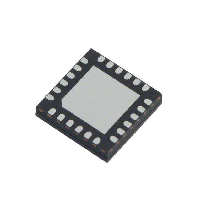
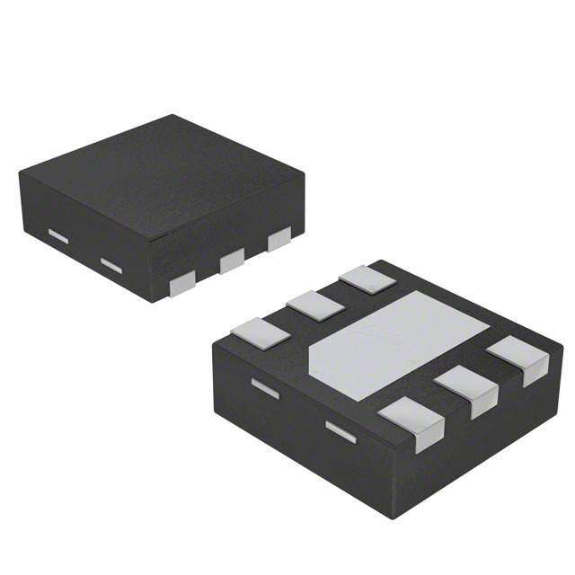
| 产品图片 |
|
| rohs | 符合RoHS无铅 / 符合限制有害物质指令(RoHS)规范要求 |
| 产品系列 | 开关 IC,电源开关 IC - 配电,Fairchild Semiconductor FPF2195- |
| 数据手册 | |
| 产品型号 | FPF2195 |
| Rds(On) | 80 毫欧 |
| 产品目录页面 | |
| 产品种类 | 电源开关 IC - 配电 |
| 供应商器件封装 | 6-WLCSP |
| 其它名称 | FPF2195DKR |
| 内部开关 | 是 |
| 包装 | Digi-Reel® |
| 单位重量 | 60 mg |
| 商标 | Fairchild Semiconductor |
| 安装类型 | 表面贴装 |
| 安装风格 | SMD/SMT |
| 导通电阻—最大值 | 135 mOhms |
| 封装 | Reel |
| 封装/外壳 | 6-UFBGA,WLCSP |
| 封装/箱体 | WLCSP-8 |
| 工作温度 | -40°C ~ 85°C |
| 工作电源电压 | 1.8 V to 5.5 V |
| 工厂包装数量 | 3000 |
| 最大功率耗散 | 1.2 W |
| 最大工作温度 | + 85 C |
| 最大输入电压 | 5.5 V |
| 最小工作温度 | - 40 C |
| 最小输入电压 | 1.8 V |
| 标准包装 | 1 |
| 电压-输入 | 1.8 V ~ 5.5 V |
| 电流限制 | 可调 |
| 空闲时间—最大值 | 125 us |
| 类型 | 高端开关 |
| 系列 | FPF2195 |
| 输出数 | 1 |
| 运行时间—最大值 | 40 us |


- 商务部:美国ITC正式对集成电路等产品启动337调查
- 曝三星4nm工艺存在良率问题 高通将骁龙8 Gen1或转产台积电
- 太阳诱电将投资9.5亿元在常州建新厂生产MLCC 预计2023年完工
- 英特尔发布欧洲新工厂建设计划 深化IDM 2.0 战略
- 台积电先进制程称霸业界 有大客户加持明年业绩稳了
- 达到5530亿美元!SIA预计今年全球半导体销售额将创下新高
- 英特尔拟将自动驾驶子公司Mobileye上市 估值或超500亿美元
- 三星加码芯片和SET,合并消费电子和移动部门,撤换高东真等 CEO
- 三星电子宣布重大人事变动 还合并消费电子和移动部门
- 海关总署:前11个月进口集成电路产品价值2.52万亿元 增长14.8%


PDF Datasheet 数据手册内容提取
Is Now Part of To learn more about ON Semiconductor, please visit our website at www.onsemi.com Please note: As part of the Fairchild Semiconductor integration, some of the Fairchild orderable part numbers will need to change in order to meet ON Semiconductor’s system requirements. Since the ON Semiconductor product management systems do not have the ability to manage part nomenclature that utilizes an underscore (_), the underscore (_) in the Fairchild part numbers will be changed to a dash (-). This document may contain device numbers with an underscore (_). Please check the ON Semiconductor website to verify the updated device numbers. The most current and up-to-date ordering information can be found at www.onsemi.com. Please email any questions regarding the system integration to Fairchild_questions@onsemi.com. ON Semiconductor and the ON Semiconductor logo are trademarks of Semiconductor Components Industries, LLC dba ON Semiconductor or its subsidiaries in the United States and/or other countries. ON Semiconductor owns the rights to a number of patents, trademarks, copyrights, trade secrets, and other intellectual property. A listing of ON Semiconductor’s product/patent coverage may be accessed at www.onsemi.com/site/pdf/Patent-Marking.pdf. ON Semiconductor reserves the right to make changes without further notice to any products herein. ON Semiconductor makes no warranty, representation or guarantee regarding the suitability of its products for any particular purpose, nor does ON Semiconductor assume any liability arising out of the application or use of any product or circuit, and specifically disclaims any and all liability, including without limitation special, consequential or incidental damages. Buyer is responsible for its products and applications using ON Semiconductor products, including compliance with all laws, regulations and safety requirements or standards, regardless of any support or applications information provided by ON Semiconductor. “Typical” parameters which may be provided in ON Semiconductor data sheets and/or specifications can and do vary in different applications and actual performance may vary over time. All operating parameters, including “Typicals” must be validated for each customer application by customer’s technical experts. ON Semiconductor does not convey any license under its patent rights nor the rights of others. ON Semiconductor products are not designed, intended, or authorized for use as a critical component in life support systems or any FDA Class 3 medical devices or medical devices with a same or similar classification in a foreign jurisdiction or any devices intended for implantation in the human body. Should Buyer purchase or use ON Semiconductor products for any such unintended or unauthorized application, Buyer shall indemnify and hold ON Semiconductor and its officers, employees, subsidiaries, affiliates, and distributors harmless against all claims, costs, damages, and expenses, and reasonable attorney fees arising out of, directly or indirectly, any claim of personal injury or death associated with such unintended or unauthorized use, even if such claim alleges that ON Semiconductor was negligent regarding the design or manufacture of the part. ON Semiconductor is an Equal Opportunity/Affirmative Action Employer. This literature is subject to all applicable copyright laws and is not for resale in any manner.
F P F 2 1 September 2014 9 3 / F P F 2 1 9 FPF2193 / FPF2194 / FPF2195 4 / Full-Function Load Switch with Adjustable Current Limit F P F 2 1 9 5 Features Description — <1.8 to 5.5 V Input Voltage Range The FPF2193, FPF2194, and FPF2195 form a series of F u Controlled Turn-On load switches that provides full protection to systems ll and loads that may encounter large current conditions. F 0.1 to 1.5 A Adjustable Current Limit These devices contain a 55 mΩ current-limited P- u n Under-Voltage Lockout channel MOSFET that can operate over an input c voltage range of 1.8 to 5.5 V. Internally, current is t i Thermal Shutdown prevented from flowing when the MOSFET is off and the o n <2 µA Shutdown Current output voltage is higher than the input voltage. Switch L control is by a logic input (ON) capable of interfacing o Auto Restart directly with low-voltage control signals. Each part a d Fast Current Limit Response Time contains thermal shutdown protection that shuts off the S switch to prevent damage to the part when a continuous w 5 µs to Moderate Over Currents over-current condition causes excessive heating. i t c 30 ns to Hard Shorts When the switch current reaches the current limit, the h parts operate in a constant-current mode to prohibit w Fault Blanking excessive currents from causing damage. For the it Reverse Current Blocking FPF2193 and FPF2194, if the constant current condition h A still persists after 30 ms, the parts shut off the switch d Applications and pull the fault signal pin (FLAGB) LOW. The ju FPF2193 has an auto-restart feature that turns the s PDAs switch on again after 450 ms if the ON pin is still active. ta The FPF2194 does not have this auto-restart feature, so b Cell Phones the switch remains off until the ON pin is cycled. The le Handheld GPS Devices FPF2195 does not turn off after a current limit fault, but Cu remains in the constant-current mode indefinitely. The Portable Enterprise / Industrial Devices minimum current limit can be set as low as 45 mA. rre Digital Cameras These parts are available in a space-saving six ball nt Peripheral Ports and Accessories advanced 0.98 x 1.48 mm WLCSP package. Li m Portable Medical Equipment it Hot Swap Supplies Ordering Information Current Current Limit Blanking Auto-Restart ON Pin Part Number Top Mark Limit [mA] Time [ms] Time [ms] Activity FPF2193 15/30/60 225/450/900 S6 FPF2194 100-1500 15/30/60 NA S7 Active HIGH FPF2195 0 NA S9 FPF2195BUCX 45-1500 0 NA SY © 2009 Fairchild Semiconductor Corporation www.fairchildsemi.com FPF2193/4/5 • Rev. 1.0.9
F P Application Diagram F 2 1 9 3 / F P F 2 1 9 4 / F P F 2 1 9 5 — F u l Figure 1. Typical Application l F u n c t i o n Block Diagram L o a d S w i t c h w i t h A d j u s t a b l e C u r r e n t L i m i t Figure 2. Functional Block Diagram © 2009 Fairchild Semiconductor Corporation www.fairchildsemi.com FPF2193/4/5 • Rev. 1.0.9 2
F P F Pin Configuration 2 1 9 3 / F P F 2 1 9 4 / F P F 2 1 9 5 — F u Figure 3. 1.0 x 1.5 mm Chip-Scale Package l l F u n c t i o n L o a d S w i t c h w i t h A d j u s t a Figure 4. Pin Configuration (Bottom View) b l e C u r Pin Definitions r e n t Pin # Name Description L i C1 ISET Current Limit Set Input. A resistor from ISET to ground sets the current limit for the switch. m i B2 VIN Supply Input. Input to the power switch and the supply voltage for the IC. t B1 V Switch Output. Output of the power switch. OUT Fault Output. Active LOW, open-drain output that indicates an over-current supply, under- A1 FLAGB voltage, or over-temperature state. C2 GND Ground. A2 ON ON control input, active HIGH. © 2009 Fairchild Semiconductor Corporation www.fairchildsemi.com FPF2193/4/5 • Rev. 1.0.9 3
F P Absolute Maximum Ratings F 2 Stresses exceeding the absolute maximum ratings may damage the device. The device may not function or be 1 9 operable above the recommended operating conditions and stressing the parts to these levels is not recommended. 3 In addition, extended exposure to stresses above the recommended operating conditions may affect device reliability. / F The absolute maximum ratings are stress ratings only. P F Symbol Parameter Min. Max. Unit 2 1 9 VIN, VOUT, ON, FLAGB, ISET to GND -0.3 6.0 V 4 PD Power Dissipation at TA = 25°C(1) 1.2 W / F P TJ Operating Temperature Range -40 +125 °C F T Storage Temperature -65 +150 °C 2 STG 1 9 ΘJA Thermal Resistance, Junction to Ambient 85 °C/W 5 — Human Body Model, JESD22-A114 8000 ESD Electrostatic Discharge Capability V F Machine Model, JESD22-A115 400 u l Note: l F 1. Package power dissipation on one-square inch pad, two-ounce copper board. u n c t i o n Recommended Operating Conditions L o The Recommended Operating Conditions table defines the conditions for actual device operation. Recommended a d operating conditions are specified to ensure optimal performance to the datasheet specifications. Fairchild does not S recommend exceeding them or designing to Absolute Maximum Ratings. w i t Symbol Parameter Min. Max. Unit c h V Input Voltage 1.8 5.5 V w IN i t TA Ambient Operating Temperature -40 +85 °C h A d j u s t a b l e C u r r e n t L i m i t © 2009 Fairchild Semiconductor Corporation www.fairchildsemi.com FPF2193/4/5 • Rev. 1.0.9 4
F Electrical Characteristics P F V = 1.8 to 5.5 V, T = -40 to +85°C unless otherwise noted. Typical values are at V = 3.3 V and T = 25°C. 2 IN A IN A 1 9 Symbol Parameter Conditions Min. Typ. Max. Units 3 Basic Operation / F V Operating Voltage 1.8 5.5 V P IN F VIN=1.8 V 70 2 1 IQ Quiescent Current IOUT=0 mA, VON=VIN VIN=3.3 V 75 µA 9 4 VIN=5.5 V 80 / T =25°C, I =200 mA 55 80 F RON On Resistance A OUT mΩ P TA=-40 to 85°C, IOUT=200 mA 135 F 2 V On Input Logic High Voltage VIN=1.8 V 0.8 V 1 IH ON V =5.5 V 1.4 9 IN 5 VIN=1.8 V 0.5 — V On Input Logic Low Voltage V IL V =5.5 V 1.0 IN F I On Input Leakage V =V or GND -1 0 1 µA u IN ON IN l l V V Shutdown Current VON=0 V, VIN=5.5 V, -2 2 µA F IN_SD IN V =Short to GND u OUT n FLAGB Output Logic Low VIN=5 V, ISINK=10 mA 0.05 0.20 c VFLB_L Voltage VIN=1.8 V, ISINK=10 mA 0.12 0.30 V tio n FLAGB Output Logic High IFLB_H Leakage Current VIN=5 V, Switch ON 1 µA L o Reverse Block a d V =0 V, V =5.5 V, I V Shutdown Current ON OUT -2 2 µA S SDT OUT VIN=Short-to-GND w Vbreakdown Reverse Breakdown Voltage VIN=VON=0 V, IOUT=200 µA 9 V itc Protections h Current Limit V =3.3 V, V =3.0 V, R =690 Ω 600 800 1000 mA w IN OUT SET i ILIM CFPurFr2e1n9t 5LBimUitC fXor VRIN=4=.155 V.8, VKOΩU T =4.2 V, 35 45 60 mA th A SET d ILIM(MIN) Minimum Current Limit VRISNE=T3=.535 V1,6 V ΩO UT=3.0 V, 100 ma jus t Shutdown Threshold 140 a b TSD Thermal Shutdown Return from Shutdown 130 °C le Hysteresis 10 C V Under-Voltage Lockout V Increasing 1.55 1.65 1.75 V u UVLO IN r r Under-Voltage Lockout e V 50 mV UVLO_HYST Hysteresis n t Dynamic L i td Delay On Time R =500 Ω, C =0.1 µF 20 µs m ON L L i tR VOUT Rise Time RL=500 Ω, CL=0.1 µF 20 µs t tON Turn-On Time RL=500 Ω, CL=0.1 µF 40 µs td Delay Off Time R =500 Ω, C =0.1 µF 15 µs OFF L L tF VOUT Fall Time RL=500 Ω, CL=0.1 µF 110 µs t Turn-Off Time R =500 Ω, C =0.1 µF 125 µs OFF L L t Over-Current Blanking Time FPF2193, FPF2194 15 30 60 ms BLANK t Auto-Restart FPF2193 Only 225 450 900 ms RSTRT V =V =3.3 V, Moderate Over- IN OUT 5 µs t Short-Circuit Response Time Current Condition SC V =V =3.3 V, Hard Short 30 ns IN OUT © 2009 Fairchild Semiconductor Corporation www.fairchildsemi.com FPF2193/4/5 • Rev. 1.0.9 5
F P Typical Performance Characteristics F 2 1 9 3 / F P F 2 1 9 4 / F P F 2 1 9 5 — F u l l F Figure 5. Quiescent Current vs. Input Voltage Figure 6. Quiescent Current vs. Input Voltage u n c t i o n L o a d S w i t c h w i t h A d j u s t a b Figure 7. Quiescent Current vs. Temperature Figure 8. VONHigh Voltage vs. Input Voltage le C u r r e n t L i m i t Figure 9. V Low Voltage vs. Input Voltage Figure 10. Current Limit vs. Output Voltage ON © 2009 Fairchild Semiconductor Corporation www.fairchildsemi.com FPF2193/4/5 • Rev. 1.0.9 6
F Typical Performance Characteristics (Continued) P F 2 1 9 3 / F P F 2 1 9 4 / F P F 2 1 9 5 — F u l l Figure 11. Current Limit vs. Temperature Figure 12. R vs. V F ON IN u n c t i o n L o a d S w i t c h w i t h A d j u s t a b Figure 13. RON vs. Temperature Figure 14. tON/ tOFF vs. Temperature le C u r r e n t L i m i t Figure 15. t / t vs. Temperature Figure 16. t vs. Temperature RISE FALL RSTRT © 2009 Fairchild Semiconductor Corporation www.fairchildsemi.com FPF2193/4/5 • Rev. 1.0.9 7
F Typical Performance Characteristics (Continued) P F 2 1 9 3 / F P F 2 1 9 4 / F P F 2 1 9 5 — F u l l Figure 17. t vs.Temperature Figure 18. t Response F BLANK ON u n c t i o n L o a d S w i t c h w i t h A d j u s t a b Figure 19. t Response Figure 20. Short-Circuit Response Time l OFF e (Output Shorted to GND) C u r r e n t L i m i t Figure 21. Current Limit Response Time Figure 22. Current Limit Response Time (Switch is Powered into a Short) (Output is Loaded by 2.2 Ω, C =0.1 µF) OUT © 2009 Fairchild Semiconductor Corporation www.fairchildsemi.com FPF2193/4/5 • Rev. 1.0.9 8
F P Typical Performance Characteristics (Continued) F 2 1 9 3 / F P F 2 1 9 4 / F P F 2 1 9 5 — F u l l F Figure 23. Current Limit Response Time Figure 24. Short-Circuit Detection Function(2) u (Output is Loaded by 2.2 Ω, C =10 µF) n OUT c t i o n L o a d S w i t c h w i t h A d j u s t a b l e Figure 25. t vs. Response(3) Figure 26. t vs. Response(3) C BLANK RESTART u Notes: rr e 2. When the output voltage is below VSCTH=1.1 V, the current limit value is set at 62.5% of the current limit value. n 3. V signal forces the device to go into over-current condition by loading. t DRV L i m i t © 2009 Fairchild Semiconductor Corporation www.fairchildsemi.com FPF2193/4/5 • Rev. 1.0.9 9
Functional Description F P The FPF2193, FPF2194, and FPF2195 are current- heavy load. When the output voltage drops below V , F SCTH 2 limited switches that protect systems and loads that can the short-circuit detection threshold voltage, the current 1 be damaged or disrupted by the application of high limit value is re-conditioned and the short-circuit current- 9 3 currents. The core of each device is a 55 mΩ P-channel limit value is decreased to 62.5% of the current limit / MOSFET and a controller capable of functioning over the value. This keeps the power dissipation of the part below F wide input operating range of 1.8- 5.5 V. The controller a certain limit even at dead-short conditions at 5.5 V input P F protects against system malfunctions through current voltage. The VSCTH value is set to be 1 V. At around 1.1 V 2 limiting, under-voltage lockout, and thermal shutdown. of output voltage, the switch is removed from short-circuit 1 9 The current limit is adjustable from 100 mA (45 mA for current-limiting mode and the current limit is set to the 4 FPF2195BUCX) to 1.5 A through the selection of an current limit value. / external resistor. F Under-Voltage Lockout (UVLO) P On/Off Control F The under-voltage lockout turns the switch off if the input 2 The ON pin controls the state of the switch. When ON is voltage drops below the under-voltage lockout threshold. 1 9 HIGH, the switch is in ON state. Activating ON With the ON pin active, the input voltage rising above the 5 continuously holds the switch in the ON state so long as under-voltage lockout threshold causes a controlled turn- — there is no fault. For all versions, an under-voltage on VIN on of the switch, which limits current over shoot. F or a junction temperature in excess of 140°C overrides Thermal Shutdown u the ON control to turn off the switch. In addition, l l excessive currents cause the switch to turn off in the The thermal shutdown protects the die from internally or F FPF2193 and FPF2194. The FPF2193 has an auto- externally generated excessive temperatures. During an u restart feature that automatically turns the switch on again over-temperature condition, FLAGB is activated and the nc after 450 ms. For the FPF2194, the ON pin must be switch is turned off. The switch automatically turns on ti again if temperature of the die drops below the o toggled to turn the switch on again. The FPF2195 does n not turn off in response to an over-current condition, but threshold temperature. L remains operating in constant-current mode as long as Reverse-Current Blocking o a ON is active and the thermal shutdown or under-voltage The entire FPF2193/94/95 family has a reverse current d lockout have not activated. blocking feature that protects the input source against S Fault Reporting current flow from output to input. For a standard USB w i power design, this is an important feature to protect the t Upon the detection of an over-current, input under- c voltage, or over-temperature condition, FLAGB signals USB host from being damaged due to reverse current h the fault mode by activating LOW. For the FPF2193 and flow on VBUS. w i FPF2194, the FLAGB goes LOW at the end of the When the load switch is OFF, no current flows from the t h blanking time, while FLAGB goes LOW immediately for output to the input. If the switch is turned on and the A the FPF2195. FLAGB remains LOW through the auto- output voltage is greater than input voltage, this feature is d restart time for the FPF2195. For the FPF2194, FLAGB is activated and turns off the switch. This prevents any ju latched LOW and ON must be toggled to release it. With current flow from output to input. The reverse-current s t the FPF2195, FLAGB is LOW during the faults and blocking feature is deactivated if the V - V is smaller a OUT IN b immediately returns HIGH at the end of the fault than a typically 50 mV threshold. During this time, some l e condition. FLAGB is an open-drain MOSFET that requires current (50 mV/RON) flows from the output to input until C a pull-up resistor between V and FLAGB. During input voltage becomes greater than output voltage. IN u shutdown, the pull-down on FLAGB is disabled to reduce FLAGB operation is independent of the reverse-current r r current draw from the supply. blocking and does not report a fault condition if this e n feature is activated. Current Limiting t L The current limit ensures that the current through the i m switch doesn't exceed a maximum value, while not i limiting at less than a minimum value. The current at t which the parts limit is adjustable through the selection of an external resistor connected to I . Information for SET selecting the resistor is found in the Application Information section. The FPF2193 and FPF2194 have a blanking time of 30 ms, nominally, during which the switch acts as a constant current source. At the end of the blanking time, the switch is turned off. The FPF2195 Figure 27. Timing Diagram has no current limit blanking period, so it remains in a where: constant current state until the ON pin is deactivated or td = Delay On Time the thermal shutdown turns off the switch. ON t = V Rise Time R OUT For preventing the switch from large power dissipation t = Turn-On Time ON during heavy load, a short-circuit detection feature is td = Delay Off Time OFF introduced. Short-circuit condition is detected by, t = V Fall Time F OUT observing the output voltage. The switch is put into short- t = Turn-Off Time OFF circuit current-limiting mode if the switch is loaded with a © 2009 Fairchild Semiconductor Corporation www.fairchildsemi.com FPF2193/4/5 • Rev. 1.0.9 10
F P Application Information F 2 1 9 3 / F P F 2 1 9 4 / F P F 2 1 9 5 — Figure 28. Typical Application Setting Current Limit F Input Capacitor u l The FPF2193, FPF2194, and FPF2195 current limit is To limit the voltage drop on the input supply caused by l F set with an external resistor connected between ISET and transient inrush currents when the switch is turned on u GND. This resistor is selected using the following into a discharged load capacitor or a short-circuit, a n equation: capacitor needs to be placed between VIN and GND. A ct i 551.6 0.1 µF ceramic capacitor, CIN, placed close to the pins is o RSET = ILIM (1) ufusruthaellry resudfuficceie tnhte. vHoiglthaegre vdarolupe. s of CIN can be used to n Lo R is in Ω and I is in Amps. a SET SET Output Capacitor d Table 1 can also be used to select RSET. A typical A 0.1 µF capacitor, COUT, should be placed between Sw application would be the 500 mA current required by a V and GND. This capacitor prevents parasitic board OUT i single USB port. Using Table 1, an appropriate selection inductances from forcing VOUT below GND when the tc for the RSET resistor would be 788 Ω. This ensures that switch turns off. For the FPF2193 and FPF2194, the h the port load could draw 525 mA, but not more than total output capacitance needs to be kept below a w 875 mA. Likewise for a dual-port system; an RSET of maximum value, COUT(max), to prevent the part from ith 368 Ω always delivers at least 1125 mA and never more registering an over-current condition and turning off the A than 1875 mA. switch. The maximum output capacitance can be d Table 1. Current Limit Various RSET Values determined from the following formula: ju s RSET(Ω) MLiinm. iCt u(mrrAen) t TLyipm. iCt u(mrrAen) t MLaixm. iCt u(mrrAen) t COUT(max)=ILIM(max)×tBLANK(min) (2) tab V l 368 1125 1500 1875 IN e C 441 928 1250 1562 Power Dissipation u r 552 750 1000 1250 During normal operation as a switch, the power r e 613 675 900 1125 dissipated depends upon the level at which the current n t limit is set. The maximum allowed setting for the current 690 600 800 1000 L limit is 1.5 A and results in a power dissipation of: i m 788 525 700 875 919 450 600 750 P=(ILIM)2×RON =(1.5)2×0.055=123.75mW (3) it If the part goes into current limit, the maximum power 1103 375 500 625 dissipation occurs when the output is shorted to ground. 1226 338 450 563 For the FPF2193, the power dissipation scales by the auto-restart time, t , and the over-current blanking 1379 300 400 500 RSTRT time, t , so that the maximum power dissipated is: BLANK 1576 263 350 438 1839 225 300 375 P(max)= tBLANK ×V (max)×I (max) 2206 188 250 313 t +t IN LIM BLANK RSTRT (4) 2758 150 200 250 30 = ×5.5×1.5=515.6mW 3677 113 150 188 30+450 5516 75 100 125 15800(4) 35 45 60 Note: 4. FPF2195BUCX only. © 2009 Fairchild Semiconductor Corporation www.fairchildsemi.com FPF2193/4/5 • Rev. 1.0.9 11
F P This is more power than the package can dissipate, but Board Layout F 2 the thermal shutdown of the part activates to protect the 1 part from damage due to excessive heating. When For best performance, all traces should be as short as 9 possible. To be most effective, the input and output 3 using the FPF2194, attention must be given to the capacitors should be placed close to the device to / manual resetting of the part. The junction temperature is F minimize the effects that parasitic trace inductances P only able to increase to the thermal shutdown threshold. may have on normal and short-circuit operation. Using F Once this temperature has been reached, toggling ON 2 wide traces for V , V , and GND help to minimize does not turn the switch on until the junction IN OUT 1 parasitic electrical effects along with minimizing the 9 temperature drops. For the FPF2195, a short on the 4 output causes the part to operate in a constant-current case-to-ambient thermal impedance. / state, dissipating a worst-case power of: F P F P(max)=V (max)×I (max) 2 IN LIM (5) 1 =5.5×1.5=8.25W 9 5 This large amount of power activates the thermal — shutdown and the part cycles in and out of thermal F shutdown as long as the ON pin is active and the short u l is present. l F u n c t i o n L o a d S w i t c h w i t h A d j u s t a b l e C u r r e n t L i m i t © 2009 Fairchild Semiconductor Corporation www.fairchildsemi.com FPF2193/4/5 • Rev. 1.0.9 12
F P Physical Dimensions F 2 1 9 3 0.03 C E A F (Ø0.250) / 2X F Cu Pad P B (Ø0.350) SOLDER MASK A1 F 2 OPENING 1 BALL A1 (1.00) 94 INDEX AREA D / F (0.50) P 0.03 C F 2X 2 1 TOP VIEW RECOMMENDED LAND PATTERN 95 (NSMD PAD TYPE) — F 0.06 C u l 0.625 0.332±0.018 l 0.05 C 0.539 E 0.250±0.025 F u n c t i C SEATING PLANE D o n SIDE VIEWS L o a d NOTES: S w A. NO JEDEC REGISTRATION APPLIES. i t c 0.005 C A B B. DIMENSIONS ARE IN MILLIMETERS. h w Ø0.315 +/- .025 C. DIMENSIONS AND TOLERANCE i 6X t 0.50 PER ASMEY14.5M, 1994. h A C D. DATUM C IS DEFINED BY THE SPHERICAL d 1.00 B (Y) ±0.018 CROWNS OF THE BALLS. ju 0.50 s A E. PACKAGE NOMINAL HEIGHT IS 582 MICRONS t a ±43 MICRONS (539-625 MICRONS). b 1 2 F l e (X) ±0.018 F. FOR DIMENSIONS D, E, X, AND Y SEE C PRODUCT DATASHEET. u BOTTOM VIEW G. DRAWING FILNAME: MKT-UC006AFrev2. rr e n t L i m Figure 29. 6-Ball, Wafer-Level Chip-Scale Package (WLCSP) i t D E X Y 1.480±0.030 0.980±0.030 0.240 0.240 © 2009 Fairchild Semiconductor Corporation www.fairchildsemi.com FPF2193/4/5 • Rev. 1.0.9 13
F P F 2 1 9 3 / F P F 2 1 9 4 / F P F 2 1 9 5 — F u l l F u n c t i o n L o a d S w i t c h w i t h A d j u s t a b l e C u r r e n t L i m i t © 2009 Fairchild Semiconductor Corporation www.fairchildsemi.com FPF2193/4/5 • Rev. 1.0.9 14
ON Semiconductor and are trademarks of Semiconductor Components Industries, LLC dba ON Semiconductor or its subsidiaries in the United States and/or other countries. ON Semiconductor owns the rights to a number of patents, trademarks, copyrights, trade secrets, and other intellectual property. A listing of ON Semiconductor’s product/patent coverage may be accessed at www.onsemi.com/site/pdf/Patent−Marking.pdf. ON Semiconductor reserves the right to make changes without further notice to any products herein. ON Semiconductor makes no warranty, representation or guarantee regarding the suitability of its products for any particular purpose, nor does ON Semiconductor assume any liability arising out of the application or use of any product or circuit, and specifically disclaims any and all liability, including without limitation special, consequential or incidental damages. Buyer is responsible for its products and applications using ON Semiconductor products, including compliance with all laws, regulations and safety requirements or standards, regardless of any support or applications information provided by ON Semiconductor. “Typical” parameters which may be provided in ON Semiconductor data sheets and/or specifications can and do vary in different applications and actual performance may vary over time. All operating parameters, including “Typicals” must be validated for each customer application by customer’s technical experts. ON Semiconductor does not convey any license under its patent rights nor the rights of others. ON Semiconductor products are not designed, intended, or authorized for use as a critical component in life support systems or any FDA Class 3 medical devices or medical devices with a same or similar classification in a foreign jurisdiction or any devices intended for implantation in the human body. Should Buyer purchase or use ON Semiconductor products for any such unintended or unauthorized application, Buyer shall indemnify and hold ON Semiconductor and its officers, employees, subsidiaries, affiliates, and distributors harmless against all claims, costs, damages, and expenses, and reasonable attorney fees arising out of, directly or indirectly, any claim of personal injury or death associated with such unintended or unauthorized use, even if such claim alleges that ON Semiconductor was negligent regarding the design or manufacture of the part. ON Semiconductor is an Equal Opportunity/Affirmative Action Employer. This literature is subject to all applicable copyright laws and is not for resale in any manner. PUBLICATION ORDERING INFORMATION LITERATURE FULFILLMENT: N. American Technical Support: 800−282−9855 Toll Free ON Semiconductor Website: www.onsemi.com Literature Distribution Center for ON Semiconductor USA/Canada 19521 E. 32nd Pkwy, Aurora, Colorado 80011 USA Europe, Middle East and Africa Technical Support: Order Literature: http://www.onsemi.com/orderlit Phone: 303−675−2175 or 800−344−3860 Toll Free USA/Canada Phone: 421 33 790 2910 Fax: 303−675−2176 or 800−344−3867 Toll Free USA/Canada Japan Customer Focus Center For additional information, please contact your local Email: orderlit@onsemi.com Phone: 81−3−5817−1050 Sales Representative © Semiconductor Components Industries, LLC www.onsemi.com www.onsemi.com 1
Mouser Electronics Authorized Distributor Click to View Pricing, Inventory, Delivery & Lifecycle Information: O N Semiconductor: FPF2195 FPF2195BUCX