ICGOO在线商城 > 集成电路(IC) > PMIC - 配电开关,负载驱动器 > FPF1504LUCX
 Datasheet下载
- 型号: FPF1504LUCX
- 制造商: Fairchild Semiconductor
- 库位|库存: xxxx|xxxx
- 要求:
| 数量阶梯 | 香港交货 | 国内含税 |
| +xxxx | $xxxx | ¥xxxx |
查看当月历史价格
查看今年历史价格
FPF1504LUCX产品简介:
ICGOO电子元器件商城为您提供FPF1504LUCX由Fairchild Semiconductor设计生产,在icgoo商城现货销售,并且可以通过原厂、代理商等渠道进行代购。 FPF1504LUCX价格参考¥1.25-¥3.79。Fairchild SemiconductorFPF1504LUCX封装/规格:PMIC - 配电开关,负载驱动器, 。您可以下载FPF1504LUCX参考资料、Datasheet数据手册功能说明书,资料中有FPF1504LUCX 详细功能的应用电路图电压和使用方法及教程。
FPF1504LUCX 是安森美半导体(ON Semiconductor)生产的一款电源管理IC,属于配电开关和负载驱动器类别。该器件是一款单通道负载开关,集成了一个低导通电阻的N沟道MOSFET,适用于需要高效电源管理的便携式和低功耗应用。

其主要功能包括过流保护、欠压锁定(UVLO)、自动放电控制等,具有较高的可靠性和集成度。典型应用场景包括:

1. 移动设备:如智能手机、平板电脑和笔记本电脑中的外设电源管理,用于控制如摄像头模块、显示屏、无线模块等负载的供电。
2. 工业控制系统:用于工业自动化设备中的传感器、执行器或通信模块的电源切换与保护。
3. 消费电子产品:例如数字相机、便携式游戏机等,用于实现负载的软启动和电源隔离。
4. 通信设备:在网络设备或通信模块中用于电源分配管理和负载隔离,提升系统稳定性和安全性。

该器件采用小型封装(如UCSP),适合空间受限的设计,是实现高效、可靠电源管理的理想选择。
| 参数 | 数值 |
| 产品目录 | 集成电路 (IC)半导体 |
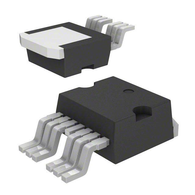
| 描述 | IC LOAD MGMT SWITCH ADV 4WLCSP电源开关 IC - 配电 Advanced Load Management Switch |
| 产品分类 | PMIC - 电源分配开关集成电路 - IC |
| 品牌 | Fairchild Semiconductor |
| 产品手册 | |
| 产品图片 | |
| 产品系列 | 开关 IC,电源开关 IC - 配电,Fairchild Semiconductor FPF1504LUCXIntelliMax™ |
| 数据手册 | |
| 产品型号 | FPF1504LUCX |
| Rds(On) | 15 毫欧 |
| rohs | 无铅 / 符合限制有害物质指令(RoHS)规范要求 |
| 产品 | Load Switches |
| 产品种类 | 电源开关 IC - 配电 |
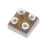
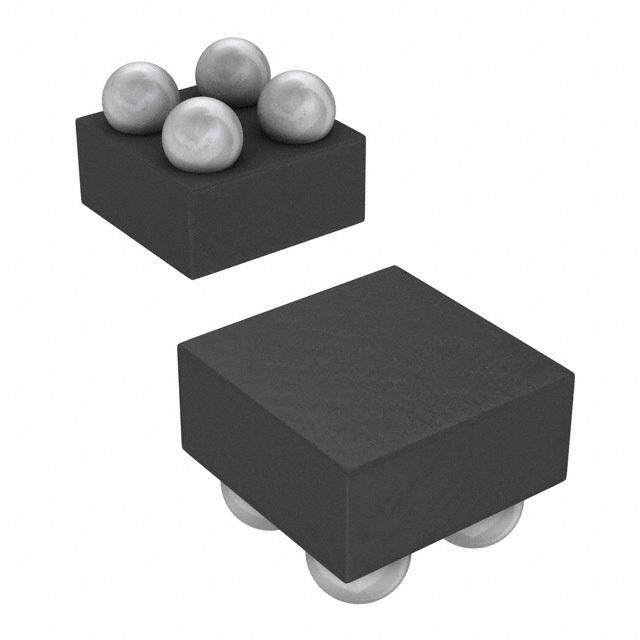
| 供应商器件封装 | 4-WLCSP(0.96x0.96) |
| 其它名称 | FPF1504LUCXDKR |
| 内部开关 | 是 |
| 包装 | Digi-Reel® |
| 单位重量 | 42 mg |
| 商标 | Fairchild Semiconductor |
| 安装类型 | 表面贴装 |
| 安装风格 | SMD/SMT |
| 导通电阻—最大值 | 30 mOhms |
| 封装 | Reel |
| 封装/外壳 | 4-UFBGA,WLCSP |
| 封装/箱体 | WLCSP-4 |
| 工作温度 | -40°C ~ 85°C |
| 工作电源电压 | 1 V to 3.6 V |
| 工厂包装数量 | 3000 |
| 开关电流—最大值 | 1.5 A |
| 最大功率耗散 | 1 W |
| 最大工作温度 | + 85 C |
| 最小工作温度 | - 40 C |
| 标准包装 | 1 |
| 电压-输入 | 1 V ~ 3.6 V |
| 电流限制 | 1.5A |
| 空闲时间—最大值 | 16 us |
| 类型 | 高端开关 |
| 系列 | FPF1504 |
| 输出数 | 1 |
| 输出端数量 | 1 Output |
| 运行时间—最大值 | 210 us |


- 商务部:美国ITC正式对集成电路等产品启动337调查
- 曝三星4nm工艺存在良率问题 高通将骁龙8 Gen1或转产台积电
- 太阳诱电将投资9.5亿元在常州建新厂生产MLCC 预计2023年完工
- 英特尔发布欧洲新工厂建设计划 深化IDM 2.0 战略
- 台积电先进制程称霸业界 有大客户加持明年业绩稳了
- 达到5530亿美元!SIA预计今年全球半导体销售额将创下新高
- 英特尔拟将自动驾驶子公司Mobileye上市 估值或超500亿美元
- 三星加码芯片和SET,合并消费电子和移动部门,撤换高东真等 CEO
- 三星电子宣布重大人事变动 还合并消费电子和移动部门
- 海关总署:前11个月进口集成电路产品价值2.52万亿元 增长14.8%


PDF Datasheet 数据手册内容提取
Is Now Part of To learn more about ON Semiconductor, please visit our website at www.onsemi.com Please note: As part of the Fairchild Semiconductor integration, some of the Fairchild orderable part numbers will need to change in order to meet ON Semiconductor’s system requirements. Since the ON Semiconductor product management systems do not have the ability to manage part nomenclature that utilizes an underscore (_), the underscore (_) in the Fairchild part numbers will be changed to a dash (-). This document may contain device numbers with an underscore (_). Please check the ON Semiconductor website to verify the updated device numbers. The most current and up-to-date ordering information can be found at www.onsemi.com. Please email any questions regarding the system integration to Fairchild_questions@onsemi.com. ON Semiconductor and the ON Semiconductor logo are trademarks of Semiconductor Components Industries, LLC dba ON Semiconductor or its subsidiaries in the United States and/or other countries. ON Semiconductor owns the rights to a number of patents, trademarks, copyrights, trade secrets, and other intellectual property. A listing of ON Semiconductor’s product/patent coverage may be accessed at www.onsemi.com/site/pdf/Patent-Marking.pdf. ON Semiconductor reserves the right to make changes without further notice to any products herein. ON Semiconductor makes no warranty, representation or guarantee regarding the suitability of its products for any particular purpose, nor does ON Semiconductor assume any liability arising out of the application or use of any product or circuit, and specifically disclaims any and all liability, including without limitation special, consequential or incidental damages. Buyer is responsible for its products and applications using ON Semiconductor products, including compliance with all laws, regulations and safety requirements or standards, regardless of any support or applications information provided by ON Semiconductor. “Typical” parameters which may be provided in ON Semiconductor data sheets and/or specifications can and do vary in different applications and actual performance may vary over time. All operating parameters, including “Typicals” must be validated for each customer application by customer’s technical experts. ON Semiconductor does not convey any license under its patent rights nor the rights of others. ON Semiconductor products are not designed, intended, or authorized for use as a critical component in life support systems or any FDA Class 3 medical devices or medical devices with a same or similar classification in a foreign jurisdiction or any devices intended for implantation in the human body. Should Buyer purchase or use ON Semiconductor products for any such unintended or unauthorized application, Buyer shall indemnify and hold ON Semiconductor and its officers, employees, subsidiaries, affiliates, and distributors harmless against all claims, costs, damages, and expenses, and reasonable attorney fees arising out of, directly or indirectly, any claim of personal injury or death associated with such unintended or unauthorized use, even if such claim alleges that ON Semiconductor was negligent regarding the design or manufacture of the part. ON Semiconductor is an Equal Opportunity/Affirmative Action Employer. This literature is subject to all applicable copyright laws and is not for resale in any manner.
F P F 1 5 September 2016 0 4 / F P F FPF1504 / FPF1504L 1 5 0 Advanced Load Management Switch 4 L — Features Description A d v 1.0 V to 3.6 V Input Voltage Operating Range The FPF1504/FPF1504L are low-RDS P-channel a n MOSFET load switches of the IntelliMAX™ family. Typical R : c DS(ON) Integrated slew-rate control prevents excessive inrush e - 15 mΩ at V =3.3 V d IN current from the supply rails with capacitive loads L - 20 mΩ at VIN=1.8 V common in power applications. In addition, the o a - 40 mΩ at VIN=1.0 V FPF1504/FPF1504L feature output discharge capability. d Slew Rate Control The input voltage range operates from 1.0 V to 3.6 V to M a Output Discharge Function fulfill today's mobile device supply requirements. Switch n a Low <1 µA Quiescent Current at VON=VIN cdoirnetcrtolyl isw bityh a lloowg-icv oinltpaugte ( OCNM pOinS) ccaopnatbrolel osfi ginntaelrsfa cainngd gem ESD Protected: 4000 V HBM, 2000 V CDM GPIOs in embedded processors. e GPIO/CMOS-Compatible Enable Circuitry nt S Active HIGH and active LOW versions w i t c Applications h Mobile Devices and Smart Phones Portable Media Devices Digital Cameras Advanced Notebook, UMPC, and MID Portable Medical Devices GPS and Navigation Equipment Figure 1. Block Diagram Ordering Information Switch Top Input Output ON Pin Part Number (Typical) Package Mark Buffer Discharge Activity At 1.8 V IN Active FPF1504UCX G4 20 mΩ CMOS YES 4-Ball, WLCSP, 0.5 mm Pitch HIGH Active 4-Ball, WLCSP with Backside FPF1504BUCX G4 20 mΩ CMOS YES HIGH Laminate, 0.5 mm Pitch Active FPF1504LUCX GZ 20 mΩ CMOS YES 4-Ball, WLCSP, 0.5 mm Pitch LOW Active 4-Ball, WLCSP with Backside FPF1504LBUCX GZ 20 mΩ CMOS YES LOW Laminate, 0.5 mm Pitch © 2012 Fairchild Semiconductor Corporation www.fairchildsemi.com FPF1504 / FPF1504L • Rev. 1.11
F P F 1 Application Diagram 5 0 4 V V T o Loa d / IN OUT F C C P IN OUT F O N 1 5 GND 0 4 L — A d Figure 2. Typical Application v a Notes: n c 1. CIN=1 F, X5R, 0603, for example Murata GRM185R60J105KE26. e d 2. C =1 F, X5R, 0805, for example Murata GRM216R61A105KA01. OUT L o a d M a n Pin Configurations a g e m e n t S w i t c h Figure 3. 1 x 1 mm WLCSP Bumps Facing Down Figure 4. 1 x 1 mm WLCSP Bumps Facing Up V A1 A2 V V A2 A1 V OUT IN IN OUT GND B1 B2 ON ON B2 B1 GND Figure 5. Pin Assignments (Top View) Figure 6. Pin Assignments (Bottom View) Pin Definitions Pin # Name Description A1 V Switch Output OUT A2 V Supply Input; Input to the Power Switch IN B1 GND Ground B2 ON ON/OFF Control © 2012 Fairchild Semiconductor Corporation www.fairchildsemi.com FPF1504 / FPF1504L • Rev. 1.11 2
F P Absolute Maximum Ratings F 1 5 Stresses exceeding the absolute maximum ratings may damage the device. The device may not function or be 0 4 operable above the recommended operating conditions and stressing the parts to these levels is not recommended. / In addition, extended exposure to stresses above the recommended operating conditions may affect device reliability. F The absolute maximum ratings are stress ratings only. P F 1 Symbol Parameter Min. Max. Unit 5 0 V V , V , V to GND -0.3 4.0 V 4 IN IN OUT ON L I Maximum Continuous Switch Current 1.5 A — SW PD Power Dissipation at TA=25°C 1.0 W A d TSTG Storage Junction Temperature -65 +150 °C v a TA Operating Temperature Range -40 +85 °C n c 1S2P with 1 Thermal Via 95 e Thermal Resistance, Junction-to-Ambient °C/W d JA 1S2P without Thermal Via 187 L o Human Body Model, a 4 JESD22-A114 d ESD Electrostatic Discharge Capability kV M Charged Device Model, 2 a JESD22-C101 n a g e m e n Recommended Operating Conditions t S The Recommended Operating Conditions table defines the conditions for actual device operation. Recommended w i operating conditions are specified to ensure optimal performance to the datasheet specifications. Fairchild does not t c recommend exceeding them or designing to Absolute Maximum Ratings. h Symbol Parameter Min. Max. Unit V Supply Voltage 1.0 3.6 V IN TA Ambient Operating Temperature -40 +85 °C © 2012 Fairchild Semiconductor Corporation www.fairchildsemi.com FPF1504 / FPF1504L • Rev. 1.11 3
F P Electrical Characteristics F 1 Unless otherwise noted, VIN=1.0 to 3.6 V, TA=-40 to +85°C; typical values are at VIN=3.3 V and TA=25°C. 50 4 Symbol Parameter Conditions Min. Typ. Max. Units / F Basic Operation P F V Supply Voltage 1.0 3.6 V 1 IN 5 0 Off Supply FPF1504 VON=GND, VOUT=Open 0.25 4 I L Q(OFF) Current FPF1504L VON= VIN, VOUT=Open 0.3 — Off Switch FPF1504 VON=GND, VOUT=GND 0.25 A ISD(OFF) Current d FPF1504L V = V , V =GND 0.3 v ON IN OUT μA a n I =0 mA, V =3.6 V, V =V 0.08 OUT IN ON IN c FPF1504 e Quiescent IOUT=0 mA, VON=VIH(MIN) 0.75 d IQ Current L IOUT=0 mA, VIN=3.6 V, VON=GND 0.08 o FPF1504L a I =0 mA, V =V 0.95 d OUT ON IL(MAX) M VIN=3.3 V, IOUT=200 mA, TA=25°C 15 30 a n V =1.8 V, I =200 mA, T =25°C 20 40 a IN OUT A g e R On Resistance V =1.5 V, I =200 mA, T =25°C 30 mΩ ON IN OUT A m V =1.0 V, I =200 mA, T =25°C 40 80 e IN OUT A n t VIN=1.8 V, IOUT=200 mA, TA=85°C(3) 35 50 S w RPD OReustpisutta Dncisec harge Pull-Down VON=0 V or VIN, IOUT=-20 mA 65 95 Ω itc h On Input Logic V FPF1504 0.8 IH High Voltage V On Input Logic V FPF1504 0.3 IL Low Voltage I On Input Leakage V =V or GND 1 μA ON ON IN Dynamic Characteristics Turn-On tDON Delay(4) FPF1504 80 V Rise R =10 Ω, C =0.1 µF, V =3.3 V, t OUT FPF1504 L L IN 130 μs R Time(4) T =25°C A t Turn-On Time(4) FPF1504 210 ON FPF1504 70 100 Turn-On tDON Delay(4) FPF1504L 95 FPF1504 110 150 V Rise R =500 Ω, C =0.1 µF, V =3.3 V, tR TiOmUeT(4) TL=25°C L IN μs FPF1504L A 115 FPF1504 180 250 t Turn-On Time(4) ON FPF1504L 210 Continued on the following page… © 2012 Fairchild Semiconductor Corporation www.fairchildsemi.com FPF1504 / FPF1504L • Rev. 1.11 4
F P Electrical Characteristics (Continued) F 1 5 Unless otherwise noted, VIN=1.0 to 3.6 V, TA=-40 to +85°C; typical values are at VIN=3.3 V and TA=25°C. 04 Symbol Parameter Conditions Min. Typ. Max. Units / F P Dynamic Characteristics (Continued) F 1 Turn-Off 5 tDOFF Delay(4) FPF1504 25 30 04 L t V Fall Time(4) FPF1504 RL=10 Ω, CL=0.1 µF, VIN=3.3 V, 2 μs — F OUT TA=25°C A d tOFF Turn-Off Time(4) FPF1504 27 va n c Turn-Off FPF1504 25 e tDOFF Delay(4) FPF1504L 2 d L o tF VOUT Fall Time(4) FFPPFF11550044L RTAL==2550°0C Ω , CL=0.1 µF, VIN=3.3 V, 1124 μs ad M FPF1504 37 a t Turn-Off Time(4) n OFF FPF1504L 16 a g Notes: e m 3. This parameter is guaranteed by design and characterization; not production tested. e 4. tDON/tDOFF/tR/tF are defined in Figure 7. n 5. Output discharge path is enabled during off. t S w i t Timing Diagram – FPF1504 c h Notes: 6. t =t + t . ON R DON 7. t =t + t . OFF F DOFF Figure 7. Timing Diagram for FPF1504 © 2012 Fairchild Semiconductor Corporation www.fairchildsemi.com FPF1504 / FPF1504L • Rev. 1.11 5
F P Typical Performance Characteristics for FPF1504 F 1 Applicable to active high version only. 5 0 4 / A) A) F NT (n NT (n PF TDOWN CURRE DOWN CURRE 1504L — U T H U S H A VIN SN d VI v a n c Figure 8. Shutdown Current vs. Temperature Figure 9. Shutdown Current vs. Supply Voltage e d L o a d M a n a g e m e n t S w i t Figure 10. Off Supply Current vs. Temperature Figure 11. Off Supply Current vs. Supply Voltage c h nt (nA) nt (nA) e e pply Curr ply Curr u p S u Q S I Q I Figure 12. Quiescent Current vs. Temperature Figure 13. Quiescent Current vs. Supply Voltage (V =V ) ON IN Figure 14. R vs. Temperature Figure 15. R vs. Supply Voltage ON ON © 2012 Fairchild Semiconductor Corporation www.fairchildsemi.com FPF1504 / FPF1504L • Rev. 1.11 6
F P Typical Performance Characteristics for FPF1504 F 1 Applicable to active high version only. 5 0 4 / F P F 1 5 0 4 L — A d v a n c Figure 16. V Rise/Fall Times vs. Temperature Figure 17. V Turn-On/Turn-Off Delays OUT OUT e (R =10 Ω) vs. Temperature (R =10 Ω) d L L L o a d M a n a g e m e n t S w i t Figure 18. V Rise/Fall Time vs. Temperature Figure 19. V Turn-On/Turn-Off Delays c OUT OUT h (RL=500 Ω) vs. Temperature (RL=500 Ω) Vin:3.3V, 1V/DIV Vin:3.3V, 1V/DIV 25C 25C Vout:3.3V, 1V/DIV Vout:3.3V, 1V/DIV IOUT:100mA/DIV IOUT:100mA/DIV ON:0-2V, 2V/DIV ON:2-0V, 2V/DIV TIME:100us/DIV TIME:10us/DIV Figure 20. Turn-On Response Figure 21. Turn-Off Response (V =3.3 V, C =0.1 µF, R =10 Ω) (V =3.3 V, C =0.1 µF, R =10 Ω) IN OUT L IN OUT L Vin:3.3V, 1V/DIV Vin:3.3V, 1V/DIV 25C 25C Vout:3.3V, 1V/DIV Vout:3.3V, 1V/DIV IOUT:10mA/DIV IOUT:10mA/DIV ON:0-2V, 2V/DIV ON:2-0V, 2V/DIV TIME:100us/DIV TIME:10us/DIV Figure 22. Turn-On Response Figure 23. Turn-Off Response (V =3.3 V, C =0.1 µF, R =500 Ω) (V =3.3 V, C =0.1 µF, R =500 Ω) IN OUT L IN OUT L © 2012 Fairchild Semiconductor Corporation www.fairchildsemi.com FPF1504 / FPF1504L • Rev. 1.11 7
F P Application Information F 1 Input Capacitor The same equation works for a device with a pull-down 5 0 IntelliMAX™ switches don’t require an input capacitor. output resistor, then RL is replaced by a parallel 4 connected pull-down and external output resistor / To reduce device inrush current, a 0.1 µF ceramic F combination, as follows: capacitor, C , is recommended close to the VIN pin. A P IN F hvoiglthaegre vdarloupe eoxfp CerINie nccaend b aes uthsee ds wtoit cfhu ritsh etur rnreeddu ocne inthtoe tF RLRPD CL2.2 (2) 15 a large capacitive load. RL RPD 04 L where t is 90% to 10% fall time, R is output load, F L Output Capacitor R is output pull-down resistor (65 typical, and C — PD L IntelliMAX™ switches work without an output capacitor. is the output capacitor. A d If the applications parasitic board inductance forces v V below GND when switching off, a 0.1 µF capacitor, a OUT n C , should be placed between V and GND. OUT OUT c e d Fall Time L o Device output fall time can be calculated based on RC a constant of external components as follows: d M tF RLCL2.2 (1) a n a where tF is 90% to 10% fall time, RL is output, g load and C is output capacitor. e L m e n t Recommended Land Pattern and Layout S w i For best thermal performance and minimal inductance the device as possible. Below is a recommended layout tc and parasitic effects, it is recommended to keep input for this device to achieve optimum performance. h and output traces short and the capacitors as close to Figure 24. Recommended Land Pattern and Layout © 2012 Fairchild Semiconductor Corporation www.fairchildsemi.com FPF1504 / FPF1504L • Rev. 1.11 8
F P F 1 The following information applies to the WLCSP package dimensions on the next page: 5 0 Product-Specific Dimensions 4 / F Product D E X Y P F FPF1504UCX 1 5 FPF1504BUCX 0 960 µm ±30 µm 960 µm ±30 µm 0.230 mm 0.230 mm 4 FPF1504LUCX L — FPF1504LBUCX A d v a n c e d L o a d M a n a g e m e n t S w i t c h © 2012 Fairchild Semiconductor Corporation www.fairchildsemi.com FPF1504 / FPF1504L • Rev. 1.11 9
0.03 C F E A 2X B 0.50 (cid:11)(cid:145)(cid:19)(cid:17)(cid:21)(cid:24)(cid:19)(cid:12) BottomCuPad 0.50 PINA1AREA D (cid:11)(cid:145)(cid:19)(cid:17)(cid:22)(cid:24)(cid:19)(cid:12) 0.03 C SolderMask 2X TOPVIEW RECOMMENDEDLANDPATTERN (NSMDPADTYPE) 0.06 C (cid:19)(cid:17)(cid:22)(cid:22)(cid:21)(cid:147)(cid:19)(cid:17)(cid:19)(cid:20)(cid:27) 0.625 0.05 C 0.539 (cid:19)(cid:17)(cid:21)(cid:24)(cid:19)(cid:147)(cid:19)(cid:17)(cid:19)(cid:21)(cid:24) C SEATINGPLANE D SIDEVIEWS 0.005 C A B NOTES: 0.50 (cid:145)(cid:19)(cid:17)(cid:22)(cid:20)(cid:24)(cid:147)(cid:19)(cid:17)(cid:19)(cid:21)(cid:24) A.NOJEDECREGISTRATIONAPPLIES. 4X B.DIMENSIONSAREINMILLIMETERS. B (cid:11)(cid:60)(cid:12)(cid:147)(cid:19)(cid:17)(cid:19)(cid:20)(cid:27) C.DIMENSIONSANDTOLERANCESPER 0.50 A ASMEY14.5M,2009. 1 2 F D.DATUMCISDEFINEDBYTHESPHERICAL (cid:11)(cid:59)(cid:12)(cid:147)(cid:19)(cid:17)(cid:19)(cid:20)(cid:27) CROWNSOFTHEBALLS. E.PACKAGENOMINALHEIGHTIS582MICRONS (cid:3)(cid:3)(cid:3)(cid:3)(cid:3)(cid:147)(cid:23)(cid:22)(cid:3)(cid:48)(cid:44)(cid:38)(cid:53)(cid:50)(cid:49)(cid:54)(cid:3)(cid:11)(cid:24)(cid:22)(cid:28)(cid:16)(cid:25)(cid:21)(cid:24)(cid:3)(cid:48)(cid:44)(cid:38)(cid:53)(cid:50)(cid:49)(cid:54)(cid:12)(cid:17) BOTTOMVIEW F.FORDIMENSIONSD,E,X,ANDYSEE PRODUCTDATASHEET. G.DRAWINGFILENAME:MKT-UC004ABrev3.
ON Semiconductor and are trademarks of Semiconductor Components Industries, LLC dba ON Semiconductor or its subsidiaries in the United States and/or other countries. ON Semiconductor owns the rights to a number of patents, trademarks, copyrights, trade secrets, and other intellectual property. A listing of ON Semiconductor’s product/patent coverage may be accessed at www.onsemi.com/site/pdf/Patent−Marking.pdf. ON Semiconductor reserves the right to make changes without further notice to any products herein. ON Semiconductor makes no warranty, representation or guarantee regarding the suitability of its products for any particular purpose, nor does ON Semiconductor assume any liability arising out of the application or use of any product or circuit, and specifically disclaims any and all liability, including without limitation special, consequential or incidental damages. Buyer is responsible for its products and applications using ON Semiconductor products, including compliance with all laws, regulations and safety requirements or standards, regardless of any support or applications information provided by ON Semiconductor. “Typical” parameters which may be provided in ON Semiconductor data sheets and/or specifications can and do vary in different applications and actual performance may vary over time. All operating parameters, including “Typicals” must be validated for each customer application by customer’s technical experts. ON Semiconductor does not convey any license under its patent rights nor the rights of others. ON Semiconductor products are not designed, intended, or authorized for use as a critical component in life support systems or any FDA Class 3 medical devices or medical devices with a same or similar classification in a foreign jurisdiction or any devices intended for implantation in the human body. Should Buyer purchase or use ON Semiconductor products for any such unintended or unauthorized application, Buyer shall indemnify and hold ON Semiconductor and its officers, employees, subsidiaries, affiliates, and distributors harmless against all claims, costs, damages, and expenses, and reasonable attorney fees arising out of, directly or indirectly, any claim of personal injury or death associated with such unintended or unauthorized use, even if such claim alleges that ON Semiconductor was negligent regarding the design or manufacture of the part. ON Semiconductor is an Equal Opportunity/Affirmative Action Employer. This literature is subject to all applicable copyright laws and is not for resale in any manner. PUBLICATION ORDERING INFORMATION LITERATURE FULFILLMENT: N. American Technical Support: 800−282−9855 Toll Free ON Semiconductor Website: www.onsemi.com Literature Distribution Center for ON Semiconductor USA/Canada 19521 E. 32nd Pkwy, Aurora, Colorado 80011 USA Europe, Middle East and Africa Technical Support: Order Literature: http://www.onsemi.com/orderlit Phone: 303−675−2175 or 800−344−3860 Toll Free USA/Canada Phone: 421 33 790 2910 Fax: 303−675−2176 or 800−344−3867 Toll Free USA/Canada Japan Customer Focus Center For additional information, please contact your local Email: orderlit@onsemi.com Phone: 81−3−5817−1050 Sales Representative © Semiconductor Components Industries, LLC www.onsemi.com www.onsemi.com 1
Mouser Electronics Authorized Distributor Click to View Pricing, Inventory, Delivery & Lifecycle Information: O N Semiconductor: FPF1504LUCX FPF1504LBUCX