ICGOO在线商城 > 隔离器 > 光隔离器 - 晶体管,光电输出 > FODM8801BV

 Datasheet下载
- 型号: FODM8801BV
- 制造商: Fairchild Semiconductor
- 库位|库存: xxxx|xxxx
- 要求:
| 数量阶梯 | 香港交货 | 国内含税 |
| +xxxx | $xxxx | ¥xxxx |
查看当月历史价格
查看今年历史价格
FODM8801BV产品简介:
ICGOO电子元器件商城为您提供FODM8801BV由Fairchild Semiconductor设计生产,在icgoo商城现货销售,并且可以通过原厂、代理商等渠道进行代购。 FODM8801BV价格参考¥询价-¥询价。Fairchild SemiconductorFODM8801BV封装/规格:光隔离器 - 晶体管,光电输出, 光隔离器 晶体管 输出 3750Vrms 1 通道 4-Mini-Flat。您可以下载FODM8801BV参考资料、Datasheet数据手册功能说明书,资料中有FODM8801BV 详细功能的应用电路图电压和使用方法及教程。
FODM8801BV 是一款由 ON Semiconductor 提供的光隔离器(光电耦合器),属于光隔离器 - 晶体管、光电输出类型。该型号广泛应用于需要电气隔离和信号传输的场景,以下是其主要应用场景:

 1. 工业自动化
   - 在工业控制系统中,FODM8801BV 可用于隔离输入/输出信号,防止噪声干扰或高电压对敏感电路的影响。
   - 例如:PLC(可编程逻辑控制器)、传感器接口、电机驱动器等。

 2. 电源管理
   - 用于开关电源(SMPS)中的反馈电路,实现初级侧与次级侧的电气隔离。
   - 在 DC-DC 转换器中,提供稳定的反馈信号以调节输出电压。

 3. 通信设备
   - 在通信系统中,用于隔离信号传输路径,避免地电位差引起的干扰或损坏。
   - 例如:网络接口、调制解调器、串行通信链路等。

 4. 医疗设备
   - 在医疗电子设备中,确保患者与设备之间的安全隔离。
   - 例如:心电图机、血压监测仪、病人监护系统等。

 5. 汽车电子
   - 用于车载电子系统的信号隔离,防止电磁干扰或高压瞬变对控制电路的影响。
   - 例如:发动机控制单元(ECU)、车载网络通信等。

 6. 家用电器
   - 在智能家电中,用于隔离主控板与外部接口的信号。
   - 例如:洗衣机、空调、冰箱等设备的控制电路。

 7. 照明系统
   - 在 LED 驱动器或智能照明系统中,实现电源与控制信号的隔离。
   - 例如:调光控制器、LED 灯具驱动器等。

 8. 数据采集系统
   - 在数据采集模块中,用于隔离模拟信号输入与数字处理电路。
   - 例如:温度传感器、压力传感器的数据采集系统。

 特点及优势:
- 高隔离电压:能够承受高达 5000V 的隔离电压,适合高压环境。
- 高速响应:支持高频信号传输,适用于实时控制系统。
- 低功耗:减少发热,提高系统效率。
- 小型化封装:节省空间,便于集成到紧凑型设计中。

综上所述,FODM8801BV 适用于需要高可靠性、高隔离性能和快速响应的多种应用场景,特别是在工业、通信、医疗和汽车领域有广泛应用。
| 参数 | 数值 |
| 产品目录 | |
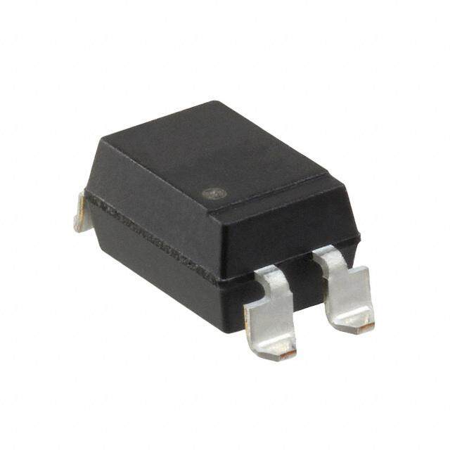
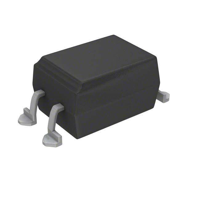
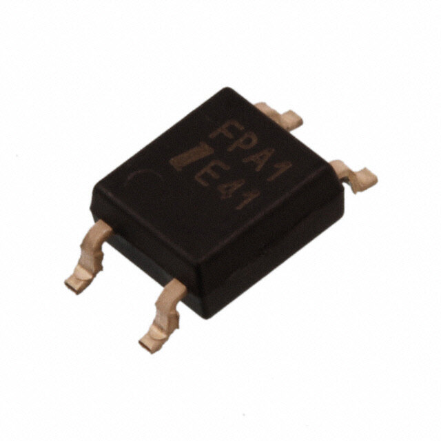
| 描述 | OPTOISO 3.75KV TRANS 4-MINI-FLAT晶体管输出光电耦合器 OptoHiT Series; Hi Temp Phototransistor |
| 产品分类 | |
| 品牌 | Fairchild Semiconductor |
| 产品手册 | |
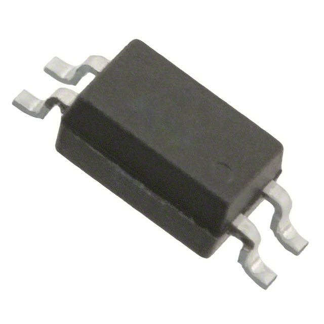
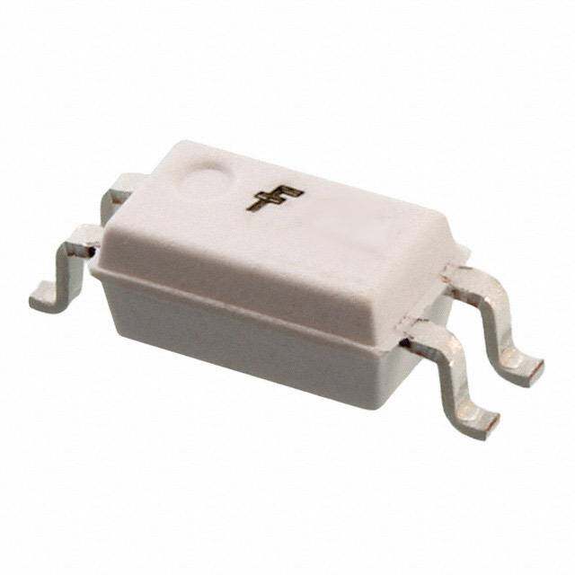
| 产品图片 |
|
| rohs | 符合RoHS无铅 / 符合限制有害物质指令(RoHS)规范要求 |
| 产品系列 | 光耦合器/光电耦合器,晶体管输出光电耦合器,Fairchild Semiconductor FODM8801BVOptoHit™ |
| 数据手册 | |
| 产品型号 | FODM8801BV |
| Vce饱和值(最大值) | 400mV |
| 上升/下降时间(典型值) | 5µs, 5.5µs |
| 产品种类 | 晶体管输出光电耦合器 |
| 供应商器件封装 | 4-Mini-Flat |
| 包装 | 散装 |
| 单位重量 | 120 mg |
| 商标 | Fairchild Semiconductor |
| 安装类型 | 表面贴装 |
| 封装 | Bulk |
| 封装/外壳 | 4-SOIC (0.173", 4.40mm) |
| 封装/箱体 | Mini Flat-4 |
| 工作温度 | -40°C ~ 125°C |
| 工厂包装数量 | 3000 |
| 打开/关闭时间(典型值) | 6µs, 6µs |
| 最大上升时间 | 5 us |
| 最大下降时间 | 5.5 us |
| 最大功率耗散 | 40 mW |
| 最大工作温度 | + 125 C |
| 最大正向二极管电压 | 1.8 V |
| 最大输入二极管电流 | 200 mA |
| 最大集电极/发射极饱和电压 | 0.4 V |
| 最大集电极电流 | 30 mA |
| 最小工作温度 | - 40 C |
| 标准包装 | 3,000 |
| 正向电流 | 1 mA to 10 mA |
| 每芯片的通道数量 | 1 Channel |
| 电压-正向(Vf)(典型值) | 1.35V |
| 电压-输出(最大值) | 75V |
| 电压-隔离 | 3750Vrms |
| 电流-DC正向(If) | 20mA |
| 电流-输出/通道 | 30mA |
| 电流传输比(最大值) | 360% @ 1mA |
| 电流传输比(最小值) | 65% @ 1mA |
| 电流传递比 | 195 % |
| 系列 | FODM8801B |
| 绝缘电压 | 3750 Vrms |
| 输入类型 | DC |
| 输出类型 | DC |
| 输出设备 | Phototransistor |
| 通道数 | 1 |


- 商务部:美国ITC正式对集成电路等产品启动337调查
- 曝三星4nm工艺存在良率问题 高通将骁龙8 Gen1或转产台积电
- 太阳诱电将投资9.5亿元在常州建新厂生产MLCC 预计2023年完工
- 英特尔发布欧洲新工厂建设计划 深化IDM 2.0 战略
- 台积电先进制程称霸业界 有大客户加持明年业绩稳了
- 达到5530亿美元!SIA预计今年全球半导体销售额将创下新高
- 英特尔拟将自动驾驶子公司Mobileye上市 估值或超500亿美元
- 三星加码芯片和SET,合并消费电子和移动部门,撤换高东真等 CEO
- 三星电子宣布重大人事变动 还合并消费电子和移动部门
- 海关总署:前11个月进口集成电路产品价值2.52万亿元 增长14.8%
PDF Datasheet 数据手册内容提取
Is Now Part of To learn more about ON Semiconductor, please visit our website at www.onsemi.com Please note: As part of the Fairchild Semiconductor integration, some of the Fairchild orderable part numbers will need to change in order to meet ON Semiconductor’s system requirements. Since the ON Semiconductor product management systems do not have the ability to manage part nomenclature that utilizes an underscore (_), the underscore (_) in the Fairchild part numbers will be changed to a dash (-). This document may contain device numbers with an underscore (_). Please check the ON Semiconductor website to verify the updated device numbers. The most current and up-to-date ordering information can be found at www.onsemi.com. Please email any questions regarding the system integration to Fairchild_questions@onsemi.com. ON Semiconductor and the ON Semiconductor logo are trademarks of Semiconductor Components Industries, LLC dba ON Semiconductor or its subsidiaries in the United States and/or other countries. ON Semiconductor owns the rights to a number of patents, trademarks, copyrights, trade secrets, and other intellectual property. A listing of ON Semiconductor’s product/patent coverage may be accessed at www.onsemi.com/site/pdf/Patent-Marking.pdf. ON Semiconductor reserves the right to make changes without further notice to any products herein. ON Semiconductor makes no warranty, representation or guarantee regarding the suitability of its products for any particular purpose, nor does ON Semiconductor assume any liability arising out of the application or use of any product or circuit, and specifically disclaims any and all liability, including without limitation special, consequential or incidental damages. Buyer is responsible for its products and applications using ON Semiconductor products, including compliance with all laws, regulations and safety requirements or standards, regardless of any support or applications information provided by ON Semiconductor. “Typical” parameters which may be provided in ON Semiconductor data sheets and/or specifications can and do vary in different applications and actual performance may vary over time. All operating parameters, including “Typicals” must be validated for each customer application by customer’s technical experts. ON Semiconductor does not convey any license under its patent rights nor the rights of others. ON Semiconductor products are not designed, intended, or authorized for use as a critical component in life support systems or any FDA Class 3 medical devices or medical devices with a same or similar classification in a foreign jurisdiction or any devices intended for implantation in the human body. Should Buyer purchase or use ON Semiconductor products for any such unintended or unauthorized application, Buyer shall indemnify and hold ON Semiconductor and its officers, employees, subsidiaries, affiliates, and distributors harmless against all claims, costs, damages, and expenses, and reasonable attorney fees arising out of, directly or indirectly, any claim of personal injury or death associated with such unintended or unauthorized use, even if such claim alleges that ON Semiconductor was negligent regarding the design or manufacture of the part. ON Semiconductor is an Equal Opportunity/Affirmative Action Employer. This literature is subject to all applicable copyright laws and is not for resale in any manner.
F O D M May 2017 8 8 0 1 X — FODM8801A, FODM8801B, FODM8801C O p OptoHiT™ Series, High-Temperature Phototransistor t o H Optocoupler in Half-Pitch Mini-Flat 4-Pin Package i T ™ S Features Description e r i e • Utilizing Proprietary Process Technology to Achieve In the OptoHiT™ series, the FODM8801 is a first-of-kind s , High Operating Temperature: up to 125°C phototransistor, utilizing Fairchild’s leading-edge H • Guaranteed Current Transfer Ratio (CTR) proprietary process technology to achieve high operating ig Specifications Across Full Temperature Range temperature characteristics, up to 125°C. The opto- h - coupler consists of an aluminum gallium arsenide T –Excellent CTR Linearity at High-Temperature e (AlGaAs) infrared light-emitting diode (LED) optically m –CTR at Very Low Input Current, IF coupled to a phototransistor, available in a compact half- p e • High Isolation Voltage Regulated by Safety Agency: pitch, mini-flat, 4-pin package. It delivers high current r a C-UL / UL1577, 3750 VACRMS for 1 minute and transfer ratio at very low input current. The input-output tu DIN EN/IEC60747-5-5 isolation voltage, VISO, is rated at 3750 VACRMS. re • Compact Half-Pitch, Mini-Flat, 4-Pin Package P h (1.27 mm Lead Pitch, 2.4 mm Maximum Standoff o Height) to t • > 5 mm Creepage and Clearance Distance r a • Applicable to Infrared Ray Reflow, 245°C n s i s Applications t o r • Primarily Suited for DC-DC Converters O p • Ground-Loop Isolation, Signal-Noise Isolation t o • Communications – Adapters, Chargers c o • Consumer – Appliances, Set-Top Boxes u p • Industrial – Power Supplies, Motor Control, le r Programmable Logic Control i n H a l f - Schematic Package P i t c h M i n ANODE 1 4 COLLECTOR i - F l a t 4 CATHODE 2 3 EMITTER -P i n Figure 2. Half-Pitch Mini-Flat P a Figure 1. Schematic c k a g e ©2010 Fairchild Semiconductor Corporation www.fairchildsemi.com FODM8801X Rev. 1.2
F O Safety and Insulation Ratings D M As per DIN EN/IEC 60747-5-5, this optocoupler is suitable for “safe electrical insulation” only within the safety limit 8 8 data. Compliance with the safety ratings shall be ensured by means of protective circuits. 0 1 X Parameter Characteristics — Installation Classifications per DIN VDE < 150 VRMS I–IV O 0110/1.89 Table 1, For Rated Mains Voltage < 300 VRMS I–III pto Climatic Classification 40/125/21 H i T Pollution Degree (DIN VDE 0110/1.89) 2 ™ Comparative Tracking Index 175 S e r i e s , Symbol Parameter Value Unit H i g Input-to-Output Test Voltage, Method A, V x 1.6 = V , h Type and Sample Test with t = 10 s, PartIiOaRl DMischarge <P R5 pC 848 Vpeak -T V m e PR m Input-to-Output Test Voltage, Method B, V x 1.875 = V , 100% Production Test with tm = 1 s, PartiaIlO DRiMscharge < 5 pPCR 1060 Vpeak pe r V Maximum Working Insulation Voltage 565 V a IORM peak t u V Highest Allowable Over-Voltage 6000 V r IOTM peak e External Creepage 5 mm P h o External Clearance 5 mm t o DTI Distance Through Insulation (Insulation Thickness) 0.5 mm tr a T Case Temperature(1) 150 °C n S s I Input Current(1) 200 mA is S,INPUT t o P Output Power(1) 300 mW r S,OUTPUT O RIO Insulation Resistance at TS, VIO = 500 V(1) >109 p t o Note: c o 1. Safety limit values – maximum values allowed in the event of a failure. u p l e r i n H a l f - P i t c h M i n i - F l a t 4 - P i n P a c k a g e ©2010 Fairchild Semiconductor Corporation www.fairchildsemi.com FODM8801X Rev. 1.2 2
F O Absolute Maximum Ratings D M Stresses exceeding the absolute maximum ratings may damage the device. The device may not function or be 8 8 operable above the recommended operating conditions and stressing the parts to these levels is not recommended. 0 1 In addition, extended exposure to stresses above the recommended operating conditions may affect device reliability. X The absolute maximum ratings are stress ratings only. T = 25°C unless otherwise specified. — A O Symbol Parameter Value Unit p t o Total Package H TSTG Storage Temperature -40 to +150 °C iT ™ TOPR Operating Temperature -40 to +125 °C S TJ Junction Temperature -40 to +140 °C er i e TSOL Lead Solder Temperature 245 for 10 s °C s , Emitter H i g IF(average) Continuous Forward Current 20 mA h - T VR Reverse Input Voltage 6 V e m PDLED Power Dissipation(2)(4) 40 mW p e Detector ra t IC(average) Continuous Collector Current 30 mA ur e VCEO Collector-Emitter Voltage 75 V P h VECO Emitter-Collector Voltage 7 V o t o PDC Collector Power Dissipation(3)(4) 150 mW tr a Notes: n s 2.Derate linearly from 73°C at a rate of 0.24 mW/°C is t o 3.Derate linearly from 73°C at a rate of 2.23 mW/°C. r O 4.Functional operation under these conditions is not implied. Permanent damage may occur if the device is subjected p to conditions outside these ratings. t o c Recommended Operating Conditions o u p The Recommended Operating Conditions table defines the conditions for actual device operation. Recommended le operating conditions are specified to ensure optimal performance to the datasheet specifications. Fairchild does not r i recommend exceeding them or designing to absolute maximum ratings. n H a Symbol Parameter Value Unit l f - P TA Operating Temperature -40 to +125 °C it c VFL(OFF) Input Low Voltage -5.0 to +0.8 V h M IFH Input High Forward Current 1 to 10 mA in i - F l a Isolation Characteristics t 4 - P Symbol Parameter Conditions Min. Typ. Max. Unit i n P VISO Input-Output Isolation Voltage f = 60 Hz, t = 1 min., II-O 10 µA(5)(6) 3,750 VACRMS a c RISO Isolation Resistance VI-O = 500 V(5) 1012 ka g CISO Isolation Capacitance f = 1 MHz 0.3 0.5 pF e Notes: 5.Device is considered a two-terminal device: pins 1 and 2 are shorted together and pins 3 and 4 are shorted together. 6.3,750 VAC for 1 minute is equivalent to 4,500 VAC for 1 second. RMS RMS ©2010 Fairchild Semiconductor Corporation www.fairchildsemi.com FODM8801X Rev. 1.2 3
F O Electrical Characteristics D M Apply over all recommended conditions (TA = -40°C to +125°C unless otherwise specified). 8 All typical values are measured at T = 25°C. 8 A 0 1 X Symbol Parameter Conditions Min. Typ. Max. Unit — Emitter O p VF Forward Voltage IF = 1 mA 1.00 1.35 1.80 V to H VF / TA Forward-Voltage Coefficient IF = 1 mA -1.6 mV / °C iT ™ IR Reverse Current VR = 6 V 10 µA S CT Terminal Capacitance V = 0 V, f = 1 MHz 30 pF e r i Detector e s , Collector-Emitter Breakdown H BVCEO Voltage IC = 0.5 mA, IF = 0 mA 75 130 V ig h BVECO EVomltiattgeer- Collector Breakdown IE = 100 µA, IF = 0 mA 7 12 V -Te m V = 75 V, I = 0 mA, p CE F 100 nA e T = 25°C r A a ICEO Collector Dark Current VCE = 50 V, IF = 0 mA 50 µA tur e VCE = 5 V, IF = 0 mA 30 µA Ph o CCE Capacitance VCE = 0 V, f = 1 MHz 8 pF t o t r a n s i s t o r O p t o c o u p l e r i n H a l f - P i t c h M i n i - F l a t 4 - P i n P a c k a g e ©2010 Fairchild Semiconductor Corporation www.fairchildsemi.com FODM8801X Rev. 1.2 4
F O D Transfer Characteristics M Apply over all recommended conditions (T = -40°C to +125°C unless otherwise specified). 8 A 8 All typical values are measured at T = 25°C. 0 A 1 X Symbol Parameter Device Conditions Min. Typ. Max. Unit — IF = 1.0 mA, VCE = 5 V O 80 120 160 p @ T = 25°C A t o FODM8801A IF = 1.0 mA, VCE = 5 V 35 120 230 Hi T IF = 1.6 mA, VCE = 5 V 40 125 ™ IF = 3.0 mA, VCE = 5 V 45 138 Se r I = 1.0 mA, V = 5 V i F CE e @ T = 25°C 130 195 260 s Current Transfer A , H CTRCE Ratio FODM8801B IF = 1.0 mA, VCE = 5 V 65 195 360 % ig (Collector-Emitter) IF = 1.6 mA, VCE = 5 V 70 202 h-T e IF = 3.0 mA, VCE = 5 V 75 215 m p I = 1.0 mA, V = 5 V F CE e 200 300 400 r @ TA = 25°C a t u FODM8801C IF = 1.0 mA, VCE = 5 V 100 300 560 re IF = 1.6 mA, VCE = 5 V 110 312 P h IF = 3.0 mA, VCE = 5 V 115 330 ot o I = 1.0 mA, V = 0.4 V t F CE r 65 108 150 a @ TA = 25°C n s FODM8801A IF = 1.0 mA, VCE = 0.4 V 30 108 is t o IF = 1.6 mA, VCE = 0.4 V 25 104 r O IF = 3.0 mA, VCE = 0.4 V 20 92 p t o I = 1.0 mA, V = 0.4 V F CE c @ T = 25°C 90 168 245 o A u Saturated Current p CTRCE(SAT) Transfer Ratio FODM8801B IF = 1.0 mA, VCE = 0.4 V 45 168 % le (Collector-Emitter) IF = 1.6 mA, VCE = 0.4 V 40 155 r in IF = 3.0 mA, VCE = 0.4 V 35 132 H a IF = 1.0 mA, VCE = 0.4 V 140 238 380 lf-P @ T = 25°C A it c FODM8801C IF = 1.0 mA, VCE = 0.4 V 75 238 h M IF = 1.6 mA, VCE = 0.4 V 65 215 in IF = 3.0 mA, VCE = 0.4 V 55 177 i-F l IF = 1.0 mA, IC = 0.3 mA 0.17 0.40 at 4 FODM8801A IF = 1.6 mA, IC = 0.4 mA 0.16 0.40 -P IF = 3.0 mA, IC = 0.6 mA 0.15 0.40 in P IF = 1.0 mA, IC = 0.45 mA 0.17 0.40 a c VCE(SAT) Saturation Voltage FODM8801B IF = 1.6 mA, IC = 0.6 mA 0.16 0.40 V ka g IF = 3.0 mA, IC = 1.0 mA 0.16 0.40 e IF = 1.0 mA, IC = 0.75 mA 0.18 0.40 FODM8801C IF = 1.6 mA, IC = 1.0 mA 0.17 0.40 IF = 3.0 mA, IC = 1.6 mA 0.17 0.40 ©2010 Fairchild Semiconductor Corporation www.fairchildsemi.com FODM8801X Rev. 1.2 5
F O Switching Characteristics D M Apply over all recommended conditions (T = -40°C to +125°C unless otherwise specified). 8 A 8 All typical values are measured at T = 25°C. 0 A 1 X Symbol Parameter Device Conditions Min. Typ. Max. Unit — I = 1.6 mA, V = 5 V, O F CC 1 6 20 p tON Turn-On Time All Devices RI L = = 1 0.6.7 m5 Ak, V = 5 V, µs toH F CC 6 iT RL = 4.7 k ™ I = 1.6 mA, V = 5 V, S F CC 1 6 20 e tOFF Turn-Off Time All Devices RL = 0.75 k µs rie I = 1.6 mA, V = 5 V, s F CC 40 , R = 4.7 k H L i g tR O(1u0t%pu tto R 9is0e% T) ime All Devices IRF = = 1 0.6.7 m5 Ak, V CC = 5 V, 5 µs h-T L e m Output Fall Time I = 1.6 mA, V = 5 V, tF (90% to 10%) All Devices RFL = 0.75 k CC 5.5 µs per a Common-Mode TA = 25°C, IF = 0 mA, tu r CMH R(Terajencstiioenn tV Imoltmaguen ity) – All Devices VVO > =2 .100 V0,0 R VL( 7=) ,4.7 k, 20 kV / µs e P CM h Output High Figure 16 o t o Common-Mode TA = 25°C, IF = 1.6 mA, tr a CML R(Terajencstiioenn tV Imoltmaguen ity) – All Devices VVOCM < =0 .180 V0,0 R VL( 7=) ,4.7 k, 20 kV / µs nsis Output Low Figure 16 to r Note: O p 7.Common-mode transient immunity at output high is the maximum tolerable positive dVcm/dt on the leading edge of t o the common-mode impulse signal, V , to assure that the output remains high. c CM o u p l e r i n H a l f - P i t c h M i n i - F l a t 4 - P i n P a c k a g e ©2010 Fairchild Semiconductor Corporation www.fairchildsemi.com FODM8801X Rev. 1.2 6
F O Typical Performance Curves D M 100 100 8 8 TA = 25°C 0 1 NT (mA) ENT (mA) VCE = 5.0 V X — O RE 10 RR 10 p UR CU VCE = 0.4 V to WARD C TA = 125°C = 25°C ECTOR HiT™ OR 1.0 TA = -40°C OLL 1.0 S I– FF – C IC eries , H i g 0.1 0.1 h 1.0 1.1 1.2 1.3 1.4 1.5 1.6 1.7 1.8 0.1 1 10 100 - T VF – FORWARD VOLTAGE (V) IF – FORWARD CURRENT (mA) e m Figure 3. Forward Current vs. Forward Voltage Figure 4. Collector Current vs. Forward Current p e r a 1000 10 t R RATIO (%) VTAC E= =2 55° VC CTR(I= 1mA) F VTNACO E=R =M2 55A° LVCIZED TO IF = 1mA ure Photo NT TRANSFE 100 D) = CTR(I) / F 1.0 transist URRE ALIZE or O – C RM p TR NO to C R ( co CT u p 10 0.1 l 0.1 1 10 100 0.1 1 10 100 e r IF – FORWARD CURRENT (mA) IF – FORWARD CURRENT (mA) in Figure 5. Current Transfer Ratio vs. Forward Current Figure 6. Normalized CTR vs. Forward Current H a l f - 1.2 1.2 P VCE = 2 V VCE = 5 V itc h 1.0 IF = 2 mA 1.0 IF = 2 mA M 5°C 5°C in R @ 2 0.8 IF = 0.5mA R @ 2 0.8 IF = 0.5 mA i-Fl T T a D C 0.6 IF = 1 mA D C 0.6 IF = 1 mA t 4 E E - Z Z P ALI ALI in RM 0.4 RM 0.4 P O O N N a c 0.2 0.2 k a g e 0 0 -40 -20 0 20 40 60 80 100 120 140 -40 -20 0 20 40 60 80 100 120 140 TA – AMBIENT TEMPERATURE (°C) TA – AMBIENT TEMPERATURE (°C) Figure 7. Normalized CTR vs. Ambient Temperature Figure 8. Normalized CTR vs. Ambient Temperature ©2010 Fairchild Semiconductor Corporation www.fairchildsemi.com FODM8801X Rev. 1.2 7
F O Typical Performance Curves (Continued) D M 100 40 8 VCE = 5 V TA = 25°C 80 35 1 I– COLLECTOR CURRENT (mA)C 11.00 IIIIIFIIFFFFFF = ====== 5 132011.0.0.0..0560 m m m mmmmAAAAAAA I– COLLECTOR CURRENT (mA)C 3221105050 IF = 20 mA IFIIFF = == 1 1550 mm mAAA X — OptoHiT™ Serie 5 s IF = 1 mA , H 0.1 0 i -40 -20 0 20 40 60 80 100 120 0 1 2 3 4 5 g h TA – AMBIENT TEMPERATURE (°C) VCE – COLLECTOR-EMITTER VOLTAGE (V) -T Figure 9. Collector Current vs. Figure 10 Collector Current vs. e m Ambient Temperature Collector-Emitter Voltage p e r 100000 1000 a t NT (nA) 10000 VCE = 75 V VTIFAC = E= 1 =2. 655 ° mVCA ure P RE 100 h R 1000 s) tOFF o CTOR DARK CU 10100 VCE = 10 V VCE =V 2C4E V = 48 V TCHING TIME (μ 10 tF tON totransis LE WI to OL 1 S tR r C 1 O – CEO 0.1 VCE = 5 V pto I c o 0.01 0.1 u -40 -20 0 20 40 60 80 100 120 100 10 100 p TA – AMBIENT TEMPERATURE (°C) RL – LOAD RESISTANCE (kΩ) le r Figure 11. Collector Dark Current vs. Figure 12. Switching Time vs. Load Resistance in Ambient Temperature H a l 0.35 300 f- P VCE = 5 V, IF = 3 mA it V– COLLECTOR-EMITTERCE(SAT) SATURATION VOLTAGE (V) 000000......322110050505 IF = 1.6 mA, IC = 1.6 mIAF = 3.0 mA, IC = 1.8 mA CTR – CURRENT TRANSFER RATIO (%) 221150500000 VCE = V0.C4VE V C=,E I0 F= . 4 =0 V.34, mVIF,A =I F 1 =.6 1 m mVAAC EV C=E 5 = V 5, IVF, =IF 1 = m 1A.6 mA ch Mini-Flat 4-Pin Pack a g 0.00 50 e -40 -20 0 20 40 60 80 100 120 -40 -20 0 20 40 60 80 100 120 TA – AMBIENT TEMPERATURE (°C) TA – AMBIENT TEMPERATURE (°C) Figure 13. Collector-Emitter Saturation Voltage Figure 14. Current Transfer Ration vs. vs. Ambient Temperature Ambient Temperature ©2010 Fairchild Semiconductor Corporation www.fairchildsemi.com FODM8801X Rev. 1.2 8
F O Test Circuits D M 8 +5 V 8 0 1 RL = 4.7 kΩ X P tur ls=e 5 G nesnerator: IF + 1 4 VO VO Monitoring Node — O ZO = 50 Ω p PW = 50 μs to DC = 1% GND H IF Monitor 2 3 iT ™ RM S e r i e s (IF = 1.6 mA) , H Input Pulse ig h - T tR tF em 5 V p 90% e Output Pulse r a 10% t u VOL r e tON tOFF P h o Figure 15. Test Circuit for Propagation Delay, Rise Time, and Fall Time t o t r a n +5 V s i s t o RL = 4.7 kΩ r IF + O 1 4 VO Monitoring Node p t o c SW o GND u 2 3 p l e RM r i n VCM H a l Pulse Gen f- P i VCM 90% 1 kV tc h M 10% 0 V in i - F l a t 4 VOH - VO (IF = 0 mA) 2 V Pin P a 0.8 V c VO (IF = 1.6 mA) ka VOL g e Figure 16. Test Circuit for Instantaneous Common-Mode Rejection Voltage ©2010 Fairchild Semiconductor Corporation www.fairchildsemi.com FODM8801X Rev. 1.2 9
F O Reflow Profile D M 8 8 0 1 Max. Ramp-up Rate = 3°C/S X 226405 TP Max. Ramp-down Rate = 6°C/S — 240 O tP 220 TL pt o 200 Tsmax H i T ) 180 tL ™ C ° S (e 160 Tsmin er ur 140 ts ie t s ar 120 , H e p 100 ig m h Te 80 -Te 60 m p 40 e r a 20 tu r 0 e P 120 240 360 h o Time 25°C to Peak t o t r Figure 13. Reflow Profile a n s Profile Freature Pb-Free Assembly Profile is t o Temperature Minimum (Tsmin) 150°C r O Temperature Maximum (Tsmax) 200°C p t Time (t ) from (Tsmin to Tsmax) 60–120 seconds o S c o Ramp-up Rate (tL to tP) 3°C/second maximum u p Liquidous Temperature (T ) 217°C l L e r Time (tL) Maintained Above (TL) 60–150 seconds in Peak Body Package Temperature 245°C +0°C / –5°C H a Time (tP) within 5°C of 245°C 30 seconds lf- P Ramp-down Rate (TP to TL) 6°C/second maximum it c Time 25°C to Peak Temperature 8 minutes maximum h M i n i - F Figure 17. Reflow Profile l a t 4 - P i n P a c k a g e ©2010 Fairchild Semiconductor Corporation www.fairchildsemi.com FODM8801X Rev. 1.2 10
F O Ordering Information D M 8 Part Number Package Packing Method 8 0 FODM8801A Half Pitch Mini-Flat 4-Pin Tube (100 units) 1 X FODM8801AR2 Half Pitch Mini-Flat 4-Pin Tape and Reel (2500 Units) — FODM8801AV Half Pitch Mini-Flat 4-Pin, DIN EN/IEC60747-5-5 Option Tube (100 Units) O p FODM8801AR2V Half Pitch Mini-Flat 4-Pin, DIN EN/IEC60747-5-5 Option Tape and Reel (2500 Units) t o H Note: iT ™ 8. The product orderable part number system listed in this table also applies to the FODM8801B, FODM8801C prod- ucts. S e r i e s Marking Information , H i g h - T 1 e m p 8801x 2 er a t u V X YY M1 6 re P h 3 o 4 5 t o t r a n Figure 18. Top Mark s i s t o r Table 1. Top Mark Definitions O p 1 Fairchild Logo to c 2 Device Number o u 3 DIN EN/IEC60747-5-5 Option (only appears on component ordered with this option) p l e 4 One-Digit Year Code, e.g., “6” r i n 5 Digit Work Week, Ranging from “01” to “53” H 6 Assembly Package Code a l f - P i t c h M i n i - F l a t 4 - P i n P a c k a g e ©2010 Fairchild Semiconductor Corporation www.fairchildsemi.com FODM8801X Rev. 1.2 11
F O Tape and Reel Dimensions D M 8 8 P D 0 2 0 1 K0 t P0 E X — O p t o A H 0 W W1 B0 F iT™ S e r i d P D1 es , H i g h 1.27 Pitch - T e Description Symbol Dimensions (mm) m Tape Width W 12.00 +0.30/-0.10 p e r Tape Thickness t 0.30 ±0.05 a t u Sprocket Hole Pitch P0 4.00 ±0.10 re Sprocket Hole Diameter D0 1.50 +0.10 / -0.0 P h Sprocket Hole Location E 1.75 ±0.10 o t Pocket Location F 5.50 ±0.10 ot r P2 2.00 ±0.10 an s Pocket Pitch P 8.00 ±0.10 i s t Pocket Dimension A 2.80 ±0.10 o 0 r B 7.30 ±0.10 O 0 p K0 2.30 ±0.10 to c Pocket Hole Diameter D1 1.50 Min. o u Cover Tape Width W 9.20 p 1 l e Cover Tape Thickness d 0.065 ±0.010 r i Max. Component Rotation or Tilt 10° Max. n H Devices Per Reel 2500 a l f - Reel Diameter 330 mm (13") P i t c h M i n i - F l a t 4 - P i n P a c k a g e ©2010 Fairchild Semiconductor Corporation www.fairchildsemi.com FODM8801X Rev. 1.2 12
0.3-0.51 2 1 PINONE 0.61 2 5 . 9 ) 1 2 p . y 7 T 0- 0( 3 4 6. 4. 7 3 8 8 7. 4. 3 4 0.55-0.75 2.31-2.69 1.27 2.39(Max) LANDPATTERNRECOMMENDATION 1.95-2.11 0-0.20 R0.15(Typ) (cid:19)(cid:131)(cid:97)(cid:27)(cid:131) R0.15(Typ) 1.27+-.127 0.30-0.89 0.18-0.25 1.19(Typ) NOTES: A) NOSTANDARDAPPLIESTOTHISPACKAGE B)ALLDIMENSIONSAREINMILLIMETERS. C)DIMENSIONSAREEXCLUSIVEOFBURRS, MOLDFLASH,ANDTIEBAREXTRUSION D)DRAWINGFILENAMEANDREVSION:MKT-MFP04AREV4.
ON Semiconductor and are trademarks of Semiconductor Components Industries, LLC dba ON Semiconductor or its subsidiaries in the United States and/or other countries. ON Semiconductor owns the rights to a number of patents, trademarks, copyrights, trade secrets, and other intellectual property. A listing of ON Semiconductor’s product/patent coverage may be accessed at www.onsemi.com/site/pdf/Patent−Marking.pdf. ON Semiconductor reserves the right to make changes without further notice to any products herein. ON Semiconductor makes no warranty, representation or guarantee regarding the suitability of its products for any particular purpose, nor does ON Semiconductor assume any liability arising out of the application or use of any product or circuit, and specifically disclaims any and all liability, including without limitation special, consequential or incidental damages. Buyer is responsible for its products and applications using ON Semiconductor products, including compliance with all laws, regulations and safety requirements or standards, regardless of any support or applications information provided by ON Semiconductor. “Typical” parameters which may be provided in ON Semiconductor data sheets and/or specifications can and do vary in different applications and actual performance may vary over time. All operating parameters, including “Typicals” must be validated for each customer application by customer’s technical experts. ON Semiconductor does not convey any license under its patent rights nor the rights of others. ON Semiconductor products are not designed, intended, or authorized for use as a critical component in life support systems or any FDA Class 3 medical devices or medical devices with a same or similar classification in a foreign jurisdiction or any devices intended for implantation in the human body. Should Buyer purchase or use ON Semiconductor products for any such unintended or unauthorized application, Buyer shall indemnify and hold ON Semiconductor and its officers, employees, subsidiaries, affiliates, and distributors harmless against all claims, costs, damages, and expenses, and reasonable attorney fees arising out of, directly or indirectly, any claim of personal injury or death associated with such unintended or unauthorized use, even if such claim alleges that ON Semiconductor was negligent regarding the design or manufacture of the part. ON Semiconductor is an Equal Opportunity/Affirmative Action Employer. This literature is subject to all applicable copyright laws and is not for resale in any manner. PUBLICATION ORDERING INFORMATION LITERATURE FULFILLMENT: N. American Technical Support: 800−282−9855 Toll Free ON Semiconductor Website: www.onsemi.com Literature Distribution Center for ON Semiconductor USA/Canada 19521 E. 32nd Pkwy, Aurora, Colorado 80011 USA Europe, Middle East and Africa Technical Support: Order Literature: http://www.onsemi.com/orderlit Phone: 303−675−2175 or 800−344−3860 Toll Free USA/Canada Phone: 421 33 790 2910 Fax: 303−675−2176 or 800−344−3867 Toll Free USA/Canada Japan Customer Focus Center For additional information, please contact your local Email: orderlit@onsemi.com Phone: 81−3−5817−1050 Sales Representative © Semiconductor Components Industries, LLC www.onsemi.com www.onsemi.com 1
Mouser Electronics Authorized Distributor Click to View Pricing, Inventory, Delivery & Lifecycle Information: O N Semiconductor: FODM8801B FODM8801BR2 FODM8801BR2V FODM8801BV