ICGOO在线商城 > 隔离器 > 光隔离器 - 晶体管,光电输出 > FODM121A

 Datasheet下载
- 型号: FODM121A
- 制造商: Fairchild Semiconductor
- 库位|库存: xxxx|xxxx
- 要求:
| 数量阶梯 | 香港交货 | 国内含税 |
| +xxxx | $xxxx | ¥xxxx |
查看当月历史价格
查看今年历史价格
FODM121A产品简介:
ICGOO电子元器件商城为您提供FODM121A由Fairchild Semiconductor设计生产,在icgoo商城现货销售,并且可以通过原厂、代理商等渠道进行代购。 FODM121A价格参考。Fairchild SemiconductorFODM121A封装/规格:光隔离器 - 晶体管,光电输出, 光隔离器 晶体管 输出 3750Vrms 1 通道 4-Mini-Flat。您可以下载FODM121A参考资料、Datasheet数据手册功能说明书,资料中有FODM121A 详细功能的应用电路图电压和使用方法及教程。
ON Semiconductor的FODM121A是一款光隔离器,属于光电晶体管类型。它通过光电耦合技术实现输入和输出之间的电气隔离,广泛应用于需要高隔离电压、低功耗和可靠信号传输的场景。以下是FODM121A的主要应用场景:

 1. 工业自动化
   - 在工业控制系统中,FODM121A可用于隔离传感器信号与控制电路,防止噪声干扰或高压损坏敏感电子设备。
   - 例如,用于PLC(可编程逻辑控制器)中的输入/输出接口,确保信号的稳定性和安全性。

 2. 电机驱动与逆变器
   - FODM121A适用于电机驱动电路,特别是在逆变器模块中,用于隔离栅极驱动信号与主控电路。
   - 它能够保护控制电路免受高压开关瞬态的影响,同时提供可靠的信号传输。

 3. 电源管理
   - 在开关电源(SMPS)设计中,FODM121A可以用于反馈回路的隔离,确保初级侧和次级侧的电气安全。
   - 它还能在DC-DC转换器中提供隔离功能,避免高压对低压电路的损害。

 4. 医疗设备
   - 在医疗设备中,如心电图仪、血压监测仪等,FODM121A可用于隔离患者接触部分与设备内部电路,确保患者和操作人员的安全。
   - 其高隔离性能符合医疗设备的严格安全标准。

 5. 通信系统
   - 在通信设备中,FODM121A可用于隔离数字信号,减少电磁干扰(EMI)对信号质量的影响。
   - 它适合于需要长距离信号传输且要求电气隔离的应用。

 6. 汽车电子
   - 在汽车电子系统中,FODM121A可用于隔离电池管理系统(BMS)、发动机控制单元(ECU)和其他关键组件之间的信号。
   - 它能有效防止高压电路对低电压控制电路的干扰。

 7. 家用电器
   - 在家用电器(如洗衣机、空调、冰箱等)中,FODM121A可用于隔离主控板与功率驱动电路,提高系统的可靠性和安全性。

 总结
FODM121A凭借其高隔离电压(通常超过2500Vrms)、快速响应时间和低功耗特性,成为许多高可靠性应用的理想选择。无论是工业、医疗还是消费电子领域,它都能提供有效的电气隔离解决方案,确保系统稳定运行并保护关键组件免受损坏。
| 参数 | 数值 |
| 产品目录 | |
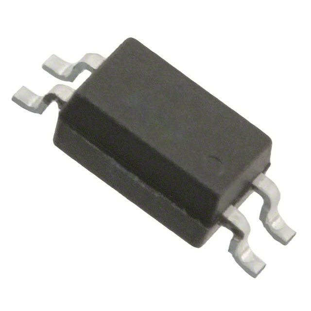
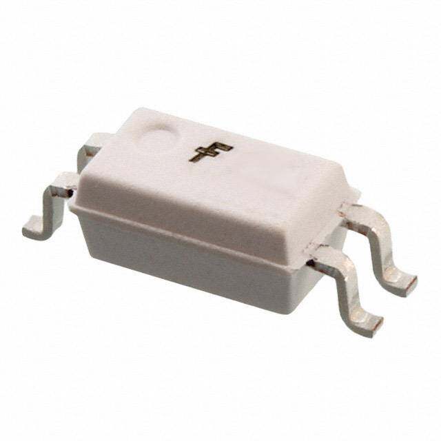
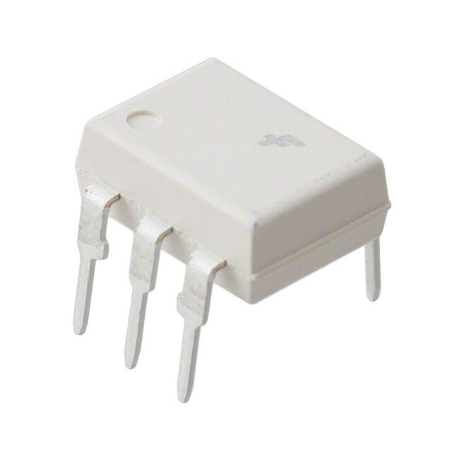
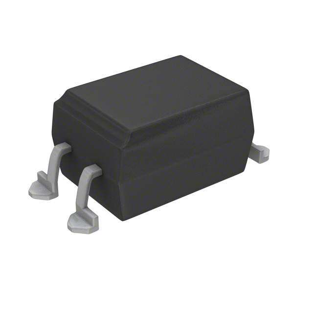
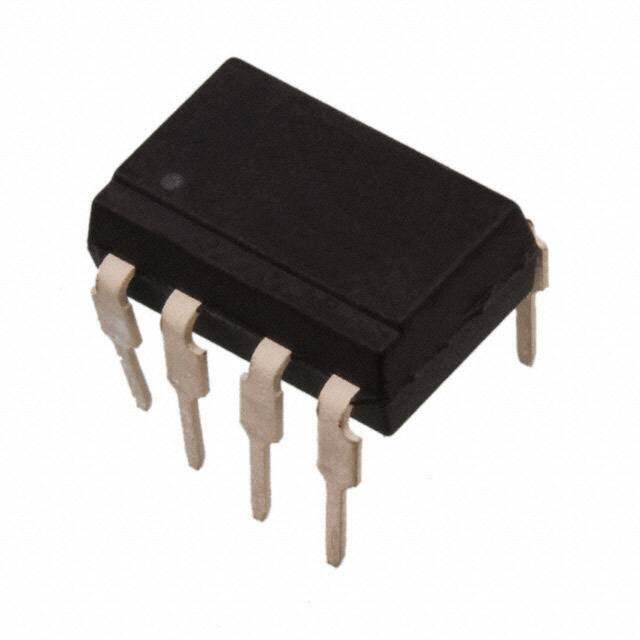
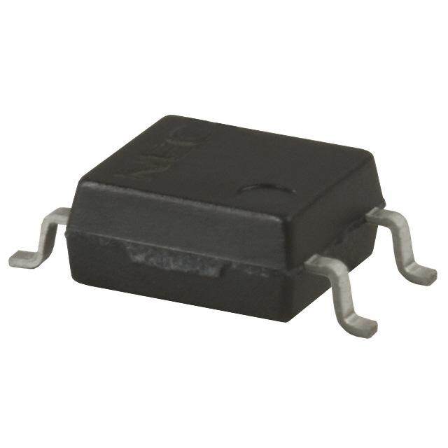
| 描述 | OPTOISO 3.75KV TRANSISTOR 4SMD晶体管输出光电耦合器 Full pitch MFP PhotoTrans Ouput |
| 产品分类 | |
| 品牌 | Fairchild Semiconductor |
| 产品手册 | |
| 产品图片 |
|
| rohs | 符合RoHS无铅 / 符合限制有害物质指令(RoHS)规范要求 |
| 产品系列 | 光耦合器/光电耦合器,晶体管输出光电耦合器,Fairchild Semiconductor FODM121A- |
| 数据手册 | |
| 产品型号 | FODM121A |
| Vce饱和值(最大值) | 400mV |
| 上升/下降时间(典型值) | 3µs, 3µs |
| 产品种类 | 晶体管输出光电耦合器 |
| 供应商器件封装 | 4-SMD |
| 包装 | 管件 |
| 单位重量 | 155 mg |
| 商标 | Fairchild Semiconductor |
| 安装类型 | 表面贴装 |
| 封装 | Bulk |
| 封装/外壳 | 4-SMD,鸥翼型 |
| 封装/箱体 | SMD-4 |
| 工作温度 | -40°C ~ 110°C |
| 工厂包装数量 | 3000 |
| 打开/关闭时间(典型值) | - |
| 最大功率耗散 | 150 mW |
| 最大反向二极管电压 | 6 V |
| 最大工作温度 | + 100 C |
| 最大正向二极管电压 | 1.3 V |
| 最大输入二极管电流 | 50 mA |
| 最大集电极/发射极电压 | 80 V |
| 最大集电极/发射极饱和电压 | 0.4 V |
| 最大集电极电流 | 80 mA |
| 最小工作温度 | - 40 C |
| 标准包装 | 3,000 |
| 每芯片的通道数量 | 1 Channel |
| 电压-正向(Vf)(典型值) | 1.3V (最小值) |
| 电压-输出(最大值) | 80V |
| 电压-隔离 | 3750Vrms |
| 电流-DC正向(If) | 50mA |
| 电流-输出/通道 | 80mA |
| 电流传输比(最大值) | 300% @ 5mA |
| 电流传输比(最小值) | 100% @ 5mA |
| 电流传递比 | 300 % |
| 系列 | FODM121 |
| 绝缘电压 | 3750 Vrms |
| 输入类型 | DC |
| 输出类型 | DC |
| 输出设备 | NPN Phototransistor |
| 通道数 | 1 |
| 配置 | 1 Channel |


.jpg)

PDF Datasheet 数据手册内容提取
Is Now Part of To learn more about ON Semiconductor, please visit our website at www.onsemi.com Please note: As part of the Fairchild Semiconductor integration, some of the Fairchild orderable part numbers will need to change in order to meet ON Semiconductor’s system requirements. Since the ON Semiconductor product management systems do not have the ability to manage part nomenclature that utilizes an underscore (_), the underscore (_) in the Fairchild part numbers will be changed to a dash (-). This document may contain device numbers with an underscore (_). Please check the ON Semiconductor website to verify the updated device numbers. The most current and up-to-date ordering information can be found at www.onsemi.com. Please email any questions regarding the system integration to Fairchild_questions@onsemi.com. ON Semiconductor and the ON Semiconductor logo are trademarks of Semiconductor Components Industries, LLC dba ON Semiconductor or its subsidiaries in the United States and/or other countries. ON Semiconductor owns the rights to a number of patents, trademarks, copyrights, trade secrets, and other intellectual property. A listing of ON Semiconductor’s product/patent coverage may be accessed at www.onsemi.com/site/pdf/Patent-Marking.pdf. ON Semiconductor reserves the right to make changes without further notice to any products herein. ON Semiconductor makes no warranty, representation or guarantee regarding the suitability of its products for any particular purpose, nor does ON Semiconductor assume any liability arising out of the application or use of any product or circuit, and specifically disclaims any and all liability, including without limitation special, consequential or incidental damages. Buyer is responsible for its products and applications using ON Semiconductor products, including compliance with all laws, regulations and safety requirements or standards, regardless of any support or applications information provided by ON Semiconductor. “Typical” parameters which may be provided in ON Semiconductor data sheets and/or specifications can and do vary in different applications and actual performance may vary over time. All operating parameters, including “Typicals” must be validated for each customer application by customer’s technical experts. ON Semiconductor does not convey any license under its patent rights nor the rights of others. ON Semiconductor products are not designed, intended, or authorized for use as a critical component in life support systems or any FDA Class 3 medical devices or medical devices with a same or similar classification in a foreign jurisdiction or any devices intended for implantation in the human body. Should Buyer purchase or use ON Semiconductor products for any such unintended or unauthorized application, Buyer shall indemnify and hold ON Semiconductor and its officers, employees, subsidiaries, affiliates, and distributors harmless against all claims, costs, damages, and expenses, and reasonable attorney fees arising out of, directly or indirectly, any claim of personal injury or death associated with such unintended or unauthorized use, even if such claim alleges that ON Semiconductor was negligent regarding the design or manufacture of the part. ON Semiconductor is an Equal Opportunity/Affirmative Action Employer. This literature is subject to all applicable copyright laws and is not for resale in any manner.
F O D M November 2015 1 2 1 S e FODM121 Series, FODM124, FODM2701, r i e s FODM2705 , F O 4-Pin Full Pitch Mini-Flat Package Phototransistor D M Optocouplers 1 2 4 , Features Applications F O • More than 5 mm Creepage/Clearance • Digital Logic Inputs D M • Compact 4-Pin Surface Mount Package • Microprocessor Inputs 2 (2.4 mm Maximum Standoff Height) • Power Supply Monitor 7 0 • Current Transfer Ratio in Selected Groups: • Twisted Pair Line Receiver 1 , DC Input: • Telephone Line Receiver F O FODM121: 50–600% D Description FODM121A: 100–300% M 2 FODM121B: 50–150% The FODM121 series, FODM124, and FODM2701 7 0 FODM121C: 100–200% consists of a gallium arsenide infrared emitting diode 5 FODM124: 100% MIN driving a phototransistor in a compact 4-pin mini-flat — FODM2701: 50–300% package. The lead pitch is 2.54 mm. The FODM2705 4 AC Input: consists of two gallium arsenide infrared emitting diodes -P FODM2705: 50–300% connected in inverse parallel for AC operation. in F • Safety and Regulatory Approvals: u l – UL1577, 3,750 VACRMS for 1 Minute l P – DIN-EN/IEC60747-5-5, 565 V Peak Working it c Insulation Voltage h M i n i - Functional Block Diagram F l a t P a c ANODE 1 4COLLECTOR k a g e CATHODE2 3EMITTER P h o Equivalent Circuit t o FODM121, FODM124, FODM2701 t r a n s i s ANODE 1 4COLLECTOR Figure 2. Package Outlines to r O CATHODE2 3EMITTER p t o c Equivalent Circuit o FODM2705 u p Figure 1. Schematic le r s ©2006 Fairchild Semiconductor Corporation www.fairchildsemi.com FODM121 Series, FODM124, FODM2701, FODM2705 Rev. 1.7
F O Safety and Insulation Ratings D M As per DIN EN/IEC 60747-5-5, this optocoupler is suitable for “safe electrical insulation” only within the safety limit 1 data. Compliance with the safety ratings shall be ensured by means of protective circuits. 2 1 S Parameter Characteristics e r Installation Classifications per DIN VDE < 150 VRMS I–IV ie s 0110/1.89 Table 1, For Rated Mains Voltage < 300 VRMS I–III , F Climatic Classification 40/110/21 O D Pollution Degree (DIN VDE 0110/1.89) 2 M Comparative Tracking Index 175 1 2 4 , F O Symbol Parameter Value Unit D M Input-to-Output Test Voltage, Method A, V x 1.6 = V , IORM PR 904 V 2 Type and Sample Test with t = 10 s, Partial Discharge < 5 pC peak 7 V m 0 PR Input-to-Output Test Voltage, Method B, V x 1.875 = V , 1 100% Production Test with t = 1 s, PartiaIlO DRiMscharge < 5 pPCR 1060 Vpeak , F m O VIORM Maximum Working Insulation Voltage 565 Vpeak D M V Highest Allowable Over-Voltage 6000 V IOTM peak 2 External Creepage ≥ 5 mm 7 0 External Clearance ≥ 5 mm 5 — DTI Distance Through Insulation (Insulation Thickness) ≥ 0.4 mm 4 TS Case Temperature(1) 150 °C -P i I Input Current(1) 200 mA n S,INPUT F P Output Power(1) 300 mW u S,OUTPUT l l R Insulation Resistance at T , V = 500 V(1) > 109 Ω P IO S IO i t c Note: h 1. Safety limit values – maximum values allowed in the event of a failure. M i n i - F l a t P a c k a g e P h o t o t r a n s i s t o r O p t o c o u p l e r s ©2006 Fairchild Semiconductor Corporation www.fairchildsemi.com FODM121 Series, FODM124, FODM2701, FODM2705 Rev. 1.7 2
F O Absolute Maximum Ratings D Stresses exceeding the absolute maximum ratings may damage the device. The device may not function or be M operable above the recommended operating conditions and stressing the parts to these levels is not recommended. 1 2 In addition, extended exposure to stresses above the recommended operating conditions may affect device reliability. 1 The absolute maximum ratings are stress ratings only. T = 25°C Unless otherwise specified. S A e r Symbol Parameter Value Unit i e s TOTAL PACKAGE , F T Storage Temperature -40 to +125 °C O STG D TOPR Operating Temperature -40 to +110 °C M T Junction Temperature -40 to +125 °C 1 J 2 4 TSOL Lead Solder Temperature 260 for 10 sec °C , F EMITTER O D I Continuous Forward Current 50 mA F (avg) M I Peak Forward Current (1 µs pulse, 300 pps.) 1 A 2 F (pk) 7 V Reverse Voltage 6 V 0 R 1 , Power Dissipation 70 mW F PD O Derate linearly (Above 75°C) 1.41 mW/°C D DETECTOR M 2 I Continuous Collector Current 80 mA 7 C 0 FODM121 Series, FODM124 80 5 VCEO Collector-Emitter Voltage V — FODM2701, FODM2705 40 4 V Emitter-Collector Voltage 6 V - ECO P i Power Dissipation 150 mW n PD F Derate linearly (Above 80°C) 3.27 mW/°C u l l P i t c h M i n i - F l a t P a c k a g e P h o t o t r a n s i s t o r O p t o c o u p l e r s ©2006 Fairchild Semiconductor Corporation www.fairchildsemi.com FODM121 Series, FODM124, FODM2701, FODM2705 Rev. 1.7 3
F O Electrical Characteristics D M TA = 25°C unless otherwise specified. 1 2 1 Symbol Parameter Device Test Conditions Min. Typ. Max. Unit S INDIVIDUAL COMPONENT CHARACTERISTICS e r i Emitter e s , FODM121 Series, F I = 10 mA 1.0 1.3 FODM124 F O V Forward Voltage V D F FODM2701 IF = 5 mA M 1.4 1 FODM2705 I = ±5 mA F 2 4 FODM121 Series, , I Reverse Current FODM124, V = 5 V 5 µA F R R O FODM2701 D M Detector 2 FODM121 Series, 7 80 0 Collector-Emitter FODM124 1 BV I = 1 mA, I = 0 V , CEO Breakdown Voltage FODM2701, C F F 40 O FODM2705 D Emitter-Collector M BVECO Breakdown Voltage All IE = 100 µA, IF = 0 7 V 2 7 0 ICEO Collector Dark Current All VCE = 40 V, IF = 0 100 nA 5 C Capacitance All V = 0 V, f = 1 MHz 10 pF — CE CE TRANSFER CHARACTERISTICS 4 - P FODM2701 I = 5 mA, V = 5 V 50 300 i F CE n FODM2705 I = ±5 mA, V = 5 V 50 300 F F CE u FODM121 50 600 ll P DC Current Transfer FODM121A 100 300 it CTR I = 5 mA, V = 5 V % c Ratio FODM121B F CE 50 150 h M FODM121C 100 200 i n FODM124 IF = 1 mA, VCE = 0.5 V 100 1200 i-F IF = 0.5 mA, VCE = 1.5 V 50 la t CTR Symmetry FODM2705 I = ±5 mA, V = 5 V 0.3 3.0 P F CE a FODM121 Series I = 8 mA, I = 2.4 mA 0.4 c F C k a FODM124 IF = 1 mA, IC = 0.5 mA 0.4 g VCE(SAT) Saturation Voltage V e FODM2701 IF = 10 mA, IC = 2 mA 0.3 P h FODM2705 I = ±10 mA, I = 2 mA 0.3 F C o t Rise Time I = 2 mA, V = 5 V, o tr (Non-Saturated) All RC = 100 Ω CE 3 µs tr L a n t Fall Time All IC = 2 mA, VCE = 5 V, 3 µs s f (Non-Saturated) RL = 100 Ω is t o ISOLATION CHARACTERISTICS r O Steady State Isolation VISO Voltage(2) All 1 minute 3750 VACRMS pt o c Note: o u 2. Steady state isolation voltage, VISO, is an internal device dielectric breakdown rating. For this test, pins 1 and 2 are p common, and pins 3 and 4 are common. le r s ©2006 Fairchild Semiconductor Corporation www.fairchildsemi.com FODM121 Series, FODM124, FODM2701, FODM2705 Rev. 1.7 4
F O Typical Performance Curves D M T = 25°C unless otherwise specified. A 1 2 100 0.35 1 V) S e( e ag 0.30 r I- Forward Current (mA)F10 TA = 1172005oooCCC 0-4o0CoC - Collector-Emitter Saturation Volt 0000....11220505 IIIIFCFC ==== 8122m0.m4mAmAAA ies, FODM124, FO E(sat) 0.05 DM C 1 V 0.00 2 0.6 0.8 1.0 1.2 1.4 1.6 1.8 -40 -20 0 20 40 60 80 100 120 7 VF - Forward Voltage (V) TA - Ambient Temperature (°C) 01 Fig. 3 Forward Current vs. Forward Voltage Fig. 4 Collector-Emitter Saturation Voltage vs. , Ambient Temperature (FODM121/2701/2705) F O 100 D TA = 25oC TA = 25oC M2 %) VCE = 10V 70 TR – Current Transfer Ratio (100 VCE = 5VVCE = 10V I- Collector Current (mA)C110 VCE = 5V 5 — 4-Pin Full P C i t c h 10 0.1 M 0.1 1 10 100 0.1 1 10 100 i Fig. 5 Current ITF r-a Fnosrwfearr dR Cautirore nvts (.m FAo)rward Current Fig. 6 CollecIFt o- rF Coruwrarredn Ctu vrrse.n Ft (omrAw)ard Current ni- F (FODM121/2701/2705) (FODM121/2701/2705) l a t 100 P TA = 25oC a IF = 25mA 40 c IF = 50mA k nt (mA) 10 IF = 5mA IF = 10mA nt (mA) 30 IF = 30mAIF = 40mA age P urre urre IF = 20mA ho or C 1 IF = 1mA or C to ct ct 20 t e e r oll oll IF = 10mA a C C n I- C0.1 IF = 0.5mA - IC 10 IF = 5mA sist o r VCE = 5V IF = 1mA O 0.01 0 p -40 -20 0 20 40 60 80 100 120 0 2 4 6 8 10 t o TA - Ambient Temperature (°C) VCE - Collector-Emitter Voltage (V) c Fig. 7 Collector Current vs. Ambient Temperature Fig. 8 Collector Current vs. Collector-Emitter o u (FODM121/2701/2705) Voltage (FODM121/2701/2705) p l e r s ©2006 Fairchild Semiconductor Corporation www.fairchildsemi.com FODM121 Series, FODM124, FODM2701, FODM2705 Rev. 1.7 5
F O Typical Performance Curves (Continued) D M T = 25°C unless otherwise specified. A 1 10000 160 2 A) 1000 VCE = 40V atio (%) 140 IVFC =E 5=m 5AV Normalized to TA = 25oC 1 Ser n R i nt ( er 120 es urre ansf , F - Collector Dark CCEO 110100 Normalized Current Tr 1680000 ODM124, FO I R – 40 D CT M 0.1 20 2 -40 -20 0 20 40 60 80 100 120 -40 -20 0 20 40 60 80 100 120 7 0 TA - Ambient Temperature (°C) TA - Ambient Temperature (°C) 1 Fig 9. Collector Dark Current vs. Ambient Fig. 10 Normalized Current Transfer Ratio vs. , F Temperature (FODM121/2701/2705) Ambient Temperature (FODM121/2701/2705) O 1000 0.35 D VTAC C= =2 55oVC IF = 5mA IF = 16mA age(V) 0.30 IIFC == 10m.5AmA M27 tOFF Volt 05 e (μs) 100 aturation 0.25 — 4 m S 0.20 - witching Ti tS or-Emitter 0.15 Pin Fu S 10 ollect 0.10 ll P C i tON - CE(sat) 0.05 tch M V 1 0.00 in 1 10 100 -40 -20 0 20 40 60 80 100 120 i RL - Load Resistance (kΩ) TA - Ambient Temperature (°C) -F Fig. 11 Switching Time vs. Load Resistance Fig. 12 Collector-Emitter Saturation Voltage la t (FODM121/2701/2705) vs. Ambient Temperature (FODM124) P a c TA = 25°C TA = 25°C ka %) VCE = 0.5V 10 VCE = 0.5V ge urrent Transfer Ratio ( 100 ollector Current (mA) 1 Phototransis C C t – - 0.1 o CTR IC r O p t o c 10 0.01 o 0.1 1 10 0.1 1 10 u IF - Forward Current (mA) IF - Forward Current (mA) p Fig. 13 Current Transfer Ratio vs. Fig 14. Collector Current vs. Forward Current le Forward Current (FODM124) (FODM124) rs ©2006 Fairchild Semiconductor Corporation www.fairchildsemi.com FODM121 Series, FODM124, FODM2701, FODM2705 Rev. 1.7 6
F O Typical Performance Curves (Continued) D M T = 25°C unless otherwise specified. A 1 2 10 1 VCE = 0.5V TA = 25oC S e r IF = 5mA IF = 10mA 8 IF = 10mA ie A)10 A) s m m , urrent ( urrent ( 6 IF = 5mA FOD or C IF = 2mA or C M - Collect 1 IF = 1mA - Collect 4 IF = 2mA 124, C C F I IF = 0.5mA I O 2 IF = 1mA D M IF = 0.5mA 2 0.1 0 7 -40 -20 0 20 40 60 80 100 120 0.0 0.2 0.4 0.6 0.8 1.0 0 1 Fig 15. CollectoTrA C- Aumrrbeinent tv Tse.m Apmerbatiuerne t( °TCe)mperature Fig. 16 CollectoVrC EC -u Crroellenctt ovrs-E. mCiottlelre Vcotoltar-gEem (Vi)tter Voltage , F O (FODM124) (FODM124) D 160 M 10000 VCE = 40V o (%) 140 IVFC =E 1=m 0A.5,V Normalized to TA = 25°C 270 A) ati 5 n R or Dark Current ( 1100000 Current Transfer 11802000 — 4-Pin F I- CollectCEO 110 R – Normalized 4600 ull Pitch T M C i 0.1 20 n -40 -20 0 20 40 60 80 100 120 -40 -20 0 20 40 60 80 100 120 i- F TA - Ambient Temperature (°C) TA - Ambient Temperature (°C) l Fig. 17 Collector Dark Current vs. Ambient Fig. 18 Normalized Current Transfer Ratio vs. at Temperature (FODM124) Ambient Temperature (FODM124) P a c VCC = 5V k IF = 1mA ag 1000 TA = 25°C e P h e (μs) tOFF oto m t Ti 100 ra hing tS ns witc is S to 10 r O tON p t o c 1 o 1 10 100 u RL - Load Resistance (kΩ) p l Fig. 19 Switching Time vs. Load Resistance (FODM124) e r s ©2006 Fairchild Semiconductor Corporation www.fairchildsemi.com FODM121 Series, FODM124, FODM2701, FODM2705 Rev. 1.7 7
F O Reflow Profile D M 1 2 1 S Max. Ramp-up Rate = 3°C/S e 260 TP Max. Ramp-down Rate = 6°C/S rie 240 tP s, TL F 220 O 200 Tsmax D C) 180 Preheat Area tL M1 ° ( 160 Tsmin 24 ure 140 ts , F at 120 O r D e 100 M p m 80 2 7 e T 60 0 1 40 , F 20 O D 0 M 120 240 360 2 7 Time 25°C to Peak 0 5 Time (seconds) — 4 - P i Profile Freature Pb-Free Assembly Profile n F Temperature Min. (Tsmin) 150°C u l l Temperature Max. (Tsmax) 200°C P i t Time (t ) from (Tsmin to Tsmax) 60–120 seconds c S h Ramp-up Rate (tL to tP) 3°C/second max. M i Liquidous Temperature (T ) 217°C n L i - Time (t ) Maintained Above (T ) 60–150 seconds F L L l a Peak Body Package Temperature 260°C +0°C / –5°C t P Time (t ) within 5°C of 260°C 30 seconds a P c Ramp-down Rate (T to T ) 6°C/second max. k P L a g Time 25°C to Peak Temperature 8 minutes max. e P h o t o t r a n s i s t o r O p t o c o u p l e r s ©2006 Fairchild Semiconductor Corporation www.fairchildsemi.com FODM121 Series, FODM124, FODM2701, FODM2705 Rev. 1.7 8
F O Ordering Information D M Part Number Package Packing Method 1 2 1 FODM121 Full Pitch Mini-Flat 4-Pin Tube (100 units) S FODM121R2 Full Pitch Mini-Flat 4-Pin Tape and Reel (2500 Units) e r i FODM121V Full Pitch Mini-Flat 4-Pin, DIN EN/IEC60747-5-5 Option Tube (100 Units) e s FODM121R2V Full Pitch Mini-Flat 4-Pin, DIN EN/IEC60747-5-5 Option Tape and Reel (2500 Units) , F O Note: D The product orderable part number system listed in this table also applies to the FODM121A, FODM121B, M FODM121C, FODM124, FODM2701, and FODM2705 products. 1 2 4 , F O Marking Information D M 2 7 0 1 1 , F O 121 2 D M 2 V X YY R 6 7 0 5 3 — 4 5 4 - P Figure 20. Top Mark i n F u l l Table 1. Top Mark Definitions P i t 1 Fairchild Logo c h 2 Device Number M i 3 DIN EN/IEC60747-5-5 Option (only appears on component ordered with this option) n i - 4 One-Digit Year Code, e.g., “5” F l a 5 Digit Work Week, Ranging from “01” to “53” t P 6 Assembly Package Code a c k a g e P h o t o t r a n s i s t o r O p t o c o u p l e r s ©2006 Fairchild Semiconductor Corporation www.fairchildsemi.com FODM121 Series, FODM124, FODM2701, FODM2705 Rev. 1.7 9
F O Carrier Tape Specifications D M 1 2 1 S P D e 2 0 r K0 t P0 E ies , F O D M A 0 W 1 W B 2 1 0 F 4 , F O D d P D M 1 2 7 0 1 2.54 Pitch , F Description Symbol Dimensions O D Tape Width W 12.00±0.4 M Tape Thickness t 0.35±0.02 2 7 Sprocket Hole Pitch P 4.00±0.20 0 0 5 Sprocket Hole Dia. D 1.55±0.20 — 0 Sprocket Hole Location E 1.75±0.20 4 - Pocket Location F 5.50±0.20 P i n P2 2.00±0.20 F Pocket Pitch P 8.00±0.20 u l l Pocket Dimension A 4.75±0.20 P 0 i B0 7.30±0.20 tc h K0 2.30±0.20 M Pocket Hole Dia. D1 1.55±0.20 in i Cover Tape Width W1 9.20 -F Cover Tape Thickness d 0.065±0.02 la t Max. Component Rotation or Tilt 20° max P a c Devices Per Reel 2500 k a g Reel Diameter 330 mm (13") e P h o t o t r a n s i s t o r O p t o c o u p l e r s ©2006 Fairchild Semiconductor Corporation www.fairchildsemi.com FODM121 Series, FODM124, FODM2701, FODM2705 Rev. 1.7 10
None
ON Semiconductor and are trademarks of Semiconductor Components Industries, LLC dba ON Semiconductor or its subsidiaries in the United States and/or other countries. ON Semiconductor owns the rights to a number of patents, trademarks, copyrights, trade secrets, and other intellectual property. A listing of ON Semiconductor’s product/patent coverage may be accessed at www.onsemi.com/site/pdf/Patent−Marking.pdf. ON Semiconductor reserves the right to make changes without further notice to any products herein. ON Semiconductor makes no warranty, representation or guarantee regarding the suitability of its products for any particular purpose, nor does ON Semiconductor assume any liability arising out of the application or use of any product or circuit, and specifically disclaims any and all liability, including without limitation special, consequential or incidental damages. Buyer is responsible for its products and applications using ON Semiconductor products, including compliance with all laws, regulations and safety requirements or standards, regardless of any support or applications information provided by ON Semiconductor. “Typical” parameters which may be provided in ON Semiconductor data sheets and/or specifications can and do vary in different applications and actual performance may vary over time. All operating parameters, including “Typicals” must be validated for each customer application by customer’s technical experts. ON Semiconductor does not convey any license under its patent rights nor the rights of others. ON Semiconductor products are not designed, intended, or authorized for use as a critical component in life support systems or any FDA Class 3 medical devices or medical devices with a same or similar classification in a foreign jurisdiction or any devices intended for implantation in the human body. Should Buyer purchase or use ON Semiconductor products for any such unintended or unauthorized application, Buyer shall indemnify and hold ON Semiconductor and its officers, employees, subsidiaries, affiliates, and distributors harmless against all claims, costs, damages, and expenses, and reasonable attorney fees arising out of, directly or indirectly, any claim of personal injury or death associated with such unintended or unauthorized use, even if such claim alleges that ON Semiconductor was negligent regarding the design or manufacture of the part. ON Semiconductor is an Equal Opportunity/Affirmative Action Employer. This literature is subject to all applicable copyright laws and is not for resale in any manner. PUBLICATION ORDERING INFORMATION LITERATURE FULFILLMENT: N. American Technical Support: 800−282−9855 Toll Free ON Semiconductor Website: www.onsemi.com Literature Distribution Center for ON Semiconductor USA/Canada 19521 E. 32nd Pkwy, Aurora, Colorado 80011 USA Europe, Middle East and Africa Technical Support: Order Literature: http://www.onsemi.com/orderlit Phone: 303−675−2175 or 800−344−3860 Toll Free USA/Canada Phone: 421 33 790 2910 Fax: 303−675−2176 or 800−344−3867 Toll Free USA/Canada Japan Customer Focus Center For additional information, please contact your local Email: orderlit@onsemi.com Phone: 81−3−5817−1050 Sales Representative © Semiconductor Components Industries, LLC www.onsemi.com www.onsemi.com 1
Mouser Electronics Authorized Distributor Click to View Pricing, Inventory, Delivery & Lifecycle Information: O N Semiconductor: FODM121 FODM121R2V FODM121R2 FODM121C FODM121B FODM121A FODM121AR2V FODM121AV FODM121AR2 FODM121BR2 FODM121CR2 FODM121V