ICGOO在线商城 > 隔离器 > 光隔离器 - 晶体管,光电输出 > FOD2711AS

 Datasheet下载
- 型号: FOD2711AS
- 制造商: Fairchild Semiconductor
- 库位|库存: xxxx|xxxx
- 要求:
| 数量阶梯 | 香港交货 | 国内含税 |
| +xxxx | $xxxx | ¥xxxx |
查看当月历史价格
查看今年历史价格
FOD2711AS产品简介:
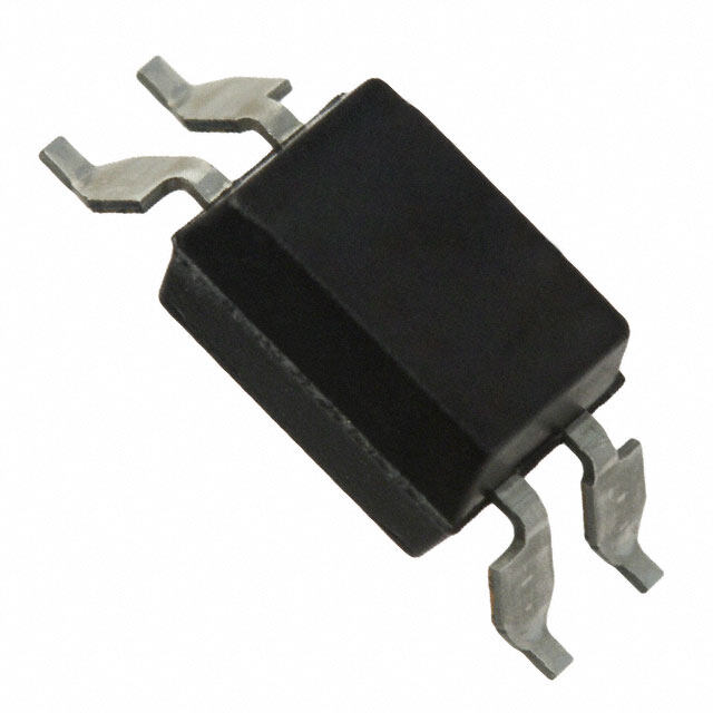
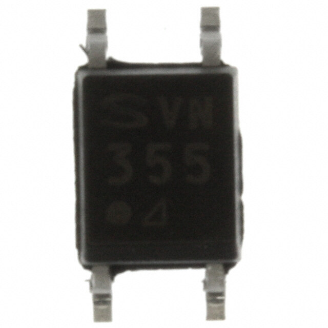
ICGOO电子元器件商城为您提供FOD2711AS由Fairchild Semiconductor设计生产,在icgoo商城现货销售,并且可以通过原厂、代理商等渠道进行代购。 FOD2711AS价格参考。Fairchild SemiconductorFOD2711AS封装/规格:光隔离器 - 晶体管,光电输出, 光隔离器 晶体管 输出 5000Vrms 1 通道 8-SMD。您可以下载FOD2711AS参考资料、Datasheet数据手册功能说明书,资料中有FOD2711AS 详细功能的应用电路图电压和使用方法及教程。
FOD2711AS是安森美(ON Semiconductor)生产的一款光隔离器,属于晶体管输出型光电耦合器。该器件主要由一个红外发光二极管和一个集成的光电晶体管组成,实现输入与输出之间的电气隔离。

其典型应用场景包括:工业自动化控制系统中的信号隔离,用于防止高电压或噪声干扰影响低压控制电路;开关电源和DC-DC转换器中,用于反馈回路的隔离,提高系统安全性和抗干扰能力;在电机驱动、PLC(可编程逻辑控制器)模块及工业通信接口中,实现数字信号的可靠传输;还可用于医疗设备中对患者连接部分进行电气隔离,确保使用安全;此外,在楼宇自动化、智能电表和家用电器(如变频空调)中也广泛应用,以增强系统的稳定性和安全性。

FOD2711AS具有高隔离电压、良好的共模抑制能力和稳定的工作性能,适用于需要高可靠性与长期稳定运行的环境。其紧凑的表面贴装封装也适合高密度PCB设计,便于现代电子设备的小型化和集成化需求。
| 参数 | 数值 |
| 产品目录 | |
| 描述 | OPTOISOLATOR 5KV TRANSISTOR 8SMD光隔离放大器 Isolated Error Amp Optocoupler |
| 产品分类 | |
| 品牌 | Fairchild Semiconductor |
| 产品手册 | |
| 产品图片 |
|
| rohs | 符合RoHS无铅 / 符合限制有害物质指令(RoHS)规范要求 |
| 产品系列 | 光耦合器/光电耦合器,光隔离放大器,Fairchild Semiconductor FOD2711AS- |
| 数据手册 | |
| 产品型号 | FOD2711AS |
| Vce饱和值(最大值) | 400mV |
| 上升/下降时间(典型值) | - |
| 产品种类 | 光隔离放大器 |
| 供应商器件封装 | 8-SMD |
| 包装 | 散装 |
| 单位重量 | 720 mg |
| 参考电压 | 1.24 V |
| 商标 | Fairchild Semiconductor |
| 安装类型 | 表面贴装 |
| 安装风格 | SMD/SMT |
| 封装 | Bulk |
| 封装/外壳 | 8-SMD(300 密耳)鸥翼型 |
| 封装/箱体 | MDIP-8 Gull Wing |
| 工作温度 | -40°C ~ 85°C |
| 工厂包装数量 | 1000 |
| 带宽 | 10 KHz |
| 打开/关闭时间(典型值) | - |
| 最大功率耗散 | 145 mW |
| 最大工作温度 | + 85 C |
| 最大正向二极管电压 | 1.5 V |
| 最大集电极/发射极电压 | 30 V |
| 最大集电极/发射极饱和电压 | 0.4 V |
| 最大集电极电流 | 50 mA |
| 最小工作温度 | - 40 C |
| 标准包装 | 1,000 |
| 正向电流 | 20 mA |
| 每芯片的通道数量 | 1 Channel |
| 电压-正向(Vf)(典型值) | 1.5V (最小值) |
| 电压-输出(最大值) | 30V |
| 电压-隔离 | 5000Vrms |
| 电流-DC正向(If) | - |
| 电流-输出/通道 | 50mA |
| 电流传输比(最大值) | 200% @ 10mA |
| 电流传输比(最小值) | 100% @ 10mA |
| 电流传递比 | 100 % to 200% |
| 系列 | FOD2711 |
| 绝缘电压 | 5000 Vrms |
| 输入类型 | DC |
| 输出类型 | 晶体管 |
| 输出设备 | Phototransistor |
| 通道数 | 1 |


.jpg)

.jpg)
PDF Datasheet 数据手册内容提取
Is Now Part of To learn more about ON Semiconductor, please visit our website at www.onsemi.com Please note: As part of the Fairchild Semiconductor integration, some of the Fairchild orderable part numbers will need to change in order to meet ON Semiconductor’s system requirements. Since the ON Semiconductor product management systems do not have the ability to manage part nomenclature that utilizes an underscore (_), the underscore (_) in the Fairchild part numbers will be changed to a dash (-). This document may contain device numbers with an underscore (_). Please check the ON Semiconductor website to verify the updated device numbers. The most current and up-to-date ordering information can be found at www.onsemi.com. Please email any questions regarding the system integration to Fairchild_questions@onsemi.com. ON Semiconductor and the ON Semiconductor logo are trademarks of Semiconductor Components Industries, LLC dba ON Semiconductor or its subsidiaries in the United States and/or other countries. ON Semiconductor owns the rights to a number of patents, trademarks, copyrights, trade secrets, and other intellectual property. A listing of ON Semiconductor’s product/patent coverage may be accessed at www.onsemi.com/site/pdf/Patent-Marking.pdf. ON Semiconductor reserves the right to make changes without further notice to any products herein. ON Semiconductor makes no warranty, representation or guarantee regarding the suitability of its products for any particular purpose, nor does ON Semiconductor assume any liability arising out of the application or use of any product or circuit, and specifically disclaims any and all liability, including without limitation special, consequential or incidental damages. Buyer is responsible for its products and applications using ON Semiconductor products, including compliance with all laws, regulations and safety requirements or standards, regardless of any support or applications information provided by ON Semiconductor. “Typical” parameters which may be provided in ON Semiconductor data sheets and/or specifications can and do vary in different applications and actual performance may vary over time. All operating parameters, including “Typicals” must be validated for each customer application by customer’s technical experts. ON Semiconductor does not convey any license under its patent rights nor the rights of others. ON Semiconductor products are not designed, intended, or authorized for use as a critical component in life support systems or any FDA Class 3 medical devices or medical devices with a same or similar classification in a foreign jurisdiction or any devices intended for implantation in the human body. Should Buyer purchase or use ON Semiconductor products for any such unintended or unauthorized application, Buyer shall indemnify and hold ON Semiconductor and its officers, employees, subsidiaries, affiliates, and distributors harmless against all claims, costs, damages, and expenses, and reasonable attorney fees arising out of, directly or indirectly, any claim of personal injury or death associated with such unintended or unauthorized use, even if such claim alleges that ON Semiconductor was negligent regarding the design or manufacture of the part. ON Semiconductor is an Equal Opportunity/Affirmative Action Employer. This literature is subject to all applicable copyright laws and is not for resale in any manner.
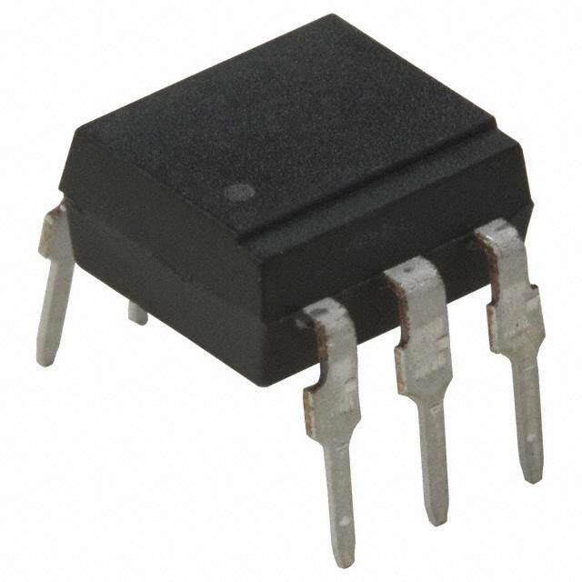
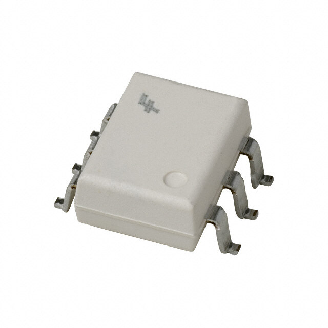
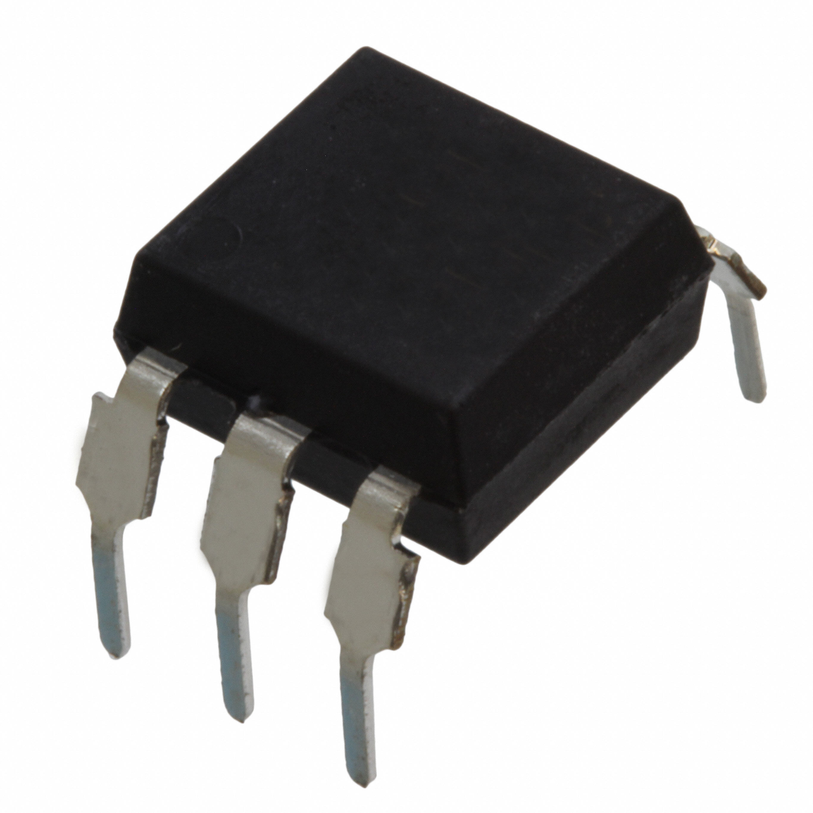
F O D 2 June 2010 7 1 1 A — FOD2711A O p Optically Isolated Error Amplifier t i c a l l Features Description y I s ■ Optocoupler, precision reference and error amplifier in The FOD2711A Optically Isolated Amplifier consists of o l single package the popular AZ431L precision programmable shunt ref- a t ■ 1.240V ± 1% reference erence and an optocoupler. The optocoupler is a gallium e d ■ CTR 100% to 200% arsenide (GaAs) light emitting diode optically coupled to E a silicon phototransistor. The reference voltage toler- r ■ 5,000V RMS isolation r ance is 1%. The current transfer ratio (CTR) ranges from o ■ UL approval E90700, Volume 2 100% to 200%. r A Applications It is primarily intended for use as the error amplifier/ m p reference voltage/optocoupler function in isolated AC to l ■ Power supplies regulation DC power supplies and dc/dc converters. ifi ■ DC to DC converters e When using the FOD2711A, power supply designers can r reduce the component count and save space in tightly packaged designs. The tight tolerance reference elimi- nates the need for adjustments in many applications. The device comes in a 8-pin dip white package. Functional Bock Diagram Package Outlines NC 1 8 LED 8 1 C 2 7 FB E 3 6 COMP 8 8 NC 4 5 GND 1 1 ©2010 Fairchild Semiconductor Corporation www.fairchildsemi.com FOD2711A Rev. 1.0.0
F O Pin Definitions D 2 7 Pin Number Pin Name Pin Description 1 1 1 NC Not connected A — 2 C Phototransistor Collector O 3 E Phototransistor Emitter p 4 NC Not connected ti c a 5 GND Ground l l y 6 COMP Error Amplifier Compensation. This pin is the output of the error amplifier.* I s 7 FB Voltage Feedback. This pin is the inverting input to the error amplifier o l a 8 LED Anode LED. This pin is the input to the light emitting diode. t e d *The compensation network must be attached between pins 6 and 7. E r r o Typical Application r A m p l i fi e r FAN4803 V1 PWM VO Control FOD2711A 2 8 6 R1 3 7 R2 5 ©2010 Fairchild Semiconductor Corporation www.fairchildsemi.com FOD2711A Rev. 1.0.0 2
F O Absolute Maximum Ratings (T = 25°C unless otherwise specified) D A 2 Stresses exceeding the absolute maximum ratings may damage the device. The device may not function or be 7 operable above the recommended operating conditions and stressing the parts to these levels is not recommended. 1 1 In addition, extended exposure to stresses above the recommended operating conditions may affect device reliability. A The absolute maximum ratings are stress ratings only. — O Symbol Parameter Value Units p t TSTG Storage Temperature -40 to +125 °C ic a TOPR Operating Temperature -40 to +85 °C ll y TSOL Lead Solder Temperature 260 for 10 sec. °C Is V Input Voltage 13.2 V o LED l a I Input DC Current 20 mA t LED e d VCEO Collector-Emitter Voltage 30 V E V Emitter-Collector Voltage 7 V r ECO r o I Collector Current 50 mA r C A PD1 Input Power Dissipation(1) 145 mW m PD2 Transistor Power Dissipation(2) 85 mW p l i PD3 Total Power Dissipation(3) 145 mW fi e r Notes: 1. Derate linearly from 25°C at a rate of 2.42mW/°C 2. Derate linearly from 25°C at a rate of 1.42mW/°C. 3. Derate linearly from 25°C at a rate of 2.42mW/°C. ©2010 Fairchild Semiconductor Corporation www.fairchildsemi.com FOD2711A Rev. 1.0.0 3
F O Electrical Characteristics (T = 25°C unless otherwise specified) D A 2 Input Characteristics 7 1 1 Symbol Parameter Test Conditions Min. Typ.* Max. Unit A — V LED Forward Voltage I = 10mA, V = V (Fig. 1) 1.5 V F LED COMP FB O VREF Reference Voltage VCOMP = VFB, ILED = 10mA (Fig.1) p t -40°C to +85°C 1.221 1.259 V ic a 25°C 1.228 1.240 1.252 ll y V Deviation of V Over T = -40 to +85°C 4 12 mV I REF (DEV) REF A s Temperature(4) o l a ∆V / Ratio of Vref Variation I = 10 mA, V = V to 12V -1.5 -2.7 mV/V t REF LED COMP REF e ∆V to the Output of the Error (Fig. 2) d COMP Amplifier E r I Feedback Input Current I = 10mA, R1 = 10kΩ (Fig. 3) 0.15 0.5 µA ro REF LED r I Deviation of I Over T = -40°C to +85°C 0.15 0.3 µA A REF (DEV) REF A Temperature(4) m p I Minimum Drive Current V = V (Fig. 1) 55 80 µA l LED (MIN) COMP FB i fi I Off-State Error Amplifier V = 6V, V = 0 (Fig. 4) 0.001 0.1 µA e (OFF) LED FB r Current | Z | Error Amplifier Output V = V , I = 0.1mA to 15mA, 0.25 Ω OUT COMP FB LED Impedance(5) f<1 kHZ) Output Characteristics Symbol Parameter Test Conditions Min. Typ. Max. Unit I Collector Dark Current V = 10V (Fig. 5) 50 nA CEO CE BV Emitter-Collector Voltage Breakdown I = 100µA 7 V ECO E BV Collector-Emitter Voltage Breakdown I = 1.0mA 70 V CEO C Transfer Characteristics Symbol Parameter Test Conditions Min. Typ. Max. Unit CTR Current Transfer Ratio I = 10mA, V = V , 100 200 % LED COMP FB V = 5V (Fig. 6) CE V Collector-Emitter Saturation I = 10mA, V = V 0.4 V CE(SAT) LED COMP FB, Voltage I = 2.5mA (Fig. 6) C Notes: 4. The deviation parameters V and I are defined as the differences between the maximum and REF(DEV) REF(DEV) minimum values obtained over the rated temperature range. The average full-range temperature coefficient of the reference input voltage, ∆V , is defined as: REF {V /V (T =25°C)}×106 ∆V (ppm/°C) = --------R----E---F---(--D----E----V---)--------R----E---F----------A--------------------------------------------- REF ∆T A where ∆T is the rated operating free-air temperature range of the device. A 5. The dynamic impedance is defined as |Z | = ∆V / ∆I . When the device is operating with two external OUT COMP LED resistors (see Figure 2), the total dynamic impedance of the circuit is given by: Z = ∆-----V---≈ Z × 1+R-----1--- OUT, TOT ∆I OUT R2 ©2010 Fairchild Semiconductor Corporation www.fairchildsemi.com FOD2711A Rev. 1.0.0 4
F O Electrical Characteristics (Continued) (T = 25°C unless otherwise specified) D A 2 7 Isolation Characteristics 1 1 Symbol Parameter Test Conditions Min. Typ. Max. Unit A — I Input-Output Insulation RH = 45%, T = 25°C, t = 5s, 1.0 µA I-O A Leakage Current V = 3000 VDC(6) O I-O p VISO Withstand Insulation RH ≤ 50%, TA = 25°C, t = 1 min.(6) 5000 Vrms tic Voltage a l R Resistance (Input to Output) V = 500 VDC(6) 1012 Ω ly I-O I-O I s o l a Switching Characteristics t e d Symbol Parameter Test Conditions Min. Typ. Max. Unit E r BW Bandwidth (Fig. 7) 10 kHZ ro r CMH Common Mode Transient ILED = 0mA, Vcm = 10 VPP, 1.0 kV/µs A Immunity at Output HIGH R = 2.2kΩ(7) (Fig. 8) m L CML Common Mode Transient I = 1mA, Vcm = 10 V 1.0 kV/µs p Immunity at Output LOW RLE D= 2.2kΩ(7) (Fig. 8) PP, lifi L e r Notes: 6. Device is considered as a two terminal device: Pins 1, 2, 3 and 4 are shorted together and Pins 5, 6, 7 and 8 are shorted together. 7. Common mode transient immunity at output high is the maximum tolerable (positive) dVcm/dt on the leading edge of the common mode impulse signal, Vcm, to assure that the output will remain high. Common mode transient immunity at output low is the maximum tolerable (negative) dVcm/dt on the trailing edge of the common pulse signal,Vcm, to assure that the output will remain low. ©2010 Fairchild Semiconductor Corporation www.fairchildsemi.com FOD2711A Rev. 1.0.0 5
F O Test Circuits D 2 7 I(LED) 1 I(LED) 1A 8 2 8 2 — VF O p 6 R1 6 3 3 ti c V V 7 7 al VCOMP ly VREF R2 VREF Is o 5 5 l a t e d Figure 1. VREF, VF, ILED (min.) Test Circuit Figure 2. ∆VREF / ∆VCOMP Test Circuit Er r o r A m p I(LED) I(OFF) li fi 8 2 8 2 e r IREF 6 6 3 3 V(LED) V 7 V 7 R1 5 5 Figure 3. IREF Test Circuit Figure 4. I(OFF) Test Circuit ICEO I(LED) IC 8 2 8 2 VCE VCE 6 6 3 3 7 V 7 VCOMP VREF 5 5 Figure 5. ICEO Test Circuit Figure 6. CTR, VCE(sat) Test Circuit ©2010 Fairchild Semiconductor Corporation www.fairchildsemi.com FOD2711A Rev. 1.0.0 6
F O Test Circuits (Continued) D 2 7 1 VCC = +5V DC 1 A IF = 10mA 47Ω — RL 1 8 O p 1µf ti c VOUT 2 7 a 0.1 VPP V0.I4N7V lly I s o 3 6 l a t e d E 4 5 r r o r A m Figure 7. Frequency Response Test Circuit p l i fi e r VCC = +5V DC IF = 0mA (A) IF = 10mA (B) R1 1 8 2.2kΩ VOUT 2 7 A B 3 6 4 5 VCM _ + 10VP-P Figure 8. CMH and CML Test Circuit ©2010 Fairchild Semiconductor Corporation www.fairchildsemi.com FOD2711A Rev. 1.0.0 7
F O Typical Performance Curves D 2 7 1 Fig. 9a LED Current vs. Cathode Voltage Fig. 9b LED Current vs. Cathode Voltage 1 A 15 150 — TVAC O=M 2P5 =°C V FB TVAC O= M 2P5=° CVFB O )A 10 mA) 100 p m( TNE 5 RENT ( 50 tica R R l RUC YL 0 PLY CU 0 ly Is P P o P U US – D -5 – SED -50 late I EL -10 IL-100 d E r -15 -150 r o -1.0 -0.5 0.0 0.5 1.0 1.5 -1 0 1 2 r VCOMP – CATHODE VOLTAGE (V) VCOMP – CATHODE VOLTAGE (V) A m p l i fi Fig. 10 Reference Voltage vs. Ambient Temperature Fig. 11 Reference Current vs. Ambient Temperature e r 280 1.244 ILED = 10mA AGE (V) 1.242 ILED = 10mA NT (nA) 224600 R1 = 10 kΩ T E E VOL 1.240 CURR 220 V – REFERENCREF 1111....222233332468 I – REFERENCE REF 111246800000 1.230 120 -40 -20 0 20 40 60 80 100 -40 -20 0 20 40 60 80 100 TA – AMBIENT TEMPERATURE (°C) TA – AMBIENT TEMPERATURE (°C) Fig. 12 Off-State Current vs. Ambient Temperature Fig. 13 Forward Current vs. Forward Voltage 20 1000 VCC = 13.2V NT (NA) 100 T (mA) 15 E N R E R R U R C U TE 10 D C 10 25°C TA AR 70°C 0°C S W F- R – OFOFF 1 I – FOF 5 I 0.1 -40 -20 0 20 40 60 80 100 0.9 1.0 1.1 1.2 1.3 1.4 TA – AMBIENT TEMPERATURE (°C) VF – FORWARD VOLTAGE (V) ©2010 Fairchild Semiconductor Corporation www.fairchildsemi.com FOD2711A Rev. 1.0.0 8
F O Typical Performance Curves (Continued) D 2 7 Fig. 14 Dark Current vs. Ambient Temperature Fig. 15 Collector Current vs. Ambient Temperature 1 1 10000 30 A VCE = 10V VCE = 5V — RRENT (nA) 1100000 URRENT (mA) 2205 ILED = 20mA Optica K CU OR C 15 ILED = 10mA lly I – DARCEO 110 C – COLLECT 150 ILED = 5mA Isolate I d 0.1 0 ILED = 1mA E -40 -20 0 20 40 60 80 100 0 10 20 30 40 50 60 70 80 90 100 r r TA – AMBIENT TEMPERATURE (°C) TA – AMBIENT TEMPERATURE (°C) or A m p Fig. 17 Saturation Voltage vs. Ambient Temperature Fig. 16 Current Transfer Ratio vs. LED Current l i fi 0.26 e O (%) 140 VCE = 5V GE (V) 0.24 r RATI 120 OLTA 0.22 R V NSFE 100 0°C TION 0.20 A A 0.18 R 25°C R T U RENT 80 70°C – SAT 0.16 UR AT) 0.14 F) – C 60 VCE(S 0.12 C/I (I 40 0.10 0 5 10 15 20 25 30 35 40 45 50 -40 -20 0 20 40 60 80 100 TA – AMBIENT TEMPERATURE (°C) ILED – FORWARD CURRENT (mA) Fig. 18 Collector Current vs. Collector Voltage Fig. 19 Rate of Change Vref to Vcomp vs. Temperature 35 T = 25°C -0.2 A V) A) 30 mV/ -0.4 NT (m 25 ILED = 20mA MP ( -0.6 E O R C UR 20 A V -0.8 C T OLLECTOR 1105 ILED = 10mA VREF / DEL --11..20 I – CC 5 ILED = 5mA DELTA -1.4 -1.6 I = 1mA LED 0 0 1 2 3 4 5 6 7 8 9 10 -60 -40 -20 0 20 40 60 80 100 120 VCE – COLLECTOR-EMITTER VOLTAGE (V) TEMPERATURE (°C) ©2010 Fairchild Semiconductor Corporation www.fairchildsemi.com FOD2711A Rev. 1.0.0 9
F O Typical Performance Curves (Continued) D 2 7 Fig. 20 Voltage Gain vs. Frequency 1 1 A VIFC =C 1=0 m10AV — 0 O N (dB) RL = 100Ω ptic AI a GE G -5 lly A LT Is VO o -10 l RL = 1kΩ a t e d -15 RL = 500Ω E 0.1 1 10 100 1000 r r FREQUENCY (kHZ) o r A m p l i fi e r ©2010 Fairchild Semiconductor Corporation www.fairchildsemi.com FOD2711A Rev. 1.0.0 10
F O The FOD2711A D 2 The FOD2711A is an optically isolated error amplifier. It Compensation 7 1 incorporates three of the most common elements neces- The compensation pin of the FOD2711A provides the 1 A sary to make an isolated power supply, a reference volt- opportunity for the designer to design the frequency age, an error amplifier, and an optocoupler. It is — response of the converter. A compensation network may functionally equivalent to the popular AZ431L shunt volt- be placed between the COMP pin and the FB pin. In O age regulator plus the CNY17F-3 optocoupler. typical low-bandwidth systems, a 0.1µF capacitor may p t Powering the Secondary Side be used. For converters with more stringent require- ic a ments, a network should be designed based on mea- l The LED pin in the FOD2711A powers the secondary l surements of the system’s loop. An excellent reference y side, and in particular provides the current to run the for this process may be found in “Practical Design of Is LED. The actual structure of the FOD2711A dictates the o Power Supplies” by Ron Lenk, IEEE Press, 1998. minimum voltage that can be applied to the LED pin: The la t error amplifier output has a minimum of the reference Secondary Ground e d voltage, and the LED is in series with that. Minimum volt- The GND pin should be connected to the secondary E age applied to the LED pin is thus 1.24V + 1.5V = 2.74V. ground of the converter. r This voltage can be generated either directly from the ro output of the converter, or else from a slaved secondary No Connect Pins r A winding. The secondary winding will not affect regula- The NC pins have no internal connection. They should m tion, as the input to the FB pin may still be taken from the not have any connection to the secondary side, as this p output winding. may compromise the isolation structure. li fi The LED pin needs to be fed through a current limiting Photo-Transistor er resistor. The value of the resistor sets the amount of cur- The Photo-transistor is the output of the FOD2711A. In a rent through the LED, and thus must be carefully normal configuration the collector will be attached to a selected in conjunction with the selection of the primary pull-up resistor and the emitter grounded. There is no side resistor. base connection necessary. Feedback The value of the pull-up resistor, and the current limiting Output voltage of a converter is determined by selecting resistor feeding the LED, must be carefully selected to a resistor divider from the regulated output to the FB pin. account for voltage range accepted by the PWM IC, and The FOD2711A attempts to regulate its FB pin to the for the variation in current transfer ratio (CTR) of the reference voltage, 1.24V. The ratio of the two resistors opto-isolator itself. should thus be: Example: The voltage feeding the LED pins is +12V, the R V voltage feeding the collector pull-up is +10V, and the -----------T---O----P-------- = -----O----U---T--–1 PWM IC is the Fairchild KA1H0680, which has a 5V ref- R V BOTTOM REF erence. If we select a 10KΩ resistor for the LED, the The absolute value of the top resistor is set by the input maximum current the LED can see is: offset current of 0.8µA. To achieve 1% accuracy, the (12V–2.74V) / 10kΩ = 926µA. resistance of R should be: TOP The CTR of the opto-isolator is a minimum of 100%, and V –1.24 -----O----U---T-------------------->80µA so the minimum collector current of the photo-transistor R when the diode is full on is also 926µA. The collector TOP resistor must thus be such that: ------1---0----V------–----5----V--------<926µA or R >5.4KΩ; R COLLECTOR COLLECTOR select 10kΩ to allow some margin. ©2010 Fairchild Semiconductor Corporation www.fairchildsemi.com FOD2711A Rev. 1.0.0 11
F O Ordering Information D 2 7 Option Example Part Number Description 1 1 No Option FOD2711A Standard Through Hole A S FOD2711AS Surface Mount Lead Bend — SD FOD2711ASD Surface Mount; Tape and Reel O p T FOD2711AT 0.4" Lead Spacing t i c V FOD2711AV VDE0884 a l l y TV FOD2711ATV VDE0884; 0.4” Lead Spacing I s SV FOD2711ASV VDE0884; Surface Mount o l a SDV FOD2711ASDV VDE0884; Surface Mount; Tape and Reel t e d E r r o r A Marking Information m p l i fi e r 1 2711A 2 V XX YY B 6 3 4 5 Definitions 1 Fairchild logo 2 Device number 3 VDE mark (Note: Only appears on parts ordered with VDE option – See order entry table) 4 Two digit year code, e.g., ‘03’ 5 Two digit work week ranging from ‘01’ to ‘53’ 6 Assembly package code ©2010 Fairchild Semiconductor Corporation www.fairchildsemi.com FOD2711A Rev. 1.0.0 12
F O Carrier Tape Specifications D 2 7 D 1 0 1 P P A 0 2 t E K — 0 O p t i c F a W1 B0 A0 W lly I s o l a t e d P UserDirectionofFeed E d D 1 r r o r A Symbol Description Dimension in mm m p W Tape Width 16.0 ± 0.3 l i fi t Tape Thickness 0.30 ± 0.05 e r P Sprocket Hole Pitch 4.0 ± 0.1 0 D Sprocket Hole Diameter 1.55 ± 0.05 0 E Sprocket Hole Location 1.75 ± 0.10 F Pocket Location 7.5 ± 0.1 P 4.0 ± 0.1 2 P Pocket Pitch 12.0 ± 0.1 A Pocket Dimensions 10.30 ±0.20 0 B 10.30 ±0.20 0 K 4.90 ±0.20 0 W Cover Tape Width 1.6 ± 0.1 1 d Cover Tape Thickness 0.1 max Max. Component Rotation or Tilt 10° R Min. Bending Radius 30 Reflow Profile 245 C, 10–30 s 300 250 260 C peak C) e (° 200 r u 150 at per 100 Time above 183 C, <160 sec m Te 50 Ramp up = 2–1 0C/sec 0 0 0.5 1 1.5 2 2.5 3 3.5 4 4.5 Time (Minute) • Peak reflow temperature: 2 60C (package surface temperature) • Time of temperature higher than 1 83C for 160 seconds or less • One time soldering reflow is recommended ©2010 Fairchild Semiconductor Corporation www.fairchildsemi.com FOD2711A Rev. 1.0.0 13
None
None
None
ON Semiconductor and are trademarks of Semiconductor Components Industries, LLC dba ON Semiconductor or its subsidiaries in the United States and/or other countries. ON Semiconductor owns the rights to a number of patents, trademarks, copyrights, trade secrets, and other intellectual property. A listing of ON Semiconductor’s product/patent coverage may be accessed at www.onsemi.com/site/pdf/Patent−Marking.pdf. ON Semiconductor reserves the right to make changes without further notice to any products herein. ON Semiconductor makes no warranty, representation or guarantee regarding the suitability of its products for any particular purpose, nor does ON Semiconductor assume any liability arising out of the application or use of any product or circuit, and specifically disclaims any and all liability, including without limitation special, consequential or incidental damages. Buyer is responsible for its products and applications using ON Semiconductor products, including compliance with all laws, regulations and safety requirements or standards, regardless of any support or applications information provided by ON Semiconductor. “Typical” parameters which may be provided in ON Semiconductor data sheets and/or specifications can and do vary in different applications and actual performance may vary over time. All operating parameters, including “Typicals” must be validated for each customer application by customer’s technical experts. ON Semiconductor does not convey any license under its patent rights nor the rights of others. ON Semiconductor products are not designed, intended, or authorized for use as a critical component in life support systems or any FDA Class 3 medical devices or medical devices with a same or similar classification in a foreign jurisdiction or any devices intended for implantation in the human body. Should Buyer purchase or use ON Semiconductor products for any such unintended or unauthorized application, Buyer shall indemnify and hold ON Semiconductor and its officers, employees, subsidiaries, affiliates, and distributors harmless against all claims, costs, damages, and expenses, and reasonable attorney fees arising out of, directly or indirectly, any claim of personal injury or death associated with such unintended or unauthorized use, even if such claim alleges that ON Semiconductor was negligent regarding the design or manufacture of the part. ON Semiconductor is an Equal Opportunity/Affirmative Action Employer. This literature is subject to all applicable copyright laws and is not for resale in any manner. PUBLICATION ORDERING INFORMATION LITERATURE FULFILLMENT: N. American Technical Support: 800−282−9855 Toll Free ON Semiconductor Website: www.onsemi.com Literature Distribution Center for ON Semiconductor USA/Canada 19521 E. 32nd Pkwy, Aurora, Colorado 80011 USA Europe, Middle East and Africa Technical Support: Order Literature: http://www.onsemi.com/orderlit Phone: 303−675−2175 or 800−344−3860 Toll Free USA/Canada Phone: 421 33 790 2910 Fax: 303−675−2176 or 800−344−3867 Toll Free USA/Canada Japan Customer Focus Center For additional information, please contact your local Email: orderlit@onsemi.com Phone: 81−3−5817−1050 Sales Representative © Semiconductor Components Industries, LLC www.onsemi.com www.onsemi.com 1
Mouser Electronics Authorized Distributor Click to View Pricing, Inventory, Delivery & Lifecycle Information: O N Semiconductor: FOD2711AV FOD2711ASD FOD2711AS FOD2711A FOD2711ASDV FOD2711ASV FOD2711ATV