ICGOO在线商城 > 集成电路(IC) > PMIC - 照明,镇流器控制器 > FL7930BMX
 Datasheet下载
- 型号: FL7930BMX
- 制造商: Fairchild Semiconductor
- 库位|库存: xxxx|xxxx
- 要求:
| 数量阶梯 | 香港交货 | 国内含税 |
| +xxxx | $xxxx | ¥xxxx |
查看当月历史价格
查看今年历史价格
FL7930BMX产品简介:
ICGOO电子元器件商城为您提供FL7930BMX由Fairchild Semiconductor设计生产,在icgoo商城现货销售,并且可以通过原厂、代理商等渠道进行代购。 FL7930BMX价格参考。Fairchild SemiconductorFL7930BMX封装/规格:PMIC - 照明,镇流器控制器, 。您可以下载FL7930BMX参考资料、Datasheet数据手册功能说明书,资料中有FL7930BMX 详细功能的应用电路图电压和使用方法及教程。
FL7930BMX 是安森美半导体(ON Semiconductor)推出的一款专用于照明的电源管理集成电路(PMIC),具体属于镇流器控制器类别。它主要应用于荧光灯照明系统,尤其是冷阴极荧光灯(CCFL)背光系统,如液晶显示器(LCD)电视、显示器和笔记本电脑的背光驱动。

该芯片采用固定频率的电流模式控制架构,具备良好的稳定性和响应速度,支持宽输入电压范围,适合用于升压(Boost)拓扑结构中,将低压直流电源升压为高压交流信号以驱动CCFL灯管。

FL7930BMX具备多种保护功能,如过电流保护(OCP)、灯管开路保护和欠压锁定(UVLO),提高了系统的可靠性和安全性。同时,它还支持调光功能,可通过外部信号调节灯管亮度,满足不同应用场景下的照明需求。

综上,FL7930BMX 主要应用于需要高效、稳定背光驱动的CCFL照明系统,尤其适合LCD背光、工业照明及特种照明设备。
| 参数 | 数值 |
| 产品目录 | 集成电路 (IC)半导体 |
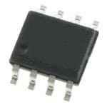
| 描述 | IC PFC CTLR FLYBACK/BOUND 8SOIC功率因数校正 - PFC PFC Controller for Lighting; 2nd OVP |
| 产品分类 | |
| 品牌 | Fairchild Semiconductor |
| 产品手册 | |
| 产品图片 |
|
| rohs | 符合RoHS无铅 / 符合限制有害物质指令(RoHS)规范要求 |
| 产品系列 | 电源管理 IC,功率因数校正 - PFC,Fairchild Semiconductor FL7930BMX- |
| 数据手册 | |
| 产品型号 | FL7930BMX |
| PCN组件/产地 | |
| 产品种类 | 功率因数校正 - PFC |
| 供应商器件封装 | 8-SOP |
| 其它名称 | FL7930BMXDKR |
| 制造商卷带宽度 | 12mm |
| 制造商卷带材料 | 塑料 |
| 制造商卷带直径 | 13"(330mm) |
| 包装 | Digi-Reel® |
| 单位重量 | 143 mg |
| 商标 | Fairchild Semiconductor |
| 图号 | 261; MKT-M08A; ; 8 |
| 安装类型 | 表面贴装 |
| 安装风格 | SMD/SMT |
| 封装 | Reel |
| 封装/外壳 | 8-SOIC(0.154",3.90mm 宽) |
| 封装/箱体 | SOIC-8 |
| 工作温度 | -40°C ~ 125°C |
| 工厂包装数量 | 2500 |
| 开关频率 | 300 kHz |
| 最大工作温度 | + 125 C |
| 最小工作温度 | - 40 C |
| 标准包装 | 1 |
| 特色产品 | http://www.digikey.cn/product-highlights/cn/zh/fairchild-semiconductor-led-solutions/3901 |
| 电压-电源 | 13 V ~ 20 V |
| 电流-灌/拉输出 | - |
| 电流-电源 | 2.5mA |
| 类型 | 镇流器控制器 |
| 系列 | FL7930 |
| 调光 | 无 |
| 频率 | 250kHz ~ 350kHz |


- 商务部:美国ITC正式对集成电路等产品启动337调查
- 曝三星4nm工艺存在良率问题 高通将骁龙8 Gen1或转产台积电
- 太阳诱电将投资9.5亿元在常州建新厂生产MLCC 预计2023年完工
- 英特尔发布欧洲新工厂建设计划 深化IDM 2.0 战略
- 台积电先进制程称霸业界 有大客户加持明年业绩稳了
- 达到5530亿美元!SIA预计今年全球半导体销售额将创下新高
- 英特尔拟将自动驾驶子公司Mobileye上市 估值或超500亿美元
- 三星加码芯片和SET,合并消费电子和移动部门,撤换高东真等 CEO
- 三星电子宣布重大人事变动 还合并消费电子和移动部门
- 海关总署:前11个月进口集成电路产品价值2.52万亿元 增长14.8%


PDF Datasheet 数据手册内容提取
Is Now Part of To learn more about ON Semiconductor, please visit our website at www.onsemi.com Please note: As part of the Fairchild Semiconductor integration, some of the Fairchild orderable part numbers will need to change in order to meet ON Semiconductor’s system requirements. Since the ON Semiconductor product management systems do not have the ability to manage part nomenclature that utilizes an underscore (_), the underscore (_) in the Fairchild part numbers will be changed to a dash (-). This document may contain device numbers with an underscore (_). Please check the ON Semiconductor website to verify the updated device numbers. The most current and up-to-date ordering information can be found at www.onsemi.com. Please email any questions regarding the system integration to Fairchild_questions@onsemi.com. ON Semiconductor and the ON Semiconductor logo are trademarks of Semiconductor Components Industries, LLC dba ON Semiconductor or its subsidiaries in the United States and/or other countries. ON Semiconductor owns the rights to a number of patents, trademarks, copyrights, trade secrets, and other intellectual property. A listing of ON Semiconductor’s product/patent coverage may be accessed at www.onsemi.com/site/pdf/Patent-Marking.pdf. ON Semiconductor reserves the right to make changes without further notice to any products herein. ON Semiconductor makes no warranty, representation or guarantee regarding the suitability of its products for any particular purpose, nor does ON Semiconductor assume any liability arising out of the application or use of any product or circuit, and specifically disclaims any and all liability, including without limitation special, consequential or incidental damages. Buyer is responsible for its products and applications using ON Semiconductor products, including compliance with all laws, regulations and safety requirements or standards, regardless of any support or applications information provided by ON Semiconductor. “Typical” parameters which may be provided in ON Semiconductor data sheets and/or specifications can and do vary in different applications and actual performance may vary over time. All operating parameters, including “Typicals” must be validated for each customer application by customer’s technical experts. ON Semiconductor does not convey any license under its patent rights nor the rights of others. ON Semiconductor products are not designed, intended, or authorized for use as a critical component in life support systems or any FDA Class 3 medical devices or medical devices with a same or similar classification in a foreign jurisdiction or any devices intended for implantation in the human body. Should Buyer purchase or use ON Semiconductor products for any such unintended or unauthorized application, Buyer shall indemnify and hold ON Semiconductor and its officers, employees, subsidiaries, affiliates, and distributors harmless against all claims, costs, damages, and expenses, and reasonable attorney fees arising out of, directly or indirectly, any claim of personal injury or death associated with such unintended or unauthorized use, even if such claim alleges that ON Semiconductor was negligent regarding the design or manufacture of the part. ON Semiconductor is an Equal Opportunity/Affirmative Action Employer. This literature is subject to all applicable copyright laws and is not for resale in any manner.
F L 7 9 3 0 October 2013 B — S i n g FL7930B le - S Single-Stage Flyback and Boundary-Mode PFC ta g e Controller for Lighting F l y b a c k Features Description a n Additional OVP Detection Pin The FL7930B is an active power factor correction d (PFC) controller for boost PFC applications that B VIN-Absent Detection operate in critical conduction mode (CRM). It uses a ou Maximum Switching Frequency Limitation voltage-mode PWM that compares an internal ramp n signal with the error amplifier output to generate a d Internal Soft-Start and Startup without Overshoot MOSFET turn-off signal. Because the voltage-mode ar y CRM PFC controller does not need rectified AC line Internal Total Harmonic Distortion (THD) Optimizer voltage information, it saves the power loss of an input -M Precise Adjustable Output Over-Voltage Protection voltage sensing network necessary for a current-mode o d Open-Feedback Protection and Disable Function CRM PFC controller. e P Zero Current Detector (ZCD) FL7930B provides over-voltage protection (OVP), open- F feedback protection, over-current protection (OCP), C 150 μs Internal Startup Timer input-voltage-absent detection, and under-voltage C lockout protection (UVLO). The additional OVP pin can o MOSFET Over-Current Protection (OCP) n be used to shut down the boost power stage when t Under-Voltage Lockout with 3.5 V Hysteresis output voltage exceeds OVP level due to the resistors ro Low Startup and Operating Current that are connected at INV pin are damaged. The lle FL7930B can be disabled if the INV pin voltage is lower r Totem-Pole Output with High State Clamp than 0.45 V and the operating current decreases to a fo very low level. Using a new variable on-time control r +500/-800 mA Peak Gate Drive Current method, total harmonic distortion (THD) is lower than in L i 8-Pin, Small-Outline Package (SOP) conventional CRM boost PFC ICs. g h ti n Applications g Ballast General LED Lighting Industrial, Commercial, and Residential Fixtures Outdoor Lighting: Street, Roadway, Parking, Construction, Ornamental LED Lighting Fixtures Ordering Information Operating Packing Part Number Top Mark Package Temperature Range Method FL7930BMX_G -40 to +125°C FL7930BG 8-Lead Small Outline Package (SOP) Tape & Reel © 2010 Fairchild Semiconductor Corporation www.fairchildsemi.com FL7930B • Rev. 1.0.4
F L 7 Application Diagram 9 3 0 DC OUTPUT B — S i n g l e - S t a Vcc g FL7930B e Line Filter 8 VCC Out 74 Fly 5 CS b AC INPUT ZCD 1 a 3 INV c COMP 2 k GNDOVP a 6 n d B o u n d Figure 1. Typical Boost PFC Application a r y - M o d e P F C FL7930B C 1 INV VCC 8 o n CF1 CF2 CHF 2 OVP GATE 7 tr o 3 COMP GND 6 l l e 4 CS ZCD 5 r f o r L i g h t i Figure 2. Typical Application of Single-Stage Flyback Converter n g © 2010 Fairchild Semiconductor Corporation www.fairchildsemi.com FL7930B • Rev. 1.0.4 2
F L 7 Internal Block Diagram 9 3 0 B VCC H:open — VREF 2.5VREF 8 VCC VCC VBIAS InBteiarnsal reset - VZ Sin + mp uit VTH(S/S) gl ClaCirc 8.5 12 e-S ZCD 5 - t VCC a VTH(ZCD) + RTemstearrt DGraivteer 7 OUT ge F fMAX l Limit VO(MAX) y b OpTtiHmDiz ed S Q a Sawtooth Control Range + c Generator Compensation - R Q k a n d Overshoot-less 40kW Control + 4 CS B 8pF - o u INV 1 - VCS_LIM n VREF SSVttReaEpiFr + 6 GND da r Clamp y Circuit - reset M VIN Absent o COMP 3 d e disable P disable Thermal F Shutdown - C VREF 0.35 0.45 2.5 2.675 C + OVP 2 INV_oOpeVnP VOVP,LH + disable on t r - 2.5 2.88 ol le Figure 3. Functional Block Diagram r f o r L i g h t i n g © 2010 Fairchild Semiconductor Corporation www.fairchildsemi.com FL7930B • Rev. 1.0.4 3
F L 7 Pin Configuration 9 3 0 B V OUT GND ZCD CC — S i n g l e FL7930BG - S t 8-SOP a g e F l y b a c INV OVP COMP CS k a Figure 4. Pin Configuration (Top View) n d B o u n Pin Definitions d a r y Pin # Name Description - M This pin is the inverting input of the error amplifier. The output voltage of the boost PFC converter o 1 INV d should be resistively divided to 2.5 V. e 2 OVP This pin is used to detect PFC output over voltage when INV pin information is not correct. P F This pin is the output of the transconductance error amplifier. Components for the output voltage C 3 COMP compensation should be connected between this pin and GND. C o This pin is the input of the over-current protection comparator. The MOSFET current is sensed n 4 CS using a sensing resistor and the resulting voltage is applied to this pin. An internal RC filter is tr o included to filter switching noise. l l e This pin is the input of the zero-current detection (ZCD) block. If the voltage of this pin goes r 5 ZCD higher than 1.5 V, then goes lower than 1.4 V, the MOSFET is turned on. f o r This pin is used for the ground potential of all the pins. For proper operation, the signal ground 6 GND L and the power ground should be separated. i g h This pin is the gate drive output. The peak sourcing and sinking current levels are +500 mA and t 7 OUT -800 mA, respectively. For proper operation, the stray inductance in the gate driving path must be in minimized. g 8 V This is the IC supply pin. IC current and MOSFET drive current are supplied using this pin. CC © 2010 Fairchild Semiconductor Corporation www.fairchildsemi.com FL7930B • Rev. 1.0.4 4
F L 7 Absolute Maximum Ratings 9 3 0 Stresses exceeding the absolute maximum ratings may damage the device. The device may not function or be B operable above the recommended operating conditions and stressing the parts to these levels is not recommended. — In addition, extended exposure to stresses above the recommended operating conditions may affect device reliability. S The absolute maximum ratings are stress ratings only. i n g Symbol Parameter Min. Max. Unit l e - V Supply Voltage V V S CC Z t a I , I Peak Drive Output Current -800 +500 mA OH OL g e ICLAMP Driver Output Clamping Diodes VO>VCC or VO<-0.3 V -10 +10 mA F IDET Detector Clamping Diodes -10 +10 mA ly b Error Amplifier Input, Output, OVP Input, ZCD, RDY, and OVP Pins(1) -0.3 8.0 a V V c IN CS Input Voltage(2) -10.0 6.0 k a TJ Operating Junction Temperature +150 °C n d TA Operating Temperature Range -40 +125 °C B T Storage Temperature Range -65 +150 °C o STG u ESD Electrostatic Discharge Human Body Model, JESD22-A114 2.5 kV nd Capability Charged Device Model, JESD22-C101 2.0 a r y Notes: - M 1. When this pin is supplied by external power sources by accident, its maximum allowable current is 50 mA. o 2. In case of DC input, the acceptable input range is -0.3 V~6 V: within 100 ns -10 V~6 V is acceptable, but d electrical specifications are not guaranteed during such a short time. e P F C C o Thermal Impedance n t r o Symbol Parameter Min. Max. Unit l l e Thermal Resistance, Junction-to-Ambient(3) 150 °C/W r JA f o Note: r 3. Regarding the test environment and PCB type, please refer to JESD51-2 and JESD51-10. L ig h t i n g © 2010 Fairchild Semiconductor Corporation www.fairchildsemi.com FL7930B • Rev. 1.0.4 5
F L 7 Electrical Characteristics 9 3 0 V = 14 V and T = -40°C~+125°C, unless otherwise specified. B CC A — Symbol Parameter Conditions Min. Typ. Max. Unit S VCC Section in g V Start Threshold Voltage V Increasing 11 12 13 V l START CC e - V Stop Threshold Voltage V Decreasing 7.5 8.5 9.5 V S STOP CC t a HYUVLO UVLO Hysteresis 3.0 3.5 4.0 V g e VZ Zener Voltage ICC=20 mA 20 22 24 V F VOP Recommended Operating Range 13 20 V ly b Supply Current Section a c I Startup Supply Current V =V -0.2 V 120 190 µA k START CC START a IOP Operating Supply Current Output Not Switching 1.5 3.0 mA n d I Dynamic Operating Supply Current 50 kHz, C=1 nF 2.5 4.0 mA DOP I B I Operating Current at Disable V =0 V 90 160 230 µA o OPDIS INV u Error Amplifier Section n d a V Voltage Feedback Input Threshold1 T =25°C 2.465 2.500 2.535 V REF1 A r y VREF1 Line Regulation VCC=14 V~20 V 0.1 10.0 mV -M VREF2 Temperature Stability of VREF1(4) 20 mV od e I Input Bias Current V =1 V~4 V -0.5 0.5 µA EA,BS INV P I Output Source Current V =V -0.1 V -12 µA F EAS,SR INV REF C IEAS,SK Output Sink Current VINV=VREF +0.1 V 12 µA C o V Output Upper Clamp Voltage V =1 V, V =0 V 6.0 6.5 7.0 V n EAH INV CS t r V Zero Duty Cycle Output Voltage 0.9 1.0 1.1 V o EAZ l l gm Transconductance(4) 90 115 140 µmho er f Maximum On-Time Section o r t Maximum On-Time Programming 1 T =25°C, V =1 V 35.5 41.5 47.5 µs L ON,MAX1 A ZCD i g tON,MAX2 Maximum On-Time Programming 2 TIZAC=D2=50°.4C6, 9 mA 11.2 13.0 14.8 µs htin g Current-Sense Section Current Sense Input Threshold V 0.7 0.8 0.9 V CS Voltage Limit I Input Bias Current V =0~1 V -1.0 -0.1 1.0 µA CS,BS CS t Current Sense Delay to Output(4) dV/dt=1 V/100 ns, 350 500 ns CS,D from 0 V to 5 V Continued on the following page… © 2010 Fairchild Semiconductor Corporation www.fairchildsemi.com FL7930B • Rev. 1.0.4 6
F L 7 Electrical Characteristics 9 3 0 VCC = 14 V and TA = -40°C~+125°C, unless otherwise specified. B — Symbol Parameter Conditions Min. Typ. Max. Unit S Zero-Current Detect Section i n VZCD Input Voltage Threshold(4) 1.35 1.50 1.65 V gle HYZCD Detect Hysteresis(4) 0.05 0.10 0.15 V -S t V Input High Clamp Voltage I =3 mA 5.5 6.2 7.5 V a CLAMPH DET g V Input Low Clamp Voltage I =-3 mA 0 0.65 1.00 V e CLAMPL DET F IZCD,BS Input Bias Current VZCD=1 V~5 V -1.0 -0.1 1.0 µA ly IZCD,SR Source Current Capability(4) TA=25°C -4 mA ba IZCD,SK Sink Current Capability(4) TA=25°C 10 mA ck a Maximum Delay From ZCD to Output dV/dt=-1 V/100 ns, from tZCD,D Turn-On(4) 5 V to 0 V 100 200 ns nd B Output Section o u VOH Output Voltage High IO=-100 mA, TA=25°C 9.2 11.0 12.8 V n d VOL Output Voltage Low IO=200 mA, TA=25°C 1.0 2.5 V a r t Rising Time(4) C =1 nF 50 100 ns y RISE IN - M t Falling Time(4) C =1 nF 50 100 ns FALL IN o V Maximum Output Voltage V =20 V, I =100 µA 11.5 13.0 14.5 V d O,MAX CC O e V Output Voltage with UVLO Activated V =5 V, I =100 µA 1 V P O,UVLO CC O F Restart / Maximum Switching Frequency Limit Section C C t Restart Timer Delay 50 150 300 µs RST o f Maximum Switching Frequency(4) 250 300 350 kHz n MAX t r Soft-Start Timer Section o l l e tSS Internal Soft-Soft(4) 3 5 7 ms r f Protections o r V OVP Threshold Voltage at INV Pin T =25°C 2.620 2.675 2.730 V L OVP,INV A i g HY OVP Hysteresis at INV Pin T =25°C 0.120 0.175 0.230 V h OVP,INV A t i V OVP Threshold Voltage at OVP Pin T =25°C 2.740 2.845 2.960 V n OVP,OVP A g HY OVP Hysteresis at OVP Pin T =25°C 0.345 V OVP,OVP A V Enable Threshold Voltage 0.40 0.45 0.50 V EN HY Enable Hysteresis 0.05 0.10 0.15 V EN T Thermal Shutdown Temperature(4) 125 140 155 °C SD T Hysteresis Temperature of TSD(4) 60 °C HYS Note: 4. These parameters, although guaranteed by design, are not production tested. © 2010 Fairchild Semiconductor Corporation www.fairchildsemi.com FL7930B • Rev. 1.0.4 7
F L 7 Comparison of FL6961 and FL7930B 9 3 0 B Function FL6961 FL7930B FL7930B Advantages — No External Circuit for additional OVP S OVP Pin None Integrated Reduction of Power Loss and BOM Cost Caused by in Additional OVP Circuit g l e Abnormal CCM Operation Prohibited -S Frequency Limit None Integrated Abnormal Inductor Current Accumulation Can Be ta g Prohibited e Increase System Reliability by Testing for Input Supply F l y Voltage b VIN-Absent Detection None Integrated Guarantee Stable Operation at Short Electric Power ac Failure k a Soft-Start and Reduce Voltage and Current Stress at Startup nd Startup without None Integrated Eliminate Audible Noise Due to Unwanted OVP B Overshoot Triggering o u Can Avoid Burst Operation at Light Load and High Input n d Control Range Voltage a None Integrated r Compensation Reduce Probability of Audible Noise Due to Burst y - Operation M o THD Optimizer External Internal No External Resistor is Needed d e 140°C with Stable and Reliable TSD Operation P TSD None F 60°C Hysteresis Converter Temperature Range Limited Range C C Control Range None Integrated o Compensation n t r o ll e r f Comparison of FL7930B and FL7930C o r L Function FL7930B FL7930C FL7930B Remark ig h RDY Pin None Integrated User Choice for the Use of Number #2 Pin tin OVP Pin Integrated None g © 2010 Fairchild Semiconductor Corporation www.fairchildsemi.com FL7930B • Rev. 1.0.4 8
F L 7 Typical Performance Characteristics 9 3 0 B — S i n g l e - S t a g e F l y b a c k a n Figure 5. Voltage Feedback Input Threshold 1 Figure 6. Start Threshold Voltage (VSTART) vs. TA d (VREF1) vs. TA B o u n d a r y - M o d e P F C C o n t r o l l er Figure 7. Stop Threshold Voltage (VSTOP) vs. TA Figure 8. Startup Supply Current (ISTART) vs. TA fo r L i g h t i n g Figure 9. Operating Supply Current (I ) vs. T Figure 10. Output Upper Clamp Voltage (V ) vs. T OP A EAH A © 2010 Fairchild Semiconductor Corporation www.fairchildsemi.com FL7930B • Rev. 1.0.4 9
F L 7 Typical Performance Characteristics 9 3 0 B — S i n g l e - S t a g e F l y b a c k a n Figure 11. Zero Duty Cycle Output Voltage (V ) Figure 12. Maximum On-Time Program 1 (t ) d EAZ ON,MAX1 vs. T vs. T B A A o u n d a r y - M o d e P F C C o n t r o l l e r Figure 13. Maximum On-Time Program 2 (tON,MAX2) Figure 14. Current-Sense Input Threshold Voltage fo vs. T Limit (V ) vs. T r A CS A L i g h t i n g Figure 15. Input High Clamp Voltage (V ) CLAMPH Figure 16. Input Low Clamp Voltage (V ) vs. T vs. T CLAMPL A A © 2010 Fairchild Semiconductor Corporation www.fairchildsemi.com FL7930B • Rev. 1.0.4 10
F L 7 Typical Performance Characteristics 9 3 0 B — S i n g l e - S t a g e F l y b a c k a n Figure 17. Output Voltage High (VOH) vs. TA Figure 18. Output Voltage Low (VOL) vs. TA d B o u n d a r y - M o d e P F C C o n t r o l l e r Figure 19. Restart Timer Delay (tRST) vs. TA Figure 20. OVP Threshold at OVP Pin (VOVP,OVP) fo vs. TA r L i g h t i n g Figure 21. Output Saturation Voltage (V ) Figure 22. OVP Threshold Voltage (V ) vs. T RDY,SAT OVP A vs. T A © 2010 Fairchild Semiconductor Corporation www.fairchildsemi.com FL7930B • Rev. 1.0.4 11
F L 7 Applications Information 9 3 0 1. Startup: Normally, supply voltage (VCC) of a PFC VOUTPFC B block is fed from the additional power supply, which can - 2.885V — be called standby power. Without this standby power, 2nd OVP high + S auxiliary winding for zero current detection can be used abslo cak s uepxcpelye sdosu 1rc2e V. ,O inncteer nthael osuppepralyti ovno ltiasg een oafb tlheed PuFntCil 2.885 OVP ddiissaabbllee2.52.675 +- 2.675V/2.5V 2OVP ingle tchuer revnotl tiasg sei ndkrinogp sfr otom 8V.5 V. . If VCC exceeds VZ, 20 mA INV Open 0.350.45 - -S CC + 0.45V/0.35V ta PFC Inductor + 2.5V g VINPFC VOUTPFC INV e - 1 F Aux. Winding l 3 y COMP FL7930B Rev. 00 b a c when Enox tsetrannadl bVyC Cp ociwrceuri te xists. k a Figure 24. Circuit Around INV Pin n d VOU3T9P0FVCDC 413V 390V Bo VREF 2.5VREF VCC’ H:open 8 VCC un VBIAS inbteiarnsal reset +- VZ 70V 55V dar 8.5 12 VTH(S/S) 20mA VIN2V.50V 2.24V 2.65V 2.50V 1.64V y-Mo d Figure 23. Startup Circuit 0.45V 0.35V e VCC P 15V F C 2. INV Block: Scaled-down voltage from the output is the input for the INV pin. Many functions are embedded 2.0V C based on the INV pin: transconductance amplifier, IOUTCOMP o n output OVP comparator, and disable comparator. Current Sourcing Current Sourcing t r o For the output voltage control, a transconductance Disable I sinking l l e amplifier is used instead of the conventional voltage r amplifier. The transconductance amplifier (voltage- OVP f o controlled current source) aids the implementation of V- ICnCt<e2rnVa, l insitgenrnaalsl laorgei cu insk nnootw anli.ve. r the OVP and disable functions. The output current of L t i the amplifier changes according to the voltage g Figure 25. Timing Chart for INV Block difference of the inverting and non-inverting input of h t the amplifier. To cancel down the line input voltage in effect on power factor correction, the effective control 3. OVP Pin: Over-Voltage Protection (OVP) is g response of the PFC block should be slower than the embedded by the information at the INV pin. That line frequency and this conflicts with the transient information comes from the output through the voltage response of the controller. Two-pole one-zero type dividing resistors. To scale down from a high voltage to compensation can meet both requirements. a low one, high resistance is normally used with low resistance. If the resistor of high resistance gets The OVP comparator shuts down the output drive block damaged and resistance is changed to high, though INV when the voltage of the INV pin is higher than 2.675 V pin information is normal, output voltage exceeds its and there is 0.175 V hysteresis. The disable comparator rated output. If this occurs, the output electrolytic disables operation when the voltage of the inverting input capacitor may be damaged. To prevent such a is lower than 0.35 V and there is 100 mV hysteresis. An catastrophe additional OVP pin is assigned to double- external small-signal MOSFET can be used to disable the check output voltage. Additional OVP may be called IC, as shown in Figure 24. The IC operating current “second” OVP, while INV pin OVP is called “first” OVP. decreases to reduce power consumption if the IC is Since the two OVP conditions are quite different, the disabled. Figure 25 is the timing chart of the internal protection recovering mode is different. circuit near the INV pin when rated PFC output voltage is 390 VDC and VCC supply voltage is 15 V. © 2010 Fairchild Semiconductor Corporation www.fairchildsemi.com FL7930B • Rev. 1.0.4 12
F Once the first OVP triggers, switching stops immediately L where, V is the auxiliary winding voltage; T and 7 and recovers switching when the output voltage is AUX IND 9 decreased with a hysteresis. When the second OVP TAUX are boost inductor turns and auxiliary winding turns, 3 respectively; V is input voltage for PFC converter; and 0 triggers, switching can be recovered only when the VCC V is outpAuCt voltage from the PFC converter. B supply voltage falls below VSTOP and builds up higher OUT_PFC — thhyasnte rVesSTisA.R TIf tahgea sine coanndd OVVOPVP iss nhootu ulds ebde, thloew OeVr Pt hpainn VINPFC PFC Inductor VOUTPFC S i must be connected to the INV pin or to the ground. Aux. Winding n g l VCC RZCD VCC e-S VSTOP VSTART NegaCtiivrecu Citlamp ta g ZCD e VINV INLVe OveVlP hysteresis ErRHroearsp iopsneto nIrNss V CZCD 5 VTH+-(ZCD) RTeimstearrt Flyb Optional PoTsHiCtDivi rec uCitlamp S Q LfMimAXit DGraivteer ack VOVP OVP Level VTonhltooa ugSgewh Ri tOcehuditunpcgue.td- , OVP Level OGSepantwimetoriazotetohdr R Q an d Figure 27. Circuit Near ZCD B Because auxiliary winding voltage can swing from o u IMOSFET SwonitclyOh diVnuPgr isntgo p buSenwlroetiiwltc cVo hVvCiSneCT grdOs Prs ot toaop npsd sttIrifiOl gle eVgrxrePoirs rs t , npeing ahtaivse btoo thp opsiotisvieti vveo latangde ,n tehgea tiinvtee rnvaoll tabgloec kc lainm ZpCinDg nda VSTART again circuits. When the auxiliary voltage is negative, an r y internal circuit clamps the negative voltage at the ZCD - pin around 0.65 V by sourcing current to the serial M o resistor between the ZCD pin and the auxiliary winding. d t When the auxiliary voltage is higher than 6.5 V, current e Figure 26. Comparison of First and Second is sinked through a resistor from the auxiliary winding to P OVP Recovery Modes the ZCD pin. F C 4. Control Range Compensation: On time is controlled ISW C btoy tthhies owuhtpeunt vinopltuatg ev oclotamgpe eniss ahtiogrh w aitnhd F Llo7a9d3 0isB . liDghute, IMOSFET IDIODE VACIN on t control range becomes narrow compared to when input r o voltage is low. That control range decrease is inversely l l proportional to the double square of the input voltage VAUX & VZCD er ( control range∝input v1oltage2 ). Thus at high line, VAUX fo r unwanted burst operation easily happens at light load VZCD L and audible noise may be generated from the boost i inductor or inductor at input filter. Different from the 6.2V 0.65V gh other converters, burst operation in PFC block is not t ti n needed because the PFC block itself is normally g Figure 28. Auxiliary Voltage Depends disabled during standby mode. To reduce unwanted on MOSFET Switching burst operation at light load, an internal control range compensation function is implemented and shows no The auxiliary winding voltage is used to check the boost burst operation until 5% load at high line. inductor current zero instance. When boost inductor current becomes zero, there is a resonance between 5. Zero-Current Detection: Zero-current detection boost inductor and all capacitors at the MOSFET drain (ZCD) generates the turn-on signal of the MOSFET pin, including C of the MOSFET; an external when the boost inductor current reaches zero using an OSS capacitor at the D-S pin to reduce the voltage rising and auxiliary winding coupled with the inductor. When the falling slope of the MOSFET; a parasitic capacitor at power switch turns on, negative voltage is induced at the inductor; and so on to improve performance. Resonated auxiliary winding due to the opposite winding direction voltage is reflected to the auxiliary winding and can be (see Equation 1). Positive voltage is induced (see used for detecting zero current of boost inductor and Equation 2) when the power switch turns off: valley position of MOSFET voltage stress. For valley VAUXTTAINUDXVAC (1) dneeteedcetido.n A, ac ampiancoirto dr einlacyr ebays ethse t hrees nisotiosre a imndm cuanpitayc aitto trh ies ZCD pin. If ZCD voltage is higher than 1.5 V, an internal VAUXTTAINUDXVPFCOUT VAC (2) ZthCeD ZcCoDm pgaoraetso r boeultopwut b1e.4c oVm. eAs t HtIhGeH faanlldin LgO eWd gweh eonf comparator output, internal logic turns on the MOSFET. © 2010 Fairchild Semiconductor Corporation www.fairchildsemi.com FL7930B • Rev. 1.0.4 13
VDS FL ZCD after COMPARATOR IgnoNroeiss eZCD 7 VOUTPFC - VIN 93 0 VOUTPFC - VIN B VIN MOSFET Gate Error Happens! — S IINDUCTOR i Max fSW Limit n g l e IMOSFET IDIODE Inhibit Region t -S t Figure 31. Maximum Switching Frequency a VZCD Limit Operation g e 6. Control: The scaled output is compared with the F l internal reference voltage and sinking or sourcing y 1.5V 1.4V current is generated from the COMP pin by the ba transconductance amplifier. The error amplifier output is c k MOSFET gate 150ns Delay compared with the internal sawtooth waveform to give a proper turn-on time based on the controller. n d ON ON VOUTPFC B o t u Figure 29. Auxiliary Voltage Threshold n 6.2V d a Wcahnenno t ntou rnZ CoDn tshieg nMalO iSs FaEvTa,i lasbol et,h eth eco PntFroCll ecro cnhtreocllkesr THGSDea onwpetotriamottoihzr ed Sawto1Voth + MOSFET Off ry every switching off time and forces MOSFET turn on - -M INV when the off time is longer than 150 μs. This restart 1 - o timer triggers MOSFET turn-on at startup and may be SVtRaEiFr + de used at the input voltage zero cross period. Step Clamp P Circuit F COMP C 3 VVOIUNT C2 R1 C C1 o n t r VCC Figure 32. Control Circuit ol l Unlike a conventional voltage-mode PWM controller, e tRESTART FL7930B turns on the MOSFET at the falling edge of r f 150s o ZCD signal. The “ON” instant is determined by the r MOSFET Gate external signal and the turn-on time lasts until the error L amplifier output (VCOMP) and sawtooth waveform meet. ig ZCD after COMPARATOR When load is heavy, output voltage decreases, scaled h t output decreases, COMP voltage increases to in t compensate low output, turn-on time lengthens to give g Figure 30. Restart Timer at Startup more inductor turn-on time, and increased inductor Because the MOSFET turn-on depends on the ZCD current raises the output voltage. This is how a PFC input, switching frequency may increase to higher than negative feedback controller regulates output. several megahertz due to the mis-triggering or noise on The maximum of V is limited to 6.5 V, which the nearby ZCD pin. If the switching frequency is higher COMP dictates the maximum turn-on time. Switching stops than needed for critical conduction mode (CRM), when V is lower than 1.0 V. operation mode shifts to continuous conduction mode COMP (CCM). In CCM, unlike CRM where the boost inductor ZCD after COMPARATOR current is reset to zero at the next switch on; inductor current builds up at every switching cycle and can be raised to very high current that exceeds the current VCOMP & Sawtooth rating of the power switch or diode. This can seriously damage the power switch. To avoid this, maximum switching frequency limitation is embedded. If ZCD 0.155V/s signal is applied again within 3.3 μs after the previous MOSFET Gate rising edge of gate signal, this signal is ignored internally and FL7930B waits for another ZCD signal. This slightly degrades the power factor performance at t light load and high input voltage. Figure 33. Turn-On Time Determination © 2010 Fairchild Semiconductor Corporation www.fairchildsemi.com FL7930B • Rev. 1.0.4 14
F L The roles of PFC controller are regulating output voltage VCC 7 and input current shaping to increase power factor. Duty 9 3 control based on the output voltage should be fast VSTART=12V 0 enough to compensate output voltage dip or overshoot. B For the power factor, however, the control loop must not — react to the fluctuating AC input voltage. These two VREFSS VREFEND=2.5V S requirements conflict; therefore, when designing a 5ms i n feedback loop, the feedback loop should be least ten g times slower than AC line frequency. That slow l e response is made by C1 at the compensator. R1 makes - VINV=0.4V S gain boost around operation region and C2 attenuates t gain at higher frequency. Boost gain by R1 helps raise gM ag the response time and improves phase margin. e F l Gain y b a C Integrator ISOURCECOMP (VREFSS-VINV) gM=ISOURCECOMP ck 1 Proportional a n Gain d R B 1 Freq. VCOMP ISOURCECOMP RCOMP=VCOMP ou n d C2 a r y High-Frequency - t M Noise Filter Figure 36. Soft-Start Sequence o Figure 34. Compensators Gain Curve d 8. Startup without Overshoot: Feedback control speed e For the transconductance error amplifier side, gain of PFC is quite slow. Due to the slow response, there is P changes based on differential input. When the error is F a gap between output voltage and feedback control. C large, gain is large to suppress the output dip or peak That is why over-voltage protection (OVP) is critical at quickly. When the error is small, low gain is used to C the PFC controller and voltage dip caused by fast load o improve power factor performance. changes from light to heavy is diminished by a bulk n t capacitor. OVP can be triggered during startup phase. r I o COMP Operation on and off by OVP at startup may cause l l audible noise and can increase voltage stress at startup, e Powering r which is normally higher than in normal operation. This f o g 250mho operation is improved when soft start time is very long. n r Sourci 2.4V 2.5V 2.6V Hvooltwaegvee r,b utoilod inmg uctihm es taarttu pl igtihmt e loeandla. rgFeLs7 9th3e0 Bo uthpaust Lig overshoot protection at startup. During startup, the h 115mho feedback loop is controlled by an internal proportional tin gain controller and when the output voltage reaches the g rated value, it switches to an external compensator after g n a transition time of 30 ms. This internal proportional gain ki Sin controller eliminates overshoot at startup and an external conventional compensator takes over Braking successfully afterward. Figure 35. Gain Characteristic VOUT Startup Conventional Controller Overshoot 7. Soft-Start: When V reaches V , the internal CC START reference voltage is increased like a stair step for 5 ms. Overshoot-less Startup Control As a result, V is also raised gradually and MOSFET COMP turn-on time increases smoothly. This reduces voltage Control Transition and current stress on the power switch during startup. VCOMP Depend on Load Internal Controller t Figure 37. Startup without Overshoot © 2010 Fairchild Semiconductor Corporation www.fairchildsemi.com FL7930B • Rev. 1.0.4 15
F 9. THD Optimization: Total harmonic distortion (THD) To improve this, lengthened turn-on time near the zero L 7 is the factor that dictates how closely input current cross region is a well-known technique, though the 9 shape matches sinusoidal form. The turn-on time of the method may vary and may be proprietary. FL7930B 3 0 PFC controller is almost constant over one AC line optimizes this by sourcing current through the ZCD pin. B period due to the extremely low feedback control Auxiliary winding voltage becomes negative when the — response. The turn-off time is determined by the current MOSFET turns on and is proportional to input voltage. decrease slope of the boost inductor made by the input The negative clamping circuit of ZCD outputs the S i voltage and output voltage. Once inductor current current to maintain the ZCD voltage at a fixed value. n g becomes zero, resonance between COSS and the boost The sourcing current from the ZCD is directly le inductor makes oscillating waveforms at the drain pin proportional to the input voltage. Some portion of this - S and auxiliary winding. By checking the auxiliary winding current is applied to the internal sawtooth generator t voltage through the ZCD pin, the controller can check together with a fixed-current source. Theoretically the a g the zero current of boost inductor. At the same time, a fixed-current source and the capacitor at sawtooth e minor delay is inserted to determine the valley position generator determine the maximum turn-on time when no F of drain voltage. The input and output voltage difference current is sourcing at ZCD clamp circuit and available ly is at its maximum at the zero cross point of AC input turn-on time gets shorter proportional to the ZCD b a voltage. The current decrease slope is steep near the sourcing current. c zero cross region and more negative inductor current k a flows during a drain voltage valley detection time. Such n a negative inductor current cancels down the positive d current flows and input current becomes zero, called VAUX B “zero-cross distortion” in PFC. o u R ZCD n IIN THD Optimizer VCC d a r y N -M 1 o IINDUCTOR d e ZCD P 5 F IMOSFET IDIODE C VZCD INEGATIVE Zero Current C Detect o n t VREF ro 1.5V l l 1.4V IMOT e r 150ns fo MOSFET Gate r reset CMOT L ON ON Sawtooth Generator ig h t ti Figure 40. Circuit of THD Optimizer n Figure 38. Input and Output Current g Near Input Voltage Peak tON is typically constant over 1 AC line frequency IIN VZCD but tON is changed by ZCD voltage. tON IINDUCTOR VZCD INEGATIVE tON not shortter t tON get shortter VZCD at FET on 1.5V 1.4V Figure 41. Effect of THD Optimizer 150ns MOSFET Gate By THD optimizer, turn-on time over one AC line period is proportionally changed, depending on input voltage. ON ON ON ON Near zero cross, lengthened turn-on time improves t THD performance. Figure 39. Input and Output Current Near Input Voltage Peak Zero Cross © 2010 Fairchild Semiconductor Corporation www.fairchildsemi.com FL7930B • Rev. 1.0.4 16
F 10. VIN-Absent Detection: To reduce power loss VOUT L7 caused by input voltage sensing resistors and to VIN 9 optimize THD, the FL7930B omits AC input voltage 3 0 detection. Therefore, no information about AC input is B available from the internal controller. In many cases, the Though VIN is eliminated, — V of PFC controller is supplied by an independent operation of controller is poCwCer source like standby power. In this scheme, some norbmyapla sdsu ec atpoa tchiet olra.rge S i mismatch may exist. For example, when the electric n g power is suddenly interrupted during two or three AC l e line periods; VCC is still live during that time, but output VAUX -S voltage drops because there is no input power source. t Consequently, the control loop tries to compensate for a g the output voltage drop and VCOMP reaches its e maximum. This lasts until AC input voltage is live again. F Whighhe ns wAiCtc hininpgu t cvuorlrteangte aisn dli vme oargea isnt,r ehsigsh isV CpOuMtP oanll otwhes MOSFET Gate fMDINMAX fMIN DMIN lyba MOSFET and diode. To protect against this, FL7930B c checks if the input AC voltage exists. If input does not k exist, soft-start is reset and waits until AC input is live NewVCOMP a Input Voltage Absent Detected n again. Soft-start manages the turn-on time for smooth d operation when it detects AC input is applied again and B applies less voltage and current stress on startup. o u VOUT IDS Smooth Soft- nd VIN Start a r y t -M Though VIN is eliminated, Figure 43. With V -Absent Circuit o operation of controller is IN d norbmyapla sdsu ec atpoa tchiet olra.rge e 11. Current Sense: The MOSFET current is sensed P F using an external sensing resistor for over-current C VAUX protection. If the CS pin voltage is higher than 0.8 V, the C over-current protection comparator generates a o protection signal. An internal RC filter of 40 kΩ and 8 pF n t is included to filter switching noise. r o l l e 12. Gate Driver Output: FL7930B contains a single r MOSFET Gate fMIN DMAX totem-pole output stage designed for a direct drive of fo the power MOSFET. The drive output is capable of up r L to +500 / -800 mA peak current with a typical rise and VCOMP ig fall time of 50 ns with 1 nF load. The output voltage is h clamped to 13 V to protect the MOSFET gate even if the t i V voltage is higher than 13 V. n CC g IDS High Drain Current! t Figure 42. Without V -Absent Circuit IN © 2010 Fairchild Semiconductor Corporation www.fairchildsemi.com FL7930B • Rev. 1.0.4 17
F L 7 PCB Layout Guide 9 3 0 PFC block normally handles high switching current and 5 A stabilizing capacitor for V is recommended as B CC the voltage low-energy signal path can be affected by close as possible to the VCC and ground pins. If it is — the high-energy path. Cautious PCB layout is mandatory difficult, place the SMD capacitor as close to the S for stable operation. corresponding pins as possible. i n 1 The gate drive path should be as short as possible. g l The closed-loop that starts from the gate driver, e - MOSFET gate, and MOSFET source to ground of S PFC controller should be as close as possible. This ta is also crossing point between power ground and g e signal ground. Power ground path from the bridge F diode to the output bulk capacitor should be short l y and wide. The sharing position between power b ground and signal ground should be only at one a c position to avoid ground loop noise. Signal path of k the PFC controller should be short and wide for a n external components to contact. d 2 The PFC output voltage sensing resistor is normally B high to reduce current consumption. This path can o u be affected by external noise. To reduce noise n potential at the INV pin, a shorter path for output d sensing is recommended. If a shorter path is not a r possible, place some dividing resistors between y - PFC output and the INV pin — closer to the INV pin M is better. Relative high voltage close to the INV pin o d can be helpful. e 3 The ZCD path is recommended close to auxiliary P winding from boost inductor and to the ZCD pin. If F C that is difficult, place a small capacitor (below Figure 44. Recommended PCB Layout C 50 pF) to reduce noise. o 4 The switching current sense path should not share n t with another path to avoid interference. Some r o additional components may be needed to reduce l l the noise level applied to the CS pin. e r fo r L i g h t i n g © 2010 Fairchild Semiconductor Corporation www.fairchildsemi.com FL7930B • Rev. 1.0.4 18
F L 7 Typical Application Circuit 9 3 0 B Input Voltage Rated Output Output Voltage Application Device Range Power (Maximum Current) — S LED Lighting FL7930B 90-265 V 195 W 390 V (0.5 A) AC i n g l e Features - S Average efficiency of 25%, 50%, 75%, and 100% load conditions is higher than 95% at universal input. ta g Power factor at rated load is higher than 0.98 at universal input. e F Total Harmonic Distortion (THD) at rated load is lower than 15% at universal input. l y b a c Key Design Notes k a When auxiliary V supply is not available, V power can be supplied through Zero Current Detect (ZCD) n CC CC d winding. The power consumption of R103 is quite high, so its power rating needs checking. B Because the input bias current of INV pin is almost zero, output voltage sensing resistors (R112~R115) should o be as high as possible. However, too-high resistance makes the node susceptible to noise. Resistor values need u n to strike a balance between power consumption and noise immunity. d a Quick charge diode (D106) can be eliminated if output diode inrush current capability is sufficient. Through D106, r y system operation is normal due to the controller’s highly reliable protection features. - M o d Schematic e P Optional F D106 C 600V 3A C D105 o 194H, 39:5 600V 8A DC OUTPUT n t r LP101,EER3124N o 60B0DV1,01156C,A8100n2F, 5D15TH101,,630VdcC1030,68F 330kR102, 30kR104, D101,1N4746 U1DC1FR238501214k10n00,0CVZ14F203CCoW,,4C,mDp OICNuSVtV174AUX R41.078R41D709103,1N4148 2FQ0C1NP061F0 3.9M3.9M3.9MR112R113R114 3.9M3.9M3.9MR116R117R118 220F, 450VC111 ller for Lighting C2.121n4F, C2.121n5F, 23mHLF101, 33FC107, C105, 100nF 10k220nFR107,C108, 47nFC109,OVPGN6D R110,10k D104,1N4148 C112,470pF 0.08, 5WR111 C110,1nF 75kR115 C116,1nF 75kR119 C101, 220nF R101,1M-J ZNR101, 10D471 250V,5AFS101, Circuit for VCC. If external VCC is used, this circuit is not needed. Figure 45. Demonstration Circuit © 2010 Fairchild Semiconductor Corporation www.fairchildsemi.com FL7930B • Rev. 1.0.4 19
F L 7 9 3 Transformer 0 B — S EER3019N in 9,10 1,2 Naux 9,10 6,7 g l e 1,2 - Naux NP St a g N e 6,7 3,4 p F l y b a 3,4 c k a Figure 46. Transformer Schematic Diagram n d B o Winding Specifications u n d a Position No Pin (S → F) Wire Turns Winding Method r y - M N 3, 4 → 1, 2 0.1φ×50 39 Solenoid Winding p o Bottom d Insulation: Polyester Tape t = 0.05mm, 3 Layers e N 9,10 → 6,7 0.3φ 5 Solenoid Winding P AUX Top F Insulation: Polyester Tape t = 0.05 mm, 4 Layers C C o n t Electrical Characteristics r o l l Pin Specification Remark e r Inductance 3, 4 → 1, 2 194 H ± 5% 100 kHz, 1 V fo r L ig h Core & Bobbin ti n Core: EER3019, Samhwa (PL-7) (Ae=137.0mm2) g Bobbin: EER3019 © 2010 Fairchild Semiconductor Corporation www.fairchildsemi.com FL7930B • Rev. 1.0.4 20
F L Bill of Materials 7 9 3 Part # Value Note Part # Value Note 0 B Resistor Switch — R101 1 MW 1W Q101 FCPF20N60 20 A, 600 V, SuperFET® S i n R102 330 kW 1/2W Diode g l R103 10 kW 1W D101 1N4746 1 W, 18 V, Zener Diode e - S R104 1 A, 400 V Glass Passivated t 30 kW 1/4W D102 UF4004 a High-Efficiency Rectifier g e R107 10 kW 1/4W D103 1N4148 1 A, 100 V Small-Signal Diode F R108 4.7 kW 1/4W D104 1N4148 1 A, 100 V Small-Signal Diode ly b R109 1/4W 8 A, 600 V, General-Purpose a 47 kW D105 c Rectifier k R110 1/4W 3 A, 600 V, General-Purpose a 10 kW D106 n Rectifier d R111 0.80 kW 5W B o R112, 113, 1/4W u 3.9 kW IC101 FL7930B CRM PFC Controller n 114,116,117,118 d a R115,119 75 kW 1/4W r y - Capacitor Fuse M o C101 220 nF / 275 VAC Box Capacitor FS101 5 A / 250 V d e C102 680 nF / 275 VAC Box Capacitor NTC P F C103 0.68 µF / 630 V Box Capacitor TH101 5D-15 C C104 12 nF / 50 V Ceramic Capacitor Bridge Diode C o C105 100 nF / 50 V SMD (1206) BD101 15 A, 600 V n t r C107 33 µF / 50 V Electrolytic Capacitor Line Filter o l l e C108 220 nF / 50 V Ceramic Capacitor LF101 23 mH r f C109 47 nF / 50 V Ceramic Capacitor Transformer o r C110,116 1 nF / 50 V Ceramic Capacitor T1 EER3019 Ae=137.0 mm2 Li g C112 47 nF / 50 V Ceramic Capacitor ZNR h t i n C111 220 µF / 450 V Electrolytic Capacitor ZNR101 10D471 g C114 2.2 nF / 450 V Box Capacitor C115 2.2 nF / 450 V Box Capacitor © 2010 Fairchild Semiconductor Corporation www.fairchildsemi.com FL7930B • Rev. 1.0.4 21
F L 7 Physical Dimensions 9 3 0 B — 5.00 S 4.80 A 0.65 in g 3.81 le - S 8 5 t B a g e 1.75 F 6.20 l 5.80 4.00 5.60 y b 3.80 a c k a n 1 4 d PIN ONE INDICATOR 1.27 B o 1.27 (0.33) u 0.25 C B A n LAND PATTERN RECOMMENDATION d a 0.25 SEE DETAIL A r y 0.10 -M 0.25 o d 1.75 MAX C 0.19 e P 0.51 0.10 F C 0.33 OPTION A - BEVEL EDGE C 0.50 x 45° o 0.25 n R0.10 t GAGE PLANE r o R0.10 OPTION B - NO BEVEL EDGE ll 0.36 e r 8° NOTES: UNLESS OTHERWISE SPECIFIED fo r 0° A) THIS PACKAGE CONFORMS TO JEDEC L 0.90 SEATING PLANE B ) AMLSL- 0D1I2M, EVNASRIIOANTSIO ANR AEA I.N MILLIMETERS. igh 0.40 C) DIMENSIONS DO NOT INCLUDE MOLD t i (1.04) FLASH OR BURRS. n D) LANDPATTERN STANDARD: SOIC127P600X175-8M. g DETAIL A E) DRAWING FILENAME: M08Arev14 SCALE: 2:1 F) FAIRCHILD SEMICONDUCTOR. Figure 47. 8-Lead, Small Outline Package (SOP) Package drawings are provided as a service to customers considering Fairchild components. Drawings may change in any manner without notice. Please note the revision and/or date on the drawing and contact a Fairchild Semiconductor representative to verify or obtain the most recent revision. Package specifications do not expand the terms of Fairchild’s worldwide terms and conditions, specifically the warranty therein, which covers Fairchild products. Always visit Fairchild Semiconductor’s online packaging area for the most recent package drawings: http://www.fairchildsemi.com/dwg/M0/M08A.pdf. © 2010 Fairchild Semiconductor Corporation www.fairchildsemi.com FL7930B • Rev. 1.0.4 22
F L 7 9 3 0 B — S i n g l e - S t a g e F l y b a c k a n d B o u n d a r y - M o d e P F C C o n t r o l l e r f o r L i g h t i n g © 2010 Fairchild Semiconductor Corporation www.fairchildsemi.com FL7930B • Rev. 1.0.4 23
ON Semiconductor and are trademarks of Semiconductor Components Industries, LLC dba ON Semiconductor or its subsidiaries in the United States and/or other countries. ON Semiconductor owns the rights to a number of patents, trademarks, copyrights, trade secrets, and other intellectual property. A listing of ON Semiconductor’s product/patent coverage may be accessed at www.onsemi.com/site/pdf/Patent−Marking.pdf. ON Semiconductor reserves the right to make changes without further notice to any products herein. ON Semiconductor makes no warranty, representation or guarantee regarding the suitability of its products for any particular purpose, nor does ON Semiconductor assume any liability arising out of the application or use of any product or circuit, and specifically disclaims any and all liability, including without limitation special, consequential or incidental damages. Buyer is responsible for its products and applications using ON Semiconductor products, including compliance with all laws, regulations and safety requirements or standards, regardless of any support or applications information provided by ON Semiconductor. “Typical” parameters which may be provided in ON Semiconductor data sheets and/or specifications can and do vary in different applications and actual performance may vary over time. All operating parameters, including “Typicals” must be validated for each customer application by customer’s technical experts. ON Semiconductor does not convey any license under its patent rights nor the rights of others. ON Semiconductor products are not designed, intended, or authorized for use as a critical component in life support systems or any FDA Class 3 medical devices or medical devices with a same or similar classification in a foreign jurisdiction or any devices intended for implantation in the human body. Should Buyer purchase or use ON Semiconductor products for any such unintended or unauthorized application, Buyer shall indemnify and hold ON Semiconductor and its officers, employees, subsidiaries, affiliates, and distributors harmless against all claims, costs, damages, and expenses, and reasonable attorney fees arising out of, directly or indirectly, any claim of personal injury or death associated with such unintended or unauthorized use, even if such claim alleges that ON Semiconductor was negligent regarding the design or manufacture of the part. ON Semiconductor is an Equal Opportunity/Affirmative Action Employer. This literature is subject to all applicable copyright laws and is not for resale in any manner. PUBLICATION ORDERING INFORMATION LITERATURE FULFILLMENT: N. American Technical Support: 800−282−9855 Toll Free ON Semiconductor Website: www.onsemi.com Literature Distribution Center for ON Semiconductor USA/Canada 19521 E. 32nd Pkwy, Aurora, Colorado 80011 USA Europe, Middle East and Africa Technical Support: Order Literature: http://www.onsemi.com/orderlit Phone: 303−675−2175 or 800−344−3860 Toll Free USA/Canada Phone: 421 33 790 2910 Fax: 303−675−2176 or 800−344−3867 Toll Free USA/Canada Japan Customer Focus Center For additional information, please contact your local Email: orderlit@onsemi.com Phone: 81−3−5817−1050 Sales Representative © Semiconductor Components Industries, LLC www.onsemi.com www.onsemi.com 1
Mouser Electronics Authorized Distributor Click to View Pricing, Inventory, Delivery & Lifecycle Information: O N Semiconductor: FL7930BMX FL7930BM FL7930BMX_G FL7930BMX-G