ICGOO在线商城 > FDD6796A
 Datasheet下载
- 型号: FDD6796A
- 制造商: Fairchild Semiconductor
- 库位|库存: xxxx|xxxx
- 要求:
| 数量阶梯 | 香港交货 | 国内含税 |
| +xxxx | $xxxx | ¥xxxx |
查看当月历史价格
查看今年历史价格
FDD6796A产品简介:
ICGOO电子元器件商城为您提供FDD6796A由Fairchild Semiconductor设计生产,在icgoo商城现货销售,并且可以通过原厂、代理商等渠道进行代购。 提供FDD6796A价格参考以及Fairchild SemiconductorFDD6796A封装/规格参数等产品信息。 你可以下载FDD6796A参考资料、Datasheet数据手册功能说明书, 资料中有FDD6796A详细功能的应用电路图电压和使用方法及教程。
FDD6796A 是安森美(ON Semiconductor)推出的一款N沟道增强型功率MOSFET,采用TO-252(DPAK)封装,具有低导通电阻(RDS(on) ≈ 14 mΩ @ VGS = 10 V)、高电流能力(ID = 80 A)及优良的开关性能。其典型应用场景包括:

1. DC-DC电源转换:广泛用于服务器、通信设备及工业电源中的同步整流BUCK转换器,提升效率并降低温升;
2. 电机驱动:适用于中小功率有刷直流电机、步进电机驱动H桥的上下臂开关,支持高频PWM控制;
3. 负载开关与电源管理:在笔记本电脑、打印机、POS终端等设备中用作热插拔保护、电池充放电路径控制或系统级电源开关;
4. LED照明驱动:作为恒流源开关或调光控制元件,适用于智能LED驱动电源;
5. 汽车电子辅助系统:符合AEC-Q101可靠性标准(注:FDD6796A为工业级,非车规版;若需车规应用,应选用安森美对应AEC-Q101认证型号如FDD6796AL),但可应用于部分非安全相关的车载附件(如车载充电器、风扇控制)。

该器件具备雪崩耐受能力、快速开关特性(ton/toff 约数十纳秒)及良好的SOA(安全工作区),适合中高频率(≤500 kHz)、中大电流的硬开关应用。设计时需注意PCB散热布局与栅极驱动匹配,以充分发挥其性能优势。
| 参数 | 数值 |
| 产品目录 | |
| ChannelMode | Enhancement |
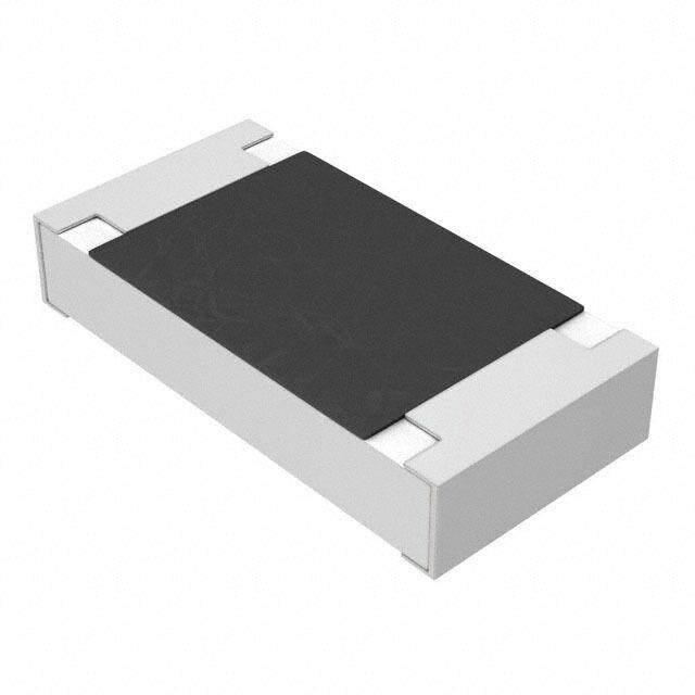
| 描述 | MOSFET NCH 25V 20A DPAKMOSFET 25V 40A N-Channel PowerTrench |
| 产品分类 | FET - 单分离式半导体 |
| FET功能 | 逻辑电平门 |
| FET类型 | MOSFET N 通道,金属氧化物 |
| Id-ContinuousDrainCurrent | 20 A |
| Id-连续漏极电流 | 20 A |
| 品牌 | Fairchild Semiconductor |
| 产品手册 | |
| 产品图片 |
|
| rohs | 符合RoHS无铅 / 符合限制有害物质指令(RoHS)规范要求 |
| 产品系列 | 晶体管,MOSFET,Fairchild Semiconductor FDD6796APowerTrench® |
| 数据手册 | |
| 产品型号 | FDD6796A |
| PCN封装 | |
| Pd-PowerDissipation | 3.7 W |
| Pd-功率耗散 | 3.7 W |
| RdsOn-Drain-SourceResistance | 5.7 mOhms |
| RdsOn-漏源导通电阻 | 5.7 mOhms |
| Vds-Drain-SourceBreakdownVoltage | 25 V |
| Vds-漏源极击穿电压 | 25 V |
| Vgs-Gate-SourceBreakdownVoltage | +/- 20 V |
| Vgs-栅源极击穿电压 | 20 V |
| 上升时间 | 7 ns |
| 下降时间 | 4 ns |
| 不同Id时的Vgs(th)(最大值) | 3V @ 250µA |
| 不同Vds时的输入电容(Ciss) | 1780pF @ 13V |
| 不同Vgs时的栅极电荷(Qg) | 34nC @ 10V |
| 不同 Id、Vgs时的 RdsOn(最大值) | 5.7 毫欧 @ 20A,10V |
| 产品目录页面 | |
| 产品种类 | MOSFET |
| 供应商器件封装 | D-Pak |
| 其它名称 | FDD6796ADKR |
| 典型关闭延迟时间 | 19 ns |
| 功率-最大值 | 3.7W |
| 包装 | Digi-Reel® |
| 单位重量 | 260.370 mg |
| 商标 | Fairchild Semiconductor |
| 安装类型 | 表面贴装 |
| 安装风格 | SMD/SMT |
| 封装 | Reel |
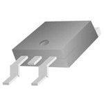
| 封装/外壳 | TO-252-3,DPak(2 引线+接片),SC-63 |
| 封装/箱体 | DPAK-2 |
| 工厂包装数量 | 2500 |
| 晶体管极性 | N-Channel |
| 最大工作温度 | + 175 C |
| 最小工作温度 | - 55 C |
| 标准包装 | 1 |
| 漏源极电压(Vdss) | 25V |
| 电流-连续漏极(Id)(25°C时) | 20A (Ta), 40A (Tc) |
| 系列 | FDD6796 |
| 通道模式 | Enhancement |
| 配置 | Single |


- 商务部:美国ITC正式对集成电路等产品启动337调查
- 曝三星4nm工艺存在良率问题 高通将骁龙8 Gen1或转产台积电
- 太阳诱电将投资9.5亿元在常州建新厂生产MLCC 预计2023年完工
- 英特尔发布欧洲新工厂建设计划 深化IDM 2.0 战略
- 台积电先进制程称霸业界 有大客户加持明年业绩稳了
- 达到5530亿美元!SIA预计今年全球半导体销售额将创下新高
- 英特尔拟将自动驾驶子公司Mobileye上市 估值或超500亿美元
- 三星加码芯片和SET,合并消费电子和移动部门,撤换高东真等 CEO
- 三星电子宣布重大人事变动 还合并消费电子和移动部门
- 海关总署:前11个月进口集成电路产品价值2.52万亿元 增长14.8%


PDF Datasheet 数据手册内容提取
Is Now Part of To learn more about ON Semiconductor, please visit our website at www.onsemi.com ON Semiconductor and the ON Semiconductor logo are trademarks of Semiconductor Components Industries, LLC dba ON Semiconductor or its subsidiaries in the United States and/or other countries. ON Semiconductor owns the rights to a number of patents, trademarks, copyrights, trade secrets, and other intellectual property. A listing of ON Semiconductor’s product/patent coverage may be accessed at www.onsemi.com/site/pdf/Patent-Marking.pdf. ON Semiconductor reserves the right to make changes without further notice to any products herein. ON Semiconductor makes no warranty, representation or guarantee regarding the suitability of its products for any particular purpose, nor does ON Semiconductor assume any liability arising out of the application or use of any product or circuit, and specifically disclaims any and all liability, including without limitation special, consequential or incidental damages. Buyer is responsible for its products and applications using ON Semiconductor products, including compliance with all laws, regulations and safety requirements or standards, regardless of any support or applications information provided by ON Semiconductor. “Typical” parameters which may be provided in ON Semiconductor data sheets and/or specifications can and do vary in different applications and actual performance may vary over time. All operating parameters, including “Typicals” must be validated for each customer application by customer’s technical experts. ON Semiconductor does not convey any license under its patent rights nor the rights of others. ON Semiconductor products are not designed, intended, or authorized for use as a critical component in life support systems or any FDA Class 3 medical devices or medical devices with a same or similar classification in a foreign jurisdiction or any devices intended for implantation in the human body. Should Buyer purchase or use ON Semiconductor products for any such unintended or unauthorized application, Buyer shall indemnify and hold ON Semiconductor and its officers, employees, subsidiaries, affiliates, and distributors harmless against all claims, costs, damages, and expenses, and reasonable attorney fees arising out of, directly or indirectly, any claim of personal injury or death associated with such unintended or unauthorized use, even if such claim alleges that ON Semiconductor was negligent regarding the design or manufacture of the part. ON Semiconductor is an Equal Opportunity/Affirmative Action Employer. This literature is subject to all applicable copyright laws and is not for resale in any manner.
F D D 6 7 March 2015 9 6 FDD6796A / FDU6796A_F071 A / ® F N-Channel PowerTrench MOSFET D U 25 V, 5.7 mΩ 6 7 Features General Description 9 A (cid:132) Max rDS(on) = 5.7 mΩ at VGS = 10 V, ID = 20 A This N-Channel MOSFET has been designed specifically to _F improve the overall efficiency of DC/DC converters using either 0 (cid:132) Max rDS(on) = 15.0 mΩ at VGS = 4.5 V, ID = 15.2 A synchronous or conventional switching PWM controllers. It has 7 1 been optimized for low gate charge, low r and fast (cid:132) 100% UIL tested DS(on) N switching speed. - (cid:132) RoHS Compliant C Applications h a n (cid:132) Vcore DC-DC for Desktop Computers and Servers n e (cid:132) VRM for Intermediate Bus Architecture l P o w e r T r e D n c h ® D M G O G G S D F S E S T Short-Lead I-PAK D-PAK (TO-251AA) S (TO-252) MOSFET Maximum Ratings TC = 25 °C unless otherwise noted Symbol Parameter Ratings Units V Drain to Source Voltage 25 V DS V Gate to Source Voltage ±20 V GS Drain Current -Continuous (Package limited) T = 25 °C 40 C -Continuous (Silicon limited) T = 25 °C 67 I C A D -Continuous T = 25 °C (Note 1a) 20 A -Pulsed 150 E Single Pulse Avalanche Energy (Note 3) 40 mJ AS Power Dissipation T = 25 °C 42 P C W D Power Dissipation T = 25 °C (Note 1a) 3.7 A T , T Operating and Storage Junction Temperature Range -55 to +175 °C J STG Thermal Characteristics R Thermal Resistance, Junction to Case 3.6 θJC °C/W R Thermal Resistance, Junction to Ambient (Note 1a) 40 θJA Package Marking and Ordering Information Device Marking Device Package Reel Size Tape Width Quantity FDD6796A FDD6796A D-PAK (TO-252) 13 ’’ 16 mm 2500 units FDU6796A FDU6796A_F071 TO-251AA N/A(Tube) N/A 75 units ©2009 Fairchild Semiconductor Corporation 1 www.fairchildsemi.com FDD6796A / FDU6796A_F071 Rev. 1.3
F D Electrical Characteristics T = 25 °C unless otherwise noted D J 6 7 Symbol Parameter Test Conditions Min Typ Max Units 9 6 Off Characteristics A BVDSS Drain to Source Breakdown Voltage ID = 250 µA, VGS = 0 V 25 V / F ∆BV Breakdown Voltage Temperature D ∆TDSS Coefficient ID = 250 µA, referenced to 25 °C 16 mV/°C U J 6 IDSS Zero Gate Voltage Drain Current VDS = 20 V, VGS = 0 V 1 µA 7 9 IGSS Gate to Source Leakage Current VGS = ±20 V, VDS = 0 V ±100 nA A _ On Characteristics F 0 V Gate to Source Threshold Voltage V = V , I = 250 µA 1.0 1.9 3.0 V 7 GS(th) GS DS D 1 ∆VGS(th) Gate to Source Threshold Voltage I = 250 µA, referenced to 25 °C -6 mV/°C N ∆TJ Temperature Coefficient D -C VGS = 10 V, ID = 20 A 4.3 5.7 h r Static Drain to Source On Resistance V = 4.5 V, I = 15.2 A 11.1 15.0 mΩ a DS(on) GS D n V = 10 V, I = 20 A, T = 150 °C 6.5 8.6 n GS D J e gFS Forward Transconductance VDS = 5 V, ID = 20 A 118 S l P Dynamic Characteristics o w C Input Capacitance 1336 1780 pF e Ciss Output Capacitance VDS = 13 V, VGS = 0 V, 298 400 pF rT oss f = 1 MHz r C Reverse Transfer Capacitance 266 400 pF e rss n R Gate Resistance 1.2 Ω c g h ® Switching Characteristics M td(on) Turn-On Delay Time 8 16 ns O tr Rise Time VDD = 13 V, ID = 20 A, 7 14 ns SF td(off) Turn-Off Delay Time VGS = 10 V, RGEN = 6 Ω 19 34 ns E t Fall Time 4 10 ns T f Q Total Gate Charge V = 0 V to 10 V 24 34 nC g GS Qg Total Gate Charge VGS = 0 V to 5 V VDD = 13 V, 14 20 nC Qgs Gate to Source Charge ID = 20 A 4.0 nC Q Gate to Drain “Miller” Charge 5.7 nC gd Drain-Source Diode Characteristics V = 0 V, I = 3.1 A (Note 2) 0.8 1.2 V Source to Drain Diode Forward Voltage GS S V SD V = 0 V, I = 20 A (Note 2) 0.9 1.3 GS S t Reverse Recovery Time 15 27 ns rr I = 20 A, di/dt = 100 A/µs Q Reverse Recovery Charge F 4 10 nC rr Notes: 1: RθJA is the sum of the junction-to-case and case-to-ambient thermal resistance where the case thermal reference is defined as the solder mounting surface of the drain pins. RθJC is guaranteed by design while RθJA is determined by the user’s board design. a)40 °C/W when mounted on a b) 96 °C/W when mounted on 1 in2 pad of 2 oz copper a minimum pad 2: Pulse Test: Pulse Width < 300 µs, Duty cycle < 2.0%. 3: EAS of 40 mJ is based on starting TJ = 25 °C, L = 1 mH, IAS = 9 A, VDD = 23 V, VGS = 10 V. 100% test at L = 0.1 mH, IAS = 21 A. ©2009 Fairchild Semiconductor Corporation 2 www.fairchildsemi.com FDD6796A / FDU6796A_F071 Rev. 1.3
F D Typical Characteristics D T = 25 °C unless otherwise noted J 6 7 9 6 150 4 A VGS = 8 V CE PULSE DURATION = 80 µs / RAIN CURRENT (A)1269000 VGS = 10 V VGS = 6 V VVGGS S= = 4 4.5 V V NORMALIZEDOURCE ON-RESISTAN 23 VGS = 3.5 V DUTVVYGG SCS Y== C8 4L VVE = V0G.5S% =V M6G SAV X= 4.5 V FDU679A_F D S 0 , ID 30 PULSE DURATIONV G=S 8 =0 3µ.s5 V AIN TO 1 VGS = 10 V 71 N R DUTY CYCLE = 0.5% MAX D - 0 0 C 0.0 0.5 1.0 1.5 2.0 2.5 0 30 60 90 120 150 h VDS, DRAIN TO SO URCE VOLTAGE (V) ID, DRAIN C URRENT (A) an n e Figure 1. On Region Characteristics Figure 2. Normalized On-Resistance l vs Drain Current and Gate Voltage P o w e 1.8 20 rT ANCE 1.6 IVDG =S 2=0 1 A0 V )mΩ PDUULTSYE C DYUCRLEA T=I O0.N5 %= 8M0A µXs ren NORMALIZED TO SOURCE ON-RESIST 111...024 rDRAIN TO ,DS(on)(RCE ON-RESISTANCE 11055 ID = 20 A TJ = 150 oC chMOSFET® AIN 0.8 SOU TJ = 25 oC R D 0.6 0 -75 -50 -25 0 25 50 75 100 125 150 175 2 4 6 8 10 TJ, JUNCTION TEM PERATURE (oC) VGS, GATE TO SOURCE VOLTAGE (V) Figure 3. Normalized On Resistance Figure 4. On-Resistance vs Gate to vs Junction Temperature Source Voltage 150 200 PULSE DURATION = 80 µs A) 100 DUTY CYCLE = 0.5% MAX T ( 120 N A) VDS = 3 V RE VGS = 0 V T ( UR URREN 90 RAIN C 10 TJ = 175 oC C D RAIN 60 TJ = 175 oC ERSE 1 TJ = 25 oC TJ = -55 oC D V , D 30 RE I TJ = 25 oC TJ = -55 oC I, S 0 0.1 0 1 2 3 4 5 6 0.2 0.4 0.6 0.8 1.0 1.2 VGS, GATE TO SOU RCE VOLTAGE (V) VSD, BODY DIODE FOR WARD VOLTAGE (V) Figure 5. Transfer Characteristics Figure 6. Source to Drain Diode Forward Voltage vs Source Current ©2009 Fairchild Semiconductor Corporation 3 www.fairchildsemi.com FDD6796A / FDU6796A_F071 Rev. 1.3
F D Typical Characteristics T = 25 °C unless otherwise noted D J 6 7 9 6 10 5000 A E (V) ID = 20 A / F G 8 E VOLTA 6 VDD = 10 V CE (pF)1000 Ciss DU67 O SOURC 4 VDD = 13 V VDD = 16 V PACITAN Coss 9A_F T A 0 E C 7 AT 2 1 V, GGS 0 100 fV =G S1 =M 0H Vz Crss N-C 0 5 10 15 20 25 30 0.1 1 10 30 h Qg, GATE CH ARGE (nC) VDS, DRAIN TO SOU RCE VOLTAGE (V) an n e Figure 7. Gate Charge Characteristics Figure 8. Capacitance vs Drain l to Source Voltage P o w e 100 80 r T r e ENT (A) 40 NT (A) 60 nch CURR TJ = 125 oC URRE VGS = 10 V M® HE 10 N C 40 O AVALANC TJ = 150 oC TJ = 25 oC , IDRAID20 Limited by Package SFET , S RθJC = 3.6 oC/W VGS = 4.5 V A I 1 0 0.001 0.01 0.1 1 10 100 25 50 75 100 125 150 175 tAV, TIME IN AVA LANCHE (ms) TC, CASE TEMPERATURE (oC) Figure 9. Unclamped Inductive Figure 10. Maximum Continuous Drain Switching Capability Current vs Case Temperature 200 2000 100 10 us W)1000 VGS = 10 V R ( T (A) OWE N CURREN 10 TLIHMISIT AERDE BAY I SrD S(on) 110 m0 sus ANSIENT P 100 SRTCIθNJ =CG 2=L5 E3 o .PC6 UoCLS/WE AI R DR 1 SINGLE PULSE 10 ms K T I, D TRTJCθ J ==C M 2=5 A3 Xo.C6 R oCA/TWED 1D0C0 ms , PEA)PK 0.1 P( 10 0.1 1 10 100 10-5 10-4 10-3 10-2 10-1 1 10 VDS, DRAIN to SOU RCE VOLTAGE (V) t, PULSE WIDT H (sec) Figure 11. Forward Bias Safe Figure 12. Single Pulse Maximum Operating Area Power Dissipation ©2009 Fairchild Semiconductor Corporation 4 www.fairchildsemi.com FDD6796A / FDU6796A_F071 Rev. 1.3
F D Typical Characteristics T = 25 °C unless otherwise noted D J 6 7 9 6 A 2 / F 1 DUTY CYCLE-DESCENDING ORDER D U AL D = 0.5 6 M C 0.2 7 THER E,ZJθ 00..105 PDM 9A MALIZED MPEDANC 0.1 00..0021 t1t2 _F071 NORI SINGLE PULSE NDOUTTYE SF:ACTOR: D = t1/t2 N R = 3.6 oC/W PEAK TJ = PDM x ZθJC x RθJc + TC -C θJC h a 0.01 n 10-5 10-4 10-3 10-2 10-1 1 n e t, RECTANGULAR PULSE DURATION (sec) l P Figure 13. Junction-to-Case Transient Thermal Response Curve o w e 2 r T 1 r e DUTY CYCLE-DESCENDING ORDER n L c A h ALIZED THERM PEDANCE,ZJAθ 00.0.11 D = 000000......210005521 PDM t1 MOSF® ORMIM NOTES: t2 ET N SINGLE PULSE DUTY FACTOR: D = t1/t2 0.001 RθJA = 96 oC/W PEAK TJ = PDM x ZθJA x RθJA + TA (Note 1b) 0.0005 10-4 10-3 10-2 10-1 1 10 100 1000 t, RECTANGULAR PULSE DURATION (sec) Figure 14. Junction-to-Ambient Transient Thermal Response Curve ©2009 Fairchild Semiconductor Corporation 5 www.fairchildsemi.com FDD6796A / FDU6796A_F071 Rev. 1.3
None
ON Semiconductor and are trademarks of Semiconductor Components Industries, LLC dba ON Semiconductor or its subsidiaries in the United States and/or other countries. ON Semiconductor owns the rights to a number of patents, trademarks, copyrights, trade secrets, and other intellectual property. A listing of ON Semiconductor’s product/patent coverage may be accessed at www.onsemi.com/site/pdf/Patent−Marking.pdf. ON Semiconductor reserves the right to make changes without further notice to any products herein. ON Semiconductor makes no warranty, representation or guarantee regarding the suitability of its products for any particular purpose, nor does ON Semiconductor assume any liability arising out of the application or use of any product or circuit, and specifically disclaims any and all liability, including without limitation special, consequential or incidental damages. Buyer is responsible for its products and applications using ON Semiconductor products, including compliance with all laws, regulations and safety requirements or standards, regardless of any support or applications information provided by ON Semiconductor. “Typical” parameters which may be provided in ON Semiconductor data sheets and/or specifications can and do vary in different applications and actual performance may vary over time. All operating parameters, including “Typicals” must be validated for each customer application by customer’s technical experts. ON Semiconductor does not convey any license under its patent rights nor the rights of others. ON Semiconductor products are not designed, intended, or authorized for use as a critical component in life support systems or any FDA Class 3 medical devices or medical devices with a same or similar classification in a foreign jurisdiction or any devices intended for implantation in the human body. Should Buyer purchase or use ON Semiconductor products for any such unintended or unauthorized application, Buyer shall indemnify and hold ON Semiconductor and its officers, employees, subsidiaries, affiliates, and distributors harmless against all claims, costs, damages, and expenses, and reasonable attorney fees arising out of, directly or indirectly, any claim of personal injury or death associated with such unintended or unauthorized use, even if such claim alleges that ON Semiconductor was negligent regarding the design or manufacture of the part. ON Semiconductor is an Equal Opportunity/Affirmative Action Employer. This literature is subject to all applicable copyright laws and is not for resale in any manner. PUBLICATION ORDERING INFORMATION LITERATURE FULFILLMENT: N. American Technical Support: 800−282−9855 Toll Free ON Semiconductor Website: www.onsemi.com Literature Distribution Center for ON Semiconductor USA/Canada 19521 E. 32nd Pkwy, Aurora, Colorado 80011 USA Europe, Middle East and Africa Technical Support: Order Literature: http://www.onsemi.com/orderlit Phone: 303−675−2175 or 800−344−3860 Toll Free USA/Canada Phone: 421 33 790 2910 Fax: 303−675−2176 or 800−344−3867 Toll Free USA/Canada Japan Customer Focus Center For additional information, please contact your local Email: orderlit@onsemi.com Phone: 81−3−5817−1050 Sales Representative © Semiconductor Components Industries, LLC www.onsemi.com www.onsemi.com 1