ICGOO在线商城 > 集成电路(IC) > PMIC - 栅极驱动器 > FAN7390MX
 Datasheet下载
- 型号: FAN7390MX
- 制造商: Fairchild Semiconductor
- 库位|库存: xxxx|xxxx
- 要求:
| 数量阶梯 | 香港交货 | 国内含税 |
| +xxxx | $xxxx | ¥xxxx |
查看当月历史价格
查看今年历史价格
FAN7390MX产品简介:
ICGOO电子元器件商城为您提供FAN7390MX由Fairchild Semiconductor设计生产,在icgoo商城现货销售,并且可以通过原厂、代理商等渠道进行代购。 FAN7390MX价格参考。Fairchild SemiconductorFAN7390MX封装/规格:PMIC - 栅极驱动器, Half-Bridge Gate Driver IC Non-Inverting 8-SOP。您可以下载FAN7390MX参考资料、Datasheet数据手册功能说明书,资料中有FAN7390MX 详细功能的应用电路图电压和使用方法及教程。
FAN7390MX是由ON Semiconductor(现为安森美半导体)生产的一款PMIC(电源管理集成电路),专门用于栅极驱动器应用。它主要用于驱动MOSFET、IGBT等功率开关器件,广泛应用于各种电力电子设备中。

 应用场景:

1. 太阳能逆变器:
   FAN7390MX可以用于太阳能逆变器中的功率级控制。通过高效驱动MOSFET或IGBT,它可以提高逆变器的效率和可靠性,确保太阳能系统能够稳定地将直流电转换为交流电,供家庭或电网使用。

2. 电机驱动:
   在工业自动化和家电领域,FAN7390MX可用于驱动电机控制器中的功率开关。它能够提供快速且精确的栅极驱动信号,确保电机运行平稳、响应迅速,并减少能耗。

3. 不间断电源(UPS):
   FAN7390MX在UPS系统中起到关键作用,特别是在逆变器和充电电路中。它可以帮助实现高效的电源切换和稳定的电压输出,确保在市电中断时,负载设备能够持续正常工作。

4. 电动汽车(EV)和混合动力汽车(HEV):
   在电动汽车和混合动力汽车的动力总成系统中,FAN7390MX可以用于驱动主逆变器中的功率开关。它能够承受高电压和大电流,确保车辆的电动机和电池管理系统高效运行。

5. 开关电源(SMPS):
   FAN7390MX适用于各种开关电源设计,如服务器电源、通信设备电源等。它能够提供高效的栅极驱动,确保电源系统的稳定性和高效性,同时降低电磁干扰(EMI)。

6. LED驱动器:
   在LED照明系统中,FAN7390MX可以用于驱动功率开关,以实现恒流或恒压控制。它能够确保LED灯具在不同负载条件下保持稳定的亮度和颜色一致性。

 特点:
- 高速驱动能力:支持快速开关操作,减少开关损耗。
- 强大的抗噪性能:能够在复杂电磁环境中稳定工作。
- 低功耗设计:有助于提高整体系统的能效。
- 宽工作电压范围:适应多种应用场景的需求。

总之,FAN7390MX凭借其高性能和可靠性,成为各类电力电子设备中不可或缺的关键组件。
| 参数 | 数值 |
| 产品目录 | 集成电路 (IC)半导体 |
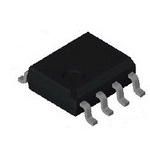
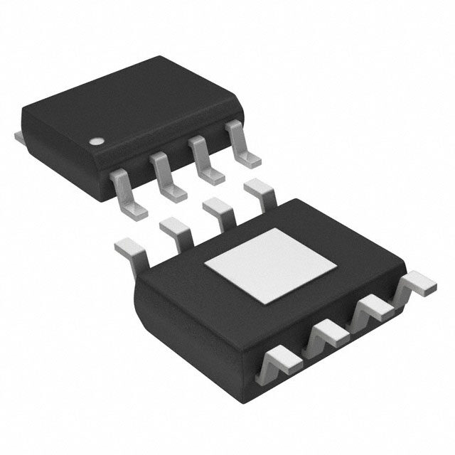
| 描述 | IC DRIVER GATE HI/LO SIDE 8-SOP门驱动器 Half Bridge Gate 600V .625W |
| 产品分类 | PMIC - MOSFET,电桥驱动器 - 外部开关集成电路 - IC |
| 品牌 | Fairchild Semiconductor |
| 产品手册 | |
| 产品图片 |
|
| rohs | 符合RoHS无铅 / 符合限制有害物质指令(RoHS)规范要求 |
| 产品系列 | 电源管理 IC,门驱动器,Fairchild Semiconductor FAN7390MX- |
| 数据手册 | |
| 产品型号 | FAN7390MX |
| PCN组件/产地 | |
| 上升时间 | 25 ns |
| 下降时间 | 20 ns |
| 产品 | MOSFET Gate Drivers |
| 产品目录页面 | |
| 产品种类 | 门驱动器 |
| 供应商器件封装 | 8-SOP |
| 其它名称 | FAN7390MXTR |
| 包装 | 带卷 (TR) |
| 单位重量 | 143 mg |
| 商标 | Fairchild Semiconductor |
| 安装类型 | 表面贴装 |
| 安装风格 | SMD/SMT |
| 封装 | Reel |
| 封装/外壳 | 8-SOIC(0.154",3.90mm 宽) |
| 封装/箱体 | SOP-8 |
| 工作温度 | -40°C ~ 125°C |
| 工厂包装数量 | 3000 |
| 延迟时间 | 140ns |
| 最大功率耗散 | 625 mW |
| 最大工作温度 | + 125 C |
| 最小工作温度 | - 40 C |
| 标准包装 | 3,000 |
| 激励器数量 | 2 Driver |
| 电压-电源 | 10 V ~ 22 V |
| 电流-峰值 | 4.5A |
| 电源电压-最大 | 22 V |
| 电源电压-最小 | 10 V |
| 电源电流 | 0.64 mA |
| 类型 | Half-Bridge Driver |
| 系列 | FAN7390 |
| 输入类型 | 非反相 |
| 输出数 | 2 |
| 输出电流 | 4.5 A |
| 输出端数量 | 2 |
| 配置 | Non-Inverting |
| 配置数 | 1 |
| 高压侧电压-最大值(自举) | 600V |


- 商务部:美国ITC正式对集成电路等产品启动337调查
- 曝三星4nm工艺存在良率问题 高通将骁龙8 Gen1或转产台积电
- 太阳诱电将投资9.5亿元在常州建新厂生产MLCC 预计2023年完工
- 英特尔发布欧洲新工厂建设计划 深化IDM 2.0 战略
- 台积电先进制程称霸业界 有大客户加持明年业绩稳了
- 达到5530亿美元!SIA预计今年全球半导体销售额将创下新高
- 英特尔拟将自动驾驶子公司Mobileye上市 估值或超500亿美元
- 三星加码芯片和SET,合并消费电子和移动部门,撤换高东真等 CEO
- 三星电子宣布重大人事变动 还合并消费电子和移动部门
- 海关总署:前11个月进口集成电路产品价值2.52万亿元 增长14.8%


PDF Datasheet 数据手册内容提取
Is Now Part of To learn more about ON Semiconductor, please visit our website at www.onsemi.com Please note: As part of the Fairchild Semiconductor integration, some of the Fairchild orderable part numbers will need to change in order to meet ON Semiconductor’s system requirements. Since the ON Semiconductor product management systems do not have the ability to manage part nomenclature that utilizes an underscore (_), the underscore (_) in the Fairchild part numbers will be changed to a dash (-). This document may contain device numbers with an underscore (_). Please check the ON Semiconductor website to verify the updated device numbers. The most current and up-to-date ordering information can be found at www.onsemi.com. Please email any questions regarding the system integration to Fairchild_questions@onsemi.com. ON Semiconductor and the ON Semiconductor logo are trademarks of Semiconductor Components Industries, LLC dba ON Semiconductor or its subsidiaries in the United States and/or other countries. ON Semiconductor owns the rights to a number of patents, trademarks, copyrights, trade secrets, and other intellectual property. A listing of ON Semiconductor’s product/patent coverage may be accessed at www.onsemi.com/site/pdf/Patent-Marking.pdf. ON Semiconductor reserves the right to make changes without further notice to any products herein. ON Semiconductor makes no warranty, representation or guarantee regarding the suitability of its products for any particular purpose, nor does ON Semiconductor assume any liability arising out of the application or use of any product or circuit, and specifically disclaims any and all liability, including without limitation special, consequential or incidental damages. Buyer is responsible for its products and applications using ON Semiconductor products, including compliance with all laws, regulations and safety requirements or standards, regardless of any support or applications information provided by ON Semiconductor. “Typical” parameters which may be provided in ON Semiconductor data sheets and/or specifications can and do vary in different applications and actual performance may vary over time. All operating parameters, including “Typicals” must be validated for each customer application by customer’s technical experts. ON Semiconductor does not convey any license under its patent rights nor the rights of others. ON Semiconductor products are not designed, intended, or authorized for use as a critical component in life support systems or any FDA Class 3 medical devices or medical devices with a same or similar classification in a foreign jurisdiction or any devices intended for implantation in the human body. Should Buyer purchase or use ON Semiconductor products for any such unintended or unauthorized application, Buyer shall indemnify and hold ON Semiconductor and its officers, employees, subsidiaries, affiliates, and distributors harmless against all claims, costs, damages, and expenses, and reasonable attorney fees arising out of, directly or indirectly, any claim of personal injury or death associated with such unintended or unauthorized use, even if such claim alleges that ON Semiconductor was negligent regarding the design or manufacture of the part. ON Semiconductor is an Equal Opportunity/Affirmative Action Employer. This literature is subject to all applicable copyright laws and is not for resale in any manner.
F A N 7 3 July 2012 9 0 — H i g h - C FAN7390 u r r High-Current, High & Low-Side, Gate-Drive IC e n t , H i Features Description g h & Floating Channels for Bootstrap Operation to +600V The FAN7390 is a monolithic high- and low-side gate- Typically 4.5A/4.5A Sourcing/Sinking Current Driving drive IC, which can drive high speed MOSFETs and Lo Capability IGBTs that operate up to +600V. It has a buffered output w stage with all NMOS transistors designed for high pulse Common-Mode dv/dt Noise Canceling Circuit S current driving capability and minimum cross-conduction. i Built-in Under-Voltage Lockout for Both Channels d e Matched Propagation Delay for Both Channels Fairchild’s high-voltage process and common-mode , G noise canceling techniques provide stable operation of Logic (VSS) and Power (COM) Ground +/- 7V Offset a the high-side driver under high dv/dt noise circumstances. t 3.3V and 5V Input Logic Compatible e An advanced level shift circuit offers high-side gate driver -D Output In-phase with Input operation up to V =-9.8V (typical) for V =15V. r S BS i v The UVLO circuit prevents malfunction when V and e DD Applications V are lower than the specified threshold voltage. IC BS PDP Sustain Driver The high current and low output voltage drop feature HID Lamp Ballast make this device suitable for the PDP sustain pulse SMPS driver, motor driver, switching power supply, and high- power DC-DC converter applications. Motor Driver 8-SOP 14-SOP Ordering Information Operating Part Number Package Packing Method Temperature Range FAN7390MX 8-SOP Tape & Reel -40C ~ 125C FAN7390M1X 14-SOP Tape & Reel © 2008 Fairchild Semiconductor Corporation www.fairchildsemi.com FAN7390 Rev. 1.0.6
F A Typical Application Circuit N 7 3 9 0 15V — H FAN7390 RBOOT ig Up to 600V h - DBOOT C HIN 1 HIN V 8 u B r r Controller e R1 Q1 n LIN 2 LIN HO 7 t, H CBOOT R2 ig h 3 COM V 6 S & L OUTPUT o 4 LO VDD 5 w Load S C1 i d R3 Q2 e , G a R4 t e - D FAN7390 Rev.01 r i v e Figure 1. Application Circuit for Half-Bridge (Referenced 8-SOP) I C 15V RBOOT DBOOT FAN7390M1 Up to 600V HIN 1 HIN NC 14 Controller LIN 2 LIN V 13 VSS B R1 Q1 3 V HO 12 SS CBOOT R2 4 NC V 11 S 5 COM NC 10 6 LO NC 9 OUTPUT 7 VDD NC 8 Load C1 R3 Q2 R4 FAN7390M1 Rev.03 Figure 2. Application Circuit for Half-Bridge (Referenced 14-SOP) © 2008 Fairchild Semiconductor Corporation www.fairchildsemi.com FAN7390 Rev. 1.0.6 2
F A Internal Block Diagram N 7 3 9 0 — FAN7390 8 VB H i g UVLO h - C D HIN 1 GENEPU NOISE R R RIVER 7 HO urre RALS CANCELLER S Q n 200K TORE t, H 6 VS i g h & 5 VDD L o UVLO w D S LIN 2 DELAY VLSES/VCEOLM RIVE 4 LO id SHIFT R e , 200K G a 3 COM te - D r i v FAN7390 Rev.06 e I Figure 3. Functional Block Diagram (Referenced 8-SOP) C FAN7390M1 13 VB UVLO D HIN 1 GENEPU NOISE R R RIVER 12 HO RALS CANCELLER S Q TE 200K O R 11 VS 7 VDD UVLO D LIN 2 DELAY VLSES/VCEOLM RIVE 6 LO SHIFT R 200K V 3 5 COM SS Pin 4, 8, 9, 10 and 14 are no connection FAN7390M1 Rev.06 Figure 4. Functional Block Diagram (Referenced 14-SOP) © 2008 Fairchild Semiconductor Corporation www.fairchildsemi.com FAN7390 Rev. 1.0.6 3
F A Pin Configurations N 7 3 9 0 — FAN7390M FAN7390M1 H i g h - C HIN 1 8 V HIN 1 14 NC u B r r e LIN 2 7 HO LIN 2 13 V n B FAN7390 t, H COM 3 6 VS VSS 3 12 HO ig h LO 4 5 VDD NC 4 FAN7390M1 11 VS & L o COM 5 10 NC w FAN7390 Rev.01 S LO 6 9 NC id e , VDD 7 8 NC G a t e - D FAN7390M1 Rev.01 r i v Figure 5. Pin Assignments (Top View) e I C Pin Definitions 8-Pin 14-Pin Name Description 1 1 HIN Logic Input for High-Side Gate Driver Output 2 2 LIN Logic Input for Low-Side Gate Driver Output 3 V Logic Ground (FAN7390M1 only) SS 3 5 COM Low-Side Driver Return 4 6 LO Low-Side Driver Output 5 7 V Low-Side and Logic Part Supply Voltage DD 6 11 V High-Voltage Floating Supply Return S 7 12 HO High-Side Driver Output 8 13 V High-Side Floating Supply B 4, 8, 9, 10, 14 NC No Connect © 2008 Fairchild Semiconductor Corporation www.fairchildsemi.com FAN7390 Rev. 1.0.6 4
F A Absolute Maximum Ratings N 7 3 Stresses exceeding the absolute maximum ratings may damage the device. The device may not function or be opera- 9 ble above the recommended operating conditions and stressing the parts to these levels is not recommended. In addi- 0 tion, extended exposure to stresses above the recommended operating conditions may affect device reliability. The — absolute maximum ratings are stress ratings only. TA=25°C, unless otherwise specified. H i Symbol Characteristics Min. Max. Unit g h VS High-Side Floating Supply Offset Voltage VB-25 VB+0.3 V -C u V High-Side Floating Supply Voltage -0.3 625.0 V B r r V High-Side Floating Output Voltage HO V -0.3 V +0.3 V e HO S B n t VDD Low-Side and Logic Fixed Supply Voltage -0.3 25.0 V , H VLO Low-Side Output Voltage LO -0.3 VDD+0.3 V ig h V Logic Input Voltage (HIN and LIN) V -0.3 V +0.3 V IN SS DD & VSS Logic Ground (FAN7390M1 only) VDD-25 VDD+0.3 V L o dV /dt Allowable Offset Voltage Slew Rate 50 V/ns S w 8-SOP 0.625 S PD(1)(2)(3) Power Dissipation 14-SOP 1.000 W id e 8-SOP 200 , G Thermal Resistance, Junction-to-Ambient C/W JA 14-SOP 110 a t e T Junction Temperature +150 C - J D TSTG Storage Temperature +150 C riv e Notes: I C 1. Mounted on 76.2 x 114.3 x 1.6mm PCB (FR-4 glass epoxy material). 2. Refer to the following standards: JESD51-2: Integral circuits thermal test method environmental conditions - natural convection JESD51-3: Low effective thermal conductivity test board for leaded surface mount packages 3. Do not exceed P under any circumstances. D Recommended Operating Conditions The Recommended Operating Conditions table defines the conditions for actual device operation. Recommended operating conditions are specified to ensure optimal performance to the datasheet specifications. Fairchild does not recommend exceeding them or designing to absolute maximum ratings. Symbol Parameter Min. Max. Unit V High-Side Floating Supply Voltage V +10 V +22 V B S S V High-Side Floating Supply Offset Voltage 6-V 600 V S DD V High-Side Output Voltage V V V HO S B V Low-Side and Logic Supply Voltage 10 22 V DD V Low-Side Output Voltage COM V V LO DD V Logic Input Voltage (HIN and LIN) V V V IN SS DD T Operating Ambient Temperature -40 +125 C A © 2008 Fairchild Semiconductor Corporation www.fairchildsemi.com FAN7390 Rev. 1.0.6 5
F A Electrical Characteristics N 7 3 V (V , V )=15.0V, V =V =COM, T =25C, unless otherwise specified. The V , V , and I parameters are BIAS DD BS S SS A IL IH IN 9 referenced to V /COM and are applicable to the respective input signals HIN and LIN. The V and I parameters are 0 SS O O referenced to COM and VS is applicable to the respective output signals HO and LO. — Symbol Characteristics Test Condition Min. Typ. Max. Unit H i g POWER SUPPLY SECTION (V AND V ) DD BS h VDDUV+ VDD and VBS Supply Under-Voltage 8.0 8.8 9.8 -C V Positive-going Threshold u BSUV+ r VVDDUV- NVDeDg aatnivde -VgBoSin Sg uTphprleys Uhonldder-Voltage 7.4 8.3 9.0 V ren BSUV- t , VDDUVH VDD and VBS Supply Under-Voltage 0.5 H VBSUVH Lockout Hysteresis Voltage ig h I Offset Supply Leakage Current V =V =600V 50 LK B S & IQBS Quiescent VBS Supply Current VIN=0V or 5V 45 80 µA L I Quiescent V Supply Current V =0V or 5V 75 110 o QDD DD IN w I Operating V Supply Current f =20kHz, rms value 530 640 PBS BS IN S µA IPDD Operating VDD Supply Current fIN=20kHz, rms value 530 640 id e LOGIC INPUT SECTION (HIN, LIN) , G VIH Logic "1" Input Voltage 2.5 a V t V Logic "0" Input Voltage 1.2 e IL - D I Logic "1" Input Bias Current V =5V 25 50 IN+ IN µA ri I Logic "0" Input Bias Current V =0V 1.0 2.0 v IN- IN e RIN Input Pull-down Resistance 100 200 K IC GATE DRIVER OUTPUT SECTION (HO, LO) V High-level Output Voltage, V -V No Load 1.0 V OH BIAS O V Low-level Output Voltage, V No Load 35 mV OL O Output High, Short-circuit Pulsed I V =0V, V =5V with PW<10µs 3.5 4.5 O+ Current(4) O IN A Output Low, Short-circuit Pulsed V =15V, V =0V with I O IN 3.5 4.5 O- Current(4) PW<10µs Allowable Negative V Pin Voltage for V S -9.8 -7.0 V S HIN Signal Propagation to HO V - SS V -COM/COM-V Voltage Endurability -7.0 7.0 V COM SS SS Note: 4. This parameter guaranteed by design. Dynamic Electrical Characteristics V (V , V )=15.0V, V =V =COM=0V, C =1000pF and T =25C unless otherwise specified. BIAS DD BS S SS L A Symbol Characteristics Test Condition Min. Typ. Max. Unit t Turn-on Propagation Delay V =0V 140 200 on S t Turn-off Propagation Delay V =0V 140 200 off S MT Delay Matching, HS & LS Turn-on/off 0 50 ns t Turn-on Rise Time 25 50 r t Turn-off Fall Time 20 45 f © 2008 Fairchild Semiconductor Corporation www.fairchildsemi.com FAN7390 Rev. 1.0.6 6
F A Typical Characteristics N 7 3 9 0 240 240 — 220 220 H 200 200 ig h 180 180 t [ns] ON 114600 t [ns] OFF 114600 -Curr e 120 120 n t 100 100 , H 80 80 i g 60 60 h -40 -20 0 20 40 60 80 100 120 -40 -20 0 20 40 60 80 100 120 & Temperature [°C] Temperature [°C] L o Figure 6. Turn-on Propagation Delay Figure 7. Turn-off Propagation Delay w vs. Temperature vs. Temperature S i d e , G 40 40 a t e - 30 30 D r i v t [ns] R 20 t [ns] F 20 e IC 10 10 0 0 -40 -20 0 20 40 60 80 100 120 -40 -20 0 20 40 60 80 100 120 Temperature [°C] Temperature [°C] Figure 8. Turn-on Rise Time Figure 9. Turn-off Fall Time vs. Temperature vs. Temperature 50 50 40 40 T [ns] ON 30 T [ns] OFF 2300 M M 20 10 10 0 0 -10 -40 -20 0 20 40 60 80 100 120 -40 -20 0 20 40 60 80 100 120 Temperature [°C] Temperature [°C] Figure 10. Turn-on Delay Matching vs. Temperature Figure 11. Turn-off Delay Matching vs. Temperature © 2008 Fairchild Semiconductor Corporation www.fairchildsemi.com FAN7390 Rev. 1.0.6 7
F A Typical Characteristics (Continued) N 7 3 9 0 — 140 120 H 120 100 ig h ]A 100 ]A 80 -C [ 80 [ u I QDD 60 I QBS 60 rre n 40 t 40 , H 20 20 ig h 0 0 & -40 -20 0 20 40 60 80 100 120 -40 -20 0 20 40 60 80 100 120 L Temperature [°C] Temperature [°C] o w Figure 12. Quiescent V Supply Current Figure 13. Quiescent V Supply Current S DD BS i vs. Temperature vs. Temperature d e , G a 1000 1000 te - D r 800 800 iv []I A PDD 600 []I A PBS 600 e IC 400 400 200 200 -40 -20 0 20 40 60 80 100 120 -40 -20 0 20 40 60 80 100 120 Temperature [°C] Temperature [°C] Figure 14. Operating V Supply Current Figure 15. Operating V Supply Current DD BS vs. Temperature vs. Temperature. 9.5 9.0 9.0 8.5 V] V] V [DDUV+ 8.5 V [DDUV- 8.0 8.0 7.5 7.5 7.0 -40 -20 0 20 40 60 80 100 120 -40 -20 0 20 40 60 80 100 120 Temperature [°C] Temperature [°C] Figure 16. V UVLO+ vs. Temperature Figure 17. V UVLO- vs. Temperature DD DD © 2008 Fairchild Semiconductor Corporation www.fairchildsemi.com FAN7390 Rev. 1.0.6 8
F A Typical Characteristics (Continued) N 7 3 9 0 — 9.5 9.0 H i g h 9.0 8.5 - V [V] BSUV+ 8.5 V [V] BSUV- 8.0 Curren t , 8.0 7.5 H i g h 7.5 7.0 & -40 -20 0 20 40 60 80 100 120 -40 -20 0 20 40 60 80 100 120 L Temperature [°C] Temperature [°C] o w Figure 18. V UVLO+ vs. Temperature Figure 19. V UVLO- vs. Temperature S BS BS i d e , G a t 1500 20 e - D r 1200 i 10 v e mV] 900 mV] IC [OH [OL 0 V V 600 -10 300 0 -20 -40 -20 0 20 40 60 80 100 120 -40 -20 0 20 40 60 80 100 120 Temperature [°C] Temperature [°C] Figure 20. High-Level Output Voltage Figure 21. Low-Level Output Voltage vs. Temperature vs. Temperature 3.0 3.0 2.5 2.5 V] 2.0 V] 2.0 V [IH 1.5 V [IL 1.5 1.0 1.0 0.5 0.5 -40 -20 0 20 40 60 80 100 120 -40 -20 0 20 40 60 80 100 120 Temperature [°C] Temperature [°C] Figure 22. Logic High Input Voltage Figure 23. Low Input Voltage vs. Temperature vs. Temperature © 2008 Fairchild Semiconductor Corporation www.fairchildsemi.com FAN7390 Rev. 1.0.6 9
F A Typical Characteristics (Continued) N 7 3 9 0 — 60 -7 H 50 ig -8 h 40 - C []I A IN+ 2300 V [V] S -1-09 urren t 10 , H -11 0 ig h -10 -12 & -40 -20 0 20 40 60 80 100 120 -40 -20 0 20 40 60 80 100 120 Temperature [°C] Temperature [°C] L o w Figure 24. Logic Input High Bias Current Figure 25. Allowable Negative V Voltage S S i vs. Temperature vs. Temperature d e , G a t e - D r i v e I C . © 2008 Fairchild Semiconductor Corporation www.fairchildsemi.com FAN7390 Rev. 1.0.6 10
F A Switching Time Definitions N 7 3 9 0 15V — HIN 1 HIN VB 8 H i g LIN 2 LIN HO 7 10µF 100nF h - C 1nF u 3 COM VS 6 r r e 15V n 4 LO VDD 5 t, 1nF H 10µF 100nF i g FAN7390 Rev.01 h & L o Figure 26. Switching Time Test Circuit (Referenced 8-SOP) w S i d HIN e LIN , G a t e HO - D LO r i v FAN7390 Rev.01 e I Figure 27. Input/Output Timing Diagram C HIN 50% 50% LIN ton tr toff tf 90% 90% HO LO 10% 10% FAN7390 Rev.01 Figure 28. Switching Time Waveform Definitions HIN 50% 50% LIN LO MT HO 10% 10% 90% 90% LO HO MT FAN7390 Rev.01 Figure 29. Delay Matching Waveform Definitions © 2008 Fairchild Semiconductor Corporation www.fairchildsemi.com FAN7390 Rev. 1.0.6 11
F A Physical Dimensions N 7 3 9 0 — H i g h - C u r r e n t , H i g h & L o w S i d e , G a t e - D r i v e I C Figure 30. 8-Lead Small Outline Package (SOP) Package drawings are provided as a service to customers considering Fairchild components. Drawings may change in any manner without notice. Please note the revision and/or date on the drawing and contact a Fairchild Semiconductor representative to verify or obtain the most recent revision. Package specifications do not expand the terms of Fairchild’s worldwide terms and conditions, specifically the warranty therein, which covers Fairchild products. Always visit Fairchild Semiconductor’s online packaging area for the most recent package drawings: http://www.fairchildsemi.com/packaging/. © 2008 Fairchild Semiconductor Corporation www.fairchildsemi.com FAN7390 Rev. 1.0.6 12
F A Physical Dimensions (Continued) N 7 3 9 0 — H i g h - C u r r e n t , H i g h & L o w S i d e , G a t e - D r i v e I C Figure 31. 14-Lead Small Outline Package (SOP) Package drawings are provided as a service to customers considering Fairchild components. Drawings may change in any manner without notice. Please note the revision and/or date on the drawing and contact a Fairchild Semiconductor representative to verify or obtain the most recent revision. Package specifications do not expand the terms of Fairchild’s worldwide terms and conditions, specifically the warranty therein, which covers Fairchild products. Always visit Fairchild Semiconductor’s online packaging area for the most recent package drawings: http://www.fairchildsemi.com/packaging/. © 2008 Fairchild Semiconductor Corporation www.fairchildsemi.com FAN7390 Rev. 1.0.6 13
F A N 7 3 9 0 — H i g h - C u r r e n t , H i g h & L o w S i d e , G a t e - D r i v e I C © 2008 Fairchild Semiconductor Corporation www.fairchildsemi.com FAN7390 Rev. 1.0.6 14
ON Semiconductor and are trademarks of Semiconductor Components Industries, LLC dba ON Semiconductor or its subsidiaries in the United States and/or other countries. ON Semiconductor owns the rights to a number of patents, trademarks, copyrights, trade secrets, and other intellectual property. A listing of ON Semiconductor’s product/patent coverage may be accessed at www.onsemi.com/site/pdf/Patent−Marking.pdf. ON Semiconductor reserves the right to make changes without further notice to any products herein. ON Semiconductor makes no warranty, representation or guarantee regarding the suitability of its products for any particular purpose, nor does ON Semiconductor assume any liability arising out of the application or use of any product or circuit, and specifically disclaims any and all liability, including without limitation special, consequential or incidental damages. Buyer is responsible for its products and applications using ON Semiconductor products, including compliance with all laws, regulations and safety requirements or standards, regardless of any support or applications information provided by ON Semiconductor. “Typical” parameters which may be provided in ON Semiconductor data sheets and/or specifications can and do vary in different applications and actual performance may vary over time. All operating parameters, including “Typicals” must be validated for each customer application by customer’s technical experts. ON Semiconductor does not convey any license under its patent rights nor the rights of others. ON Semiconductor products are not designed, intended, or authorized for use as a critical component in life support systems or any FDA Class 3 medical devices or medical devices with a same or similar classification in a foreign jurisdiction or any devices intended for implantation in the human body. Should Buyer purchase or use ON Semiconductor products for any such unintended or unauthorized application, Buyer shall indemnify and hold ON Semiconductor and its officers, employees, subsidiaries, affiliates, and distributors harmless against all claims, costs, damages, and expenses, and reasonable attorney fees arising out of, directly or indirectly, any claim of personal injury or death associated with such unintended or unauthorized use, even if such claim alleges that ON Semiconductor was negligent regarding the design or manufacture of the part. ON Semiconductor is an Equal Opportunity/Affirmative Action Employer. This literature is subject to all applicable copyright laws and is not for resale in any manner. PUBLICATION ORDERING INFORMATION LITERATURE FULFILLMENT: N. American Technical Support: 800−282−9855 Toll Free ON Semiconductor Website: www.onsemi.com Literature Distribution Center for ON Semiconductor USA/Canada 19521 E. 32nd Pkwy, Aurora, Colorado 80011 USA Europe, Middle East and Africa Technical Support: Order Literature: http://www.onsemi.com/orderlit Phone: 303−675−2175 or 800−344−3860 Toll Free USA/Canada Phone: 421 33 790 2910 Fax: 303−675−2176 or 800−344−3867 Toll Free USA/Canada Japan Customer Focus Center For additional information, please contact your local Email: orderlit@onsemi.com Phone: 81−3−5817−1050 Sales Representative © Semiconductor Components Industries, LLC www.onsemi.com www.onsemi.com 1
Mouser Electronics Authorized Distributor Click to View Pricing, Inventory, Delivery & Lifecycle Information: O N Semiconductor: FAN7390M FAN7390M1 FAN7390M1X FAN7390N FAN7390MX