ICGOO在线商城 > 集成电路(IC) > PMIC - 栅极驱动器 > FAN7388MX
 Datasheet下载
- 型号: FAN7388MX
- 制造商: Fairchild Semiconductor
- 库位|库存: xxxx|xxxx
- 要求:
| 数量阶梯 | 香港交货 | 国内含税 |
| +xxxx | $xxxx | ¥xxxx |
查看当月历史价格
查看今年历史价格
FAN7388MX产品简介:
ICGOO电子元器件商城为您提供FAN7388MX由Fairchild Semiconductor设计生产,在icgoo商城现货销售,并且可以通过原厂、代理商等渠道进行代购。 FAN7388MX价格参考。Fairchild SemiconductorFAN7388MX封装/规格:PMIC - 栅极驱动器, Half-Bridge Gate Driver IC Non-Inverting 20-SOIC。您可以下载FAN7388MX参考资料、Datasheet数据手册功能说明书,资料中有FAN7388MX 详细功能的应用电路图电压和使用方法及教程。
FAN7388MX是安森美(ON Semiconductor)推出的一款双通道高压栅极驱动器,属于PMIC中的栅极驱动器类别。该器件广泛应用于需要高效、紧凑型电源设计的场景。

其主要应用场景包括:
1. 开关电源(SMPS):适用于半桥、全桥及推挽式拓扑结构,常用于服务器、通信设备和工业电源中,实现高效率能量转换。
2. DC-DC 转换器:在高频率DC-DC变换电路中驱动功率MOSFET或IGBT,提升系统响应速度与能效。
3. 电机驱动:用于小型电机控制电路,如家用电器或工业自动化设备中的三相逆变器,提供稳定可靠的栅极驱动信号。
4. 照明电源:适用于高强度放电灯(HID)、LED驱动电源等电子镇流器应用。

FAN7388MX采用SO-8封装,集成高边与低边驱动通道,支持高达20V的电源电压,具备良好的噪声抑制能力和快速传播延迟特性,适合高频工作环境。同时,其内置的电平移位技术可有效驱动高边N沟道MOSFET,降低系统成本与体积。此外,器件还具有欠压锁定(UVLO)保护功能,提升系统可靠性。

综上,FAN7388MX凭借高集成度、高可靠性和小封装优势,适用于对空间和效率要求较高的工业、消费类及通信电源系统。
| 参数 | 数值 |
| 产品目录 | 集成电路 (IC)半导体 |
| 描述 | IC GATE DRIVER HALF BRIDG 20SOIC门驱动器 3Ch Half Bridge Gate |
| 产品分类 | PMIC - MOSFET,电桥驱动器 - 外部开关集成电路 - IC |
| 品牌 | Fairchild Semiconductor |
| 产品手册 | |
| 产品图片 |
|
| rohs | 符合RoHS无铅 / 符合限制有害物质指令(RoHS)规范要求 |
| 产品系列 | 电源管理 IC,门驱动器,Fairchild Semiconductor FAN7388MX- |
| 数据手册 | |
| 产品型号 | FAN7388MX |
| 上升时间 | 50 ns |
| 下降时间 | 30 ns |
| 产品 | MOSFET Gate Drivers |
| 产品目录页面 | |
| 产品种类 | 门驱动器 |
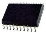
| 供应商器件封装 | 20-SOIC |
| 其它名称 | FAN7388MXCT |
| 包装 | 剪切带 (CT) |
| 单位重量 | 801 mg |
| 商标 | Fairchild Semiconductor |
| 安装类型 | 表面贴装 |
| 安装风格 | SMD/SMT |
| 封装 | Reel |
| 封装/外壳 | 20-SOIC(0.295",7.50mm 宽) |
| 封装/箱体 | SOIC-20 |
| 工作温度 | -40°C ~ 125°C |
| 工厂包装数量 | 1000 |
| 延迟时间 | 130ns |
| 最大功率耗散 | 1.47 W |
| 最大工作温度 | + 125 C |
| 最小工作温度 | - 40 C |
| 标准包装 | 1 |
| 激励器数量 | 3 Driver |
| 电压-电源 | 10 V ~ 20 V |
| 电流-峰值 | 350mA |
| 电源电压-最大 | 20 V |
| 电源电压-最小 | 10 V |
| 电源电流 | 0.9 mA |
| 类型 | 3 Phase Driver |
| 系列 | FAN7388 |
| 输入类型 | 非反相 |
| 输出数 | 3 |
| 输出电流 | 650 mA |
| 输出端数量 | 6 |
| 配置 | Non-Inverting |
| 配置数 | 1 |
| 高压侧电压-最大值(自举) | 600V |


- 商务部:美国ITC正式对集成电路等产品启动337调查
- 曝三星4nm工艺存在良率问题 高通将骁龙8 Gen1或转产台积电
- 太阳诱电将投资9.5亿元在常州建新厂生产MLCC 预计2023年完工
- 英特尔发布欧洲新工厂建设计划 深化IDM 2.0 战略
- 台积电先进制程称霸业界 有大客户加持明年业绩稳了
- 达到5530亿美元!SIA预计今年全球半导体销售额将创下新高
- 英特尔拟将自动驾驶子公司Mobileye上市 估值或超500亿美元
- 三星加码芯片和SET,合并消费电子和移动部门,撤换高东真等 CEO
- 三星电子宣布重大人事变动 还合并消费电子和移动部门
- 海关总署:前11个月进口集成电路产品价值2.52万亿元 增长14.8%


PDF Datasheet 数据手册内容提取
Is Now Part of To learn more about ON Semiconductor, please visit our website at www.onsemi.com Please note: As part of the Fairchild Semiconductor integration, some of the Fairchild orderable part numbers will need to change in order to meet ON Semiconductor’s system requirements. Since the ON Semiconductor product management systems do not have the ability to manage part nomenclature that utilizes an underscore (_), the underscore (_) in the Fairchild part numbers will be changed to a dash (-). This document may contain device numbers with an underscore (_). Please check the ON Semiconductor website to verify the updated device numbers. The most current and up-to-date ordering information can be found at www.onsemi.com. Please email any questions regarding the system integration to Fairchild_questions@onsemi.com. ON Semiconductor and the ON Semiconductor logo are trademarks of Semiconductor Components Industries, LLC dba ON Semiconductor or its subsidiaries in the United States and/or other countries. ON Semiconductor owns the rights to a number of patents, trademarks, copyrights, trade secrets, and other intellectual property. A listing of ON Semiconductor’s product/patent coverage may be accessed at www.onsemi.com/site/pdf/Patent-Marking.pdf. ON Semiconductor reserves the right to make changes without further notice to any products herein. ON Semiconductor makes no warranty, representation or guarantee regarding the suitability of its products for any particular purpose, nor does ON Semiconductor assume any liability arising out of the application or use of any product or circuit, and specifically disclaims any and all liability, including without limitation special, consequential or incidental damages. Buyer is responsible for its products and applications using ON Semiconductor products, including compliance with all laws, regulations and safety requirements or standards, regardless of any support or applications information provided by ON Semiconductor. “Typical” parameters which may be provided in ON Semiconductor data sheets and/or specifications can and do vary in different applications and actual performance may vary over time. All operating parameters, including “Typicals” must be validated for each customer application by customer’s technical experts. ON Semiconductor does not convey any license under its patent rights nor the rights of others. ON Semiconductor products are not designed, intended, or authorized for use as a critical component in life support systems or any FDA Class 3 medical devices or medical devices with a same or similar classification in a foreign jurisdiction or any devices intended for implantation in the human body. Should Buyer purchase or use ON Semiconductor products for any such unintended or unauthorized application, Buyer shall indemnify and hold ON Semiconductor and its officers, employees, subsidiaries, affiliates, and distributors harmless against all claims, costs, damages, and expenses, and reasonable attorney fees arising out of, directly or indirectly, any claim of personal injury or death associated with such unintended or unauthorized use, even if such claim alleges that ON Semiconductor was negligent regarding the design or manufacture of the part. ON Semiconductor is an Equal Opportunity/Affirmative Action Employer. This literature is subject to all applicable copyright laws and is not for resale in any manner.
F A N 7 3 April 2016 8 8 — FAN7388 3 H a 3 Half-Bridge Gate-Drive IC l f - B r i d Features Description g e Floating Channel for Bootstrap Operation to +600 V The FAN7388 is a monolithic three half-bridge gate-drive G Typically 350 mA / 650 mA Sourcing/Sinking Current IC designed for high-voltage, high-speed driving MOS- a t Driving Capability for All Channels FETs and IGBTs operating up to +600 V. e - D 3 Half-Bridge Gate Driver Fairchild’s high-voltage process and common-mode r Extended Allowable Negative VS Swing to -9.8 V for noise canceling technique provide stable operation of iv e Signal Propagation at VBS=15 V high-side drivers under high-dv/dt noise circumstances. I C Matched Propagation Delay Time Maximum: 50 ns An advanced level-shift circuit allows high-side gate 3.3 V and 5 V Input Logic Compatible driver operation up to VS=-9.8 V (typical) for VBS=15 V. Built-in Shoot-Through Prevention Circuit for All The UVLO circuits prevent malfunction when V and DD Channels with 270 ns Typical Dead Time V are lower than the specified threshold voltage. BS Built-in Common Mode dv/dt Noise Canceling Circuit Output drivers typically source/sink 350 mA / 650 mA, Built-in UVLO Functions for All Channels respectively, which is suitable for three-phase half-bridge Applications applications in motor drive systems. 3-Phase Motor Inverter Driver Related Resources 20-SOIC AN-6076 - Design and Application Guide of Bootstrap Circuit for High-Voltage Gate-Drive IC AN-9052 - Design Guide for Selection of Bootstrap Components AN-8102 - Recommendations to Avoid Short Pulse Width Issues in HVIC Gate Driver Applications Ordering Information Operating Part Number Package Temperature Range Packing Method FAN7388MX 20-SOIC -40°C to +125°C Tape & Reel © 2008 Fairchild Semiconductor Corporation www.fairchildsemi.com FAN7388 • Rev. 1.3
F A Typical Application Circuit N 7 3 +15V 8 8 — 3 Up to 600V H a l UU 1 HIN1 VB1 20 f- B UL 2 LIN1 HO1 19 ri d 3B-LPDhCas Me otorVU 3 HIN2 F VS1 18 VS1Q1 Q3 Q5 ge Controller VL 4 LIN2 A LO1 17 Q1 G WU 5 HIN3 N VB2 16 QQ35 VS1 IU ate WL 6 LIN3 73 HO2 15 3-Phase Inverter U -D r 7 LO3 88 VS2 14 VS2 VS2 IV V W ive Q4 8 VS3 LO2 13 QQ62 VS3 IW IC 9 HO3 VDD 12 Q4 Q6 Q2 10 VB3 GND 11 VS3 FAN7388 Rev.00 Figure 1. 3-Phase BLDC Motor Drive Application Internal Block Diagram VB1 UVLO HIN1 UHIN GENERATOPULSE CANNCOEISLELER SR R Q DRIVER VHSO11 R HIN2 VDD_UVLO UVLO VDD SCHMITT TRIGGER INPUT D ULIN R LO1 DELAY IV HIN3 ER VDD GND U Phase Driver LIN1 SHOOT-THOUGH PREVENTION VDD VB2 LIN2 VHIN V Phase Driver HO2 VS2 VLIN LO2 LIN3 CONTROL LOGIC VDD VB3 W Phase Driver HO3 WHIN VS3 WLIN LO3 FAN7388 Rev.01 Figure 2. Functional Block Diagram © 2008 Fairchild Semiconductor Corporation www.fairchildsemi.com FAN7388 • Rev.1.3 2
F A Pin Configuration N 7 3 8 8 HIN1 1 20 VB1 — LIN1 2 19 HO1 3 H HIN2 3 18 V a S1 l F f - LIN2 4 A 17 LO1 B r i HIN3 5 N 16 VB2 dg 7 e LIN3 6 3 15 HO2 G a LO3 7 8 14 VS2 te 8 - D VS3 8 13 LO2 r i v HO3 9 12 VDD e I C VB3 10 11 GND FAN7388 Rev.00 Figure 3. Pin Configuration (Top View) Pin Definitions Pin # Name Description 1 HIN1 Logic input 1 for high-side gate 1 driver 2 LIN1 Logic input 1 for low-side gate 1 driver 3 HIN2 Logic input 2 for high-side gate 2 driver 4 LIN2 Logic input 2 for low-side gate 2 driver 5 HIN3 Logic input 3 for high-side gate 3 driver 6 LIN3 Logic input 3 for low-side gate 3 driver 7 LO3 Low-side gate driver 3 output 8 V High-side driver 3 floating supply offset voltage S3 9 HO3 High-side driver 3 gate driver output 10 V High-side driver 3 floating supply voltage B3 11 GND Ground 12 V Logic and all low-side gate drivers power supply voltage DD 13 LO2 Low-side gate driver 2 output 14 V High-side driver 2 floating supply offset voltage S2 15 HO2 High-side driver 2 gate driver output 16 V High-side driver 2 floating supply voltage B2 17 LO1 Low-side gate driver 1 output 18 V High-side driver 1 floating supply offset voltage S1 19 HO1 High-side driver 1 gate driver output 20 V High-side driver 1 floating supply voltage B1 © 2008 Fairchild Semiconductor Corporation www.fairchildsemi.com FAN7388 • Rev.1.3 3
F A Absolute Maximum Ratings N 7 3 Stresses exceeding the absolute maximum ratings may damage the device. The device may not function or be opera- 8 ble above the recommended operating conditions and stressing the parts to these levels is not recommended. In addi- 8 tion, extended exposure to stresses above the recommended operating conditions may affect device reliability. The — absolute maximum ratings are stress ratings only. TA=25°C, unless otherwise specified. 3 Symbol Parameter Min. Max. Unit H a V High-Side Floating Supply Voltage of V -0.3 625.0 V lf B B1,2,3 - B VS High-Side Floating Supply Offset Voltage of VS1,2,3 VB1,2,3-25 VB1,2,3+0.3 V r i d VHO1,2,3 High-Side Floating Output Voltage VS1,2,3-0.3 VB1,2,3+0.3 V g e VDD Low-Side and Logic-fixed Supply Voltage -0.3 25.0 V G V Low-Side Output Voltage -0.3 V +0.3 V a LO1,2,3 DD t e VIN Logic Input Voltage (HIN1,2,3 and LIN1,2,3) -0.3 VDD+0.3 V -D dV /dt Allowable Offset Voltage Slew Rate 50 V/ns r S i v P Power Dissipation(1)(2)(3) 1.47 W e D I Thermal Resistance, Junction-to-ambient 85 C/W C JA T Junction Temperature +150 C J T Storage Temperature -55 +150 C STG Notes: 1. Mounted on 76.2 x 114.3 x 1.6 mm PCB (FR-4 glass epoxy material). 2. Refer to the following standards: JESD51-2: Integral circuits thermal test method environmental conditions - natural convection JESD51-3: Low effective thermal conductivity test board for leaded surface-mount packages. 3. Do not exceed P under any circumstances. D Recommended Operating Conditions The Recommended Operating Conditions table defines the conditions for actual device operation. Recommended operating conditions are specified to ensure optimal performance to the datasheet specifications. Fairchild does not recommend exceeding them or designing to Absolute Maximum Ratings. Symbol Parameter Min. Max. Unit V High-Side Floating Supply Voltage V +10 V +20 V B1,2,3 S1,2,3 S1,2,3 V High-Side Floating Supply Offset Voltage 6-V 600 V S1,2,3 DD V Supply Voltage 10 20 V DD V High-Side Output Voltage V V V HO1,2,3 S1,2,3 B1,2,3 V Low-Side Output Voltage GND V V LO1,2,3 DD V Logic Input Voltage (HIN1,2,3 and LIN1,2,3) GND V V IN DD T Ambient Temperature -40 +125 °C A © 2008 Fairchild Semiconductor Corporation www.fairchildsemi.com FAN7388 • Rev.1.3 4
F A Electrical Characteristics N 7 3 V (V , V )=15.0 V, T =25C, unless otherwise specified. The V and I parameters are referenced to BIAS DD BS1,2,3 A IN IN 8 GND. The V and I parameters are referenced to GND and V and are applicable to the respective outputs 8 O O S1,2,3 LO1,2,3 and HO1,2,3. — Symbol Characteristics Condition Min. Typ. Max. Unit 3 H LOW-SIDE POWER SUPPLY SECTION a l f I Quiescent V Supply Current V =0 V or 5 V 160 350 µA - QDD DD LIN1,2,3 B I Operating VDD Supply Current for each f =20 kHz, rms Value 500 900 µA rid PDD1,2,3 Channel LIN1,2,3 g e V VDD Supply Under-Voltage Positive-Going V =Sweep, V =15 V 7.2 8.2 9.0 V G DDUV+ Threshold DD BS a t V Supply Under-Voltage Negative-Going e V DD V =Sweep, V =15 V 6.8 7.8 8.5 V - DDUV- Threshold DD BS D r i V Supply Under-Voltage Lockout v VDDHYS HDysDt eresis VDD=Sweep, VBS=15 V 0.4 V e I C BOOTSTRAPPED POWER SUPPLY SECTION Quiescent V Supply Current for each I BS V =0 V or 5 V 50 120 µA QBS1,2,3 Channel HIN1,2,3 Operating V Supply Current for each I BS f =20 kHz, rms Value 400 800 µA PBS1,2,3 Channel HIN1,2,3 V Supply Under-Voltage Positive-going V BS V =15 V, V =Sweep 7.2 8.2 9.0 V BSUV+ Threshold DD BS V Supply Under-Voltage Negative-going V BS V =15 V, V =Sweep 6.8 7.8 8.5 V BSUV- Threshold DD BS V Supply Under-Voltage Lockout V BS V =15 V, V =Sweep 0.4 V BSHYS Hysteresis DD BS I Offset Supply Leakage Current V =V =600 V 10 µA LK B1,2,3 S1,2,3 GATE DRIVER OUTPUT SECTION V High-Level Output Voltage, V -V I =20 mA 1.0 V OH BIAS O O V Low-Level Output Voltage, V I =20 mA 0.6 V OL O O Output HIGH Short-Circuit Pulsed V =0 V, V =5 V with PW I O IN 250 350 mA O+ Current(4) <10 µs V =15 V, V =0 V with PW mA I Output LOW Short-Circuit Pulsed Current(4) O IN 500 650 O- <10 µs Allowable Negative V Pin Voltage for IN V S -9.8 -7.0 V S Signal Propagation to H O LOGIC INPUT SECTION (HIN, LIN) V Logic "1" Input Voltage 2.5 V IH V Logic "0" Input Voltage 1.0 V IL I Logic "1" Input Bias Current V =5 V 25 50 µA IN+ IN I Logic "0" Input Bias Current(4) V =0 V 2.0 µA IN- IN R Input Pull-Down Resistance 100 200 300 K IN Note: 4. This parameter is guaranteed by design. © 2008 Fairchild Semiconductor Corporation www.fairchildsemi.com FAN7388 • Rev.1.3 5
F A Dynamic Electrical Characteristics N 7 T =25C, V (V , V )=15.0 V, V =GND, C =1000 pF unless otherwise specified. 3 A BIAS DD BS1,2,3 S1,2,3 Load 8 8 Symbol Parameter Conditions Min. Typ. Max. Unit — tON Turn-on Propagation Delay VS1,2,3=0 V 130 220 ns 3 t Turn-off Propagation Delay V =0 V 150 240 ns H OFF S1,2,3 a t Turn-on Rise Time 50 120 ns l R f - B t Turn-off Fall Time 30 80 ns F r i MT1 Turn-on Delay Matching I t -t I 50 ns d ON(H) OFF(L) g MT2 Turn-off Delay Matching I t -t I 50 ns e OFF(H) ON(L) G DT Dead Time 100 270 440 ns a t MDT Dead-time Matching I t -t I 60 ns e DT1 DT2 - D r i v e I C © 2008 Fairchild Semiconductor Corporation www.fairchildsemi.com FAN7388 • Rev.1.3 6
F A Typical Characteristics N 7 3 8 8 — 250 300 3 250 H 200 a [ns] ON 150 [ns] OFF 125000 lf-Bri t t d 100 g 100 e G 50 50 a t e 0 0 - D -40 -20 0 20 40 60 80 100 120 -40 -20 0 20 40 60 80 100 120 r Temperature [°C] Temperature [°C] iv e I Figure 4. Turn-on Propagation Delay vs. Temp. Figure 5. Turn-off Propagation Delay vs. Temp. C 120 100 100 80 80 ns] ns] 60 t [R 60 t [F 40 40 20 20 0 0 -40 -20 0 20 40 60 80 100 120 -40 -20 0 20 40 60 80 100 120 Temperature [°C] Temperature [°C] Figure 6. Turn-on Rise Time vs. Temp. Figure 7. Turn-off Fall Time vs. Temp. 50 50 40 40 1 [ns] 30 2 [ns] 30 T T M M 20 20 10 10 0 0 -40 -20 0 20 40 60 80 100 120 -40 -20 0 20 40 60 80 100 120 Temperature [°C] Temperature [°C] Figure 8. Turn-on Delay Matching vs. Temp. Figure 9. Turn-off Delay Matching vs. Temp. © 2008 Fairchild Semiconductor Corporation www.fairchildsemi.com FAN7388 • Rev.1.3 7
F A Typical Characteristics (Continued) N 7 3 8 8 — 500 60 3 H 50 a 400 l f s] s] 40 -B n n DT [ 300 DT [ 30 rid M g e 20 200 G a 10 t e - 100 D 0 -40 -20 0 20 40 60 80 100 120 -40 -20 0 20 40 60 80 100 120 ri Temperature [°C] v Temperature [°C] e I C Figure 10. Dead Time vs. Temp. Figure 11. Dead-Time Matching vs. Temp. 350 120 300 100 ] 250 ] 80 A A [ 200 [ I QDD 150 I QBS 60 40 100 50 20 0 0 -40 -20 0 20 40 60 80 100 120 -40 -20 0 20 40 60 80 100 120 Temperature [°C] Temperature [°C] Figure 12. Quiescent V Supply Current Figure 13. Quiescent V Supply Current DD BS vs. Temp. vs. Temp. 1000 1000 800 800 ] ] A A 600 600 [ [ I PDD 400 I PBS400 200 200 0 0 -40 -20 0 20 40 60 80 100 120 -40 -20 0 20 40 60 80 100 120 Temperature [°C] Temperature [°C] Figure 14. Operating V Supply Current vs. Temp. Figure 15. Operating V Supply Current vs. Temp. DD BS © 2008 Fairchild Semiconductor Corporation www.fairchildsemi.com FAN7388 • Rev. 1.3 8
F A Typical Characteristics (Continued) N 7 3 8 8 — 9.0 9.0 3 H a 8.5 8.5 l f V] V] -B V [DDUV+ 8.0 V [DDUV- 8.0 ridg e 7.5 7.5 G a t e - 7.0 7.0 D -40 -20 0 20 40 60 80 100 120 -40 -20 0 20 40 60 80 100 120 r i Temperature [°C] Temperature [°C] v e I C Figure 16. V UVLO+ vs. Temp. Figure 17. V UVLO- vs. Temp. DD DD 9.0 9.0 8.5 8.5 V] V] V [BSUV+8.0 V [BSUV- 8.0 7.5 7.5 7.0 7.0 -40 -20 0 20 40 60 80 100 120 -40 -20 0 20 40 60 80 100 120 Temperature [°C] Temperature [°C] Figure 18. V UVLO+ vs. Temp. Figure 19. V UVLO- vs. Temp. BS BS 1.0 0.60 0.8 0.45 V [V] OH 0.6 [V] OL0.30 V 0.4 0.15 0.2 0.0 0.00 -40 -20 0 20 40 60 80 100 120 -40 -20 0 20 40 60 80 100 120 Temperature [°C] Temperature [°C] Figure 20. High-Level Output Voltage vs. Temp. Figure 21. Low-Level Output Voltage vs. Temp. © 2008 Fairchild Semiconductor Corporation www.fairchildsemi.com FAN7388 • Rev. 1.3 9
F A Typical Characteristics (Continued) N 7 3 8 8 — 3.0 3.0 3 2.5 2.5 H a l 2.0 2.0 f- V [V] IH 1.5 V [V] IL 1.5 Bridg 1.0 1.0 e G 0.5 0.5 a t e - 0.0 0.0 D -40 -20 0 20 40 60 80 100 120 -40 -20 0 20 40 60 80 100 120 r i Temperature [°C] Temperature [°C] v e I C Figure 22. Logic High Input Voltage vs. Temp. Figure 23. Logic Low Input Voltage vs. Temp. 50 -7 40 -8 ]A 30 V] -9 [I IN+ 20 V [S-10 10 -11 0 -12 -40 -20 0 20 40 60 80 100 120 -40 -20 0 20 40 60 80 100 120 Temperature [°C] Temperature [°C] Figure 24. Logic Input High Bias Current vs. Temp. Figure 25. Allowable Negative V Voltage vs. Temp. S 500 400 ] 300 k [ N RI200 100 0 -40 -20 0 20 40 60 80 100 120 Temperature [°C] Figure 26. Input Pull-down Resistance vs. Temp. © 2008 Fairchild Semiconductor Corporation www.fairchildsemi.com FAN7388 • Rev. 1.3 10
F A Application Information N 7 3 1. Protection Function 2. Operational Notes 8 8 1.1 Under-Voltage Lockout (UVLO) The FAN7388 is a three half-bridge gate driver with — internal, typical 270 ns dead-time for the three-phase The high- and low-side drivers include under-voltage brushless DC (BLDC) motor drive system, as shown in 3 lockout (UVLO) protection circuitry for each channel that Figure 1. H a monitors the supply voltage (VDD) and bootstrap capaci- Figure 29 shows a switching sequence of 120 electrical lf- tor voltage (V ) independently. It can be designed commutation for a three-phase BLDC motor drive system. B BS1,2,3 r prevent malfunction when VDD and VBS1,2,3 are lower The waveforms are idealized: they assumed that the id than the specified threshold voltage. The UVLO hystere- generated back EMF waveforms are trapezoidal with flat g e sis prevents chattering during power supply transitions. tops of sufficient width to produce constant torque when G the line currents are perfectly rectangular, 120 electrical a 1.2 Shoot-Through Prevention Function degrees, with the switching sequence as shown in Figure t e 29. The operating waveforms of the wye-connection - The FAN7388 has shoot-through prevention circuitry D monitoring the high- and low-side control inputs. It can reveal that repeat every 60 electrical degrees, with each ri 60 segment being “commutated” to another phase, as v be designed to prevent outputs of high and low side from e shown in Figure 29. turning on at same time, as shown Figure 27 and 28. I C HIN1,2,3/LIN1,2,3 LIN1,2,3/HIN1,2,3 Shoot-Through Prevent HO1,2,3/LO1,2,3 After DT LO1,2,3/HO1,2,3 After DT FAN7388 Rev.00 Figure 27. Waveforms for Shoot-Through Prevention HIN1,2,3/LIN1,2,3 LIN1,2,3/HIN1,2,3 Shoot-Through Prevent HO1,2,3/LO1,2,3 After DT LO1,2,3/HO1,2,3 FAN7388 Rev.00 Figure 28. Waveforms for Shoot-Through Prevention © 2008 Fairchild Semiconductor Corporation www.fairchildsemi.com FAN7388 • Rev.1.3 11
F A Application Information (Continued) N 7 3 8 -30 0 30 60 90 120 150 180 210 240 270 300 330 Elec o 8 Input / Output — HIN / HO1,2,3 Q5 (HIN3) Q1 (HIN1) Q3 (HIN2) Q5 (HIN3) 3 LIN / LO1,2,3 Q6 (LIN2) Q2 (LIN3) Q4 (LIN1) H Phase Current a l f IU - B r i d g e IV G a t e - IW D r i v e Phase Voltage I C VS1 Phase Back EMF VS2 VS3 Current Flow Direction U V W U V W U V W U V W U V W U V W Figure 29. 120 Commutation Operation Waveforms for 3-Phase BLDC Motor Application Switching Time Diagram HIN1,2,3 50% 50% /LIN1,2,3 tON(H) tR tOFF(H) tF 90% 90% HO1,2,3 10% 10% MT1 MT2 90% 90% LO1,2,3 tON(L) tOFF(L) 10% 10% Figure 30. Switching Time Definition © 2008 Fairchild Semiconductor Corporation www.fairchildsemi.com FAN7388 • Rev. 1.3 12
(cid:20)(cid:21)(cid:17)(cid:27)(cid:19)(cid:147)(cid:19)(cid:17)(cid:21)(cid:19) A 11.930 11.430 11.430 20 11 B (cid:26)(cid:17)(cid:24)(cid:19)(cid:147)(cid:19)(cid:17)(cid:20)(cid:19) 10.922 10.325 8.422 1 10 PINONE 0.51 1.27 0.50TYP INDICATOR 0.35 1.25TYP 1.27TYP 0.25 M C B A LANDPATTERNRECOMMENDATION SEEDETAILA 2.65MAX C 00..3230 0.10 C (cid:19)(cid:17)(cid:21)(cid:19)(cid:147)(cid:19)(cid:17)(cid:20)(cid:19) SEATINGPLANE PIN1IDENTIFICATIONOPTIONS 00..7255 (cid:59)(cid:3)(cid:23)(cid:24)(cid:131) 20 20 20 (R0.10) GAGEPLANE (R0.10) (cid:27)(cid:131) 0.25 (cid:19)(cid:131) 0.40~1.27 SEATINGPLANE (1.40) PIN1 DETAILA INDICATOR SCALE:2:1 PIN1 PIN1 NOTES:UNLESSOTHERWISESPECIFIED 1 INDICATOR 1 INDICATOR 1 A)THISPACKAGECONFORMSTOJEDECMS-013. B)ALLDIMENSIONSAREINMILLIMETERS. OPTION1 OPTION2 OPTION3 C)DIMENSIONSDONOTINCLUDEMOLD HALFMOON&PIN1 HALFMOONONLY PIN1ONLY FLASHORBURRS. D)LANDPATTERNRECOMMENDATIONISFSCDESIGN E)FILENAMEANDREVISION:M20Brev4
ON Semiconductor and are trademarks of Semiconductor Components Industries, LLC dba ON Semiconductor or its subsidiaries in the United States and/or other countries. ON Semiconductor owns the rights to a number of patents, trademarks, copyrights, trade secrets, and other intellectual property. A listing of ON Semiconductor’s product/patent coverage may be accessed at www.onsemi.com/site/pdf/Patent−Marking.pdf. ON Semiconductor reserves the right to make changes without further notice to any products herein. ON Semiconductor makes no warranty, representation or guarantee regarding the suitability of its products for any particular purpose, nor does ON Semiconductor assume any liability arising out of the application or use of any product or circuit, and specifically disclaims any and all liability, including without limitation special, consequential or incidental damages. Buyer is responsible for its products and applications using ON Semiconductor products, including compliance with all laws, regulations and safety requirements or standards, regardless of any support or applications information provided by ON Semiconductor. “Typical” parameters which may be provided in ON Semiconductor data sheets and/or specifications can and do vary in different applications and actual performance may vary over time. All operating parameters, including “Typicals” must be validated for each customer application by customer’s technical experts. ON Semiconductor does not convey any license under its patent rights nor the rights of others. ON Semiconductor products are not designed, intended, or authorized for use as a critical component in life support systems or any FDA Class 3 medical devices or medical devices with a same or similar classification in a foreign jurisdiction or any devices intended for implantation in the human body. Should Buyer purchase or use ON Semiconductor products for any such unintended or unauthorized application, Buyer shall indemnify and hold ON Semiconductor and its officers, employees, subsidiaries, affiliates, and distributors harmless against all claims, costs, damages, and expenses, and reasonable attorney fees arising out of, directly or indirectly, any claim of personal injury or death associated with such unintended or unauthorized use, even if such claim alleges that ON Semiconductor was negligent regarding the design or manufacture of the part. ON Semiconductor is an Equal Opportunity/Affirmative Action Employer. This literature is subject to all applicable copyright laws and is not for resale in any manner. PUBLICATION ORDERING INFORMATION LITERATURE FULFILLMENT: N. American Technical Support: 800−282−9855 Toll Free ON Semiconductor Website: www.onsemi.com Literature Distribution Center for ON Semiconductor USA/Canada 19521 E. 32nd Pkwy, Aurora, Colorado 80011 USA Europe, Middle East and Africa Technical Support: Order Literature: http://www.onsemi.com/orderlit Phone: 303−675−2175 or 800−344−3860 Toll Free USA/Canada Phone: 421 33 790 2910 Fax: 303−675−2176 or 800−344−3867 Toll Free USA/Canada Japan Customer Focus Center For additional information, please contact your local Email: orderlit@onsemi.com Phone: 81−3−5817−1050 Sales Representative © Semiconductor Components Industries, LLC www.onsemi.com www.onsemi.com 1
Mouser Electronics Authorized Distributor Click to View Pricing, Inventory, Delivery & Lifecycle Information: O N Semiconductor: FAN7388M FAN7388MX