ICGOO在线商城 > 开发板,套件,编程器 > 评估和演示板和套件 > EVAL-CN0216-SDPZ

 Datasheet下载
- 型号: EVAL-CN0216-SDPZ
- 制造商: Analog
- 库位|库存: xxxx|xxxx
- 要求:
| 数量阶梯 | 香港交货 | 国内含税 |
| +xxxx | $xxxx | ¥xxxx |
查看当月历史价格
查看今年历史价格
EVAL-CN0216-SDPZ产品简介:
ICGOO电子元器件商城为您提供EVAL-CN0216-SDPZ由Analog设计生产,在icgoo商城现货销售,并且可以通过原厂、代理商等渠道进行代购。 EVAL-CN0216-SDPZ价格参考。AnalogEVAL-CN0216-SDPZ封装/规格:评估和演示板和套件, AD7791, ADA4528-1, ADP3301 Weight Scale Reference Design Evaluation Board。您可以下载EVAL-CN0216-SDPZ参考资料、Datasheet数据手册功能说明书,资料中有EVAL-CN0216-SDPZ 详细功能的应用电路图电压和使用方法及教程。
EVAL-CN0216-SDPZ 是由 Analog Devices Inc.(ADI)提供的评估和演示板,专门用于评估电路设计 CN0216。该电路设计主要用于高精度温度测量,适用于工业、医疗和其他需要精确温度监控的应用场景。

 应用场景:

1. 工业自动化与控制:
   EVAL-CN0216-SDPZ 可用于工业环境中的温度监测系统,例如在制造过程中对关键设备的温度进行实时监控。它能够提供高精度的温度数据,帮助确保生产过程的稳定性和安全性,避免因温度异常导致的设备故障或产品质量问题。

2. 医疗设备:
   在医疗领域,精确的温度测量至关重要。该评估板可以应用于医疗设备中,如体温计、孵化器、实验室设备等,确保温度测量的准确性,从而保障患者的健康和安全。

3. 环境监测:
   该评估板可用于环境监测系统中,如气象站、温室等场合。通过精确测量环境温度,可以帮助研究人员和管理人员更好地了解和控制环境条件,优化农业生产或科学研究。

4. 暖通空调(HVAC)系统:
   在 HVAC 系统中,精确的温度测量是实现高效能源管理和舒适环境的关键。EVAL-CN0216-SDPZ 可以帮助工程师开发更智能的温控系统,提高能效并减少能耗。

5. 电子设备散热管理:
   对于高性能电子设备,如服务器、数据中心等,散热管理至关重要。该评估板可以用于监控关键部件的温度,防止过热引起的性能下降或硬件损坏。

 主要特点:
- 高精度:采用高精度传感器和信号调理电路,确保温度测量的准确性。
- 易于集成:与 ADI 的 SDP(System Demonstration Platform)兼容,方便用户快速搭建和测试系统。
- 灵活配置:支持多种温度范围和分辨率设置,满足不同应用场景的需求。

总之,EVAL-CN0216-SDPZ 是一款功能强大且灵活的评估板,适用于各种需要高精度温度测量的应用场景,帮助工程师和研究人员开发出更加可靠和高效的温度监测系统。
| 参数 | 数值 |
| 产品目录 | 编程器,开发系统嵌入式解决方案 |
| 描述 | EVAL BOARD FOR CN0216数据转换 IC 开发工具 CftL CN0216 Eval BRD |
| 产品分类 | |
| 品牌 | Analog Devices Inc |
| 产品手册 | |
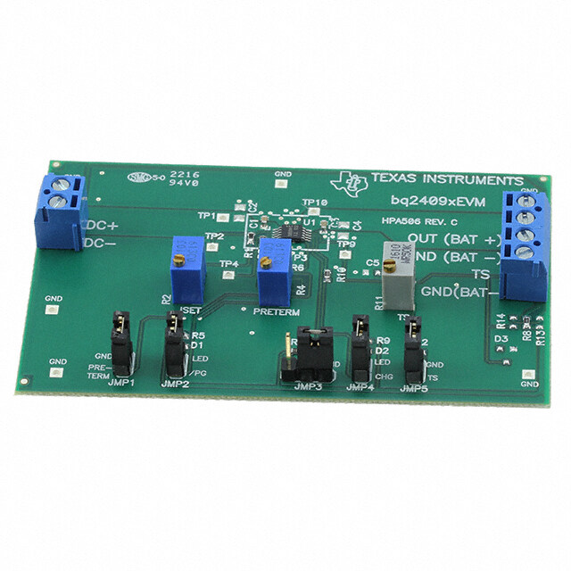
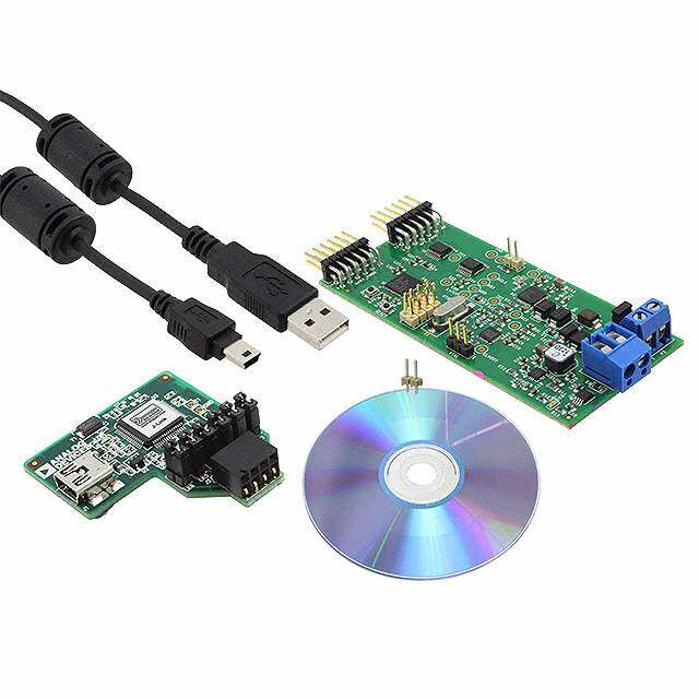
| 产品图片 |
|
| rohs | 符合RoHS无铅 / 符合限制有害物质指令(RoHS)规范要求 |
| 产品系列 | 模拟与数字IC开发工具,数据转换 IC 开发工具,Analog Devices EVAL-CN0216-SDPZCircuits from the Lab™ |
| 数据手册 | |
| 产品型号 | EVAL-CN0216-SDPZ |
| 主要属性 | - |
| 主要用途 | 参考设计,称量台 |
| 产品 | Evaluation Boards |
| 产品种类 | 数据转换 IC 开发工具 |
| 使用的IC/零件 | AD7791,ADA4528-1,ADP3301 |
| 其它名称 | EVALCN0216SDPZ |
| 商标 | Analog Devices |
| 封装 | Bulk |
| 嵌入式 | 否 |
| 工作电源电压 | 6 V |
| 工具用于评估 | AD7791, ADA4528-1 |
| 工厂包装数量 | 1 |
| 所含物品 | 板 |
| 接口类型 | USB |
| 标准包装 | 1 |
| 用于 | EVAL-SDP-CB1Z |
| 类型 | ADC |
| 设计资源 | |
| 辅助属性 | - |


- 商务部:美国ITC正式对集成电路等产品启动337调查
- 曝三星4nm工艺存在良率问题 高通将骁龙8 Gen1或转产台积电
- 太阳诱电将投资9.5亿元在常州建新厂生产MLCC 预计2023年完工
- 英特尔发布欧洲新工厂建设计划 深化IDM 2.0 战略
- 台积电先进制程称霸业界 有大客户加持明年业绩稳了
- 达到5530亿美元!SIA预计今年全球半导体销售额将创下新高
- 英特尔拟将自动驾驶子公司Mobileye上市 估值或超500亿美元
- 三星加码芯片和SET,合并消费电子和移动部门,撤换高东真等 CEO
- 三星电子宣布重大人事变动 还合并消费电子和移动部门
- 海关总署:前11个月进口集成电路产品价值2.52万亿元 增长14.8%

PDF Datasheet 数据手册内容提取
Circuit Note CN-0216 Devices Connected/Referenced Low Power, Buffered, 24-Bit Sigma-Delta Circuits from the Lab™ reference circuits are engineered and AD7791 ADC tested for quick and easy system integration to help solve today’s analog, mixed-signal, and RF design challenges. For more ADA4528-1 Precision, Ultralow Noise, Rail-to-Rail information and/or support, visit www.analog.com/CN0216. Input/Output, Zero-Drift Op Amp High Accuracy anyCAP® 100 mA Low ADP3301 Dropout Linear Regulator Precision Weigh Scale Design Using the AD7791 24-Bit Sigma-Delta ADC with External ADA4528-1 Zero-Drift Amplifiers EVALUATION AND DESIGN SUPPORT Ultralow noise, low offset voltage, and low drift amplifiers are used at the front end for amplification of the low-level signal Circuit Evaluation Boards from the load cell. The circuit yields 15.3 bit noise-free code CN-0216 Circuit Evaluation Board (EVAL-CN0216-SDPZ) resolution for a load cell with a full-scale output of 10 mV. System Demonstration Platform (EVAL-SDP-CB1Z) Design and Integration Files This circuit allows great flexibility in designing a custom low- Schematics, Layout Files, Bill of Materials level signal conditioning front end that gives the user the ability to easily optimize the overall transfer function of the combined CIRCUIT FUNCTION AND BENEFITS sensor-amplifier-converter circuit. The AD7791 maintains good The circuit in Figure 1 is a precision weigh scale signal performance over the complete output data range, from 9.5 Hz conditioning system. It uses the AD7791, a low power buffered to 120 Hz, which allows it to be used in weigh scale applications 24-bit sigma-delta ADC along with two external ADA4528-1 that operate at various low speeds. zero-drift amplifiers. This solution allows for high dc gain with a single supply. +5.0V +5.0V 0.1µF 10µF ADA4528-1 VDD AD7791 100pF SDP BOARD R111.3kΩ REFIN(+) AND 1µF REFIN(–) SUPPORT CIRCUITS C1 3.3µF 100pF DIN RG 33Ω +5.0V 60.4Ω DOUT/RDY LOAD CELL: C2 3.3µF 33Ω TE5D0E5HA- 0H0U0N2T-FL0E7I0GH SENSE+ R211.3kΩ R3 1kΩ 1µF C3 AIN(+) SCCLKS 3333ΩΩ OUT– OUT+ 10µF C5 +5.0V AIN(–) R4 1kΩ 1µF C4 ADA4528-1 SENSE– GND ADP3301-5.0 5.0V VIN IN OUT 10µF 0.1µF IN OUT 0.1µF 4.7µF SD NR ERR GND 10164-001 Figure 1. Weigh Scale System Using the AD7791 (Simplified Schematic, All Connections and Decoupling Not Shown) Rev. 0 Circuits from the Lab™ circuits from Analog Devices have been designed and built by Analog Devices engineers. Standard engineering practices have been employed in the design and construction of each circuit, and their function and performance have been tested and verified in a lab environment at room temperature. However, you are solely responsible for testing the circuit and determining its One Technology Way, P.O. Box 9106, Norwood, MA 02062-9106, U.S.A. suitability and applicability for your use and application. Accordingly, in no event shall Analog Devices be liable for direct, indirect, special, incidental, consequential or punitive damages due to any cause Tel: 781.329.4700 www.analog.com whatsoever connected to the use of any Circuits from the Lab circuits. (Continued on last page) Fax: 781.461.3113 ©2011 Analog Devices, Inc. All rights reserved.
CN-0216 Circuit Note CIRCUIT DESCRIPTION The two ADA4528-1 op amps are configured as the first stage of Figure 2 shows the actual test setup. For testing purposes, a a three op amp instrumentation amplifier. A third op amp 6-wire Tedea-Huntleigh 505H-0002-F070 load cell is used. connected as a difference amplifier would normally be used for Current flowing through a PCB trace produces an IR voltage the second stage, but in the circuit of Figure 1, the differential drop, and with longer traces, this voltage drop can be several input of the AD7791 performs this function. millivolts or more, introducing a considerable error. A 1 inch The gain is equal to 1 + 2R1/RG. Capacitors C1 and C2 are long, 0.005 inch wide trace of 1 oz copper has a resistance of placed in the feedback loops of the op amps and form 4.3 Hz approximately 100 mΩ at room temperature. With a load cutoff frequency low-pass filters with R1 and R2. This limits the current of 10 mA, this can introduce a 1 mV error. amount of noise entering the sigma-delta ADC. C5 in A 6-wire load cell has two sense pins, in addition to the conjunction with R3 and R4 form a differential filter with a excitation, ground, and two output connections. The sense pins cutoff frequency of 8 Hz, which further limits the noise. C3 and are connected to the high side (excitation pin) and low side C4 in conjunction with R3 and R4 form common-mode filters (ground pin) of the Wheatstone bridge. The voltage developed with a cutoff frequency of 159 Hz. across the bridge can be accurately measured regardless of the The ADP3301 low noise regulator powers the AD7791, voltage drop due to wire resistance. In addition, the AD7791 ADA4528-1, and the load cell. In addition to decoupling accepts differential analog inputs and a differential reference as capacitors, a noise reduction capacitor is placed on the regulator well. These two sense pins are connected to the AD7791 output as recommended in the ADP3301 data sheet. It is reference inputs to create a ratiometric configuration that is essential that the regulator is low noise, because any noise on immune to low frequency changes in the power supply the power supply or ground plane introduces noise into the excitation voltage. The ratiometric connection eliminates the system and degrades the circuit performance. need for a precision voltage reference. Unlike a 6-wire load cell, a 4-wire load cell does not have sense pins, and the ADC differential reference pins are connected directly to the excitation voltage and ground. With this connection, there exists a voltage difference between the excitation pin and the reference pin on the ADC due to wire resistance. There will also be a voltage difference on the low side (ground) due to wire resistance. The system will not be completely ratiometric. The Tedea-Huntleigh 2 kg load cell has a sensitivity of 2 mV/V and a full-scale output of 10 mV when the excitation voltage is 5 V. A load cell also has an offset, or TARE, associated with it. In addition, the load cell also has a gain error. Some customers use a DAC to remove or null the TARE. When the AD7791 uses a± 55 VV, orerf e1r0e Vnc pe,- pit.s T dhifef ecrierncutiiat li nan Failgougr ien 1p uamt rpalnifgiee si st heeq uloaal dto c ell 10164-002 Figure 2. Weigh Scale System Setup Using the AD7791 output by a factor of 375 (1 + 2R1/RG), so the full-scale input range referred to the load cell output is 10 V/375 = 27 mV p-p. The 24-bit sigma-delta ADC AD7791 converts the amplified This extra range relative to the 10 mV p-p load cell full-scale signal from the load cell. The AD7791 is configured to operate signal is beneficial as it ensures that the offset and gain error of in the buffered mode to accommodate the impedance of the the load cell do not overload the ADC’s front end. R-C filter network on the analog input pins. The low-level amplitude signal from the load cell is amplified by Figure 3 shows the AD7791’s rms noise for different output data two ADA4528-1 zero-drift amplifiers. A zero-drift amplifier, as rates. This plot shows that the rms noise increases as the output the name suggests, has a close to zero offset voltage drift. The data rate increases. However, the device maintains good noise amplifier continuously self-corrects for any dc errors, making it performance over the complete range of output data rates. as accurate as possible. Besides having low offset voltage and drift, a zero-drift amplfier also exhibits no 1/f noise. This important feature allows precision weigh scale measurement at dc or low frequency. Rev. 0 | Page 2 of 5
Circuit Note CN-0216 100 Therefore, the corresponding noise-free code resolution of the total system is: log (39,557) log (39,557)= 10 =15.3bits 2 log (2) 10 10 V) E (µ Figure 4 shows a plot of the ADC codes for 500 samples OIS (52.6 sec for 9.5 Hz data rate). Note that the peak-to-peak N S spread is about 160 codes. M R 1 0.11 O1U0TPUT DATA RATE 1(H0z0) 1000 10164-003 Figure 3. AD7791 RMS Noise for Different Output Data Rates and a 2.5 V Reference (5 V p-p Input Range), Buffer On The AD7791 rms noise of 1.1 µV for a 9.5 Hz output data rate and a reference of 2.5 V yields the following number of noise- free counts: 5V =688,705 6.6×1.1μV where the factor of 6.6 converts the rms voltage into a peak-to- peak voltage. The corresponding noise-free code resolution is, therefore: log2(688,705)= log1lo0(g6180(82,7)05)=19.5bits 10164-004 Figure 4. Measured Output Code for 500 Samples Showing Note that this represents the performance of the AD7791 the Effects of Noise without the load cell or the input amplifier connected. Figure 5 shows the same data presented in a histogram. Figure 4 The ADA4528-1 has 5.9 nV/√Hz of voltage noise density and, and Figure 5 show the actual (raw) conversions read back from therefore, the input amplifiers and resistors will add noise to the the AD7791. In practice, a digital post filter is typically used in a system. In addition, the load cell itself will add noise. weigh scale system. The additional averaging that is performed In the circuit of Figure 1, a 5 V reference is used, therefore, the in the post filter will further improve the number of noise-free peak-to-peak input range is 10 V. The LSB is, therefore, equal to counts at the expense of a reduced data rate. 10V The resolution of the system in grams can be calculated by 1LSB= =0.596μV 224 2kg =0.05g The 10 mV p-p full-scale signal from the load cell produces a 39,557 3.75 V p-p signal into the ADC, which is approximately 38% of As with any high accuracy circuit, proper layout, grounding, the ADC range. and decoupling techniques must be employed. See Tutorial Seven sets of 500 samples each were taken with the load cell MT-031, Grounding Data Converters and Solving the Mystery of connected (no load). The peak-to-peak code spread for each AGND and DGND and Tutorial MT-101, Decoupling Techniques sample set was calculated, and the seven values averaged to for more details. A complete design support package for this yield a code spread of 159 counts. This corresponds to 159 × circuit note can be found at www.analog.com/CN0216- 0.596 µV = 94.8 µV p-p noise based on a full-scale input to the DesignSupport. ADC of 3.75 V p-p. Therefore, the number of noise-free counts is 3.75V =39,557 94.8μV Rev. 0 | Page 3 of 5
CN-0216 Circuit Note Getting Started Load the evaluation software by placing the CN0216 Evaluation Software disc in the CD drive of the PC. Using My Computer, locate the drive that contains the evaluation software disc and open the Readme file. Follow the instructions contained in the Readme file for installing and using the evaluation software. Functional Block Diagram See Figure 1 of this circuit note for the circuit block diagram, and the PDF file “EVAL-CN0216-SDPZ-SCH” for the circuit schematics. This file is contained in the CN0216 Design Support Package. Setup Connect the 120-pin connector on the EVAL-CN0216-SDPZ circuit board to the connector marked “CON A” on the EVAL-SDP-CB1Z evaluation (SDP) board. Nylon hardware should be used to firmly secure the two boards, using the holes 10164-005 lporaodv icdeeldl t ahte t EhVe AenLd-Cs oNf 0t2h1e6 1-2S0D-PpiZn bcooanrnde. ctors. Connect the Figure 5. Measured Histogram for 500 Samples Showing With power to the supply off, connect a +6 V power supply to the Effects of Noise the pins marked “+6 V” and “GND” on the board. If available, a COMMON VARIATIONS +6 V "wall wart" can be connected to the barrel jack connector on the board and used in place of the +6 V power supply. Other ADCs and circuits suitable for weigh scale applications Connect the USB cable supplied with the SDP board to the USB are discussed in CN-0102 (AD7190), CN-0107 (AD7780), CN- port on the PC. Note: Do not connect the USB cable to the mini 0108 (AD7781), CN-0118 (AD7191), CN-0119 (AD7192), and USB connector on the SDP board at this time. CN-0155 (AD7195). Test The AD7171 is a 16-bit sigma-delta ADC. Apply power to the +6 V supply (or “wall wart”) connected to For a lower power consumption solution, use the ADA4051-2. EVAL-CN0216-SDPZ circuit board. Launch the evaluation The ADA4051-2 is a dual micropower, zero-drift amplifier with software and connect the USB cable from the PC to the USB only 20 µA of supply current per amplifier. mini-connector on the SDP board. The software will be able to CIRCUIT EVALUATION AND TEST communicate to the SDP board if the Analog Devices System This circuit uses the EVAL-CN0216-SDPZ circuit board and Development Platform driver is listed in the Device Manager. the EVAL-SDP-CB1Z system demonstration platform (SDP) Once USB communications are established, the SDP board can evaluation board. The two boards have 120-pin mating now be used to send, receive, and capture serial data from the connectors, allowing for the quick setup and evaluation of the EVAL-CN0216-SDPZ board. circuit’s performance. The EVAL-CN0216-SDPZ board contains Information and details regarding how to use the evaluation the circuit to be evaluated, as described in this note, and the software for data capture can be found in the CN0216 SDP evaluation board is used with the CN-0216 evaluation Evaluation Software Readme file. software to capture the data from the EVAL-CN0216-SDPZ circuit board. Information regarding the SDP board can be found in the SDP User Guide. Equipment Needed Analyzing the Data • PC with a USB port and Windows XP or Windows Vista (32-bit), or Windows 7 (32-bit) At least 500 samples of the ADC output data should be taken. Once the sample set is exported to a spreadsheet program, such • EVAL-CN0216-SDPZ circuit evaluation board as Excel, the samples can be analyzed. The standard deviation of • EVAL-SDP-CB1Z SDP evaluation board the samples is approximately equal to the rms noise, assuming a Gaussian noise distribution. The peak-to-peak noise is • CN0216 evaluation software approximately equal to the rms value multiplied by 6.6. • Tedea-Huntleigh 505H-0002-F070 load cell or equivalent The peak-to-peak noise can also be taken directly from the • Power supply: +6 V, or +6 V “wall wart” sample set by simply taking the difference between the largest and smallest sample. In practice, the results obtained using this Rev. 0 | Page 4 of 5
Circuit Note CN-0216 method were approximately the same as the value obtained by CN-0102 Circuit Note, Precision Weigh Scale Design Using the multiplying the rms value by 6.6. AD7190 24-Bit Sigma-Delta ADC with Internal PGA, Analog Devices. The values obtained from the sample set are in LSBs, so they must be converted into voltage, where 1 LSB = 0.596 µV for a CN-0107 Circuit Note, Weigh Scale Design Using the AD7780 5 V reference. 24-Bit Sigma-Delta ADC with Internal PGA, Analog Devices. If desired, the results of several sample sets can be averaged to get a more accurate measurement. CN-0108 Circuit Note, Weigh Scale Design Using the AD7781 20-Bit Sigma-Delta ADC with Internal PGA, Analog Noise-free code resolution is calculated from the peak-to-peak Devices. noise as described previously in this circuit note. CN-0118 Circuit Note, Precision Weigh Scale Design Using the LEARN MORE AD7191 24-Bit Sigma-Delta ADC with Internal PGA, Kester, Walt. 1999. Sensor Signal Conditioning. Section 2. Analog Devices. Analog Devices. CN-0119 Circuit Note, Precision Weigh Scale Design Using the Kester, Walt. 1999. Sensor Signal Conditioning. Section 3. AD7192 24-Bit Sigma-Delta ADC with Internal PGA, Analog Devices. Analog Devices. Kester, Walt. 1999. Sensor Signal Conditioning. Section 4. CN-0155 Circuit Note, Precision Weigh Scale Design Using a 24- Analog Devices. Bit Sigma-Delta ADC with Internal PGA and AC Excitation, MT-004 Tutorial, The Good, the Bad, and the Ugly Aspects of Analog Devices. ADC Input Noise—Is No Noise Good Noise? Analog Devices. Data Sheets and Evaluation Boards MT-022 Tutorial, ADC Architectures III: Sigma-Delta ADC AD7791 Data Sheet Basics, Analog Devices. ADA4528-1 Data Sheet MT-023 Tutorial, ADC Architectures IV: Sigma-Delta ADC ADP3301 Data Sheet Advanced Concepts and Applications, Analog Devices. CN-0216 Circuit Evaluation Board (EVAL-CN0216-SDPZ) MT-031 Tutorial, Grounding Data Converters and Solving the Mystery of "AGND" and "DGND", Analog Devices. System Demonstration Platform (EVAL-SDP-CB1Z) MT-063 Tutorial, Basic Three Op Amp In-Amp Configuration, Analog Devices. MT-101 Tutorial, Decoupling Techniques, Analog Devices. REVISION HISTORY Wong, Vicky, AN-1114 Application Note, Lowest Noise Zero- 9/11—Revision 0: Initial Version Drift Amplifier Has 5.6 nV/√Hz Voltage Noise Density, Analog Devices. (Continued from first page) Circuits from the Lab circuits are intended only for use with Analog Devices products and are the intellectual property of Analog Devices or its licensors. While you may use the Circuits from the Lab circuits in the design of your product, no other license is granted by implication or otherwise under any patents or other intellectual property by application or use of the Circuits from the Lab circuits. Information furnished by Analog Devices is believed to be accurate and reliable. However, "Circuits from the Lab" are supplied "as is" and without warranties of any kind, express, implied, or statutory including, but not limited to, any implied warranty of merchantability, noninfringement or fitness for a particular purpose and no responsibility is assumed by Analog Devices for their use, nor for any infringements of patents or other rights of third parties that may result from their use. Analog Devices reserves the right to change any Circuits from the Lab circuits at any time without notice but is under no obligation to do so. ©2011 Analog Devices, Inc. All rights reserved. Trademarks and registered trademarks are the property of their respective owners. CN10164-0-9/11(0) Rev. 0 | Page 5 of 5