ICGOO在线商城 > 开发板,套件,编程器 > 评估和演示板和套件 > EVAL-ADE7758ZEB
 Datasheet下载
- 型号: EVAL-ADE7758ZEB
- 制造商: Analog
- 库位|库存: xxxx|xxxx
- 要求:
| 数量阶梯 | 香港交货 | 国内含税 |
| +xxxx | $xxxx | ¥xxxx |
查看当月历史价格
查看今年历史价格
EVAL-ADE7758ZEB产品简介:
ICGOO电子元器件商城为您提供EVAL-ADE7758ZEB由Analog设计生产,在icgoo商城现货销售,并且可以通过原厂、代理商等渠道进行代购。 EVAL-ADE7758ZEB价格参考。AnalogEVAL-ADE7758ZEB封装/规格:评估和演示板和套件, ADE7758 Energy/Power Meter Power Management Evaluation Board。您可以下载EVAL-ADE7758ZEB参考资料、Datasheet数据手册功能说明书,资料中有EVAL-ADE7758ZEB 详细功能的应用电路图电压和使用方法及教程。
EVAL-ADE7758ZEB是Analog Devices Inc.推出的一款评估板,专用于评估ADE7758电能计量IC的性能。该评估板主要应用于电力监测与管理系统中,适用于需要高精度电量测量的场景。

其典型应用场景包括智能电表、工业自动化系统中的电力质量分析、能源管理系统以及家用电器的能耗监控等。通过使用EVAL-ADE7758ZEB,工程师可以快速验证ADE7758芯片在有功功率、无功功率、电压、电流及频率等方面的测量精度和稳定性,从而加速产品开发进程。

此外,该评估板也支持对谐波分析功能的测试,这对于提升电网中非线性负载带来的电力质量问题具有重要意义。因此,EVAL-ADE7758ZEB广泛应用于电力电子、智能电网及相关研发领域。
| 参数 | 数值 |
| 产品目录 | 编程器,开发系统半导体 |
| 描述 | BOARD EVAL FOR AD7758数据转换 IC 开发工具 EVAL-ADE7758ZEB |
| 产品分类 | |
| 品牌 | Analog Devices |
| 产品手册 | |
| 产品图片 |
|
| rohs | 符合RoHS无铅 / 符合限制有害物质指令(RoHS)规范要求 |
| 产品系列 | 数据转换 IC 开发工具,Analog Devices EVAL-ADE7758ZEB- |
| 数据手册 | |
| 产品型号 | EVAL-ADE7758ZEB |
| 主要属性 | - |
| 主要用途 | 电源管理,电度表/功率表 |
| 产品 | Evaluation Boards |
| 产品种类 | 数据转换 IC 开发工具 |
| 使用的IC/零件 | ADE7758 |
| 其它名称 | EVALADE7758ZEB |
| 商标 | Analog Devices |
| 封装 | Bulk |
| 嵌入式 | 否 |
| 工作电源电压 | 5 V |
| 工具用于评估 | ADE7758 |
| 工厂包装数量 | 1 |
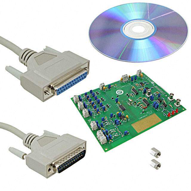
| 所含物品 | 板,软件 |
| 接口类型 | Parallel |
| 标准包装 | 1 |
| 类型 | ADC |
| 系列 | ADE7758 |
| 辅助属性 | - |


- 商务部:美国ITC正式对集成电路等产品启动337调查
- 曝三星4nm工艺存在良率问题 高通将骁龙8 Gen1或转产台积电
- 太阳诱电将投资9.5亿元在常州建新厂生产MLCC 预计2023年完工
- 英特尔发布欧洲新工厂建设计划 深化IDM 2.0 战略
- 台积电先进制程称霸业界 有大客户加持明年业绩稳了
- 达到5530亿美元!SIA预计今年全球半导体销售额将创下新高
- 英特尔拟将自动驾驶子公司Mobileye上市 估值或超500亿美元
- 三星加码芯片和SET,合并消费电子和移动部门,撤换高东真等 CEO
- 三星电子宣布重大人事变动 还合并消费电子和移动部门
- 海关总署:前11个月进口集成电路产品价值2.52万亿元 增长14.8%


PDF Datasheet 数据手册内容提取
PRELIMINARY TECHNICAL DATA a Evaluation Board Documentation ADE7758 Energy metering IC Preliminary Technical Data EVAL-ADE7758EB FEATURES WindowsTM based software is provided with the evaluation Evaluation Board is designed to be used together with board which allows it to be quickly configured as an energy accompanying software to implement a fully functional meter. Three-Phase Energy Meter (Watt-Hour Meter). The ADE7758 evaluation board and this documentation, Easy connection of various external transducers via together with the ADE7758 data sheet provide a complete screw terminals. evaluation platform for the ADE7758. Easy modification of signal conditioning components The evaluation board has been designed so that the ADE7758 using PCB sockets. can be evaluated in the end application, i.e., Watt-Hour LED indicators on logic outputs CF, VARCF, and Meter. Using the appropriate transducers on the current IRQ. channel (e.g., CT) the evaluation board can be connected to Optically isolated data output connection to PC parallel port. a test bench or high voltage (240V rms) test circuit. On-board Optically isolated frequency output (CF) to BNC. resistor dividers networks provide the attenuation for the line External Reference option available for on-chip voltages. This application note also describes how the current reference evaluation. transducers should be connected for the best performance. GENERAL DESCRIPTION The evaluation board requires two external 5V power sup- The ADE7758 is high accuracy electrical active power plies (one is required for isolation purposes) and the appro- measurement ICs for three-phase applications with a pulse priate current transducers. output. This output is intended to be used for calibration purposes. The ADE7758 incorporate ADCs, reference cir- cuitry, and all the signal processing required to perform energy measurement. The ADE7758 provides per phase Active, Reactive, and Apparent Energy information, RMS values, and temperature measurement via a serial interface. This documentation describes the ADE7758 evaluation kit Hardware and Soft- ware functionality. The evaluation board (watt-hour meter) is configured via the parallel port of a PC. The data interface between the evaluation board and the PC is fully isolated. FUNCTIONAL BLOCK DIAGRAM AVDDAGND DVDD DGND +5V V+ V- IAP DOUT IAN SCLK 74HC08 DIN IIBBNP NeFtiwlteorrk ADE7758 CS RESET Connector to ICP PC Parallel ICN Port VN 74HC08 VCP Filter Network GND & VBP Attenuation CF VARCF IRQ BNC VAP Isolated Frequency CF GND output Optional ExternalAD780 BNC 2.5V Reference External Clock in BNC VARCF PROTOTYPE AREA REV. PrB 08/03 Information furnished by Analog Devices is believed to be accurate and reliable. However, no responsibility is assumed by Analog Devices for its use, nor for any infringements of patents or other rights of third parties which may result from its use. No license is granted by implication or One Technology Way, P.O. Box 9106, Norwood. MA 02062-9106, U.S.A. otherwise under any patent or patent rights of Analog Devices. Tel: 617/329-4700 Fax: 617/326-8703
PRELIMINARY TECHNICAL DATA EVAL-ADE7758EB ANALOG INPUTS (P4, P5, P6, P7, P8 AND P11) Using a CT as the current transducer Voltage and current signals are connected at the screw Figure 2 shows how a CT can be used as a current transducer terminals P4-P6 and P7-P8 and P11 respectively. All analog in one phase of a 3-phase 4-wire distribution system (Phase input signals are filtered using the on-board anti-alias filters A). In a three phase distribution system Phase A, Phase B and before being presented to the analog inputs of the ADE7758. Phase C are nominally 120° phase difference to each other. The default component values which are shipped with the Each phase usually requires a connection of this type for evaluation board are the recommended values to be used with current sensing. the ADE7758. The user can easily change these components, however this is not recommended unless the user is familiar with sigma-delta converters and also the criteria used for ADE7758 selecting the component values for the analog input filters - I max = 40A SH1A JP4 JP5 See ADE7758 datasheet. CT 8Ω TP2 1:1800 IAP Current sense inputs (P4, P5 and P6) JP2 100Ω 1kΩ 33nF P4, P5 and P6 are two-way connection blocks which allow JP25 JP6 355mV AtcooD nbEnee7 c7ct5oo8rn 'nsP e4ccu teardrne dnt ott hicneu pfruirltetsen rtoi nft grp annhesadtsweu ocAerkr,s .Bw F haiicgnhud r eiCs 1 p rresoshvpoiedwcetsdi v teohlnye Phase A SH81ΩB J1P001Ω 1kΩ 33TnFP4 IArNms the evaluation board. Full Scale The resistors SH1A, SH2A, SH1B, SH2B, SH1C and differential input = 0.5V SH2C are by default not populated. They are intended to be used as burden resistors when CTs are used as the current transducers—see using a CT as a the current transducer. Figure 2 — CT connection to Current Channel The RC networks R9/C5, R7/C8, R15/C9, R13/C12, R21/ C13, R19/C16 are used to provide phase compensation when The CT secondary current is converted to a voltage by using a Current Transformer is being used as the current transducer a burden resistance across the secondary winding outputs. with the ADE7758—see using a Current Transformer as the Care should be taken when using a CT as the current current transducer. These RC networks are easily disabled by transducer. If the secondary is left open, i.e., no burden is placing JP4, JP1, JP10, JP7, JP16 & JP13 and removing C5, connected, a large voltage could be present at the secondary C8, C9, C12, C13 and C16 (socketed). outputs. This can cause an electrical shock hazard and The RC networks R10/C6, R8/C7, R16/C10, R14/C11, potentially damage electronic components. R22/C14 and R20/C15 are the anti-alias filters which are required by the on-chip ADCs. The default corner frequency Warning! for these LPFs (Low Pass Filters) is selected as 4.8kHz (1kΩ Using a CT without a burden resistor & 33nF). These filters can easily be adjusted by replacing the can lead to electrical shock. components on the evaluation board. However before adjust- ing the component values the user should first review the The anti-alias filters should be enabled by opening jumpers ADE7758 datasheet. JP5, JP6, JP11, JP12, JP17 and JP18—see Figure 2. Most CTs will have an associated phase shift of between 0.1° ADE7758 and 1° at 50Hz/60Hz. This phase shift or phase error can lead SH1A to significant energy measurement errors, especially at low JP4 JP5 R11 TP2 power factors. However this phase error can be corrected by R9 R10 P4 1 IAP writing to the Phase Calibration registers (APHCAL, JP2 100Ω C5 1kΩ C6 BPHCAL and CPHCAL) in the ADE7758. The software JP1 33nF JP6 33nF supplied with the ADE7758 evaluation board allows user TP4 R7 R8 adjustment of the Phase Calibration register. See the Evalu- P4 2 IAN SRH61B J1P030Ω C338nF 1kΩ C337nF aFtoiorn tShoisft weaxrae mDpelsec,r ipntiootni cfeo r thmaotr et hine fomrmaxaitmiounm. analog input range on the Current channel is set to 0.5V. When using the ADE7758, the Gain for Current channel has been set to 1. The maximum analog input range and gain are set via the Gain register (GAIN)—see the ADE7758 data Figure 1 — Current Channel on the ADE7758 evaluation sheet. The evaluation software allows the user to configure the board current channel gain. This means that the maximum peak differential signal on the current channel is 0.5V. –2– REV. PrB 08/03
PRELIMINARY TECHNICAL DATA EVAL-ADE7758EB Voltage sense inputs (P7, P8 and P11) The voltage inputs connections on the ADE7758 evaluation board can be directly connected to the line voltage sources. The line voltages are attenuated using a simple resistor divider network before it is presented to the ADE7758. The attenuation network on the voltage channels is designed such that the corner frequency (3dB frequency) of the network matches that of the RC (anti-aliasing) filters on the current channels inputs. This is important, because if they do not match there will be large errors at low power factors. The Serial interface along with the digital parameters of the ADE7758 enable a fully software calibration procedure. In this case, the voltage attenuation networks are made up of R48, R49 and R47 for Phase A, R45, R46 and R44 for Phase B and R41, R42 and R43 for Phase C. Figure 3 shows a typical connection for the line voltage when using fixed resistors. ADE7758 JP27 P8 2 R40 JP32 TP13 VN JP28 1kΩ C1 33nF JP25 P7 1 R48 R49 TP17 VAP Neutral Phase A 100 - 25J0P V3 r8ms 499kAΩtNteentwuaotrikon499kΩ C334nF1Rk4Ω7 JP49 2rm00s - 300 mV Figure 3 — Phase A Voltage Channel attenuation network using Fixed resistors The attenuation networks can be easily modified by the user to accommodate any input signal level. However the value of R43, R44 and R47 (1kΩ) should not be altered as the phase response of Voltage channels should match that of the current channels. The maximum signal level permissible at VAP, VBP and VCP is 0.5V peak for the ADE7758. Although the ADE7758 analog inputs can withstand ±6V without risk of permanent damage, the signal range should not exceed ±0.5V with respect to AGND for the ADE7758 for specified operation. Note that the analog input VN is connected to AGND via the anti-alias filter R40/C1 using JP28. Jumper JP27 should be left open. REV. PrB 08/03 –3–
PRELIMINARY TECHNICAL DATA EVAL-ADE7758EB TABLE II : JUMPER SETTINGS JUMPER OPTION DESCRIPTION JP1-JP7-JP13 Closed This will short out R7, R13 and R19 respectively. The effect is to disable the phase compensation filter on the analog inputs IAN, IBN and ICN respectively. Default Closed. JP2-JP8-JP14 Closed This will connect the analog input IAP, IBP and ICP respectively to ground. Default Open. JP3-JP9-JP15 Closed This will connect the analog input IAN, IBN and ICN respectively to ground. Default Open. JP4-JP10-JP16 Closed This will short out R9, R15 and R21 respectively. The effect is to disable the phase compensation filter (for Current transformers) on the analog inputs IAN, IBN and ICN respectively. Default Closed. JP5-JP11-JP17 Closed This will short out R10, R16 and R22 respectively. The effect is to disable the anti-alias filter on the analog inputs IAP, IBP and ICP respectively. Default Open. Open Enable the anti-alias filter on IAP, IBP and ICP respectively. JP6-JP12-JP18 Closed This will short out R8, R14 and R20 respectively. The effect is to disable the anti-alias filter on the analog inputs IAN, IBN and ICN respectively. Default Open. Open Enable the anti-alias filter on IAN, IBN and ICN respectively. JP19 Closed This will connect the Analog and Digital ground planes of the PCB. Default Closed. JP20 Closed This will connect an external reference 2.5V (AD780) to the ADE7754/8 Open This will enable the ADE7758 on-chip reference. JP21 Closed This connects the DVDD and +5V (buffers) supply for the evaluation board together. Default Closed. JP22 Closed This connects the AVDD and DVDD supply for the evaluation board together. Default Closed. JP23-JP24-JP25 Closed This will short the attenuation network on the voltage channels. Default Open JP26 Closed This will connect the optical isolator ground to the evaluation board ground (DGND). If full isolation between the evaluation board and PC is required, this jumper should be left open JP27 Closed This will short out R40. The effect is to disable the anti-alias filter on the analog input VN. Default Open JP28 Closed This will connect the analog input VN to ground. Default Closed. JP29-JP35-JP38 Closed This will connect the analog inputs VCP, VBP and VAP to ground respectively. Default Open- JP47-JP48-JP49 Closed This will short out disconnect Analog input VCP, VBP and VAP respectively from the ADE7758. Default Closed JP30 Closed This connects the buffered logic output VARCF to the LED CR1. Default Open. JP31 Closed This connects the buffered logic output VARCF to BNC J1 connector via an optical isolator. Default Open. JP32 Closed This will short out disconnect Analog input VN from the ADE7758. Default Closed JP43 A This connects the buffered logic output CF to BNC J3 connector via an optical isolator. B This connects the buffered logic output CF to the LED CR2. JP44 A This connects the buffered logic output IRQ to the parallel port. B This connects the uffered logic output IRQ the LED CR3. JP46 N/A This jumper is not used for the ADE7758, the setting does not matter. –4– REV. PrB 08/03
PRELIMINARY TECHNICAL DATA EVAL-ADE7758EB SETTING UP THE EVALUATION BOARD AS AN The evaluation board is connected to the PC parallel port ENERGY METER using the cable supplied. The cable length should not Figure 4 shows a typical set up for the ADE7758 evaluation exceed 6 feets (2 meters) or the serial communication board. In this example a kWh meter for a 4 wire, three phase between the PC and the evaluation board may become distribution system is shown. Current Transformers are used unpredictable and error prone. to sense phases' current and are connected as shown in Figure When the evaluation board has been powered up and is 4. For a more detailed description on how to use a CT as a connected to the PC, the supplied software can be current transducer see the Current Sense Inputs section of this launched. The software will automatically start in default documentation. The line voltage is connected directly to the mode. The next section describes the ADE7758 evalu- evaluation board as shown. Note JP23, JP24 and JP25 should ation software in detail and how it can be installed and be left open to ensure that the attenuation networks are not uninstalled. bypassed. Also note the use of two power supplies. The second power supply is used to power the optical isolation. With JP26 left open, this will ensure that there is no electrical connection between the high voltage test circuit and the frequencies outputs. The power supplies should have floating voltage outputs. Setting up the evaluation board for the ADE7758 The configuration of the jumpers on the ADE7758 evaluation board for operation with the ADE7758 is detailed in Figure 4. - - 5.000 V 5.000 V + + D D (cid:7)(cid:12)(cid:10)(cid:13)(cid:6)(cid:14)(cid:15) D N (cid:1)(cid:2)(cid:3)(cid:4)(cid:5)(cid:6) DV DG V+ V- (cid:27)(cid:7)(cid:19)(cid:28)(cid:14)(cid:29)(cid:14)(cid:15)(cid:9)(cid:30)(cid:1)(cid:21)(cid:31) (cid:7)(cid:12)(cid:10)(cid:13)(cid:6)(cid:14)(cid:16) (cid:7)(cid:19)! (cid:7) (cid:27)(cid:7) !(cid:14)(cid:29)(cid:14)(cid:30)(cid:7)(cid:21)(cid:20) (cid:27)(cid:7) (cid:19)(cid:14)(cid:29)(cid:14)(cid:15)(cid:9)(cid:30)(cid:1)(cid:21)(cid:31) (cid:27)(cid:7) (cid:14)(cid:29)(cid:14)(cid:15)(cid:9)(cid:30)(cid:1)(cid:21)(cid:31) (cid:7)(cid:12)(cid:10)(cid:13)(cid:6)(cid:14)(cid:17) (cid:9) (cid:7)(cid:26) (cid:24)(cid:17) IAP JP1 = CLOSED (cid:20)(cid:21)(cid:22)(cid:23) CT SSHH12AA IAN JJJJJPPPPP42356 ===== COOOOLPPPPOEEEESNNNNED (cid:7)(cid:25) IBP JP7 = CLOSED SH1B JP8 = OPEN CT JJPP190 = = O CPLEONSED SH2B IBN JJPP1112 == OOPPEENN P9 = RIGHT (cid:7)(cid:8) ICP JP13 = CLOSED To PC SH1C JP14 = OPEN CT JJPP1156 == OCLPOESNED Parallel Port SH2C ICN JP17 = OPEN JP18 = OPEN (cid:7)(cid:18) JP27 R40 JP32 VN JP27 = OPEN JP28 = CLOSED JP28 C1 JP32 = CLOSED JP23 R41 R42 C2 JJPP2239 == OOPPEENN JP47 = CLOSED (cid:7)(cid:19)(cid:19) JP29 R43 JP47VCP R43 = 1kΩ JP24 R45 R46 C3 JJPP2345 == OOPPEENN JP48 = CLOSED (cid:7)" JP35 R44 JP48VBP R44 = 1kΩ JP25 R48 R49 C4 JP25 = OPEN JP38 = OPEN (cid:9)(cid:2)(cid:10)(cid:11) JP38 R47 JP49VAP JRP4479 = = 1 CkΩLOSED (cid:20)(cid:21)(cid:22)(cid:23)(cid:24)(cid:17)(cid:9) Figure 4 - Typical set up for the ADE7754-ADE7758 evaluation board REV. PrB 08/03 –5–
PRELIMINARY TECHNICAL DATA EVAL-ADE7758EB ADE7758 EVALUATION SOFTWARE Default Mode The ADE7758 evaluation board is supported by Windows When the software is launched, the default screen shows the based software which will allows the user to access all the window, or mode, options. The user has the choice in functionality of the ADE7758. The software is designed to different modes of operation: Active Energy, Reactive En- communicate with the ADE7758 evaluation board via the ergy, Apparent Energy Measurements, Voltage channels, parallel port of the PC. Current Channels, Power Quality, Temperature and Inter- Installing the ADE7758 Software rupt. Each mode gives a view of the functionality of the The ADE7758 Software is supplied on one CD-ROM. The ADE7758 and access to the relevent registers in the datapath. minimum requirements for the PC are Pentium II 233MHz, This software should be used in conjunction with the ADE7758 32 MB RAM, 10MB free HD space and at least one PS/2 or datasheet. ECP parallel port . To install the software place the CD- ROM in the CDROM reader and double click "setup.exe". This will launch the set up program which will automatically install all the software components including the uninstall program and create the required directories. When the set up program has finished installing the "EvalADE7758" pro- gram the user will be prompted to install the National Instruments run-time engine. This software was developed using National Instruments LabView software and the run- time engine is required in order to run the "ADE7758Eval" program. Follow the on-screen instructions to complete the installation. You will need to reboot your computer to complete the installation. To launch the software simply go to the Start—>Programs—>EvalADE7758 menu and click on "EvalADE7758". Uninstalling the ADE7758 Evaluation Software Both the "EvalADE7758" program and the NI run-time engine are easily uninstalled by using the Add/Remove Programs facility in the control panel. Simply select the program to uninstall and click the Add/Remove button. When installing a new version of the ADE7758 evaluation software, the previous version should be uninstalled. Figure 6 — Default ADE7758 Mode Selection Window Active Energy Measurement In this mode, all the parameters needed for the measurement of the Active Energy are shown in one window - see Figure 7. Figure 5 — Uninstalling the ADE7758 Eval Software Figure 7 - Active Energy Measurement Window –6– REV. PrB 08/03
PRELIMINARY TECHNICAL DATA EVAL-ADE7758EB The different modes, configuration and register values for The ADE7758 can be reset to its default configuration by the Active Energy Measurement can be selected in this pushing the reset button. window. All configuration registers are written or read to the ADE7758 when pushing the Write Configuration or Read Configuration buttons. The Active Energy and Line Active Energy registers are available by pressing the Read Energy Registers button. The Read Waveform button will launch where the current, voltage and multiplier waveforms are viewable by phase. The ADE7758 can be reset to its default configuration by pushing the reset button. Apparent Energy Measurement In this mode, all the parameters needed for the measurement of the Apparent Energy are presented in one window - see Figure 8. Figure 9 - Reactive Energy Measurement Window Read Energy Registers This window shows all of the energy registers in the ADE7758. There are several options for viewing the contents of the registers. The per phase energies are shown in the top three rows of energy displays. The sum of the three phases for active, apparent and reactive are shown in the bottom row of displays - see Figure 10. The Active, Apparent and Reactive Energy registers can be read separately by pressing the small read buttons. The toggle switch sets the program to read the line accumulation registers or the regular accumulation registers for Active, Apparent or Reactive energy. Additionally, all of the regis- ters can be read simultaneously by using the larger read Figure 8 - Apparent Energy Measurement Window buttons at the top. The configuration registers are written or The different modes, configuration and registers values for read to the ADE7758 by pushing the Write Configuration or the Apparent Energy Measurement can be selected in this Read Configuration buttons. window. All configuration registers are written or read to the ADE7758 when pushing the Write Configuration or Read Configuration buttons. The Apparent Energy and Line Apparent Energy registers are available by pushing the Read Energy Registers button. The Read Waveform button will launch where the current, voltage and multiplier waveforms are viewable by phase. The ADE7758 can be reset to its default configuration by pushing the reset button. Reactive Energy Measurement In this mode, all the parameters needed for the measurement of the Apparent Energy are presented in one window - see Figure 9. The different modes, configuration and register values for the Reactive Energy Measurement can be selected in this window. All configuration registers are written or read to the ADE7758 when pushing the Write Configuration or Read Configuration buttons. The Active Energy and Line Active Energy registers are available by pressing the Read Energy Registers button. The Read Waveform button will launch where the current, voltage and multiplier waveforms are Figure 10- Read Energy Registeres Window viewable by phase. REV. PrB 08/03 –7–
PRELIMINARY TECHNICAL DATA EVAL-ADE7758EB Current Channels Voltage Channels In this mode, all the parameters needed for the measurement In this mode, all the parameters needed for the measurement of the Current channels are presented in one window - see of the Voltage channels are presented in one window - see Figure 12. Figure 11. Figure 12 - Current Channels Window Figure 11 — Voltage Channels Window The register values and information available for the Current Channels can be viewed in this window. All configuration The register values and information available for the Voltage registers are written or read by pushing the Write Configu- Channels can be viewed in this window. All configuration ration or Read Configuration buttons. The Current RMS and registers are written or read to the ADE7758 by pushing the Peak interrupts information are available by pushing the Write Configuration or Read Configuration buttons. To get appropriate buttons. the Voltage RMS, the "Read RMS value" should be de- pressed. Pressing the "Read Frequency" button displays the The Current Channel window gives also access to the line period or the line frequency for the selected phase waveform sampling data by pressing the Read Wavform depending on the toggle switch setting. SAG, Peak and button. Zero-crossing Time-out interrupts information is available The ADE7758 can be reset to its default configuration by by pushing the "Read Events" button. pushing the reset button. The Voltage Channel window gives also access to the Waveform Samples Window waveform sampling data by pressing the Read Waveform The Waveform sample window is available from the energy button. measurement, voltage or current channel windows. This The ADE7758 can be reset to its default configuration by screen allows the user to read the waveform samples register. pushing the reset button. The available waveforms in the ADE7758 include: voltage, current, active power, reactive power, and apparent power. Pressing the Exit button will return the user to the previous window. Figure 11 — Voltage Channels Window –8– REV. PrB 08/03
PRELIMINARY TECHNICAL DATA EVAL-ADE7758EB Interrupts the phase difference at the input to the Current channel is now This window gives access to the Interrupt Mask and STA- 59.89° lag instead of 60° lag. Determining whether the error TUS registers of the ADE7758 - see Figure 14. For details is a lead or lag can also be figured intuitively from the on how to use the Interrupt and Mask registers, refer to the frequency output. Figure 14 shows how the output frequency ADE7758 datasheet. varies with phase (cos{φ}). Since the output frequency B (1.83817Hz) at the PF=0.5 lag setting in the example is actually greater than A/2 (1.833105Hz), this means the phase error between the current channel and the voltage channel was actually less than 60°. This means there was additional lead in the current channel due to the CT. CF (Hz) Frequency B > A/2 PF=1 Phase difference < 60(cid:1) lag PF>0.5 PF=0.5 PF<0.5 PF=0 360(cid:1) 60(cid:1) Phase lag Figure 14—CF Frequency Vs Phase(PF) Figure 14 - Interrupts Window Using the Phase Calibration to correct small (<0.5°) external phase errors Measuring CT Phase Errors using the ADE7758 From the previous example it is seen that the CT introduced The ADE7758 itself can be used to measure a CT (and a phase lead in the current channel of 0.091° . Therefore external components) phase error during calibration. The instead of 60° phase difference between the current channel assumption is that the ADE7758 has no internal phase error and the voltage channel, it is actually 59.89°. In order to (APHCAL = BPHCAL = CPHCAL = 00 hex) and the error bring the phase difference back to 60°, the phase compensa- due to external components is small (<0.5°). The procedure tion circuit in the voltage channel is used to introduce an is based on a two point measurement, at PF=1 and PF = 0.5 extra lead of 0.091°. This is achieved by reducing the amount (lag). The PF is set up using the test bench source and this of time delay in the voltage channel. source must be very accurate. The ADE7758 should be configured for Active Energy measurement mode. The maximum time delay adjustment in the voltage channel An Active Energy measurement is first made with PF=1 is ±75.6µs with a CLKIN of 10MHz. The PHCAL registers (measurement A). A second Active Energy measurement are signed 2's complement 7 bit registers. Each LSB is should be made at PF=0.5 (measurement B). The frequency equivalent to 1.2µs. In this example the line frequency is output CF can be used for this measurement. Using the 50Hz. This means each LSB is equivalent to (360° x 1.2µs formula shown below the phase error is easily calculated: x 50) = 0.022°. To introduce a lead of 0.091° the delay in the voltage channel must be reduced. This is achieved by writing B−A -4 (1Ch) or +0.088° to the PHCAL register. Phase Error (°)=Tan−1A ⋅ 32 Correcting large external phase errors 2 In this example the phase correction range at 50Hz is only approximately ±1.3°. However it is best to only use the For example, using the frequency output CF to measure PHCAL register for small phase corrections, i.e., <0.5°. If power, a frequency of 3.66621Hz is recorded for a PF=1. larger corrections are required the larger part of the correc- The PF is then set to 0.5 lag and a measurement of tion can be made using external passive component. For 1.83817Hz is obtained. Using the formula above the phase example the resistors in the anti-alias filter can be modified error on Channel 1 is calculated as: to shift the corner frequency of the filter so as to introduce Phase Error (°)=Tan−11.83817−3.666212 =+0.0991° m1koΩre aonrd le3s3sn Fla gi.s T0h.5e6 °la ga t th5r0oHugz.h Fthinee aandtij-uasltimase nfitlste rcsa nw ibthe 3.66621 ⋅ 3 made with the PHCAL register. Note that typically CT phase 2 shift will not vary significantly from part to part. If a CT phase shift is 1°, then the part to part variation should only be The formula will also give the correct sign for the phase about ±0.1°. Therefore the bulk of the phase shift (1°) can be error. In this example the phase error is calculated as +0.091° canceled with fixed component values at design. The remain- at the input to the Current channel of ADE7758. This means ing small adjustments can be made in production using the that the CT has introduced a phase lead of 0.091°. Therefore PHCAL registers. REV. PrB 08/03 –9–
PRELIMINARY TECHNICAL DATA EVAL-ADE7758EB Evaluation board BOM Designator Value Description R4, R24, R26, R29-R31 10kΩ, 5%, ¼W Resistor, no special requirements R5, R7, R9, R13, R15, 100Ω, 5%, ¼W Resistor, no special requirements R19, R21, R32-R36, R50-51 R6, R11-12, R17-18, 51Ω, 5%, ¼W Not placed unless external clock is being used R23, R52 R8, R10, R14, R16, R20, 1kΩ, 0.1%, ¼W ±15 ppm/°C Resistor, good tolerance, used as part of the analog filter R22, R40, R43-44, R47 network.These resistors are not soldered, but are plugged into PCB pin sockets for easy modification by the customer. Low drift WELWYN RC55 Series, FARNELL part no. 339-179 R25 10Ω, 5%, ¼W Resistor, no special requirements R38-39 20Ω, 5%, ¼W Resistor, no special requirements R41-42, R45-46, R48-49 499kΩ, 0.1%, ¼W Pin socketed, ±15 ppm/°C Low drift, WELWYN RC55 Series. Farnell part no. 338-484 R53-56, R61, R63-68 820Ω, 5%, ¼W Resistor, no special requirements R69 0Ω, 10%, ¼W C1-16 33nF, 10%, 50 volt X7R Capacitor, part of the filter network. These resistors are not soldered, but are plugged into PCB mount sockets for easy modifica- tion by the customer. SR15 series AVX-KYOCERNA, FARNELL part no. 108-948C5, C17 220pF PANASONIC ECQ-P1H221JZ C18-23 10uF, Tantalium Power supply decoupling capacitors, 10%, 16V C25, C39 22pF, ceramic Gate oscillator load capacitors, FARNELL part no. 108-927 C24, C26-34, C37-38 100nF, 25V Power supply decoupling capacitors, 10%, X7R type, AVX- KYOCERNA, FARNELL part no. 108-950 C11, C21, C50, C51, CR1-3 LED Low current, Red, FARNELL part no. 637-087 CR4 Diode 1N4001, Motorola J1-3 BNC connector Straight square, 1.3mm holes, 10.2mm x 10.2mm FARNELL part no. 149-453 JP1-29, JP32, JP35, JP38, 2 Pin header 2-Pin, 0.025 Sq., 0.01 Ctrs, Compnt Corp., CSS-02-02 JP46-49 JP43A-B, JP44A-B, 2 Pin header x 2 2-Pin, 0.025 Sq., 0.01 Ctrs, Compnt Corp., CSS-02-02U1 P9 3 Pin header x 2 2-Pin, 0.025 Sq., 0.01 Ctrs, Compnt Corp., CSS-02-02U1 ADE7758 Supplied by Analog Devices Inc. U1-2 74HC08 Quad CMOS AND gates U3-6 HCPL2232 HP Optical Isolator U7 AD780 2.5V reference, Supplied by Analog Devices Inc. XTAL 10 MHz Quartz Crystal, HC-49(US) P1 D-Sub 25 way male AMP 747238-4 Right angle "D-Sub" 8mm PCB mount, DigiKey no. 747238-4 –10– REV. PrB 08/03
PRELIMINARY TECHNICAL DATA EVAL-ADE7758EB P2-8 screw terminal 15A, 2.5mm cable screw terminal sockets. WEILAND part no. 25.161.0253 P10 screw terminal 15A, 2.5mm cable screw terminal sockets. WEILAND part no. 25.161.0353 REV. PrB 08/03 –11–
PRELIMINARY TECHNICAL DATA Evaluation board schematic (rev. A) EVAL-ADE7758EB –12– REV. PrB 08/03
PRELIMINARY TECHNICAL DATA EVAL-ADE7758EB PCB layout - Component Placement REV. PrB 08/03 –13–
PRELIMINARY TECHNICAL DATA EVAL-ADE7758EB PCB layout - Component Side –14– REV. PrB 08/03
PRELIMINARY TECHNICAL DATA EVAL-ADE7758EB PCB layout - Solder Side REV. PrB 08/03 –15–