ICGOO在线商城 > 开发板,套件,编程器 > 评估和演示板和套件 > EVAL-ADCMP601BKSZ
 Datasheet下载
- 型号: EVAL-ADCMP601BKSZ
- 制造商: Analog
- 库位|库存: xxxx|xxxx
- 要求:
| 数量阶梯 | 香港交货 | 国内含税 |
| +xxxx | $xxxx | ¥xxxx |
查看当月历史价格
查看今年历史价格
EVAL-ADCMP601BKSZ产品简介:
ICGOO电子元器件商城为您提供EVAL-ADCMP601BKSZ由Analog设计生产,在icgoo商城现货销售,并且可以通过原厂、代理商等渠道进行代购。 EVAL-ADCMP601BKSZ价格参考。AnalogEVAL-ADCMP601BKSZ封装/规格:评估和演示板和套件, ADCMP601 Comparator, Single Linear Evaluation Board。您可以下载EVAL-ADCMP601BKSZ参考资料、Datasheet数据手册功能说明书,资料中有EVAL-ADCMP601BKSZ 详细功能的应用电路图电压和使用方法及教程。
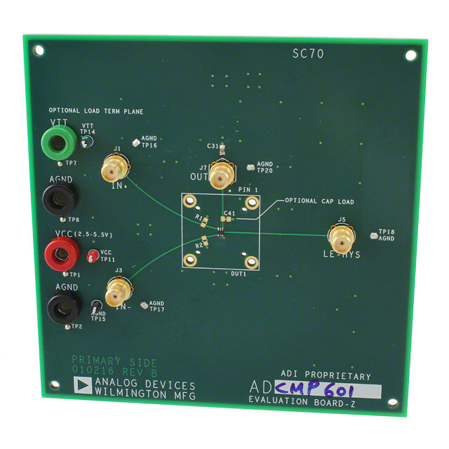
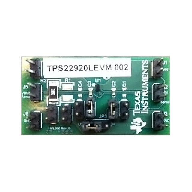
EVAL-ADCMP601BKSZ 是由 Analog Devices Inc. 提供的一款评估板,用于评估 ADCMP601 高速比较器的性能。该评估板属于“评估和演示板及套件”类别,主要应用于需要高速信号检测、电平转换和精密触发的场景。以下是其主要应用场景:

1. 通信系统:在高速通信系统中,ADCMP601 可用于信号接收端的阈值检测,快速判断输入信号是否超过设定的参考电压。EVAL-ADCMP601BKSZ 为设计人员提供了测试和优化比较器参数的平台,确保系统能够在高数据速率下稳定运行。

2. 工业自动化:该评估板可用于工业控制中的传感器信号处理。例如,在光电传感器或压力传感器的应用中,通过设置适当的阈值,比较器可以快速响应输入信号的变化,从而实现精准的控制功能。

3. 消费电子设备:在音频设备、视频切换器或其他需要快速信号切换的消费电子产品中,此评估板可帮助开发人员验证 ADCMP601 的性能,确保其能够满足产品对低延迟和高精度的要求。

4. 医疗设备:对于心电图(ECG)监测仪或超声波设备等医疗应用,EVAL-ADCMP601BKSZ 能够协助工程师评估比较器在信号调理阶段的表现,确保关键信号的准确捕捉和处理。

5. 汽车电子:在汽车行业中,该评估板可用于测试 ADCMP601 在碰撞检测、发动机控制单元(ECU)或车载网络中的表现,支持快速响应和高可靠性需求。

总之,EVAL-ADCMP601BKSZ 为设计人员提供了一个灵活的工具,用于探索 ADCMP601 的特性和潜力,适用于各种需要高速、低功耗和高精度比较器的场景。
| 参数 | 数值 |
| 产品目录 | 编程器,开发系统嵌入式解决方案 |
| 描述 | BOARD EVAL FOR ADCMP601 SC70-5放大器 IC 开发工具 EVAL-ADCMP601 |
| 产品分类 | |
| 品牌 | Analog Devices |
| 产品手册 | |
| 产品图片 |
|
| rohs | 符合RoHS无铅 / 符合限制有害物质指令(RoHS)规范要求 |
| 产品系列 | 模拟与数字IC开发工具,放大器 IC 开发工具,Analog Devices EVAL-ADCMP601BKSZ- |
| 数据手册 | |
| 产品型号 | EVAL-ADCMP601BKSZ |
| 主要属性 | CMOS 和 TTL 兼容输出 |
| 主要用途 | 比较器,单路 |
| 产品 | Evaluation Boards |
| 产品种类 | 放大器 IC 开发工具 |
| 使用的IC/零件 | ADCMP601 |
| 其它名称 | EVALADCMP601BKSZ |
| 商标 | Analog Devices |
| 封装 | Bulk |
| 嵌入式 | 否 |
| 工作电源电压 | 2.5 V to 5.5 V |
| 工具用于评估 | ADCMP601 |
| 工厂包装数量 | 1 |
| 所含物品 | 板 |
| 最大工作温度 | + 85 C |
| 最小工作温度 | - 40 C |
| 标准包装 | 1 |
| 类型 | Comparators |
| 系列 | ADCMP601 |
| 辅助属性 | 锁销启用引脚 |


- 商务部:美国ITC正式对集成电路等产品启动337调查
- 曝三星4nm工艺存在良率问题 高通将骁龙8 Gen1或转产台积电
- 太阳诱电将投资9.5亿元在常州建新厂生产MLCC 预计2023年完工
- 英特尔发布欧洲新工厂建设计划 深化IDM 2.0 战略
- 台积电先进制程称霸业界 有大客户加持明年业绩稳了
- 达到5530亿美元!SIA预计今年全球半导体销售额将创下新高
- 英特尔拟将自动驾驶子公司Mobileye上市 估值或超500亿美元
- 三星加码芯片和SET,合并消费电子和移动部门,撤换高东真等 CEO
- 三星电子宣布重大人事变动 还合并消费电子和移动部门
- 海关总署:前11个月进口集成电路产品价值2.52万亿元 增长14.8%

PDF Datasheet 数据手册内容提取
Rail-to-Rail, Very Fast, 2.5 V to 5.5 V, Single-Supply TTL/CMOS Comparators ADCMP600/ADCMP601/ADCMP602 FEATURES FUNCTIONAL BLOCK DIAGRAM Fully specified rail to rail at V = 2.5 V to 5.5 V CC Input common-mode voltage from −0.2 V to V + 0.2 V CC NONINVERTING Low glitch CMOS-/TTL-compatible output stage INPUT ADCMP600/ 3.5 ns propagation delay ADCMP601/ Q OUTPUT ADCMP602 10 mW at 3.3 V INVERTING INPUT Shutdown pin Single-pin control for programmable hysteresis and latch PImowpreorv seudp rpelpy lraecjeemcteionnt f>o 5r 0M dABX 999 (EXCEPT ADCLMEP/6H0Y0S) S(ADDNCMP602 ONLY) 05914-001 −40°C to +125°C operation Figure 1. APPLICATIONS High speed instrumentation Clock and data signal restoration Logic level shifting or translation Pulse spectroscopy High speed line receivers Threshold detection Peak and zero-crossing detectors High speed trigger circuitry Pulse-width modulators Current/voltage-controlled oscillators Automatic test equipment (ATE) GENERAL DESCRIPTION The ADCMP600, ADCMP601, and ADCMP602 are very fast input signal range while still allowing independent output comparators fabricated on XFCB2, an Analog Devices, Inc. swing control and power savings. proprietary process. These comparators are exceptionally The TTL-/CMOS-compatible output stage is designed to drive versatile and easy to use. Features include an input range from up to 5 pF with full timing specs and to degrade in a graceful GND − 0.5 V to VCC + 0.2 V, low noise, TTL-/CMOS-compatible and linear fashion as additional capacitance is added. The output drivers, and latch inputs with adjustable hysteresis comparator input stage offers robust protection against large and/or shutdown inputs. input overdrive, and the outputs do not phase reverse when the The device offers 5 ns propagation delay with 10 mV overdrive valid input signal range is exceeded. Latch and programmable on 3 mA typical supply current. hysteresis features are also provided with a unique single-pin control option. A flexible power supply scheme allows the devices to operate with a single +2.5 V positive supply and a −0.5 V to +2.8 V The ADCMP600 is available in 5-lead SC70 and SOT-23 input signal range up to a +5.5 V positive supply with a −0.5 V packages, the ADCMP601 is available in a 6-lead SC70 package, to +5.8 V input signal range. Split input/output supplies with no and the ADCMP602 is available in an 8-lead MSOP package. sequencing restrictions on the ADCMP602 support a wide Rev. A Information furnished by Analog Devices is believed to be accurate and reliable. However, no responsibility is assumed by Analog Devices for its use, nor for any infringements of patents or other One Technology Way, P.O. Box 9106, Norwood, MA 02062-9106, U.S.A. rights of third parties that may result from its use. Specifications subject to change without notice. No license is granted by implication or otherwise under any patent or patent rights of Analog Devices. Tel: 781.329.4700 www.analog.com Trademarks and registered trademarks are the property of their respective owners. Fax: 781.461.3113 ©2006–2011 Analog Devices, Inc. All rights reserved.
ADCMP600/ADCMP601/ADCMP602 TABLE OF CONTENTS Features .............................................................................................. 1 Application Information ................................................................ 10 Applications ....................................................................................... 1 Power/Ground Layout and Bypassing ..................................... 10 Functional Block Diagram .............................................................. 1 TTL-/CMOS-Compatible Output Stage ................................. 10 General Description ......................................................................... 1 Using/Disabling the Latch Feature ........................................... 10 Revision History ............................................................................... 2 Optimizing Performance ........................................................... 11 Specifications ..................................................................................... 3 Comparator Propagation Delay Dispersion ........................... 11 Electrical Characteristics ............................................................. 3 Comparator Hysteresis .............................................................. 11 Timing Information ......................................................................... 5 Crossover Bias Point .................................................................. 12 Absolute Maximum Ratings ............................................................ 6 Minimum Input Slew Rate Requirement ................................ 12 Thermal Resistance ...................................................................... 6 Typical Application Circuits ......................................................... 13 ESD Caution .................................................................................. 6 Outline Dimensions ....................................................................... 14 Pin Configuration and Function Descriptions ............................. 7 Ordering Guide .......................................................................... 16 Typical Performance Characteristics ............................................. 8 REVISION HISTORY 1/11—Rev. 0 to Rev. A Changed V Pin to GND ............................................. Throughout EE Changes to Common-Mode Dispersion Conditions................... 4 Changes to Figure 15 and Figure 16 ............................................... 9 Changes to Comparator Hysteresis Section ................................ 12 Updated Outline Dimensions ....................................................... 14 Changes to Ordering Guide .......................................................... 15 10/06—Revision 0: Initial Version Rev. A | Page 2 of 16
ADCMP600/ADCMP601/ADCMP602 SPECIFICATIONS ELECTRICAL CHARACTERISTICS V = V = 2.5 V, T = 25°C, unless otherwise noted. CCI CCO A Table 1. Parameter Symbol Conditions Min Typ Max Unit DC INPUT CHARACTERISTICS Voltage Range V, V V = 2.5 V to 5.5 V −0.5 V + 0.2 V P N CC CC Common-Mode Range V = 2.5 V to 5.5 V −0.2 V + 0.2 V CC CC Differential Voltage V = 2.5 V to 5.5 V V + 0.8 V CC CC Offset Voltage V −5.0 ±2 +5.0 mV OS Bias Current I, I −5.0 ±2 +5.0 µA P N Offset Current −2.0 +2.0 µA Capacitance C, C 1 pF P N Resistance, Differential Mode −0.1 V to V 200 700 kΩ CC Resistance, Common Mode −0.5 V to V + 0.5 V 100 350 kΩ CC Active Gain A 85 dB V Common-Mode Rejection Ratio CMRR V = 2.5 V, V = 2.5 V, 50 dB CCI CCO V = −0.2 V to +2.7 V CM V = 2.5 V, V = 5.5 V 50 dB CCI CCO Hysteresis (ADCMP600) 2 mV Hysteresis (ADCMP601/ADCMP602) R = ∞ 0.1 mV HYS LATCH ENABLE PIN CHARACTERISTICS (ADCMP601/ADCMP602 Only) V Hysteresis is shut off 2.0 V V IH CC V Latch mode guaranteed −0.2 +0.4 +0.8 V IL I V = V −6 +6 µA IH IH CC I V = 0.4 V −0.1 +0.1 mA OL IL HYSTERESIS MODE AND TIMING (ADCMP601/ADCMP602 Only) Hysteresis Mode Bias Voltage Current −1 μA 1.145 1.25 1.35 V Resistor Value Hysteresis = 120 mV 65 80 120 kΩ Hysteresis Current Hysteresis = 120 mV −18 −12 −7 µA Latch Setup Time t V = 50 mV −2 ns S OD Latch Hold Time t V = 50 mV 2.6 ns H OD Latch-to-Output Delay t , t V = 50 mV 27 ns PLOH PLOL OD Latch Minimum Pulse Width t V = 50 mV 21 ns PL OD SHUTDOWN PIN CHARACTERISTICS (ADCMP602 Only) V Comparator is operating 2.0 V V IH CCO V Shutdown guaranteed −0.2 +0.4 +0.6 V IL I V = V −6 6 µA IH IH CC I V = 0 V −100 µA OL IL Sleep Time t I < 500 µA 20 ns SD CCO Wake-Up Time t V = 100 mV, output valid 50 ns H OD DC OUTPUT CHARACTERISTICS V = 2.5 V to 5.5 V CCO Output Voltage High Level V I = 8 mA, V = 2.5 V V − 0.4 V OH OH CCO CC Output Voltage Low Level V I = 8 mA, V = 2.5 V 0.4 V OL OL CCO Output Voltage High Level at −40°C V I = 6 mA, V = 2.5 V V − 0.4 V OH OH CCO CC Output Voltage Low Level at− 40°C V I = 6 mA, V = 2.5 V 0.4 V OL OL CCO Rev. A | Page 3 of 16
ADCMP600/ADCMP601/ADCMP602 Parameter Symbol Conditions Min Typ Max Unit AC PERFORMANCE1 Rise Time /Fall Time t t 10% to 90%, V = 2.5 V 2.2 ns R F CCO 10% to 90%, V = 5.5 V 4 ns CCO Propagation Delay t V = 50 mV, V = 2.5 V 3.5 ns PD OD CCO V = 50 mV, V = 5.5 V 4.3 ns OD CCO V = 10 mV, V = 2.5 V 5 ns OD CCO Propagation Delay Skew—Rising to V = 2.5 V to 5.5 V 500 ps CCO Falling Transition V = 50 mV OD Overdrive Dispersion 10 mV < V < 125 mV 1.2 ns OD Common-Mode Dispersion −0.2 V < V < V + 0.2 V 200 ps CM CCI V = 50 mV OD Minimum Pulse Width PW V = V = 2.5 V 3 ns MIN CCI CCO PW = 90% of PW OUT IN V = V = 5.5 V 4.5 ns CCI CCO PW = 90% of PW OUT IN POWER SUPPLY Input Supply Voltage Range V 2.5 5.5 V CCI Output Supply Voltage Range V 2.5 5.5 V CCO Positive Supply Differential V − V Operating −3.0 +3.0 V CCI CCO (ADCMP602 Only) V − V Nonoperating −5.5 +5.5 V CCI CCO Positive Supply Current I V = 2.5 V 3 3.5 mA VCC CC (ADCMP600/ADCMP601) V = 5.5 V 3.5 4.0 CC Input Section Supply Current I V = 2.5 V 0.9 1.4 mA VCCI CCI (ADCMP602 Only) V = 5.5 V 1.2 2.0 mA CCI Output Section Supply Current I V = 2.5 V 1.45 3.0 mA VCCO CCO (ADCMP602 Only) V = 5.5 V 2.1 3.5 mA CCO Power Dissipation P V = 2.5 V 7 9 mW D CC P V = 5.5 V 20 23 mW D CC Power Supply Rejection Ratio PSRR V = 2.5 V to 5 V −50 dB CCI Shutdown Mode I V = 2.5 V 240 400 µA CCI CC (ADCMP602 Only) Shutdown Mode I V =2.5 V 30 µA CCO CC (ADCMP602 Only) 1 V = 100 mV square input at 50 MHz, V = 0 V, CL = 5 pF, V = V =2.5 V, unless otherwise noted. IN CM CCI CCO Rev. A | Page 4 of 16
ADCMP600/ADCMP601/ADCMP602 TIMING INFORMATION Figure 2 illustrates the ADCMP600/ADCMP601/ADCMP602 latch timing relationships. Table 2 provides definitions of the terms shown in Figure 2. 1.1V LATCH ENABLE tS tPL tH DIFFERENTIAL VIN INPUT VOLTAGE VN ± VOS VOD tPDL tPLOH Q OUTPUT 50% tF 05914-025 Figure 2. System Timing Diagram Table 2. Timing Descriptions Symbol Timing Description t Input to output high delay Propagation delay measured from the time the input signal crosses the reference (± the PDH input offset voltage) to the 50% point of an output low-to-high transition. t Input to output low delay Propagation delay measured from the time the input signal crosses the reference (± the PDL input offset voltage) to the 50% point of an output high-to-low transition. t Latch enable to output high delay Propagation delay measured from the 50% point of the latch enable signal low-to-high PLOH transition to the 50% point of an output low-to-high transition. t Latch enable to output low delay Propagation delay measured from the 50% point of the latch enable signal low-to-high PLOL transition to the 50% point of an output high-to-low transition. t Minimum hold time Minimum time after the negative transition of the latch enable signal that the input signal H must remain unchanged to be acquired and held at the outputs. t Minimum latch enable pulse width Minimum time that the latch enable signal must be high to acquire an input signal change. PL t Minimum setup time Minimum time before the negative transition of the latch enable signal occurs that an S input signal change must be present to be acquired and held at the outputs. t Output rise time Amount of time required to transition from a low to a high output as measured at the 20% R and 80% points. t Output fall time Amount of time required to transition from a high to a low output as measured at the 20% F and 80% points. V Voltage overdrive Difference between the input voltages V and V. OD A B Rev. A | Page 5 of 16
ADCMP600/ADCMP601/ADCMP602 ABSOLUTE MAXIMUM RATINGS Stresses above those listed under Absolute Maximum Ratings Table 3. may cause permanent damage to the device. This is a stress Parameter Rating rating only; functional operation of the device at these or any Supply Voltages other conditions above those indicated in the operational Input Supply Voltage (V to GND) −0.5 V to +6.0 V CCI section of this specification is not implied. Exposure to absolute Output Supply Voltage −0.5 V to +6.0 V maximum rating conditions for extended periods may affect (V to GND) CCO device reliability. Positive Supply Differential −6.0 V to +6.0 V (VCCI − VCCO) THERMAL RESISTANCE Input Voltages θ is specified for the worst-case conditions, that is, a device Input Voltage −0.5 V to V + 0.5 V JA CCI soldered in a circuit board for surface-mount packages. Differential Input Voltage ±(V + 0.5 V) CCI Maximum Input/Output Current ±50 mA Table 4. Thermal Resistance Shutdown Control Pin Package Type θ 1 Unit JA Applied Voltage (HYS to GND) −0.5 V to V + 0.5 V ADCMP600 SC70 5-Lead 426 °C/W CCO Maximum Input/Output Current ±50 mA ADCMP600 SOT-23 5-Lead 302 °C/W Latch/Hysteresis Control Pin ADCMP601 SC70 6-Lead 426 °C/W Applied Voltage (HYS to GND) −0.5 V to V + 0.5 V ADCMP602 MSOP 5-Lead 130 °C/W CCO 1 Measurement in still air. Maximum Input/Output Current ±50 mA ESD CAUTION Output Current ±50 mA Temperature Operating Temperature, Ambient −40°C to +125°C Operating Temperature, Junction 150°C Storage Temperature Range −65°C to +150°C Rev. A | Page 6 of 16
ADCMP600/ADCMP601/ADCMP602 PIN CONFIGURATION AND FUNCTION DESCRIPTIONS Q 1 ADCMP600 5 VCCI/VCCO Q 1 ADCMP601 6 VCCI/VCCO VCCI 1 8 VCCO ADCMP602 GND 2 TOP VIEW GND 2 TOP VIEW 5 LE/HYS VP 2 7 Q (Not to Scale) (Not to Scale) TOP VIEW VP 3 4 VN 05914-002 VP 3 4 VN 05914-003 SVDNN 43 (Not to Scale) 65 GLEN/DHYS 05914-004 Figure 3. ADCMP600 Pin Configuration Figure 4. ADCMP601 Pin Configuration Figure 5. ADCMP602 Pin Configuration Table 5. ADCMP600 (SOT-23-5 and SC70-5) Pin Function Descriptions Pin No. Mnemonic Description 1 Q Noninverting Output. Q is at logic high if the analog voltage at the noninverting input, V, is greater P than the analog voltage at the inverting input, V . N 2 GND Negative Supply Voltage. 3 V Noninverting Analog Input. P 4 V Inverting Analog Input. N 5 V /V Input Section Supply/Output Section Supply. Shared pin. CCI CCO Table 6. ADCMP601 (SC70-6) Pin Function Descriptions Pin No. Mnemonic Description 1 Q Noninverting Output. Q is at logic high if the analog voltage at the noninverting input, V, is greater P than the analog voltage at the inverting input, V , if the comparator is in compare mode. N 2 GND Negative Supply Voltage. 3 V Noninverting Analog Input. P 4 V Inverting Analog Input. N 5 LE/HYS Latch/Hysteresis Control. Bias with resistor or current for hysteresis adjustment; drive low to latch. 6 V /V Input Section Supply/Output Section Supply. Shared pin. CCI CCO Table 7. ADCMP602 (MSOP-8) Pin Function Descriptions Pin No. Mnemonic Description 1 V Input Section Supply. CCI 2 V Noninverting Analog Input. P 3 V Inverting Analog Input. N 4 S Shutdown. Drive this pin low to shut down the device. DN 5 LE/HYS Latch/Hysteresis Control. Bias with resistor or current for hysteresis adjustment; drive low to latch. 6 GND Negative Supply Voltage. 7 Q Noninverting Output. Q is at logic high if the analog voltage at the noninverting input, V, is greater P than the analog voltage at the inverting input, V , if the comparator is in compare mode. N 8 V Output Section Supply. CCO Rev. A | Page 7 of 16
ADCMP600/ADCMP601/ADCMP602 TYPICAL PERFORMANCE CHARACTERISTICS V = V = 2.5 V, T = 25°C, unless otherwise noted. CCI CCO A 800 20 IOL VS VOL 600 15 VCC= 2.5V VCC= 5.5V IOH VS VOH 400 10 A) m ENT (µA) 2000 RRENT ( 50 R U R C CU –200 AD –5 O L –400 –10 ––860000 05914-007 ––1250 09514-011 –1 0 1 2 3 4 5 6 7 –1.0 –0.6 –0.2 0.2 0.6 1.0 1.4 1.8 2.2 2.6 3.0 3.4 LE/HYS (V) VOUT (V) Figure 6. LE/HYS Pin I/V Characteristics Figure 9. V /V vs. Current Load OH OL 150 250 100 VCC = 2.5V VCC = 5.5V 200 A) 50 mV) VCC= 5.5V RENT (µ 0 RESIS ( 150 R E CU YST 100 –50 H 50 –100 –150 05914-027 0 VCC= 2.5V 05914-008 –1 0 1 2 3 4 5 6 7 50 150 250 350 450 550 650 SHUTDOWN PIN VOLTAGE (V) HYSTERESIS RESISTOR (kΩ) Figure 7. S Pin I/V Characteristics Figure 10. Hysteresis vs. R Control Resistor DN HYS 20 450 VCC = 2.5V 400 15 350 10 V) 300 LOT 1 m A) 5 SIS ( 250 (µB 0 ERE 200 LOT 2 I T S –5 Y H 150 IB @ +125°C –10 100 IB @ +25°C ––2105 IB @ –40°C 05914-005 500 05914-026 –1.0 –0.5 0 0.5 1.0 1.5 2.0 2.5 3.0 3.5 0 –5 –10 –15 –20 COMMON-MODE VOLTAGE (V) PIN CURRENT (µA) Figure 8. Input Bias Current vs. Input Common Mode Figure 11. Hysteresis vs. Pin Current Rev. A | Page 8 of 16
ADCMP600/ADCMP601/ADCMP602 4.8 4.6 s) 4.4 n AY ( 4.2 L E N D 4.0 O ATI 3.8 G A P 3.6 O R P 3.4 33..02 05914-009 05914-012 0 10 20 30 40 50 60 70 80 90 100110120130140 1.00V/DIV M4.00ns OVERDRIVE (mV) Figure 12. Propagation Delay vs. Input Overdrive at V = 2.5 V Figure 15. 50 MHz Output Waveform V = 5.5 V CC CC 4.0 VCM AT VCC = 2.5V 3.8 s) n Y ( A L E 3.6 D N RISE O TI A G 3.4 A P O FALL R P 3.2 3.0–0.6 0 CO0M.6MON-MO1D.2E VOLT1A.G8E (V) 2.4 3.0 05914-028 05914-013 500mV/DIV M4.00ns Figure 13. Propagation Delay vs. Input Common-Mode Voltage Figure16. 50 MHz Output Waveforms @ 2.5 V at V = 2.5 V CC 5.0 4.8 4.6 s) n Y ( 4.4 A L E 4.2 D N O 4.0 TI A RISE G 3.8 A P O 3.6 R FALL P 3.4 33..02 05914-029 2.5 3.0 3.5 4.0 4.5 5.0 5.5 6.0 VCCO (V) Figure 14. Propagation Delay vs. V CCO Rev. A | Page 9 of 16
ADCMP600/ADCMP601/ADCMP602 APPLICATION INFORMATION POWER/GROUND LAYOUT AND BYPASSING This delay is measured to the 50% point for the supply in use; therefore, the fastest times are observed with the V supply at The ADCMP600/ADCMP601/ADCMP602 comparators are very CC 2.5 V, and larger values are observed when driving loads that high speed devices. Despite the low noise output stage, it is essential switch at other levels. to use proper high speed design techniques to achieve the specified performance. Because comparators are uncompensated amplifiers, When duty cycle accuracy is critical, the logic being driven feedback in any phase relationship is likely to cause oscillations or should switch at 50% of V and load capacitance should be CC undesired hysteresis. Of critical importance is the use of low minimized. When in doubt, it is best to power V or the CCO impedance supply planes, particularly the output supply plane entire device from the logic supply and rely on the input PSRR (V ) and the ground plane (GND). Individual supply planes are and CMRR to reject noise. CCO recommended as part of a multilayer board. Providing the lowest Overdrive and input slew rate dispersions are not significantly inductance return path for switching currents ensures the best affected by output loading and V variations. CC possible performance in the target application. The TTL-/CMOS-compatible output stage is shown in the It is also important to adequately bypass the input and output simplified schematic diagram (Figure 17). Because of its supplies. Multiple high quality 0.01 µF bypass capacitors should inherent symmetry and generally good behavior, this output be placed as close as possible to each of the V and V supply CCI CCO stage is readily adaptable for driving various filters and other pins and should be connected to the GND plane with redundant unusual loads. vias. At least one of these should be placed to provide a physically short return path for output currents flowing back from ground VLOGIC to the V pin. High frequency bypass capacitors should be CC carefully selected for minimum inductance and ESR. Parasitic A1 Q1 layout inductance should also be strictly controlled to maximize the effectiveness of the bypass at high frequencies. If the package allows and the input and output supplies have +IN OUTPUT been connected separately such that V ≠ V , care should be AV CCI CCO –IN taken to bypass each of these supplies separately to the GND plane. A bypass capacitor should never be connected between them. It is recommended that the GND plane separate the V CCI A2 Q2 and V planes when the circuit board layout is designed to CCO madivnainmtaizgee coofu tphlei nagd dbiettiwoneaenl b tyhpea tsws oc aspuapcpitliaensc aen fdro tmo teaakceh GAIN STAGE OUTPUT STAGE 05914-014 Figure 17. Simplified Schematic Diagram of respective supply to the ground plane. This enhances the TTL-/CMOS-Compatible Output Stage performance when split input/output supplies are used. If the USING/DISABLING THE LATCH FEATURE input and output supplies are connected together for single-supply operation such that V = V , coupling between the two supplies The latch input is designed for maximum versatility. It can CCI CCO is unavoidable; however, careful board placement can help keep safely be left floating for fixed hysteresis or be tied to V to CC output return currents away from the inputs. remove the hysteresis, or it can be driven low by any standard TTL-/CMOS-COMPATIBLE OUTPUT STAGE TTL/CMOS device as a high speed latch. In addition, the pin can be operated as a hysteresis control pin Specified propagation delay performance can be achieved only with a bias voltage of 1.25 V nominal and an input resistance of by keeping the capacitive load at or below the specified minimums. approximately 7000 Ω. This allows the comparator hysteresis to The outputs of the devices are designed to directly drive one be easily and accurately controlled by either a resistor or an Schottky TTL or three low power Schottky TTL loads or the inexpensive CMOS DAC. equivalent. For large fan outputs, buses, or transmission lines, use an appropriate buffer to maintain the excellent speed and Hysteresis control and latch mode can be used together if an stability of the comparator. open drain, an open collector, or a three-state driver is connected parallel to the hysteresis control resistor or current source. With the rated 5 pF load capacitance applied, more than half of the total device propagation delay is output stage slew time, Due to the programmable hysteresis feature, the logic threshold even at 2.5 V V . Because of this, the total prop delay decreases of the latch pin is approximately 1.1 V regardless of V . CC CC as V decreases, and instability in the power supply may CCO appear as excess delay dispersion. Rev. A | Page 10 of 16
ADCMP600/ADCMP601/ADCMP602 OPTIMIZING PERFORMANCE INPUT VOLTAGE 1V/ns As with any high speed comparator, proper design and layout techniques are essential for obtaining the specified performance. VN ± VOS Stray capacitance, inductance, inductive power and ground 10V/ns impedances, or other layout issues can severely limit performance and often cause oscillation. Large discontinuities along input and output transmission lines can also limit the specified pulse- wbei dmthin dimispizeerdsi aosn m puercfho rams iasn pcrea.c Ttihcaeb sloe.u Hrcieg him sopuerdcaen icme psehdoaunldce , Q/Q OUTPUT DISPERSION 05914-016 in combination with the parasitic input capacitance of the Figure 19. Propagation Delay—Slew Rate Dispersion comparator, causes an undesirable degradation in bandwidth at COMPARATOR HYSTERESIS the input, thus degrading the overall response. Thermal noise from large resistances can easily cause extra jitter with slowly The addition of hysteresis to a comparator is often desirable in a slewing input signals; higher impedances encourage undesired noisy environment, or when the differential input amplitudes coupling. are relatively small or slow moving. Figure 20 shows the transfer function for a comparator with hysteresis. As the input voltage COMPARATOR PROPAGATION DELAY approaches the threshold (0.0 V, in this example) from below DISPERSION the threshold region in a positive direction, the comparator The ADCMP600/ADCMP601/ADCMP602 comparators are switches from low to high when the input crosses +V /2, and the H designed to reduce propagation delay dispersion over a wide new switching threshold becomes −V /2. The comparator remains H input overdrive range. Propagation delay dispersion is the in the high state until the new threshold, −V /2, is crossed from H variation in propagation delay that results from a change in the below the threshold region in a negative direction. In this manner, degree of overdrive or slew rate (that is, how far or how fast the noise or feedback output signals centered on 0.0 V input cannot input signal exceeds the switching threshold). cause the comparator to switch states unless it exceeds the region bounded by ±V /2. Propagation delay dispersion is a specification that becomes H important in high speed, time-critical applications, such as data OUTPUT communication, automatic test and measurement, and instru- mentation. It is also important in event-driven applications, such as pulse spectroscopy, nuclear instrumentation, and medical VOH imaging. Dispersion is defined as the variation in propagation delay as the input overdrive conditions are changed (Figure 18 and Figure 19). VOL The device dispersion is typically < 2 ns as the overdrive varies from 10 mV to 125 mV. This specification applies to both positive and negative signals because the device has very closely matched delays both positive-going an50d0 mnVe gOaVtEiRvDeR-gIVoEing inputs. –V2H 0 +V2H INPUT 05914-017 Figure 20. Comparator Hysteresis Transfer Function The customary technique for introducing hysteresis into a INPUT VOLTAGE comparator uses positive feedback from the output back to the 10mV OVERDRIVE input. One limitation of this approach is that the amount of VN ± VOS hysteresis varies with the output logic levels, resulting in hysteresis that is not symmetric about the threshold. The external feedback network can also introduce significant Q/Q OUTPUT DISPERSION 05914-015 posacrialslaittiicosn t hina ts roemdue ccea sheisg.h speed performance and induce Figure 18. Propagation Delay—Overdrive Dispersion These ADCMP600 features a fixed hysteresis of approximately 2 mV. The ADCMP601 and ADCMP602 comparators offer a programmable Hysteresis feature that can significantly improve accuracy and stability. Connecting an external pull-down resistor or a current source from the LE/HYS pin to GND, varies the amount of hysteresis in a predictable, stable manner. Rev. A | Page 11 of 16
ADCMP600/ADCMP601/ADCMP602 Leaving the LE/HYS pin disconnected results in a fixed 250 hysteresis of 2 mV; driving this pin high removes hysteresis. The maximum hysteresis that can be applied using this pin is 200 approximately 160 mV. Figure 21 illustrates the amount of hysteresis applied as a function of the external resistor value, mV) VCC= 5.5V and Figure 11 illustrates hysteresis as a function of the current. S ( 150 SI E R The hysteresis control pin appears as a 1.25 V bias voltage seen E ST 100 through a series resistance of 7 kΩ. The bias voltage changes Y H ± 20% throughout the hysteresis control range. The advantages of applying hysteresis in this manner are improved accuracy, 50 ivmerpsraotivlietdy. sAtanb ielxittye, rrneadlu bcyepda csos mcappoancietnotr ciso unnott, raencdo mmmaxeinmduemd o n 0 VCC= 2.5V 05914-030 the HYS pin because it impairs the latch function and often 50 150 250 350 450 550 650 HYSTERESIS RESISTOR (kΩ) degrades the jitter performance of the device. As described in the Figure 21. Hysteresis vs. R Control Resistor HYS Using/Disabling the Latch Feature section, hysteresis control MINIMUM INPUT SLEW RATE REQUIREMENT need not compromise the latch function. CROSSOVER BIAS POINT With the rated load capacitance and normal good PC Board design practice, as discussed in the Optimizing Performance In both op amps and comparators, rail-to-rail inputs of this type section, these comparators should be stable at any input slew have a dual front-end design. Certain devices are active near the rate with no hysteresis. Broadband noise from the input stage is V rail and others are active near the GND rail. At some predeter- CC observed in place of the violent chattering seen with most other mined point in the common-mode range, a crossover occurs. At high speed comparators. With additional capacitive loading or this point, normally V /2, the direction of the bias current reverses CC poor bypassing, oscillation is observed. This oscillation is due to and the measured offset voltages and currents change. the high gain bandwidth of the comparator in combination with The ADCMP600/ADCMP601/ADCMP602 comparators feedback parasitics in the package and PC board. In many slightly elaborate on this scheme. Crossover points can be found applications, chattering is not harmful. at approximately 0.8 V and 1.6 V. Rev. A | Page 12 of 16
ADCMP600/ADCMP601/ADCMP602 TYPICAL APPLICATION CIRCUITS 5V 0.1µF 2.5V 2kΩ 2kΩ ADCMP600 OUTPUT 0.1µF 05914-019 CMOS Figure 22. Self-Biased, 50% Slicer ADCMP600 PWM OUTPUT INPUT 1.25V ±50mV INPUT 1.25V 10kΩ REF CMOS VDD 10kΩ 2.5V TO 5V ADCMP601 100Ω ADCMP600 CMOS 10kΩ 82pF LE/HYS 05914-020 40kΩ 05914-022 Figure 23. LVDS-to-CMOS Receiver Figure 25. Oscillator and Pulse-Width Modulator 2.5V TO 5V 2.5V 10kΩ ADCMP601 20kΩ ADCMP601 OUTPUT 1.5MHz TO 30MHz DIGITAL 74 AHC LE/HYS 20kΩ 82pF LE/HYS INPUT 1G07 0CVVOO TNLOTT AR2.GO5VEL 100kΩ 100kΩ 05914-021 HYSCTUERRREESNITS 10kΩ 05914-023 Figure 24. Voltage-Controlled Oscillator Figure 26. Hysteresis Adjustment with Latch Rev. A | Page 13 of 16
ADCMP600/ADCMP601/ADCMP602 OUTLINE DIMENSIONS 2.20 2.00 1.80 1.35 5 4 2.40 1.25 2.10 1.15 1 2 3 1.80 0.65BSC 1.00 1.10 0.40 0.90 0.80 0.10 0.70 0.46 0.10MAX 0.30 SPELAATNIENG 00..2028 0.36 COPLANARITY 0.15 0.26 0.10 COMPLIANTTOJEDECSTANDARDSMO-203-AA 072809-A Figure 27. 5-Lead Thin Shrink Small Outline Transistor Package (SC70) (KS-5) Dimensions shown in millimeters 3.00 2.90 2.80 1.70 5 4 3.00 1.60 2.80 1.50 2.60 1 2 3 0.95BSC 1.90 BSC 1.30 1.15 0.90 1.45MAX 0.20MAX 0.95MIN 0.08MIN 0.55 0.15MAX 10° 0.45 0.05MIN 0.50MAX SPELAATNIENG 5° B0S.6C0 0.35 0.35MIN 0° COMPLIANTTOJEDECSTANDARDSMO-178-AA 11-01-2010-A Figure 28. 5-Lead Small Outline Transistor Package (SOT-23) (RJ-5) Dimensions shown in millimeters Rev. A | Page 14 of 16
ADCMP600/ADCMP601/ADCMP602 2.20 2.00 1.80 1.35 6 5 4 2.40 1.25 2.10 1.15 1 2 3 1.80 0.65BSC 1.30BSC 1.00 1.10 0.40 0.90 0.80 0.10 0.70 0.46 0.10MAX 0.30 SPELAATNIENG 00..2028 0.36 COPLANARITY 0.15 0.26 0.10 COMPLIANTTOJEDECSTANDARDSMO-203-AB 072809-A Figure 29. 6-Lead Thin Shrink Small Outline Transistor Package (SC70) (KS-6) Dimensions shown in millimeters 3.20 3.00 2.80 8 5 5.15 3.20 4.90 3.00 4.65 2.80 1 4 PIN1 IDENTIFIER 0.65BSC 0.95 15°MAX 0.85 1.10MAX 0.75 0.80 0.15 0.40 6° 0.23 0.55 CO0P.0L50A.1N0ARICTOYMPLIANT0.T25OJEDECSTA0°NDARDS0M.0O9-187-AA 0.40 10-07-2009-B Figure 30. 8-Lead Mini Small Outline Package (MSOP) (RM-8) Dimensions shown in millimeters Rev. A | Page 15 of 16
ADCMP600/ADCMP601/ADCMP602 ORDERING GUIDE Model1 Temperature Range Package Description Package Option Branding ADCMP600BRJZ-R2 −40°C to +125°C 5-Lead SOT23 RJ-5 G0C ADCMP600BRJZ-RL −40°C to +125°C 5-Lead SOT23 RJ-5 G0C ADCMP600BRJZ-REEL7 −40°C to +125°C 5-Lead SOT23 RJ-5 G0C ADCMP600BKSZ-R2 −40°C to +125°C 5-Lead SC70 KS-5 G0C ADCMP600BKSZ-RL −40°C to +125°C 5-Lead SC70 KS-5 G0C ADCMP600BKSZ-REEL7 −40°C to +125°C 5-Lead SC70 KS-5 G0C ADCMP601BKSZ-R2 −40°C to +125°C 6-Lead SC70 KS-6 G0N ADCMP601BKSZ-RL −40°C to +125°C 6-Lead SC70 KS-6 G0N ADCMP601BKSZ-REEL7 −40°C to +125°C 6-Lead SC70 KS-6 G0N ADCMP602BRMZ −40°C to +125°C 8-Lead MSOP RM-8 GF ADCMP602BRMZ-REEL −40°C to +125°C 8-Lead MSOP RM-8 GF ADCMP602BRMZ-REEL7 −40°C to +125°C 8-Lead MSOP RM-8 GF EVAL-ADCMP600BRJZ Evaluation Board EVAL-ADCMP600BKSZ Evaluation Board EVAL-ADCMP601BKSZ Evaluation Board EVAL-ADCMP602BRMZ Evaluation Board 1 Z = RoHS Compliant Part. ©2006–2011 Analog Devices, Inc. All rights reserved. Trademarks and registered trademarks are the property of their respective owners. D05914-0-1/11(A) Rev. A | Page 16 of 16
Mouser Electronics Authorized Distributor Click to View Pricing, Inventory, Delivery & Lifecycle Information: A nalog Devices Inc.: ADCMP600BKSZ-R2 ADCMP600BRJZ-R2 ADCMP600BRJZ-REEL7 ADCMP601BKSZ-R2 ADCMP601BKSZ- REEL7 ADCMP602BRMZ ADCMP600BKSZ-REEL7 ADCMP600BRJZ-RL ADCMP602BRMZ-REEL ADCMP602BRMZ-REEL7 EVAL-ADCMP600BKSZ EVAL-ADCMP600BRJZ EVAL-ADCMP602BRMZ EVAL- ADCMP601BKSZ