
 Datasheet下载
- 型号: ESDAXLC6-1MY2
- 制造商: STMicroelectronics
- 库位|库存: xxxx|xxxx
- 要求:
| 数量阶梯 | 香港交货 | 国内含税 |
| +xxxx | $xxxx | ¥xxxx |
查看当月历史价格
查看今年历史价格
ESDAXLC6-1MY2产品简介:
ICGOO电子元器件商城为您提供ESDAXLC6-1MY2由STMicroelectronics设计生产,在icgoo商城现货销售,并且可以通过原厂、代理商等渠道进行代购。 ESDAXLC6-1MY2价格参考。STMicroelectronicsESDAXLC6-1MY2封装/规格:TVS - 二极管, 。您可以下载ESDAXLC6-1MY2参考资料、Datasheet数据手册功能说明书,资料中有ESDAXLC6-1MY2 详细功能的应用电路图电压和使用方法及教程。
STMicroelectronics(意法半导体)生产的ESDAXLC6-1MY2是一款瞬态电压抑制二极管(TVS Diode),属于ESDAXLC系列,主要用于保护电子设备免受静电放电(ESD)、电涌和其他瞬态过电压事件的损害。以下是该型号的主要应用场景:

 1. 消费电子产品
   - 智能手机和平板电脑:保护数据接口(如USB、HDMI、MIPI等)和显示屏信号线,防止因静电或外部干扰导致的损坏。
   - 音频设备:用于耳机插孔、麦克风输入和其他音频接口的保护,确保音质稳定。
   - 家用电器:如电视、音响系统、游戏机等,保护其控制电路和通信接口。

 2. 通信设备
   - 网络设备:例如路由器、交换机、调制解调器等,用于保护以太网端口、Wi-Fi模块和天线接口。
   - 工业通信模块:保护RS-232、RS-485等串行通信接口,防止过电压对数据传输的影响。

 3. 汽车电子
   - 车载信息娱乐系统:保护触摸屏、导航模块和音频输出接口。
   - 传感器接口:如倒车雷达、摄像头等,防止外部环境中的静电或电涌干扰。
   - 车载网络:保护CAN总线、LIN总线等通信线路。

 4. 工业自动化
   - 人机界面(HMI):保护触摸屏和按钮输入接口。
   - 传感器与执行器:用于保护模拟信号输入、数字信号输入和输出接口。
   - PLC模块:保护通信端口和电源输入端,避免因电涌导致系统故障。

 5. 医疗设备
   - 便携式医疗设备:如血压计、血糖仪等,保护其数据接口和电池充电接口。
   - 大型医疗设备:如超声波设备、心电图机等,保护其敏感的信号处理电路。

 6. 物联网(IoT)设备
   - 智能家居设备:如智能灯泡、智能插座等,保护无线通信模块(Wi-Fi、蓝牙、Zigbee)。
   - 可穿戴设备:如智能手表、健康手环,保护其小型化接口和传感器。

 特性总结
ESDAXLC6-1MY2具有低电容特性(典型值为0.3pF),非常适合高速数据线路的保护,同时具备高响应速度和良好的箝位性能,能够有效抑制瞬态电压,确保电子设备的可靠性和稳定性。
| 参数 | 数值 |
| 产品目录 | |
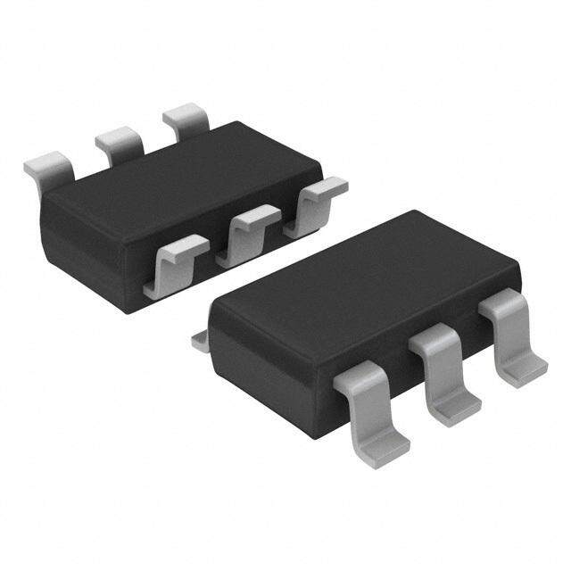
| 描述 | TVS DIODE 3VWM SOD882TVS 二极管 - 瞬态电压抑制器 0.35 pF max 200 - 300 MHz .55 mm 3B |
| 产品分类 | |
| 品牌 | STMicroelectronics |
| 产品手册 | |
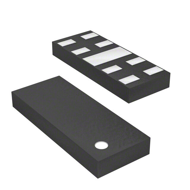
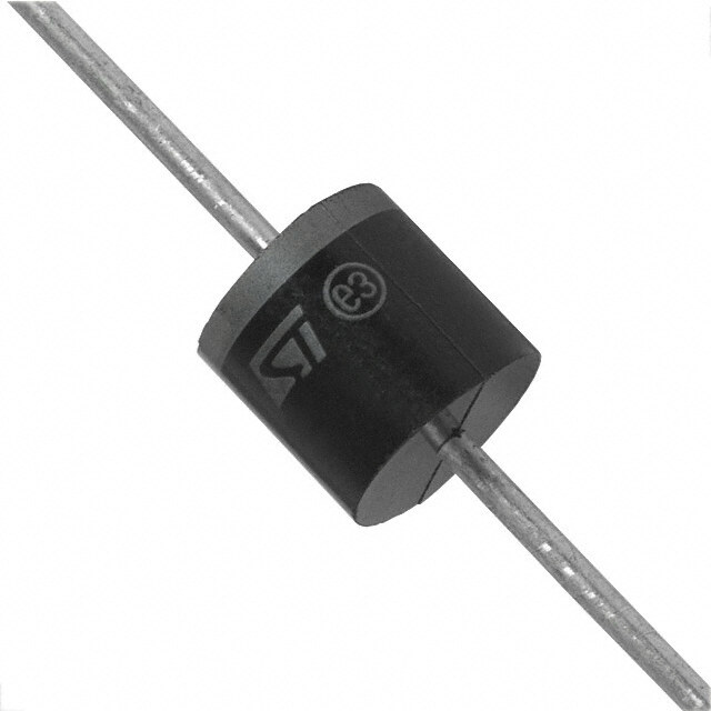
| 产品图片 |
|
| rohs | 符合RoHS无铅 / 符合限制有害物质指令(RoHS)规范要求 |
| 产品系列 | 二极管与整流器,TVS二极管,TVS 二极管 - 瞬态电压抑制器,STMicroelectronics ESDAXLC6-1MY2ESDA, TRANSIL™ |
| 数据手册 | |
| 产品型号 | ESDAXLC6-1MY2 |
| 不同频率时的电容 | 0.35pF @ 200MHz ~ 3GHz |
| 产品种类 | TVS 二极管 - 瞬态电压抑制器 |
| 供应商器件封装 | SOD-882 |
| 其它名称 | 497-10561-6 |
| 其它有关文件 | http://www.st.com/web/catalog/sense_power/FM114/CL1137/SC1768/PF250136?referrer=70071840http://www.st.com/web/catalog/sense_power/FM114/CL1137/SC492/SS1421/PF250136?referrer=70071840 |
| 击穿电压 | 6 V |
| 功率-峰值脉冲 | 12W |
| 包装 | Digi-Reel® |
| 单向通道 | 1 |
| 双向通道 | - |
| 商标 | STMicroelectronics |
| 安装类型 | 表面贴装 |
| 安装风格 | SMD/SMT |
| 封装 | Reel |
| 封装/外壳 | SOD-882 |
| 封装/箱体 | UQFN-2L |
| 尺寸 | 0.6 mm W x 1 mm L x 0.5 mm H |
| 峰值脉冲功率耗散 | 12 W |
| 工作温度 | -30°C ~ 85°C |
| 工厂包装数量 | 12000 |
| 应用 | 通用 |
| 最大工作温度 | + 85 C |
| 最小工作温度 | - 30 C |
| 极性 | Unidirectional |
| 标准包装 | 1 |
| 电压-击穿(最小值) | 6V |
| 电压-反向关态(典型值) | 3V |
| 电压-箝位(最大值)@Ipp | - |
| 电容 | 0.35 pF |
| 电流-峰值脉冲(10/1000µs) | 2.8A (8/20µs) |
| 电源线路保护 | 无 |
| 端接类型 | SMD/SMT |
| 类型 | 齐纳 |
| 系列 | ESDAXLC6-1MY2 |
| 钳位电压 | 6 V |


- 商务部:美国ITC正式对集成电路等产品启动337调查
- 曝三星4nm工艺存在良率问题 高通将骁龙8 Gen1或转产台积电
- 太阳诱电将投资9.5亿元在常州建新厂生产MLCC 预计2023年完工
- 英特尔发布欧洲新工厂建设计划 深化IDM 2.0 战略
- 台积电先进制程称霸业界 有大客户加持明年业绩稳了
- 达到5530亿美元!SIA预计今年全球半导体销售额将创下新高
- 英特尔拟将自动驾驶子公司Mobileye上市 估值或超500亿美元
- 三星加码芯片和SET,合并消费电子和移动部门,撤换高东真等 CEO
- 三星电子宣布重大人事变动 还合并消费电子和移动部门
- 海关总署:前11个月进口集成电路产品价值2.52万亿元 增长14.8%


PDF Datasheet 数据手册内容提取
ESDAXLC6-1MY2 Datasheet Extra low capacitance single line transient voltage surge suppressor (TVS) Features • Extra low capacitance 0.6 pF max on a wide frequency spectrum (200 MHz - 3000 MHz) • Unidirectional device • Low clamping factor V / V CL BR • Fast response time • Very thin package: 0.55 mm max • Low leakage current SOD882 (µQFN-2L) • High ESD protection level • High integration • Suitable for high density boards • Complies with the following standards I/0 1 – IEC 61000-4-2 level 4 – MIL STD 883G-Method 3015-7: class 3B Applications I/0 2 Where transient overvoltage protection in ESD sensitive equipment is required, such as: GND • Computers • Printers • Communication systems Product status link • Cellular phone handsets and accessories ESDAXLC6-1MY2 • Video equipment Portable equipment Description The ESDAXLC6-1MY2 is a single line Transil diode designed specifically for the protection of integrated circuits in portable equipment and miniaturized electronics devices subject to ESD transient over voltages. Packaged in SOD882 (µQFN-2L), it minimizes PCB consumption. DS6650 - Rev 4 - September 2019 www.st.com For further information contact your local STMicroelectronics sales office.
ESDAXLC6-1MY2 Characteristics 1 Characteristics Table 1. Absolute maximum ratings (T = 25 °C) amb Symbol Parameter Value Unit VPP Peak pulse voltage IEC 61000-4-2, level 4 : contact discharge 8 kV PPP Peak pulse power 8/20μs(1), Tj initial = Tamb 12 W IPP Peak pulse current typical value (8/20 μs) 2.8 A Tstg Storage temperature range -55 to +150 °C Top Operating temperature range -40 to +125 1. For a surge greater than the maximum values, the diode will fail in short-circuit. Figure 1. Electrical characteristics (definitions) I Symbol Parameter V = Breakdown voltage BR IRM = Leakage current at VRM VBR VRM V V = Stand-off voltage IRM I RM = Breakdown current IR R Table 2. Electrical characteristics (values) (T = 25° C) amb Symbol Test conditions Min. Typ. Max. Unit VBR IR = 1 mA 6 - V IRM VRM = 3 V - 100 nA CLINE VR = 0 V, F = (200 MHz - 3000 MHz), VOSC = 30 mV - 0.6 pF DS6650 - Rev 4 page 2/12
ESDAXLC6-1MY2 Characteristics (curves) 1.1 Characteristics (curves) Figure 2. Junction capacitance versus reverse voltage Figure 3. Junction capacitance versus frequency (typical applied (typical values) values) Capacitance (fF) C (fF) 1000 1000 890000 VoFsTc==j23=0020m5M-VCHRzMS 890000 F=V1osMTc=jH=32z0 5mto°V C3RGMHSz 700 700 600 600 500 500 400 400 300 300 200 200 100 VR(V) 100 Fr e quenc y (MHz) 0 0 0 1 2 3 4 5 1 10 100 1000 Figure 5. Leakage current versus junction temperature Figure 4. S21 (dB) attenuation (typical values) S21 (dB) 0.00 IR(nA) -2.00 10 VR=VRM= 3V --4.00 --6.00 1 --8.00 0.1 --10.00 -12.00 T (°C) j f (Hz) 0.01 -14.00 25 35 45 55 65 75 85 95 105 115 125 10.0M 30.0M 100.0M 300.0M 1.0G 3.0G 10.0G DS6650 - Rev 4 page 3/12
ESDAXLC6-1MY2 Characteristics (curves) Figure 6. ESD response to IEC 61000-4-2 (+ 8 kV contact Figure 7. ESD response to IEC 61000-4-2 (-8 kV contact discharge discharge) 20V/div 20V/div C2 C2 20 ns/div 20 ns/div DS6650 - Rev 4 page 4/12
ESDAXLC6-1MY2 Package information 2 Package information In order to meet environmental requirements, ST offers these devices in different grades of ECOPACK packages, depending on their level of environmental compliance. ECOPACK specifications, grade definitions and product status are available at: www.st.com. ECOPACK is an ST trademark. 2.1 SOD882 package information • Epoxy meets UL 94, V0 • Lead-free package Figure 8. SOD882 package outline D E Top view A A1 Side view b1 b2 L1 L2 Optional pin#1 e Bottom view DS6650 - Rev 4 page 5/12
ESDAXLC6-1MY2 SOD882 package information Table 3. SOD882 package mechanical data Dimensions inches (dimension in inches are given for Ref. Millimeters reference only) Min. Typ. Max. Min. Typ. Max. A 0.45 0.50 0.55 0.018 0.020 0.022 A1 0.00 0.05 0.000 0.000 0.002 b1 0.20 0.25 0.30 0.008 0.010 0.012 b2 0.20 0.25 0.30 0.008 0.010 0.012 D 0.95 1.00 1.05 0.037 0.039 0.041 E 0.55 0.60 0.65 0.022 0.024 0.026 e 0.65 0.026 L1 0.45 0.50 0.55 0.018 0.020 0.022 L2 0.45 0.50 0.55 0.018 0.020 0.022 Figure 9. SOD882 recommended footprint 0.55 0.55 0.50 0.40 Figure 10. Marking 7 Pin1 Pin 2 DS6650 - Rev 4 page 6/12
ESDAXLC6-1MY2 SOD882 package information Figure 11. Tape and reel specification Ø 1.50 +0.1/-0.0 Cathode bar 2.0 ± 0.05 4.0 ± 0.1 1 0.20 ± 0.05 ± 0. 5 7 1. 5 0.0 05 0.3 /-0.1 1.15 ± 3.5 ±- 0. 0 + 7 7 7 7 7 7 7 8. 0.59 ± 0.04 0.70 ± 0.05 2.0 ± 0.1 User direction of unreeling All dimensions in mm DS6650 - Rev 4 page 7/12
ESDAXLC6-1MY2 Recommendation on PCB assembly 3 Recommendation on PCB assembly 3.1 Stencil opening design 1. General recommendation on stencil opening design a. Stencil opening dimensions: L (Length), W (Width), T (Thickness). Figure 12. Stencil opening recommendation L T W b. General design rule ◦ Stencil thickness (T) = 75 ~ 125 μm ◦ W ◦ T ≥1.5 L × W 1. Reference design ≥0.66 2T L +W a. Stencil opening thickness: 100 µm b. Stencil opening for leads: Opening to footprint ratio is 90% Figure 13. Recommended stencil window position in mm Package footprint Leadfootprint on PCB Leadfootprint on PCB Stencil window position Stencil window position 0.39 mm 0.45 mm 0.05 mm 0.05 mm 3.2 Solder paste 1. Halide-free flux qualification ROL0 according to ANSI/J-STD-004. 2. “No clean” solder paste is recommended. 3. Offers a high tack force to resist component movement during high speed. 4. Use solder paste with fine particles: powder particle size 20-45 µm. DS6650 - Rev 4 page 8/12
ESDAXLC6-1MY2 Placement 3.3 Placement 1. Manual positioning is not recommended. 2. It is recommended to use the lead recognition capabilities of the placement system, not the outline centering 3. Standard tolerance of ±0.05 mm is recommended. 4. 3.5 N placement force is recommended. Too much placement force can lead to squeezed out solder paste and cause solder joints to short. Too low placement force can lead to insufficient contact between package and solder paste that could cause open solder joints or badly centered packages. 5. To improve the package placement accuracy, a bottom side optical control should be performed with a high resolution tool. 6. For assembly, a perfect supporting of the PCB (all the more on flexible PCB) is recommended during solder paste printing, pick and place and reflow soldering by using optimized tools. 3.4 PCB design preference 1. To control the solder paste amount, the closed via is recommended instead of open vias. 2. The position of tracks and open vias in the solder area should be well balanced. A symmetrical layout is recommended, to avoid any tilt phenomena caused by asymmetrical solder paste due to solder flow away. 3.5 Reflow profile Figure 14. ST ECOPACK® recommended soldering reflow profile for PCB mounting 240-245 °C Temperature (°C) 250 -2°C/s 2 - 3 °C/s 200 60sec (90max) -3°C/s 150 -6°C/s 100 0.9 °C/s 50 Time (s) 0 30 60 90 120 150 180 210 240 270 300 Note: Minimize air convection currents in the reflow oven to avoid component movement. DS6650 - Rev 4 page 9/12
ESDAXLC6-1MY2 Ordering information 4 Ordering information Figure 15. Ordering information scheme ESDAX LC 6 - 1MY2 ESDA array Low capacitance Breakdown voltage 6 = 6Vminimum Package 1 = 1 line MY = SOD882 (µQFN-2L), max.height:0.55 mm 2 = 2 pads Table 4. Ordering information Order code Marking Package Weight Base qty. Delivery mode ESDAXLC6-1MY2 7 SOD882 (μQFN-2L) 0.942 mg 12000 Tape and reel DS6650 - Rev 4 page 10/12
ESDAXLC6-1MY2 Revision history Table 5. Document revision history Date Revision Changes 18-Jan-2010 1 Initial release. 23-Sep-2011 2 Updated package name. Updated operating junction temperature range in Table 2. Updated Figure 3, 31-Mar-2014 3 Figure 4, and Figure 6. Updated graphic and dimension names in Table 3, Updated Figure 15. 19-Sep-2019 4 Updated Section 2.1 SOD882 package information. DS6650 - Rev 4 page 11/12
ESDAXLC6-1MY2 IMPORTANT NOTICE – PLEASE READ CAREFULLY STMicroelectronics NV and its subsidiaries (“ST”) reserve the right to make changes, corrections, enhancements, modifications, and improvements to ST products and/or to this document at any time without notice. Purchasers should obtain the latest relevant information on ST products before placing orders. ST products are sold pursuant to ST’s terms and conditions of sale in place at the time of order acknowledgement. Purchasers are solely responsible for the choice, selection, and use of ST products and ST assumes no liability for application assistance or the design of Purchasers’ products. No license, express or implied, to any intellectual property right is granted by ST herein. Resale of ST products with provisions different from the information set forth herein shall void any warranty granted by ST for such product. ST and the ST logo are trademarks of ST. For additional information about ST trademarks, please refer to www.st.com/trademarks. All other product or service names are the property of their respective owners. Information in this document supersedes and replaces information previously supplied in any prior versions of this document. © 2019 STMicroelectronics – All rights reserved DS6650 - Rev 4 page 12/12
Mouser Electronics Authorized Distributor Click to View Pricing, Inventory, Delivery & Lifecycle Information: S TMicroelectronics: ESDAXLC6-1MY2