
 Datasheet下载
- 型号: ESDAULC6-3BP6
- 制造商: STMicroelectronics
- 库位|库存: xxxx|xxxx
- 要求:
| 数量阶梯 | 香港交货 | 国内含税 |
| +xxxx | $xxxx | ¥xxxx |
查看当月历史价格
查看今年历史价格
ESDAULC6-3BP6产品简介:
ICGOO电子元器件商城为您提供ESDAULC6-3BP6由STMicroelectronics设计生产,在icgoo商城现货销售,并且可以通过原厂、代理商等渠道进行代购。 ESDAULC6-3BP6价格参考¥7.66-¥7.66。STMicroelectronicsESDAULC6-3BP6封装/规格:TVS - 二极管, Clamp Ipp Tvs Diode Surface Mount SOT-666。您可以下载ESDAULC6-3BP6参考资料、Datasheet数据手册功能说明书,资料中有ESDAULC6-3BP6 详细功能的应用电路图电压和使用方法及教程。
STMicroelectronics(意法半导体)生产的ESDAULC6-3BP6是一款TVS(瞬态电压抑制)二极管,主要用于电子设备的静电放电(ESD)保护。该器件采用超小型封装(如DFN10L),具有低电容特性,适用于高速数据线路的信号完整性保护。

典型应用场景包括:

1. 消费类电子产品:广泛应用于智能手机、平板电脑和笔记本电脑中,用于保护USB接口(如USB 2.0、USB-C)、HDMI端口、音频插孔等高速信号线免受ESD损害。

2. 通信接口保护:适用于RS-232、I²C、SPI、UART等低电压信号线路,防止因人体接触或环境静电导致的瞬态过压损坏敏感IC。

3. 便携式设备:由于其体积小、响应速度快(皮秒级),特别适合空间受限的可穿戴设备和移动设备中的电路保护。

4. 工业与汽车电子:可用于车载信息娱乐系统、导航设备及工业控制面板的接口防护,满足IEC 61000-4-2 Level 4(空气放电±15kV,接触放电±8kV)等严苛的抗静电标准。

ESDAULC6-3BP6工作电压为3.6V,钳位电压低,能有效将瞬态高压引导至地,保护后级芯片。其高可靠性与紧凑设计使其成为现代电子系统中理想的ESD防护解决方案。
| 参数 | 数值 |
| 产品目录 | |
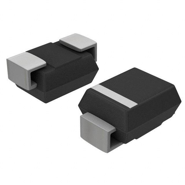
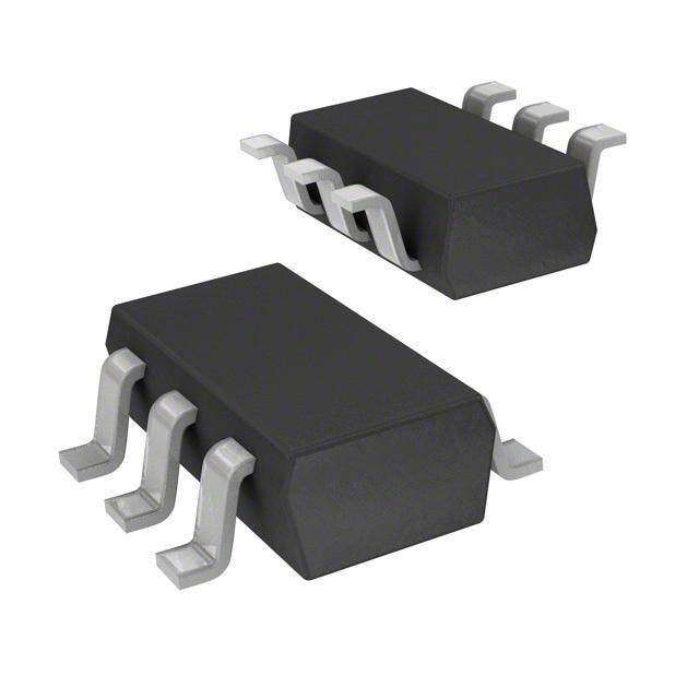
| 描述 | TVS DIODE 5VWM SOT666TVS二极管阵列 N Ch 30V 0.009 Ohm 40A Pwr MOSFET |
| 产品分类 | |
| 品牌 | STMicroelectronics |
| 产品手册 | |
| 产品图片 |
|
| rohs | 符合RoHS无铅 / 符合限制有害物质指令(RoHS)规范要求 |
| 产品系列 | 二极管与整流器,TVS二极管,TVS二极管阵列,STMicroelectronics ESDAULC6-3BP6ESDA |
| 数据手册 | |
| 产品型号 | ESDAULC6-3BP6 |
| 不同频率时的电容 | - |
| 产品目录页面 | |
| 产品种类 | TVS二极管阵列 |
| 供应商器件封装 | SOT-666 |
| 其它名称 | 497-7750-6 |
| 其它有关文件 | http://www.st.com/web/catalog/sense_power/FM114/CL1137/SC1767/PF182861?referrer=70071840http://www.st.com/web/catalog/sense_power/FM114/CL1137/SC492/SS1421/PF182861?referrer=70071840 |
| 击穿电压 | 9.2 V |
| 功率-峰值脉冲 | - |
| 包装 | Digi-Reel® |
| 单向通道 | - |
| 双向通道 | 3 |
| 商标 | STMicroelectronics |
| 外壳高度 | 0.6 mm |
| 安装类型 | 表面贴装 |
| 安装风格 | SMD/SMT |
| 封装 | Reel |
| 封装/外壳 | SOT-563,SOT-666 |
| 封装/箱体 | SOT-666 |
| 尺寸 | 1.3 mm W x 1.7 mm L x 0.6 mm H |
| 工作温度 | - |
| 工厂包装数量 | 3000 |
| 应用 | 通用 |
| 最大工作温度 | + 150 C |
| 最小工作温度 | - 55 C |
| 极性 | Bidirectional |
| 标准包装 | 1 |
| 电压-击穿(最小值) | 6V |
| 电压-反向关态(典型值) | 5V |
| 电压-箝位(最大值)@Ipp | - |
| 电容 | 1.5 pF |
| 电流-峰值脉冲(10/1000µs) | - |
| 电源线路保护 | 无 |
| 端接类型 | SMD/SMT |
| 类型 | 齐纳 |
| 系列 | ESDAULC6-3BP6 |
| 通道 | 3 Channels |


- 商务部:美国ITC正式对集成电路等产品启动337调查
- 曝三星4nm工艺存在良率问题 高通将骁龙8 Gen1或转产台积电
- 太阳诱电将投资9.5亿元在常州建新厂生产MLCC 预计2023年完工
- 英特尔发布欧洲新工厂建设计划 深化IDM 2.0 战略
- 台积电先进制程称霸业界 有大客户加持明年业绩稳了
- 达到5530亿美元!SIA预计今年全球半导体销售额将创下新高
- 英特尔拟将自动驾驶子公司Mobileye上市 估值或超500亿美元
- 三星加码芯片和SET,合并消费电子和移动部门,撤换高东真等 CEO
- 三星电子宣布重大人事变动 还合并消费电子和移动部门
- 海关总署:前11个月进口集成电路产品价值2.52万亿元 增长14.8%


PDF Datasheet 数据手册内容提取
ESDAULC6-3BP6 ESDAULC6-3BF2 ESD protection for high speed interface Main applications Where transient overvoltage protection in ESD sensitive equipment is required, such as: ■ Computers ■ Printers ■ Communication systems SOT-666 Flip-Chip ESDAULC6-3BP6 ESDAULC6-3BF2 ■ Cellular phones handsets and accessories ■ Video equipment Figure 1. Functional diagram Features A B ■ Ultra low capacitance 1.25 pF max. I/O1 1 6 GND I/O1 GND 1 ■ Bi-directional protection NC 2 5 NC ■ RoHS package I/O2 3 4 I/O3 I/O2 I/O3 2 Description Top view Bump side view ESDAULC6-3BP6 ESDAULC6-3BF2 The ESDAULC6-3Bxx is a monolithic application specific discrete device dedicated to ESD Figure 2. Pin configuration protection of high speed interfaces such as USB2.0. I/O1 I/O2 I/O3 The device is ideal for applications where both reduced print circuit board space and power absorption capability are required. Benefits GND ■ Ultra low capacitance bidirectional ESD T able 1. Order codes protection Part number Marking ■ Low PCB space consumption: 2.5 mm2 max footprint (1.7 mm2 for Flip-Chip) ESDAULC6-3BP6 3 ■ Enhanced ESD protection: ESDAULC6-3BF2 3B – 15 kV contact discharge Complies with the following standards: – 15 kV air discharge IEC 61000-4-2 level 4: ■ No insertion loss to 3.0 GHz 8 kV (contact discharge) ■ Ultra low leakage current 15 kV (air discharge) ■ High reliability offered by monolithic integration MIL STD 883G-Method 3015-7: class 3B HBM (Human Body Model) July 2007 Rev 1 1/11 www.st.com 11
Characteristics ESDAULC6-3BP6, ESDAULC6-3BF2 1 Characteristics T able 2. Absolute maximum ratings Symbol Parameter Value (min.) Unit IEC 61000-4-2 contact discharge 15 V Peak pulse voltage (1) kV PP IEC 61000-4-2 air discharge 15 T Maximum operating junction temperature 150 °C j T Storage temperature range -55 to +150 °C stg T Maximum lead temperature for soldering during 10 s at 5 mm for case 260 °C L 1. For a surge greater than the maximum values, the diode will fail in short-circuit. T able 3. Electrical characteristics (T = 25° C) amb Symbol Parameter I V Stand-off voltage RM V Breakdown voltage BR V Clamping voltage CL VCLVBR VRM I Leakage current V RM IRM VRMVBRVCL I Peak pulse current PP αT Voltage temperature coefficient C Capacitance Slope:1/Rd IPP R Dynamic resistance d Parameter Test condition Min Typ Max Unit V (1) I = 1 mA 6.0 9.2 V BR R I V = 5 V 0.5 µA RM RM R Square pulse, I = 6 A, t = 2.5 µs 1.4 Ω d PP p αT 1.2 10-4/°C V = 0 V, SOT-666 1.0 1.25 I/O F = 1 MHz, VOSC = 30 mV Flip-Chip 1.25 1.5 C pF i/o-i/o V = 1.65 V, V = 4.3 V, SOT-666 0.75 0.9 I/O CC F = 1 MHz, VOSC = 400 mV Flip-Chip 0.9 1.20 1. Same value for I/O to I/O and I/O to GND 2/11
ESDAULC6-3BP6, ESDAULC6-3BF2 Characteristics F igure 3. Relative variation of peak pulse Figure 4. Relative variation of peak pulse power versus initial junction power versus initial junction temperature (SOT-666) temperature (Flip-Chip) 1.1 PPP[Tjinitial] / PPP[Tjinitial=25°C) 1.1 PPP[Tjinitial]/PPP[Tjinitial=25°C] 1.0 1.0 0.9 0.9 0.8 0.8 0.7 0.7 0.6 0.6 0.5 0.5 0.4 0.4 0.3 0.3 0.2 0.2 0.1 Tj(°C) 0.1 Tj(°C) 0.0 0.0 0 25 50 75 100 125 150 0 25 50 75 100 125 150 Figure 5. P eak pulse power versus Figure 6. Peak pulse power versus exponential pulse duration exponential pulse duration (SOT-666) (Flip-Chip) PPP(W) 1000 1000 PPP(W) Tjinitial=25°C Tjinitial = 25°C 100 100 tp(µs) 10 tP(µs) 10 1 10 100 1 10 100 Figure 7. C lamping voltage versus peak Figure 8. Clamping voltage versus peak pulse current (typical values) pulse current (typical values) (SOT-666) (Flip-Chip) 10.0 IPP(A) 10.0 IPP(A) 8/20µs Square wave Tjinitial=25°C 2.5µs Tjinitial =25°C 1.0 1.0 VCL(V) VCL(V) 0.1 0.1 5 10 15 20 25 30 5 10 15 20 25 30 3/11
Characteristics ESDAULC6-3BP6, ESDAULC6-3BF2 Figure 9. J unction capacitance versus Figure 10. Junction capacitance versus reverse voltage applied (typical reverse voltage applied (typical values) (SOT-666) values) (Flip-Chip) C(pF) C(pF) 2 1 F=1MHz VOSFCT==j=132M05m°HCVzRMS VOSTC=j=3205m°CVRMS 1 VLINE(V) VLINE(V) 0 0 0 1 2 3 4 5 0 1 2 3 4 5 Figure 11. R elative variation of leakage Figure 12. Relative variation of leakage current versus junction current versus junction temperature (typical values) temperature (typical values) (SOT-666) (Flip-Chip) IR[Tj] / IR[Tj=25°C] IR[Tj]/IR[Tj=25°C] 100 100 VR=5V VR=5V 10 10 Tj(°C) Tj(°C) 1 1 25 50 75 100 125 150 25 50 75 100 125 Figure 13. R emaining voltage after Figure 14. Remaining voltage after ESDAULC6-3BP6 during ESD ESDAULC6-3BF2 during ESD 15 kV positive surge (air 15 kV positive surge (air discharge) (SOT-666) discharge) (Flip-Chip) V/div V/div 10 10 0.1 µs/div 0.1 µs/div 4/11
ESDAULC6-3BP6, ESDAULC6-3BF2 Characteristics F igure 15. Remaining voltage after Figure 16. Remaining voltage after ESDAULC6-3BP6 during ESD ESDAULC6-3BF2 during ESD 15 kV negative surge (air 15 kV negative surge (air discharge) (SOT-666) discharge) (Flip-Chip) v v di di V/ V/ 0 0 1 1 0.1 µs/div 0.1 µs/div Figure 17. S 21 attenuation measurement Figure 18. S21 attenuation measurement results of each channel (SOT-666) results of channel 1 (Flip-Chip) dB dB 0.00 0.00 -5.00 -5.00 -10.00 -10.00 -15.00 -15.00 F (Hz) F (Hz) -20.00 1.0M 3.0M 10.0M 30.0M 100.0M 300.0M 1.0G 3.0G -20.00 1.0M 3.0M 10.0M 30.0M 100.0M 300.0M 1.0G 3.0G Line 1 Line 2 Line 3 Line 1 Figure 19. A nalog crosstalk measurements Figure 20. Analog crosstalk measurements between channels (SOT-666) between channels (Flip-Chip) dB dB 0.00 0.00 -20.00 -20.00 -40.00 -40.00 -60.00 -60.00 -80.00 -80.00 -100.00 -100.00 -120.00 F (Hz) -120.00 F (Hz) -140.00 -140.00 1.0M 3.0M 10.0M 30.0M 100.0M 300.0M 1.0G 3.0G 1.0M 3.0M 10.0M 30.0M 100.0M 300.0M 1.0G 3.0G Xtalk 1/2 Xtalk 1/2 5/11
Application examples ESDAULC6-3BP6, ESDAULC6-3BF2 2 Application examples Figure 21. USB2.0 (high speed) protection application schematic R V O BUS T EC D+ N IC to Protect N O D- C 2.0 GND B S U Figure 22. Audio jack protection application schematic Audio jack 100pF FMTuner H n 0 3 3 Figure 23. SIM card protection application schematic OR RST T EC CLK SIM CARD N ON DATA PROCESSOR C RY GND O M E M 6/11
ESDAULC6-3BP6, ESDAULC6-3BF2 Ordering information scheme 3 Ordering information scheme ESDA ULC 6 - 3 B xx ESD Array Ultra low capacitance BreakdownVoltage 6 = 6Volts Number of lines protected 3 = 3 lines Type B = Bidirectional Packages F2 = Flip-Chip P6 = SOT-666 7/11
Package information ESDAULC6-3BP6, ESDAULC6-3BF2 4 Package information ● Epoxy meets UL 94, V0 T able 4. SOT-666 dimensions Dimensions b1 Ref. Millimeters Inches L1 Min. Typ. Max. Min. Typ. Max. A 0.45 0.60 0.018 0.024 L3 A3 0.08 0.18 0.003 0.007 b b 0.17 0.34 0.007 0.013 D E1 b1 0.19 0.27 0.34 0.007 0.011 0.013 D 1.50 1.70 0.059 0.067 A E 1.50 1.70 0.059 0.067 L2 E A3 E1 1.10 1.30 0.043 0.051 e 0.50 0.020 L1 0.19 0.007 L2 0.10 0.30 0.004 0.012 e L3 0.10 0.004 Figure 24. SOT-666 footprint (dimensions in mm) 0.50 0.62 2.60 0.99 0.30 8/11
ESDAULC6-3BP6, ESDAULC6-3BF2 Package information Figure 25. Flip-Chip dimensions 650 µm ± 65 500 µm ± 50 m µ m 1.0 mm ± 50 1.6 mm ± 50µ 1.1 mm ± 50 µm 315 µm ± 50 Figure 26. Flip-Chip footprint Figure 27. Flip-Chip marking Dot, ST logo Copper pad Diameter: xx = marking 220 µm recommended z = manufacturing location E yww = datecode So3ld3e0r µ smternecciol mopmeennindge:d (y = year x x z ww = week) Solder mask opening recommendation: y w w 300 µmrecommended Figure 28. Flip-Chip tape and reel specifications Dot identifying Pin A1 location Ø 1.5 +/- 0.1 4 +/- 0.1 1 .7 5 + /- 0 .1 3 .5 + 8 +/- 0.3 ywwxxzSTE ywwxxzSTE ywwxxzSTE /- 0.1 0.71 +/- 0.05 4 +/- 0.1 All dimensions in mm User direction of unreeling In order to meet environmental requirements, ST offers these devices in ECOPACK® packages. These packages have a lead-free second level interconnect. The category of second level interconnect is marked on the package and on the inner box label, in compliance with JEDEC Standard JESD97. The maximum ratings related to soldering conditions are also marked on the inner box label. ECOPACK is an ST trademark. ECOPACK specifications are available at: www.st.com. 9/11
Ordering information ESDAULC6-3BP6, ESDAULC6-3BF2 5 Ordering information T able 5. Ordering information Part number Marking Package Weight Base qty Delivery mode ESDAULC6-3BP6 3 SOT-666 2.9 mg 5000 Tape and reel ESDAULC6-3BF2 3B Flip-Chip 2.22 mg 5000 Tape and reel 6 Revision history T able 6. Revision history Datet Revision Changes 03-Jul-2007 1 Initial release 10/11
ESDAULC6-3BP6, ESDAULC6-3BF2 Please Read Carefully: Information in this document is provided solely in connection with ST products. STMicroelectronics NV and its subsidiaries (“ST”) reserve the right to make changes, corrections, modifications or improvements, to this document, and the products and services described herein at any time, without notice. All ST products are sold pursuant to ST’s terms and conditions of sale. Purchasers are solely responsible for the choice, selection and use of the ST products and services described herein, and ST assumes no liability whatsoever relating to the choice, selection or use of the ST products and services described herein. No license, express or implied, by estoppel or otherwise, to any intellectual property rights is granted under this document. If any part of this document refers to any third party products or services it shall not be deemed a license grant by ST for the use of such third party products or services, or any intellectual property contained therein or considered as a warranty covering the use in any manner whatsoever of such third party products or services or any intellectual property contained therein. UNLESS OTHERWISE SET FORTH IN ST’S TERMS AND CONDITIONS OF SALE ST DISCLAIMS ANY EXPRESS OR IMPLIED WARRANTY WITH RESPECT TO THE USE AND/OR SALE OF ST PRODUCTS INCLUDING WITHOUT LIMITATION IMPLIED WARRANTIES OF MERCHANTABILITY, FITNESS FOR A PARTICULAR PURPOSE (AND THEIR EQUIVALENTS UNDER THE LAWS OF ANY JURISDICTION), OR INFRINGEMENT OF ANY PATENT, COPYRIGHT OR OTHER INTELLECTUAL PROPERTY RIGHT. UNLESS EXPRESSLY APPROVED IN WRITING BY AN AUTHORIZED ST REPRESENTATIVE, ST PRODUCTS ARE NOT RECOMMENDED, AUTHORIZED OR WARRANTED FOR USE IN MILITARY, AIR CRAFT, SPACE, LIFE SAVING, OR LIFE SUSTAINING APPLICATIONS, NOR IN PRODUCTS OR SYSTEMS WHERE FAILURE OR MALFUNCTION MAY RESULT IN PERSONAL INJURY, DEATH, OR SEVERE PROPERTY OR ENVIRONMENTAL DAMAGE. ST PRODUCTS WHICH ARE NOT SPECIFIED AS "AUTOMOTIVE GRADE" MAY ONLY BE USED IN AUTOMOTIVE APPLICATIONS AT USER’S OWN RISK. Resale of ST products with provisions different from the statements and/or technical features set forth in this document shall immediately void any warranty granted by ST for the ST product or service described herein and shall not create or extend in any manner whatsoever, any liability of ST. ST and the ST logo are trademarks or registered trademarks of ST in various countries. Information in this document supersedes and replaces all information previously supplied. The ST logo is a registered trademark of STMicroelectronics. All other names are the property of their respective owners. © 2007 STMicroelectronics - All rights reserved STMicroelectronics group of companies Australia - Belgium - Brazil - Canada - China - Czech Republic - Finland - France - Germany - Hong Kong - India - Israel - Italy - Japan - Malaysia - Malta - Morocco - Singapore - Spain - Sweden - Switzerland - United Kingdom - United States of America www.st.com 11/11
Mouser Electronics Authorized Distributor Click to View Pricing, Inventory, Delivery & Lifecycle Information: S TMicroelectronics: ESDAULC6-3BP6 ESDAULC6-3BF2