
 Datasheet下载
- 型号: ESDA8V2-1MX2
- 制造商: STMicroelectronics
- 库位|库存: xxxx|xxxx
- 要求:
| 数量阶梯 | 香港交货 | 国内含税 |
| +xxxx | $xxxx | ¥xxxx |
查看当月历史价格
查看今年历史价格
ESDA8V2-1MX2产品简介:
ICGOO电子元器件商城为您提供ESDA8V2-1MX2由STMicroelectronics设计生产,在icgoo商城现货销售,并且可以通过原厂、代理商等渠道进行代购。 ESDA8V2-1MX2价格参考。STMicroelectronicsESDA8V2-1MX2封装/规格:TVS - 二极管, 。您可以下载ESDA8V2-1MX2参考资料、Datasheet数据手册功能说明书,资料中有ESDA8V2-1MX2 详细功能的应用电路图电压和使用方法及教程。
STMicroelectronics(意法半导体)的ESDA8V2-1MX2是一款TVS(瞬态电压抑制器)二极管,主要用于保护电子设备免受过电压瞬变的影响。以下是其主要应用场景:

 1. 数据线和信号线保护
   - ESDA8V2-1MX2适用于高速数据接口的保护,例如USB、HDMI、DisplayPort、以太网等。它能够有效抑制静电放电(ESD)、雷击感应浪涌和其他瞬态电压,确保信号完整性并防止损坏敏感的IC。

 2. 消费类电子产品
   - 在智能手机、平板电脑、笔记本电脑、电视和其他消费类电子产品中,该器件可用于保护电源输入端口、音频接口、摄像头模块等关键组件,提高产品的可靠性和耐用性。

 3. 工业自动化设备
   - 在工业环境中,该TVS二极管可用于保护传感器、控制器、通信模块(如RS-232、RS-485)以及电机驱动电路,防止因电磁干扰(EMI)或电气瞬变引起的故障。

 4. 汽车电子系统
   - 在汽车应用中,ESDA8V2-1MX2可以保护车载信息娱乐系统、导航模块、CAN总线和LIN总线等免受高压瞬变的影响,满足汽车级的严格要求。

 5. 通信设备
   - 在路由器、交换机、基站和其他通信设备中,该器件可用于保护天线接口、射频模块和控制电路,确保设备在恶劣环境下的稳定运行。

 6. 医疗设备
   - 在医疗仪器中,如心率监测仪、超声波设备等,该TVS二极管可保护关键电路免受ESD和浪涌冲击,保障设备的安全性和准确性。

 特点总结:
- 低电容设计:适合高速信号线路。
- 高浪涌能力:能够承受多次重复的瞬态电压冲击。
- 快速响应时间:有效抑制瞬态电压,保护下游电路。
- 小封装尺寸:便于在空间受限的设计中使用。

通过这些应用场景,ESDA8V2-1MX2为各种电子设备提供了可靠的过电压保护解决方案。
| 参数 | 数值 |
| 产品目录 | |
| 描述 | TVS DIODE 5VWM 18.5VC 2QFNTVS 二极管 - 瞬态电压抑制器 EOS AND ESD TRANSIL |
| 产品分类 | |
| 品牌 | STMicroelectronics |
| 产品手册 | |
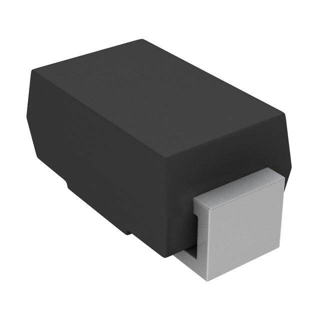
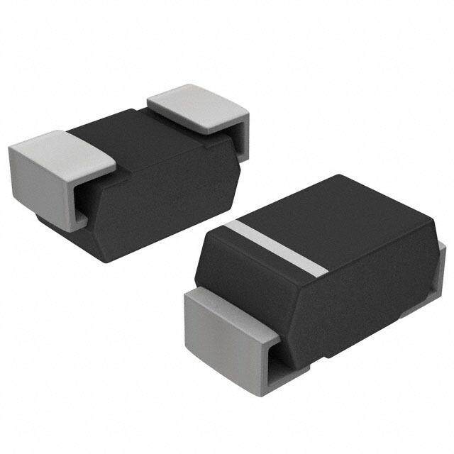
| 产品图片 |
|
| rohs | 符合RoHS无铅 / 符合限制有害物质指令(RoHS)规范要求 |
| 产品系列 | 二极管与整流器,TVS二极管,TVS 二极管 - 瞬态电压抑制器,STMicroelectronics ESDA8V2-1MX2ESDA, TRANSIL™ |
| 数据手册 | |
| 产品型号 | ESDA8V2-1MX2 |
| 不同频率时的电容 | 350pF @ 1MHz |
| 产品种类 | TVS 二极管 - 瞬态电压抑制器 |
| 供应商器件封装 | 2-µQFN (1.45x1.0) |
| 其它名称 | 497-10588-1 |
| 其它有关文件 | http://www.st.com/web/catalog/sense_power/FM114/CL1137/SC492/PF217523?referrer=70071840http://www.st.com/web/catalog/sense_power/FM114/CL1137/SC492/SS1421/PF217523?referrer=70071840 |
| 击穿电压 | 8.2 V |
| 功率-峰值脉冲 | 500W |
| 包装 | 剪切带 (CT) |
| 单向通道 | 1 |
| 双向通道 | - |
| 商标 | STMicroelectronics |
| 商标名 | Transil |
| 安装类型 | 表面贴装 |
| 安装风格 | SMD/SMT |
| 封装 | Reel |
| 封装/外壳 | 2-UFDFN |
| 封装/箱体 | UQFN-2L |
| 尺寸 | 1 mm W x 1.45 mm L x 0.55 mm H |
| 峰值浪涌电流 | 27 A |
| 峰值脉冲功率耗散 | 500 W |
| 工作温度 | -40°C ~ 125°C (TJ) |
| 工厂包装数量 | 3000 |
| 应用 | 通用 |
| 最大工作温度 | + 125 C |
| 最小工作温度 | - 40 C |
| 极性 | Unidirectional |
| 标准包装 | 1 |
| 特色产品 | http://www.digikey.com/cn/zh/ph/st/ESDA8V2.html |
| 电压-击穿(最小值) | 8.2V |
| 电压-反向关态(典型值) | 5V |
| 电压-箝位(最大值)@Ipp | 18.5V |
| 电容 | 350 pF |
| 电流-峰值脉冲(10/1000µs) | 27A (8/20µs) |
| 电源线路保护 | 无 |
| 端接类型 | SMD/SMT |
| 类型 | 齐纳 |
| 系列 | ESDA8V2-1MX2 |
| 钳位电压 | 12 V, 13 V, 18.5 V |


- 商务部:美国ITC正式对集成电路等产品启动337调查
- 曝三星4nm工艺存在良率问题 高通将骁龙8 Gen1或转产台积电
- 太阳诱电将投资9.5亿元在常州建新厂生产MLCC 预计2023年完工
- 英特尔发布欧洲新工厂建设计划 深化IDM 2.0 战略
- 台积电先进制程称霸业界 有大客户加持明年业绩稳了
- 达到5530亿美元!SIA预计今年全球半导体销售额将创下新高
- 英特尔拟将自动驾驶子公司Mobileye上市 估值或超500亿美元
- 三星加码芯片和SET,合并消费电子和移动部门,撤换高东真等 CEO
- 三星电子宣布重大人事变动 还合并消费电子和移动部门
- 海关总署:前11个月进口集成电路产品价值2.52万亿元 增长14.8%


PDF Datasheet 数据手册内容提取
ESDA8V2-1MX2 EOS and ESD Transil™ protection for charger and battery port Features ■ Breakdown voltage V = 8.2 V BR ■ Unidirectional device ■ High peak power dissipation: 500 W (8/20 µs waveform) ■ ESD protection level better than IEC 61000-4-2, level 4: 30 kV contact discharge ■ Low leakage current (< 0.5 µA @ 5 V) µQFN 2L package ■ Very small PCB area (1.45 mm2) ■ RoHS compliant Figure 1. Functional diagram (top view) Benefits ■ High EOS and ESD protection level ■ High integration ■ Suitable for high density boards ■ Tiny package Complies with the following standards: ■ IEC 61000-4-2 level 4 – ±15 kV (air discharge) – ±8 kV (contact discharge) ■ MIL STD 883G - Method 3015-7: class 3B – HBM (human body model): ≥8kV Description Applications The ESDA8V2-1MX2 is a unidirectional single line Where EOS and ESD transient overvoltage Transil diode designed specifically for the protection in sensitive equipment is required, protection of integrated circuits in portable such as: equipment and miniaturized electonic devices subject to EOS and ESD transient overvoltages. ■ Computers ■ Printers ■ Communication systems ■ Cellular phone handsets and accessories ■ Video equipment TM: Transil is a trademark of STMicroelectronics August 2008 Rev 1 1/10 www.st.com
Characteristics ESDA8V2-1MX2 1 Characteristics Table 1. A b solute maximum ratings (T = 25 °C) amb Symbol Parameter Value Unit ESD discharge: IEC 61000-4-2 air discharge on input pin ±30 V kV PP IEC 61000-4-2 contact discharge on input pin ±30 MIL STD 883G - Method 3015-7: class 3B ±30 P Peak pulse power dissipation (8/20 µs) (1) T = T 500 W PP j initial amb I Peak pulse current (8/20 µs) 27 A PP T Junction temperature range -40 to +125 °C j T Storage temperature range - 55 to +150 °C stg T Maximum lead temperature for soldering during 10 s 260 °C L 1. For a surge greater than the maximum values, the diode will fail in short-circuit Table 2. E lectrical characteristics (definitions) Symbol Parameter I VBR Breakdown voltage IF I Leakage current @ V RM RM VRM Stand-of voltage VCLVBRVRM VF VVVVVV V Clamping voltage IRM CL IR I Peak pulse current PP Slope= 1/Rd Cline Input line capacitance IPP Table 3. E lectrical characteristics (values, T = 25 °C) amb Symbol Test Condition Min Typ Max Unit V I = 1 mA 8.2 V BR R I V = 5 V 0.1 0.5 µA RM RM I = 1 A (8/20 µs waveform) 12 V PP V I = 5 A (8/20 µs waveform) 13 V CL PP I = 27 A (8/20 µs waveform) 18.5 V pp C V = 0 V, F = 1 MHz, V = 30 mV 350 430 pF line R osc osc 2/10
ESDA8V2-1MX2 Characteristics Figure 2. R elative variation of peak pulse Figure 3. Peak pulse power versus power versus initial junction exponential pulse duration temperature (typical values) (8/20 µs, typical values) Figure 4. C lamping voltage versus peak Figure 5. Forward voltage drop versus peak pulse current forward current (typical values) (8/20 µs, typical values) Figure 6. Junction capacitance versus reverse voltage applied (typical values) 3/10
Ordering information scheme ESDA8V2-1MX2 Figure 7. E SD response to IEC 61000-4-2 Figure 8. ESD response to IEC 61000-4-2 (+30 kV air discharge) (-30 kV air discharge) 2 Ordering information scheme Figure 9. Ordering information scheme 4/10
ESDA8V2-1MX2 Package information 3 Package information ● Epoxy meets UL94, V0 In order to meet environmental requirements, ST offers these devices in ECOPACK® packages. These packages have a lead-free second level interconnect. The category of second level interconnect is marked on the inner box label, in compliance with JEDEC Standard JESD97. The maximum ratings related to soldering conditions are also marked on the inner box label. ECOPACK is an ST trademark. ECOPACK specifications are available at www.st.com. T able 4. µQFN 2L dimensions Dimensions Ref Millimetres Inches Min Typ Max Min Typ Max A 0.51 0.55 0.60 0.020 0.022 0.024 A1 0.00 0.02 0.05 0.000 0.001 0.002 b1 0.25 0.30 0.35 0.010 0.012 0.014 D 1.45 0.057 E 1.00 0.039 e 0.95 1.00 1.05 0.037 0.039 0.041 L1 0.75 0.80 0.85 0.030 0.031 0.033 F igure 10. Footprint (dimensions in mm) Figure 11. Marking Note: Product marking may be rotated by 90° for assembly plant differentiation. In no case should this product marking be used to orient the component for its placement on a PCB. Only pin 1 mark is to be used for this purpose. 5/10
Package information ESDA8V2-1MX2 Figure 12. Tape and reel specifications 6/10
ESDA8V2-1MX2 Recommendation on PCB assembly 4 Recommendation on PCB assembly 4.1 Stencil opening design 1. General recommendation on stencil opening design a) Stencil opening dimensions: L (Length), W (Width), T (Thickness). Figure 13. Stencil opening dimensions L T W b) General design rule Stencil thickness (T) = 75 ~ 125 µm W Aspect Ratio = -----≥1.5 T L×W Aspect Area = ----------------------------≥0.66 2T(L+W) 2. Reference design a) Stencil opening thickness: 100 µm b) Stencil opening for leads: Opening to footprint ratio - between 40% and 50%. Figure 14. Recommended stencil windows position T=100µm 95µm 95µm 0.0.62 135µm 0.83 m µ m µ 0 3 0 8 6 5 0.55 360µm 1.72 135µm Footprint 550µm Stencilwindow Footprint 7/10
Recommendation on PCB assembly ESDA8V2-1MX2 4.2 Solder paste 1. Halide-free flux qualification ROL0 according to ANSI/J-STD-004. 2. “No clean” solder paste is recommended. 3. Offers a high tack force to resist component movement during high speed 4. Solder paste with fine particles: powder particle size is 20-45 µm. 4.3 Placement 1. Manual positioning is not recommended. 2. It is recommended to use the lead recognition capabilities of the placement system, not the outline centering 3. Standard tolerance of ± 0.05 mm is recommended. 4. 3.5 N placement force is recommended. Too much placement force can lead to squeezed out solder paste and cause solder joints to short. Too low placement force can lead to insufficient contact between package and solder paste that could cause open solder joints or badly centered packages. 5. To improve the package placement accuracy, a bottom side optical control should be performed with a high resolution tool. 6. For assembly, a perfect supporting of the PCB (all the more on flexible PCB) is recommended during solder paste printing, pick and place and reflow soldering by using optimized tools. 4.4 PCB design preference 1. To control the solder paste amount, the closed via is recommended instead of open vias. 2. The position of tracks and open vias in the solder area should be well balanced. The symmetrical layout is recommended, in case any tilt phenomena caused by asymmetrical solder paste amount due to the solder flow away. 8/10
ESDA8V2-1MX2 Ordering information 4.5 Reflow profile Figure 15. ST ECOPACK® recommended soldering reflow profile for PCB mounting TTeemmppeerraattuurree ((°°CC)) 226600°°CC mmaaxx 225555°°CC 222200°°CC 118800°°CC 112255 °°CC 2°C/s 2r°eCc/osm remceonmdmedended 3°C/s max 6°C/s max 6°C/s max 3°C/s max 00 00 11 22 33 44 55 66 77 1100--3300 sseecc TTiimmee ((mmiinn)) 9900 ttoo 115500 sseecc 9900 sseecc mmaaxx Note: Minimize air convection currents in the reflow oven to avoid component movement. 5 Ordering information T able 5. Ordering information Order code Marking Weight Base qty Delivery mode ESDA8V2-1MX2 Y(1) 2.9 mg 3000 Tape and reel 1. The marking can be rotated by 90° to diferentiate assembly location 6 Revision history T able 6. Document revision history Date Revision Changes 27-Aug-2008 1 Initial release 9/10
ESDA8V2-1MX2 Please Read Carefully: Information in this document is provided solely in connection with ST products. STMicroelectronics NV and its subsidiaries (“ST”) reserve the right to make changes, corrections, modifications or improvements, to this document, and the products and services described herein at any time, without notice. All ST products are sold pursuant to ST’s terms and conditions of sale. Purchasers are solely responsible for the choice, selection and use of the ST products and services described herein, and ST assumes no liability whatsoever relating to the choice, selection or use of the ST products and services described herein. No license, express or implied, by estoppel or otherwise, to any intellectual property rights is granted under this document. If any part of this document refers to any third party products or services it shall not be deemed a license grant by ST for the use of such third party products or services, or any intellectual property contained therein or considered as a warranty covering the use in any manner whatsoever of such third party products or services or any intellectual property contained therein. UNLESS OTHERWISE SET FORTH IN ST’S TERMS AND CONDITIONS OF SALE ST DISCLAIMS ANY EXPRESS OR IMPLIED WARRANTY WITH RESPECT TO THE USE AND/OR SALE OF ST PRODUCTS INCLUDING WITHOUT LIMITATION IMPLIED WARRANTIES OF MERCHANTABILITY, FITNESS FOR A PARTICULAR PURPOSE (AND THEIR EQUIVALENTS UNDER THE LAWS OF ANY JURISDICTION), OR INFRINGEMENT OF ANY PATENT, COPYRIGHT OR OTHER INTELLECTUAL PROPERTY RIGHT. UNLESS EXPRESSLY APPROVED IN WRITING BY AN AUTHORIZED ST REPRESENTATIVE, ST PRODUCTS ARE NOT RECOMMENDED, AUTHORIZED OR WARRANTED FOR USE IN MILITARY, AIR CRAFT, SPACE, LIFE SAVING, OR LIFE SUSTAINING APPLICATIONS, NOR IN PRODUCTS OR SYSTEMS WHERE FAILURE OR MALFUNCTION MAY RESULT IN PERSONAL INJURY, DEATH, OR SEVERE PROPERTY OR ENVIRONMENTAL DAMAGE. ST PRODUCTS WHICH ARE NOT SPECIFIED AS "AUTOMOTIVE GRADE" MAY ONLY BE USED IN AUTOMOTIVE APPLICATIONS AT USER’S OWN RISK. Resale of ST products with provisions different from the statements and/or technical features set forth in this document shall immediately void any warranty granted by ST for the ST product or service described herein and shall not create or extend in any manner whatsoever, any liability of ST. ST and the ST logo are trademarks or registered trademarks of ST in various countries. Information in this document supersedes and replaces all information previously supplied. The ST logo is a registered trademark of STMicroelectronics. All other names are the property of their respective owners. © 2008 STMicroelectronics - All rights reserved STMicroelectronics group of companies Australia - Belgium - Brazil - Canada - China - Czech Republic - Finland - France - Germany - Hong Kong - India - Israel - Italy - Japan - Malaysia - Malta - Morocco - Singapore - Spain - Sweden - Switzerland - United Kingdom - United States of America www.st.com 10/10
Mouser Electronics Authorized Distributor Click to View Pricing, Inventory, Delivery & Lifecycle Information: S TMicroelectronics: ESDA8V2-1MX2