
 Datasheet下载
- 型号: SR70.TCT
- 制造商: SEMTECH
- 库位|库存: xxxx|xxxx
- 要求:
| 数量阶梯 | 香港交货 | 国内含税 |
| +xxxx | $xxxx | ¥xxxx |
查看当月历史价格
查看今年历史价格
SR70.TCT产品简介:
ICGOO电子元器件商城为您提供SR70.TCT由SEMTECH设计生产,在icgoo商城现货销售,并且可以通过原厂、代理商等渠道进行代购。 SR70.TCT价格参考。SEMTECHSR70.TCT封装/规格:TVS - 二极管, 。您可以下载SR70.TCT参考资料、Datasheet数据手册功能说明书,资料中有SR70.TCT 详细功能的应用电路图电压和使用方法及教程。
Semtech Corporation的SR70.TCT是一款瞬态电压抑制(TVS)二极管,主要用于保护电子设备免受过电压事件的影响。以下是该型号的应用场景:

1. 通信设备:在有线和无线通信系统中,SR70.TCT可用于保护接口电路(如RS-232、USB、以太网等)免受静电放电(ESD)、雷击浪涌和其他瞬态电压的损害。

2. 消费类电子产品:例如电视、音响系统、家用电器等,SR70.TCT可以保护敏感的集成电路和信号线路,确保设备在恶劣环境下仍能正常工作。

3. 工业自动化:在工业控制设备、传感器和数据采集系统中,该器件能够保护输入输出端口不受瞬态电压影响,提高系统的可靠性和稳定性。

4. 汽车电子:适用于车载电子系统,如信息娱乐系统、导航设备和车身控制系统,防止因负载突变或电气干扰导致的损坏。

5. 电源管理:在开关电源、电池充电器和其他电源转换电路中,SR70.TCT可提供过电压保护,避免因电压波动引起的故障。

6. 物联网(IoT)设备:在智能家庭、可穿戴设备和其他低功耗设备中,该器件有助于保护小型化电路免受外部干扰。

总之,SR70.TCT凭借其快速响应时间和低箝位电压特性,成为众多电子设备中不可或缺的保护元件,广泛应用于需要高可靠性、高性能保护的场合。
| 参数 | 数值 |
| 产品目录 | |
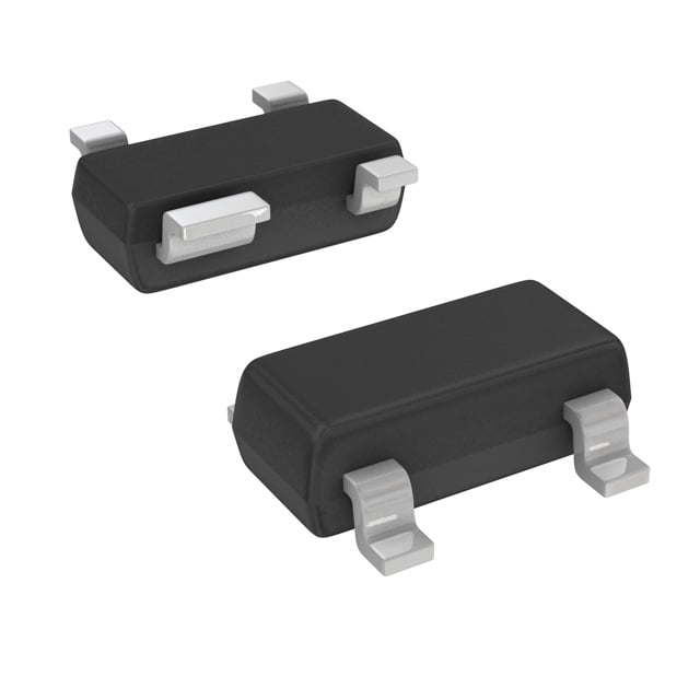
| 描述 | TVS DIODE 70VWM 7VC SOT143 |
| 产品分类 | |
| 品牌 | Semtech |
| 数据手册 | |
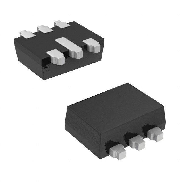
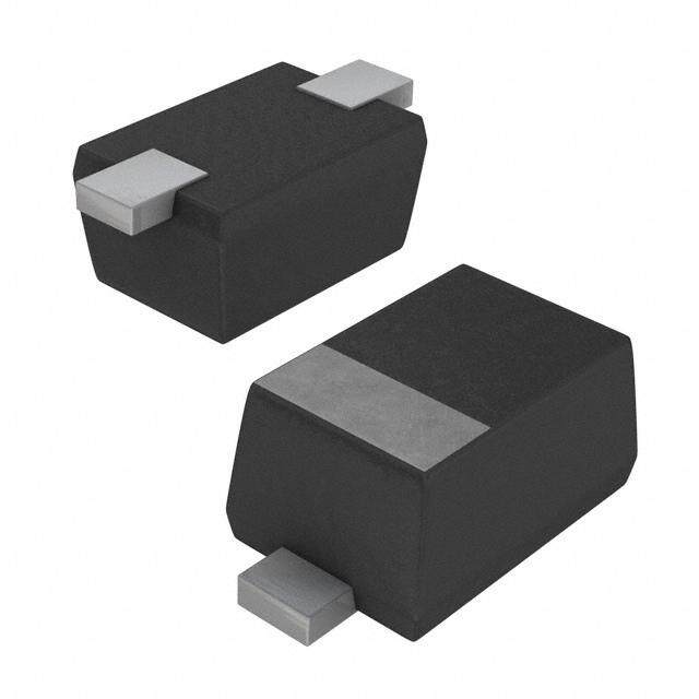
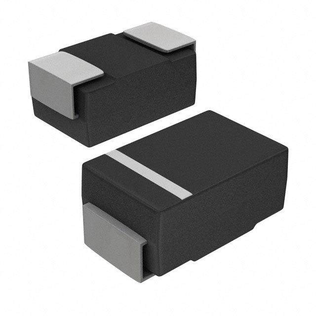
| 产品图片 |
|
| 产品型号 | SR70.TCT |
| rohs | 无铅 / 符合限制有害物质指令(RoHS)规范要求 |
| 产品系列 | RailClamp® |
| 不同频率时的电容 | 5pF @ 1MHz |
| 产品目录页面 | |
| 供应商器件封装 | SOT-143 |
| 其它名称 | SR70DKR |
| 功率-峰值脉冲 | - |
| 包装 | Digi-Reel® |
| 单向通道 | - |
| 双向通道 | 2 |
| 安装类型 | 表面贴装 |
| 封装/外壳 | TO-253-4,TO-253AA |
| 工作温度 | -55°C ~ 125°C (TJ) |
| 应用 | 通用 |
| 标准包装 | 1 |
| 电压-击穿(最小值) | 85V |
| 电压-反向关态(典型值) | 70V (最小值) |
| 电压-箝位(最大值)@Ipp | 7V |
| 电流-峰值脉冲(10/1000µs) | 24A (8/20µs) |
| 电源线路保护 | 无 |
| 类型 | 转向装置(轨至轨) |


- 商务部:美国ITC正式对集成电路等产品启动337调查
- 曝三星4nm工艺存在良率问题 高通将骁龙8 Gen1或转产台积电
- 太阳诱电将投资9.5亿元在常州建新厂生产MLCC 预计2023年完工
- 英特尔发布欧洲新工厂建设计划 深化IDM 2.0 战略
- 台积电先进制程称霸业界 有大客户加持明年业绩稳了
- 达到5530亿美元!SIA预计今年全球半导体销售额将创下新高
- 英特尔拟将自动驾驶子公司Mobileye上市 估值或超500亿美元
- 三星加码芯片和SET,合并消费电子和移动部门,撤换高东真等 CEO
- 三星电子宣布重大人事变动 还合并消费电子和移动部门
- 海关总署:前11个月进口集成电路产品价值2.52万亿元 增长14.8%


PDF Datasheet 数据手册内容提取
SR70 RailClamp Low Capacitance TVS Diode Array PROTECTION PRODUCTS - RailClamp Description Features RailClamps are surge rated diode arrays designed to (cid:139) Transient protection for high speed data lines to protect high speed data interfaces. The SR70 has IEC 61000-4-2 (ESD) ±15kV (air), ±8kV (contact) been specifically designed to protect sensitive compo- IEC 61000-4-4 (EFT) 40A (5/50ns) nents which are connected to data and transmission IEC 61000-4-5 (Lightning) 1kV, 24A (8/20µs) lines from over-voltages caused by electrostatic (cid:139) Array of surge rated, low capacitance diodes discharge (ESD), electrical fast transients (EFT), and (cid:139) Protects two I/O lines lightning. The SR70 has been optimized for use on (cid:139) Low capacitance (5pF typical) for high-speed ADSL and other high-speed interfaces. interfaces The unique design of the SR70 integrates four surge (cid:139) Low clamping voltage rated, low capacitance steering diodes in a low profile (cid:139) Solid-state silicon-avalanche technology SOT-143 package. It has a typical capacitance of only 5pF and may be used to protect two high-speed lines Mechanical Characteristics without sacrificing signal integrity. The SR70 is de- (cid:139) JEDEC SOT-143 package signed to replace “standard” rectifiers that are not (cid:139) UL 497B listed rated for the high energy surges that are normally (cid:139) Molding compound flammability rating: UL 94V-0 expected in telecommunications applications. (cid:139) Marking: R70 During transient conditions, the steering diodes direct (cid:139) Packaging: Tape and Reel per EIA 481 the transient to either the positive side of the power supply line or to ground. The maximum clamping Applications voltage seen by the protected circuit will be one diode drop (V ) above the supply (reference) voltage. The (cid:139) ADSL Lines F SR70 may be used as a stand alone device or in (cid:139) I2C Bus Protection conjunction with TVS diodes for enhanced protection. (cid:139) Video Line Protection (cid:139) T1/E1 secondary IC Side Protection (cid:139) Portable Electronics (cid:139) Microcontroller Input Protection (cid:139) WAN/LAN Equipment (cid:139) ISDN S/T Interface Circuit Diagram Schematic & PIN Configuration Pin 4 4 1 Pin 2 Pin 3 2 3 Pin 1 SOT-143 (Top View) Revision 03/03/06 1 www.semtech.com
SR70 PROTECTION PRODUCTS Absolute Maximum Rating Rating Symbol Value Units PeakPulseCurrent (t =8/20µs) I 24 A p PP RectifierRepetitivePeakReverseVoltage V 70 V RRM ESDperIEC61000-4-2(Air) V 15 kV ESD ESDperIEC61000-4-2(Contact) 8 Lead Soldering Temperature T 260(10sec.) °C L Operating Temperature T -55to+125 °C J StorageTemperature T -55to+150 °C STG Electrical Characteristics (T=25oC) SR70 Parameter Symbol Conditions Minimum Typical Maximum Units PeakReverseStand-Off Voltage V 70 V RRM ReverseBreakdown Voltage V I = 50µA 85 V BR t ReverseLeakageCurrent I V = 70V, T=25°C 5 µA R RWM Forward Clamping Voltage V I = 1A, t = 8/20µs 1.5 V FC PP p Forward Clamping Voltage V I = 10A, t = 8/20µs 3.3 V FC PP p Forward Clamping Voltage V I = 24A, t = 8/20µs 7 V FC PP p Junction Capacitance C Between I/O pinsand 5 10 pF j Ground V = 0V, f = 1MHz R Between I/O pins 3 pF V = 0V, f = 1MHz R 2006 Semtech Corp. 2 www.semtech.com
SR70 PROTECTION PRODUCTS Typical Characteristics Non-Repetitive Peak Pulse Power vs. Pulse Time Power Derating Curve 10 110 100 W) 90 wer - P (kPk 1 Power or IPP 678000 ak Pulse Po 0.1 % of Rated 345000 Pe 20 10 0.01 0 0.1 1 10 100 1000 0 25 50 75 100 125 150 Pulse Duration - tp (µs) Ambient Temperature - TA (oC) Pulse Waveform Capacitance vs. Reverse Voltage 110 0 100 Waveform I/O to GND Parameters: -2 f = 1MHz 90 tr = 8µs e 80 td = 20µs anc -4 nt of IPP 6700 e-t n Capacit --86 ce 50 e i Per 40 td = IPP/2 hang -10 30 % C -12 20 -14 10 0 -16 0 5 10 15 20 25 30 0 1 2 3 4 5 6 Time (µs) Reverse Voltage - VR (V) Forward Voltage vs. Forward Current 10 9 8 V) (F 7 V e - 6 g olta 5 V d 4 ar w 3 or Waveform F 2 Parameters: tr = 8µs 1 td = 20µs 0 0 5 10 15 20 25 30 35 40 45 50 Forward Current - IF (A) 2006 Semtech Corp. 3 www.semtech.com
SR70 PROTECTION PRODUCTS Applications Information SR70 Pin Configuration Device Connection Options for Protection of Two High-Speed Data Lines The SR70 is designed to protect two data lines from transient over-voltages by clamping them to a fixed reference. When the voltage on the protected line 4 1 exceeds the reference voltage (plus diode V ) the F steering diodes are forward biased, conducting the transient current away from the sensitive circuitry. Data lines are connected at pins 2 and 3. The nega- tive reference (REF1) is connected at pin 1. This pin should be connected directly to a ground plane on the board for best results. The path length is kept as short 2 3 as possible to minimize parasitic inductance. The positive reference (REF2) is connected at pin 4. The options for connecting the positive reference are as follows: 1. To protect data lines and the power line, connect Data Line and Power Supply Protection Using Vcc as pins 2 and 3 directly to the positive supply rail (V ). reference CC In this configuration the data lines are referenced to the supply voltage. An external TVS diode may be added between the supply rail and ground in order to prevent over-voltage on the supply rail. 2. In applications where no positive supply reference is available, or complete supply isolation is desired, an external TVS diode may be used as the refer- ence. The steering diodes will begin to conduct when the voltage on the protected line exceeds the working voltage of the TVS (plus one diode drop). Matte Tin Lead Finish Matte tin has become the industry standard lead-free replacement for SnPb lead finishes. A matte tin finish is composed of 100% tin solder with large grains. Since the solder volume on the leads is small com- pared to the solder paste volume that is placed on the land pattern of the PCB, the reflow profile will be determined by the requirements of the solder paste. Therefore, these devices are compatible with both lead-free and SnPb assembly techniques. In addition, unlike other lead-free compositions, matte tin does not have any added alloys that can cause degradation of the solder joint. 2006 Semtech Corp. 4 www.semtech.com
SR70 PROTECTION PRODUCTS Outline Drawing - SOT-143 D A e H DIMENSIONS e/2 DIM INCHES MILLIMETERS MINNOMMAX MINNOMMAX 4 3 GAUGE 0 c A .031 - .048 0.80 - 1.22 B SEATING PLANE A1 .000 - .006 0.013 - 0.15 PLANE A2 .029 .035 .042 0.75 0.90 1.07 0.25 b .011 - .020 0.30 - 0.51 C b1 .029 - .037 0.76 - 0.94 L c .003 - .008 0.08 - 0.20 L1 D .110 .114 .120 2.80 2.90 3.04 E1 E DETAIL A E .082 .093 .104 2.10 2.37 2.64 E1 .047 .051 .055 1.20 1.30 1.40 e .075 1.92 BSC e1 .008 0.20 BSC L .015 .020 .024 0.40 0.50 0.60 L1 (.021) (0.54) 1 2 N0 0° 4- 8° 0° 4- 8° aaa .006 0.15 e1 bxN bbb .008 0.20 bbb C A B SIDE VIEW SEE DETAIL A ccc .004 0.10 A2 A 4X ccc C SEATING PLANE b1 A1 C aaa C A B NOTES: 1. CONTROLLING DIMENSIONS ARE IN MILLIMETERS (ANGLES IN DEGREES). 2. DATUMS - A - AND - B - TO BE DETERMINED AT DATUM PLANE-H- 3. DIMENSIONS "E1" AND "D" DO NOT INCLUDE MOLD FLASH, PROTRUSIONS OR GATE BURRS. 4. REFERENCE JEDEC STD TO-253, VARIATION D. Land Pattern - SOT-143 X1 X1 Y DIMENSIONS DIM INCHES MILLIMETERS C (.087) (2.20) Z E1 C G E1 .076 1.92 E2 E2 .068 1.72 G .031 0.80 X1 .039 1.00 X2 .047 1.20 Y .055 1.40 Y Z .141 3.60 X2 X1 NOTES: 1. THIS LAND PATTERN IS FOR REFERENCE PURPOSES ONLY CONSULT YOUR MANUFACTURING GROUP TO ENSURE YOUR COMPANY'S MANUFACTURING GUIDELINES ARE MET. 2. REFERENCE IPC-SM-782A. 2006 Semtech Corp. 5 www.semtech.com
SR70 PROTECTION PRODUCTS Marking Codes Marking Part Number Code SR70 R70 R70 SR70 Marking (Top View) Ordering Information Part Qtyper Lead Finish ReelSize Number Reel SR70.TC SnPb 3,000 7Inch SR70.TCT Pb Free 3,000 7Inch Lead-free version is RoHS/WEEE Compliant Contact Information Semtech Corporation Protection Products Division 200 Flynn Rd., Camarillo, CA 93012 Phone: (805)498-2111 FAX (805)498-3804 2006 Semtech Corp. 6 www.semtech.com