ICGOO在线商城 > 集成电路(IC) > 嵌入式 - FPGA(现场可编程门阵列) > EP4CE40U19I7N
 Datasheet下载
- 型号: EP4CE40U19I7N
- 制造商: altera
- 库位|库存: xxxx|xxxx
- 要求:
| 数量阶梯 | 香港交货 | 国内含税 |
| +xxxx | $xxxx | ¥xxxx |
查看当月历史价格
查看今年历史价格
EP4CE40U19I7N产品简介:
ICGOO电子元器件商城为您提供EP4CE40U19I7N由altera设计生产,在icgoo商城现货销售,并且可以通过原厂、代理商等渠道进行代购。 EP4CE40U19I7N价格参考。alteraEP4CE40U19I7N封装/规格:嵌入式 - FPGA(现场可编程门阵列), 。您可以下载EP4CE40U19I7N参考资料、Datasheet数据手册功能说明书,资料中有EP4CE40U19I7N 详细功能的应用电路图电压和使用方法及教程。
Intel(原Altera)EP4CE40U19I7N 是一款基于Cyclone IV系列的FPGA(现场可编程门阵列)芯片,广泛应用于需要高性能、高灵活性和低功耗的嵌入式系统中。其主要应用场景包括:

1. 工业控制与自动化:用于实现复杂的控制逻辑、运动控制、传感器接口与数据采集系统,支持实时响应和高可靠性。

2. 通信设备:适用于通信协议转换、信号处理、网络交换、无线基站中的数据处理与接口逻辑控制。

3. 视频与图像处理:可用于视频采集、图像处理、编码/解码(如HDMI、SDI接口处理),支持实时图像增强与分析。

4. 汽车电子:用于车载显示系统、摄像头接口处理、ADAS(高级驾驶辅助系统)中的传感器融合逻辑实现。

5. 测试与测量设备:作为核心处理单元,实现高速数据采集、波形生成与实时分析功能。

6. 消费电子:在需要定制化逻辑与接口控制的产品中,如智能家电、可穿戴设备中进行功能扩展与系统整合。

该FPGA具备丰富的逻辑单元、嵌入式存储器、PLL资源和高速I/O,适合多种中高端嵌入式应用场景,支持用户灵活定制硬件功能。
| 参数 | 数值 |
| 产品目录 | 集成电路 (IC)半导体 |
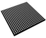
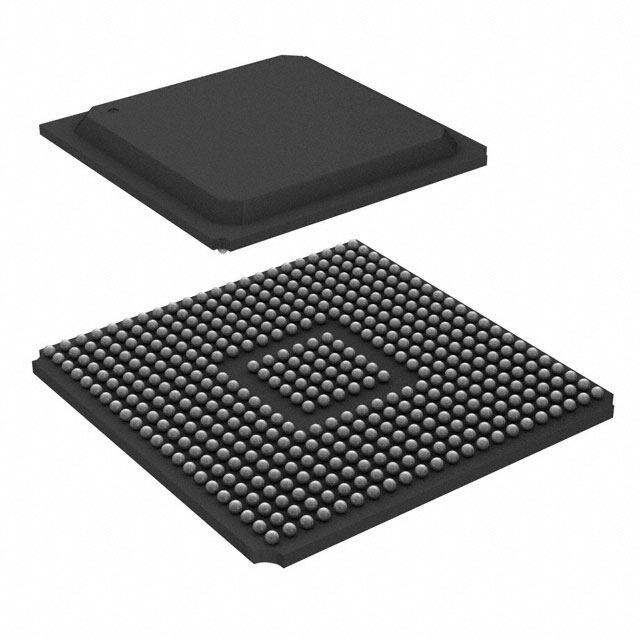
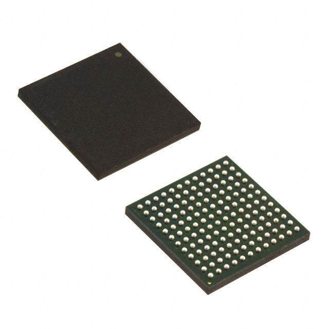
| 描述 | IC FPGA 328 I/O 484UBGAFPGA - 现场可编程门阵列 FPGA - Cyclone IV E 2475 LABs 328 IOs |
| 产品分类 | |
| I/O数 | 328 |
| LAB/CLB数 | 2475 |
| 品牌 | Altera Corporation |
| 产品手册 | |
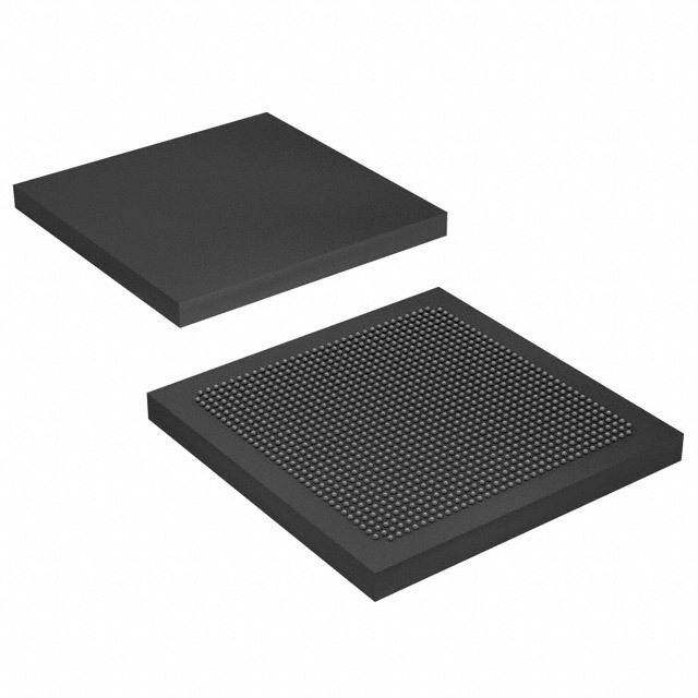
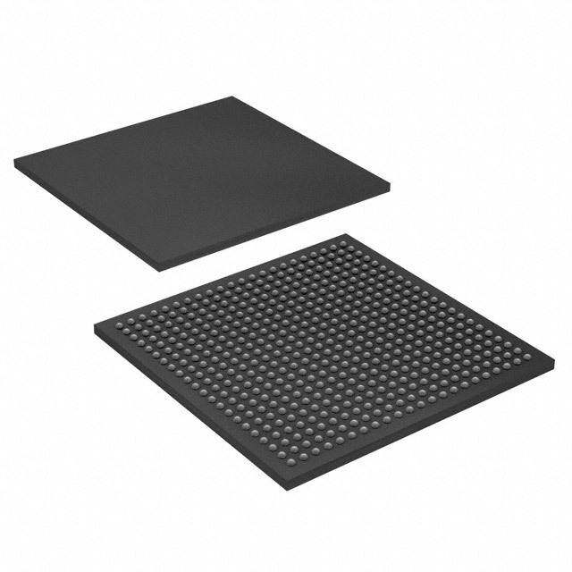
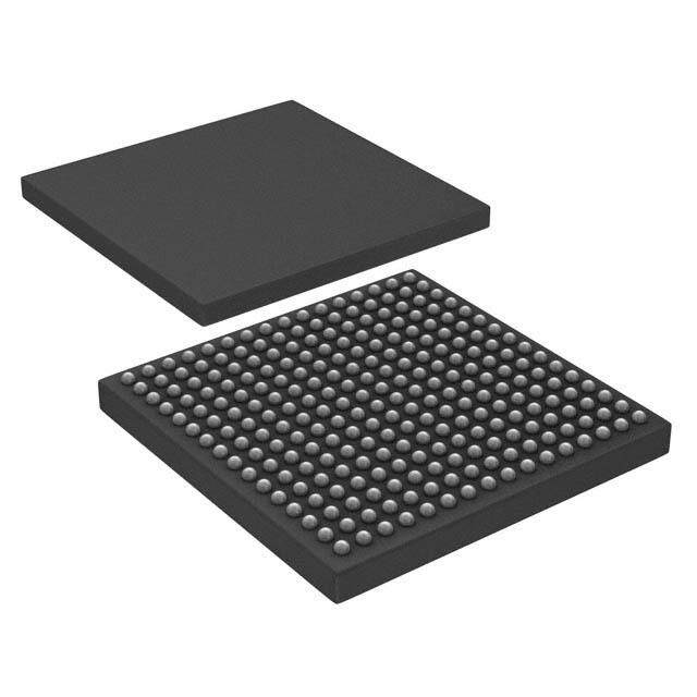
| 产品图片 |
|
| rohs | 符合RoHS无铅 / 符合限制有害物质指令(RoHS)规范要求 |
| 产品系列 | 嵌入式处理器和控制器,FPGA - 现场可编程门阵列,Altera Corporation EP4CE40U19I7NCyclone® IV E |
| 数据手册 | 点击此处下载产品Datasheet点击此处下载产品Datasheet点击此处下载产品Datasheet点击此处下载产品Datasheet |
| 产品型号 | EP4CE40U19I7N |
| 产品 | Cyclone IV E |
| 产品种类 | FPGA - 现场可编程门阵列 |
| 供应商器件封装 | 484-UBGA(19x19) |
| 其它名称 | 544-2791 |
| 商标 | Altera Corporation |
| 安装类型 | 表面贴装 |
| 安装风格 | SMD/SMT |
| 封装 | Tray |
| 封装/外壳 | 484-FBGA |
| 封装/箱体 | BGA-484 |
| 工作温度 | -40°C ~ 100°C |
| 工作电源电压 | 1 V to 1.2 V |
| 工厂包装数量 | 84 |
| 总RAM位数 | 1161216 |
| 总内存 | 1134 kbit |
| 最大工作温度 | + 85 C |
| 最大工作频率 | 200 MHz |
| 最小工作温度 | - 40 C |
| 栅极数 | - |
| 标准包装 | 84 |
| 电压-电源 | 1.15 V ~ 1.25 V |
| 系列 | Cyclone IV E |
| 输入/输出端数量 | 328 |
| 逻辑元件/单元数 | 39600 |
| 逻辑元件数量 | 39600 |
| 逻辑数组块数量——LAB | 2475 |


- 商务部:美国ITC正式对集成电路等产品启动337调查
- 曝三星4nm工艺存在良率问题 高通将骁龙8 Gen1或转产台积电
- 太阳诱电将投资9.5亿元在常州建新厂生产MLCC 预计2023年完工
- 英特尔发布欧洲新工厂建设计划 深化IDM 2.0 战略
- 台积电先进制程称霸业界 有大客户加持明年业绩稳了
- 达到5530亿美元!SIA预计今年全球半导体销售额将创下新高
- 英特尔拟将自动驾驶子公司Mobileye上市 估值或超500亿美元
- 三星加码芯片和SET,合并消费电子和移动部门,撤换高东真等 CEO
- 三星电子宣布重大人事变动 还合并消费电子和移动部门
- 海关总署:前11个月进口集成电路产品价值2.52万亿元 增长14.8%


PDF Datasheet 数据手册内容提取
1. Cyclone IV Device Datasheet March 2016 CYIV-53001-2.0 CYIV-53001-2.0 This chapter describes the electrical and switching characteristics for CycloneIV devices. Electrical characteristics include operating conditions and power consumption. Switching characteristics include transceiver specifications, core, and periphery performance. This chapter also describes I/O timing, including programmable I/O element (IOE) delay and programmable output buffer delay. This chapter includes the following sections: ■ “Operating Conditions” on page1–1 ■ “Power Consumption” on page1–16 ■ “Switching Characteristics” on page1–16 ■ “I/O Timing” on page1–37 ■ “Glossary” on page1–37 Operating Conditions When CycloneIV devices are implemented in a system, they are rated according to a set of defined parameters. To maintain the highest possible performance and reliability of CycloneIV devices, you must consider the operating requirements described in this chapter. CycloneIV devices are offered in commercial, industrial, extended industrial and, automotive grades. CycloneIVE devices offer –6(fastest), –7, –8, –8L, and –9L speed grades for commercial devices, –8L speed grades for industrial devices, and –7 speed grade for extended industrial and automotive devices. CycloneIVGX devices offer –6(fastest), –7, and –8 speed grades for commercial devices and –7 speed grade for industrial devices. f For more information about the supported speed grades for respective CycloneIV devices, refer to the CycloneIVFPGA Device Family Overview chapter. 1 CycloneIVE devices are offered in core voltages of 1.0 and 1.2V. CycloneIVE devices with a core voltage of 1.0V have an ‘L’ prefix attached to the speed grade. In this chapter, a prefix associated with the operating temperature range is attached to the speed grades; commercial with a “C” prefix, industrial with an “I” prefix, and automotive with an “A” prefix. Therefore, commercial devices are indicated as C6, C7, C8, C8L, or C9L perrespective speed grade. Industrial devices are indicated as I7, I8, or I8L. Automotive devices are indicated as A7. © 2016 Altera Corporation. All rights reserved. ALTERA, ARRIA, CYCLONE, HARDCOPY, MAX, MEGACORE, NIOS, QUARTUS and STRATIX words and logos are trademarks of Altera Corporation and registered in the U.S. Patent and Trademark Office and in other countries. All other words and logos identified as trademarks or service marks are the property of their respective holders as described at www.altera.com/common/legal.html. Altera warrants performance of its ISO semiconductor products to current specifications in accordance with Altera's standard warranty, but reserves the right to make changes to any products and 9001:2008 services at any time without notice. Altera assumes no responsibility or liability arising out of the application or use of any information, product, or service Registered described herein except as expressly agreed to in writing by Altera. Altera customers are advised to obtain the latest version of device specifications before relying on any published information and before placing orders for products or services. Cyclone IV Device Handbook, Volume 3 March 2016 Feedback Subscribe
1–2 Chapter 1: CycloneIV Device Datasheet Operating Conditions 1 CycloneIVE industrial devices I7 are offered with extended operating temperature range. Absolute Maximum Ratings Absolute maximum ratings define the maximum operating conditions for CycloneIV devices. The values are based on experiments conducted with the device and theoretical modeling of breakdown and damage mechanisms. The functional operation of the device is not implied at these conditions. Table1–1 lists the absolute maximum ratings for CycloneIV devices. c Conditions beyond those listed in Table1–1 cause permanent damage to the device. Additionally, device operation at the absolute maximum ratings for extended periods of time have adverse effects on the device. Table1–1. Absolute Maximum Ratings for CycloneIV Devices(1) Symbol Parameter Min Max Unit Core voltage, PCI Express (PCIe) hard IP V block, and transceiver physical coding sublayer –0.5 1.8 V CCINT (PCS) power supply V Phase-locked loop (PLL) analog power supply –0.5 3.75 V CCA V PLL digital power supply –0.5 1.8 V CCD_PLL V I/O banks power supply –0.5 3.75 V CCIO V Differential clock input pins power supply –0.5 4.5 V CC_CLKIN V Transceiver output buffer power supply –0.5 3.75 V CCH_GXB Transceiver physical medium attachment (PMA) V –0.5 3.75 V CCA_GXB and auxiliary power supply V Transceiver PMA and auxiliary power supply –0.5 1.8 V CCL_GXB V DC input voltage –0.5 4.2 V I I DC output current, per pin –25 40 mA OUT T Storage temperature –65 150 °C STG T Operating junction temperature –40 125 °C J Note to Table1–1: (1) Supply voltage specifications apply to voltage readings taken at the device pins with respect to ground, not at the power supply. Maximum Allowed Overshoot or Undershoot Voltage During transitions, input signals may overshoot to the voltage shown in Table1–2 and undershoot to –2.0 V for a magnitude of currents less than 100mA and for periods shorter than 20ns. Table1–2 lists the maximum allowed input overshoot voltage and the duration of the overshoot voltage as a percentage over the lifetime of the device. The maximum allowed overshoot duration is specified as a percentage of high-time over the lifetime of the device. Cyclone IV Device Handbook, March 2016 Altera Corporation Volume 3
Chapter 1: CycloneIV Device Datasheet 1–3 Operating Conditions 1 A DC signal is equivalent to 100% duty cycle. For example, a signal that overshoots to 4.3V can only be at 4.3V for 65% over the lifetime of the device; for a device lifetime of 10 years, this amounts to 65/10ths of a year. Table1–2. Maximum Allowed Overshoot During Transitions over a 10-Year Time Frame for CycloneIV Devices Symbol Parameter Condition (V) Overshoot Duration as % of High Time Unit V = 4.20 100 % I V = 4.25 98 % I V = 4.30 65 % I V = 4.35 43 % I AC Input V V = 4.40 29 % i Voltage I V = 4.45 20 % I V = 4.50 13 % I V = 4.55 9 % I V = 4.60 6 % I Figure1–1 shows the methodology to determine the overshoot duration. The overshoot voltage is shown in red and is present on the input pin of the CycloneIV device at over 4.3V but below 4.4V. From Table1–2, for an overshoot of 4.3V, the percentage of high time for the overshoot can be as high as 65% over a 10-year period. Percentage of high time is calculated as ([delta T]/T)×100. This 10-year period assumes that the device is always turned on with 100% I/O toggle rate and 50% duty cycle signal. For lower I/O toggle rates and situations in which the device is in an idle state, lifetimes are increased. Figure1–1. CycloneIV Devices Overshoot Duration 4.4 V 4.3 V 3.3 V DT T March 2016 Altera Corporation Cyclone IV Device Handbook, Volume 3
1–4 Chapter 1: CycloneIV Device Datasheet Operating Conditions Recommended Operating Conditions This section lists the functional operation limits for AC and DC parameters for CycloneIV devices. Table1–3 and Table1–4 list the steady-state voltage and current values expected from CycloneIVE and CycloneIVGX devices. All supplies must be strictly monotonic without plateaus. Table1–3. Recommended Operating Conditions for CycloneIVE Devices(1), (2) (Part 1 of 2) Symbol Parameter Conditions Min Typ Max Unit Supply voltage for internal logic, — 1.15 1.2 1.25 V 1.2-V operation V (3) CCINT Supply voltage for internal logic, — 0.97 1.0 1.03 V 1.0-V operation Supply voltage for output buffers, — 3.135 3.3 3.465 V 3.3-V operation Supply voltage for output buffers, — 2.85 3 3.15 V 3.0-V operation Supply voltage for output buffers, — 2.375 2.5 2.625 V 2.5-V operation V (3), (4) CCIO Supply voltage for output buffers, — 1.71 1.8 1.89 V 1.8-V operation Supply voltage for output buffers, — 1.425 1.5 1.575 V 1.5-V operation Supply voltage for output buffers, — 1.14 1.2 1.26 V 1.2-V operation Supply (analog) voltage for PLL V (3) — 2.375 2.5 2.625 V CCA regulator Supply (digital) voltage for PLL, — 1.15 1.2 1.25 V 1.2-V operation V (3) CCD_PLL Supply (digital) voltage for PLL, — 0.97 1.0 1.03 V 1.0-V operation V Input voltage — –0.5 — 3.6 V I V Output voltage — 0 — V V O CCIO For commercial use 0 — 85 °C For industrial use –40 — 100 °C T Operating junction temperature J For extended temperature –40 — 125 °C For automotive use –40 — 125 °C Standard power-on reset 50µs — 50ms — t Power supply ramp time (POR) (5) RAMP Fast POR (6) 50µs — 3ms — Cyclone IV Device Handbook, March 2016 Altera Corporation Volume 3
Chapter 1: CycloneIV Device Datasheet 1–5 Operating Conditions Table1–3. Recommended Operating Conditions for CycloneIVE Devices(1), (2) (Part 2 of 2) Symbol Parameter Conditions Min Typ Max Unit Magnitude of DC current across I — — — 10 mA Diode PCI-clamp diode when enable Notes to Table1–3: (1) CycloneIVE 1.0V core voltage devices only support C8L, C9L, and I8L speed grades. CycloneIVE 1.2V core voltage devices only support C6, C7, C8, I7, and A7 speed grades. (2) V for all I/O banks must be powered up during device operation. All VCCA pins must be powered to 2.5V (even when PLLs are not used) CCIO and must be powered up and powered down at the same time. (3) V must rise monotonically. CC (4) V powers all input buffers. CCIO (5) The POR time for Standard POR ranges between 50 and 200ms. Each individual power supply must reach the recommended operating range within 50ms. (6) The POR time for Fast POR ranges between 3 and 9ms. Each individual power supply must reach the recommended operating range within 3ms. Table1–4. Recommended Operating Conditions for CycloneIVGX Devices (Part 1 of 2) Symbol Parameter Conditions Min Typ Max Unit Core voltage, PCIe hard IP block, and V (3) — 1.16 1.2 1.24 V CCINT transceiver PCS power supply V (1),(3) PLL analog power supply — 2.375 2.5 2.625 V CCA V (2) PLL digital power supply — 1.16 1.2 1.24 V CCD_PLL I/O banks power supply for 3.3-V — 3.135 3.3 3.465 V operation I/O banks power supply for 3.0-V — 2.85 3 3.15 V operation I/O banks power supply for 2.5-V — 2.375 2.5 2.625 V operation V (3),(4) CCIO I/O banks power supply for 1.8-V — 1.71 1.8 1.89 V operation I/O banks power supply for 1.5-V — 1.425 1.5 1.575 V operation I/O banks power supply for 1.2-V — 1.14 1.2 1.26 V operation Differential clock input pins power — 3.135 3.3 3.465 V supply for 3.3-V operation Differential clock input pins power — 2.85 3 3.15 V supply for 3.0-V operation Differential clock input pins power — 2.375 2.5 2.625 V V supply for 2.5-V operation CC_CLKIN (3),(5),(6) Differential clock input pins power — 1.71 1.8 1.89 V supply for 1.8-V operation Differential clock input pins power — 1.425 1.5 1.575 V supply for 1.5-V operation Differential clock input pins power — 1.14 1.2 1.26 V supply for 1.2-V operation V Transceiver output buffer power supply — 2.375 2.5 2.625 V CCH_GXB March 2016 Altera Corporation Cyclone IV Device Handbook, Volume 3
1–6 Chapter 1: CycloneIV Device Datasheet Operating Conditions Table1–4. Recommended Operating Conditions for CycloneIVGX Devices (Part 2 of 2) Symbol Parameter Conditions Min Typ Max Unit Transceiver PMA and auxiliary power V — 2.375 2.5 2.625 V CCA_GXB supply Transceiver PMA and auxiliary power V — 1.16 1.2 1.24 V CCL_GXB supply V DC input voltage — –0.5 — 3.6 V I V DC output voltage — 0 — V V O CCIO For commercial use 0 — 85 °C T Operating junction temperature J For industrial use –40 — 100 °C Standard power-on reset 50 µs — 50 ms — t Power supply ramp time (POR) (7) RAMP Fast POR (8) 50 µs — 3 ms — Magnitude of DC current across I — — — 10 mA Diode PCI-clamp diode when enabled Notes to Table1–4: (1) All VCCA pins must be powered to 2.5 V (even when PLLs are not used) and must be powered up and powered down at the same time. (2) You must connect V to V through a decoupling capacitor and ferrite bead. CCD_PLL CCINT (3) Power supplies must rise monotonically. (4) V for all I/O banks must be powered up during device operation. Configurations pins are powered up by V of I/O Banks 3, 8, and 9 where CCIO CCIO I/O Banks 3 and 9 only support V of 1.5, 1.8, 2.5, 3.0, and 3.3V. For fast passive parallel (FPP) configuration mode, the V level of I/O CCIO CCIO Bank8 must be powered up to 1.5, 1.8, 2.5, 3.0, and 3.3 V. (5) You must set V to 2.5 V if you use CLKIN as a high-speed serial interface (HSSI) refclk or as a DIFFCLK input. CC_CLKIN (6) The CLKIN pins in I/O Banks 3B and 8B can support single-ended I/O standard when the pins are used to clock left PLLs in non-transceiver applications. (7) The POR time for Standard POR ranges between 50 and 200ms. V , V , and V of I/O Banks 3, 8, and 9 must reach the recommended CCINT CCA CCIO operating range within 50 ms. (8) The POR time for Fast POR ranges between 3 and 9ms. V , V , and V of I/O Banks 3, 8, and 9 must reach the recommended operating CCINT CCA CCIO range within 3 ms. ESD Performance This section lists the electrostatic discharge (ESD) voltages using the human body model (HBM) and charged device model (CDM) for CycloneIV devices general purpose I/Os (GPIOs) and high-speed serial interface (HSSI) I/Os. Table1–5 lists the ESD for CycloneIV devices GPIOs and HSSI I/Os. Table1–5. ESD for Cyclone IV Devices GPIOs and HSSI I/Os Symbol Parameter Passing Voltage Unit ESD voltage using the HBM (GPIOs)(1) ± 2000 V V ESDHBM ESD using the HBM (HSSI I/Os) (2) ± 1000 V ESD using the CDM (GPIOs) ± 500 V V ESDCDM ESD using the CDM (HSSI I/Os) (2) ± 250 V Notes to Table1–5: (1) The passing voltage for EP4CGX15 and EP4CGX30 row I/Os is ±1000V. (2) This value is applicable only to Cyclone IV GX devices. Cyclone IV Device Handbook, March 2016 Altera Corporation Volume 3
Chapter 1: CycloneIV Device Datasheet 1–7 Operating Conditions DC Characteristics This section lists the I/O leakage current, pin capacitance, on-chip termination (OCT) tolerance, and bus hold specifications for CycloneIV devices. Supply Current The device supply current requirement is the minimum current drawn from the power supply pins that can be used as a reference for power size planning. Use the Excel-based early power estimator (EPE) to get the supply current estimates for your design because these currents vary greatly with the resources used. Table1–6 lists the I/O pin leakage current for CycloneIV devices. Table1–6. I/O Pin Leakage Current for CycloneIV Devices(1), (2) Symbol Parameter Conditions Device Min Typ Max Unit I Input pin leakage current V = 0V to V — –10 — 10 A I I CCIOMAX Tristated I/O pin leakage I V = 0V to V — –10 — 10 A OZ current O CCIOMAX Notes to Table1–6: (1) This value is specified for normal device operation. The value varies during device power-up. This applies for all V settings (3.3, 3.0, 2.5, CCIO 1.8, 1.5, and 1.2 V). (2) The 10 A I/O leakage current limit is applicable when the internal clamping diode is off. A higher current can be observed when the diode is on. Bus Hold The bus hold retains the last valid logic state after the source driving it either enters the high impedance state or is removed. Each I/O pin has an option to enable bus hold in user mode. Bus hold is always disabled in configuration mode. Table1–7 lists bus hold specifications for CycloneIV devices. Table1–7. Bus Hold Parameter for CycloneIV Devices (Part 1 of 2)(1) V (V) CCIO Parameter Condition 1.2 1.5 1.8 2.5 3.0 3.3 Unit Min Max Min Max Min Max Min Max Min Max Min Max Bus hold low, V > V IN IL 8 — 12 — 30 — 50 — 70 — 70 — A sustaining (maximum) current Bus hold high, V < V IN IL –8 — –12 — –30 — –50 — –70 — –70 — A sustaining (minimum) current Bus hold low, 0 V < V < V — 125 — 175 — 200 — 300 — 500 — 500 A overdrive IN CCIO current Bus hold high, 0 V < V < V — –125 — –175 — –200 — –300 — –500 — –500 A overdrive IN CCIO current March 2016 Altera Corporation Cyclone IV Device Handbook, Volume 3
1–8 Chapter 1: CycloneIV Device Datasheet Operating Conditions Table1–7. Bus Hold Parameter for CycloneIV Devices (Part 2 of 2)(1) V (V) CCIO Parameter Condition 1.2 1.5 1.8 2.5 3.0 3.3 Unit Min Max Min Max Min Max Min Max Min Max Min Max Bus hold trip — 0.3 0.9 0.375 1.125 0.68 1.07 0.7 1.7 0.8 2 0.8 2 V point Note to Table1–7: (1) Bus hold trip points are based on the calculated input voltages from the JEDEC standard. OCT Specifications Table1–8 lists the variation of OCT without calibration across process, temperature, and voltage (PVT). Table1–8. Series OCT Without Calibration Specifications for CycloneIV Devices Resistance Tolerance Description V (V) Industrial, Extended Unit CCIO Commercial Maximum industrial, and Automotive Maximum 3.0 ±30 ±40 % 2.5 ±30 ±40 % Series OCT without 1.8 ±40 ±50 % calibration 1.5 ±50 ±50 % 1.2 ±50 ±50 % OCT calibration is automatically performed at device power-up for OCT-enabled I/Os. Table1–9 lists the OCT calibration accuracy at device power-up. Table1–9. Series OCT with Calibration at Device Power-Up Specifications for CycloneIV Devices Calibration Accuracy Description V (V) Industrial, Extended Unit CCIO Commercial Maximum industrial, and Automotive Maximum 3.0 ±10 ±10 % 2.5 ±10 ±10 % Series OCT with calibration at device 1.8 ±10 ±10 % power-up 1.5 ±10 ±10 % 1.2 ±10 ±10 % Cyclone IV Device Handbook, March 2016 Altera Corporation Volume 3
Chapter 1: CycloneIV Device Datasheet 1–9 Operating Conditions The OCT resistance may vary with the variation of temperature and voltage after calibration at device power-up. Use Table1–10 and Equation1–1 to determine the final OCT resistance considering the variations after calibration at device power-up. Table1–10 lists the change percentage of the OCT resistance with voltage and temperature. Table1–10. OCT Variation After Calibration at Device Power-Up for CycloneIV Devices Nominal Voltage dR/dT (%/°C) dR/dV (%/mV) 3.0 0.262 –0.026 2.5 0.234 –0.039 1.8 0.219 –0.086 1.5 0.199 –0.136 1.2 0.161 –0.288 Equation1–1. Final OCT Resistance(1), (2), (3), (4), (5), (6) R = (V – V ) × 1000 × dR/dV ––––– (7) V 2 1 R = (T – T ) × dR/dT ––––– (8) T 2 1 For R < 0; MF = 1/ (|R|/100 + 1) ––––– (9) x x x For R > 0; MF = R/100 + 1 ––––– (10) x x x MF = MF × MF ––––– (11) V T R = R × MF ––––– (12) final initial Notes to Equation1–1: (1) T is the final temperature. 2 (2) T is the initial temperature. 1 (3) MF is multiplication factor. (4) R is final resistance. final (5) R is initial resistance. initial (6) Subscript refers to both and . x V T (7) R is a variation of resistance with voltage. V (8) R is a variation of resistance with temperature. T (9) dR/dT is the change percentage of resistance with temperature after calibration at device power-up. (10)dR/dV is the change percentage of resistance with voltage after calibration at device power-up. (11)V is final voltage. 2 (12)V is the initial voltage. 1 March 2016 Altera Corporation Cyclone IV Device Handbook, Volume 3
1–10 Chapter 1: CycloneIV Device Datasheet Operating Conditions Example1–1 shows how to calculate the change of 50-I/O impedance from 25°C at 3.0 V to 85°C at 3.15 V. Example1–1. Impedance Change R = (3.15 – 3) × 1000 × –0.026 = –3.83 V R = (85 – 25) × 0.262 = 15.72 T Because R is negative, V MF = 1 / (3.83/100 + 1) = 0.963 V Because R is positive, T MF = 15.72/100 + 1 = 1.157 T MF = 0.963 × 1.157 = 1.114 R = 50 × 1.114 = 55.71 final Pin Capacitance Table1–11 lists the pin capacitance for CycloneIV devices. Table1–11. Pin Capacitance for CycloneIV Devices (1) Typical – Typical – Typical – Quad Flat Quad Flat Ball-Grid Symbol Parameter Unit Pack No Leads Array (QFP) (QFN) (BGA) C Input capacitance on top and bottom I/O pins 7 7 6 pF IOTB C Input capacitance on right I/O pins 7 7 5 pF IOLR C Input capacitance on right I/O pins with dedicated LVDS output 8 8 7 pF LVDSLR C Input capacitance on right dual-purpose VREF pin when used as VREFLR 21 21 21 pF (2) V or user I/O pin REF C Input capacitance on top and bottom dual-purpose VREF pin when VREFTB 23 (3) 23 23 pF (2) used as V or user I/O pin REF C Input capacitance on top and bottom dedicated clock input pins 7 7 6 pF CLKTB C Input capacitance on right dedicated clock input pins 6 6 5 pF CLKLR Notes to Table1–11: (1) The pin capacitance applies to FBGA, UBGA, and MBGA packages. (2) When you use the VREF pin as a regular input or output, you can expect a reduced performance of toggle rate and t because of higher pin CO capacitance. (3) C for the EP4CE22 device is 30pF. VREFTB Cyclone IV Device Handbook, March 2016 Altera Corporation Volume 3
Chapter 1: CycloneIV Device Datasheet 1–11 Operating Conditions Internal Weak Pull-Up and Weak Pull-Down Resistor Table1–12 lists the weak pull-up and pull-down resistor values for CycloneIV devices. Table1–12. Internal Weak Pull-Up and Weak Pull-Down Resistor Values for CycloneIV Devices(1) Symbol Parameter Conditions Min Typ Max Unit V = 3.3 V ± 5% (2), (3) 7 25 41 k CCIO V = 3.0 V ± 5% (2), (3) 7 28 47 k Value of the I/O pin pull-up resistor CCIO before and during configuration, as VCCIO = 2.5 V ± 5% (2), (3) 8 35 61 k R _PU well as user mode if you enable the V = 1.8 V ± 5% (2), (3) 10 57 108 k CCIO programmable pull-up resistor option V = 1.5 V ± 5% (2), (3) 13 82 163 k CCIO V = 1.2 V ± 5% (2), (3) 19 143 351 k CCIO V = 3.3 V ± 5% (4) 6 19 30 k CCIO V = 3.0 V ± 5% (4) 6 22 36 k CCIO Value of the I/O pin pull-down resistor R V = 2.5 V ± 5% (4) 6 25 43 k _PD before and during configuration CCIO V = 1.8 V ± 5% (4) 7 35 71 k CCIO V = 1.5 V ± 5% (4) 8 50 112 k CCIO Notes to Table1–12: (1) All I/O pins have an option to enable weak pull-up except the configuration, test, and JTAG pins. The weak pull-down feature is only available for JTAG TCK. (2) Pin pull-up resistance values may be lower if an external source drives the pin higher than V . CCIO (3) R = (V –V)/I _PU CCIO I R_PU Minimum condition: –40°C; V = V + 5%, V = V + 5% – 50mV; CCIO CC I CC Typical condition: 25°C; V = V , V = 0V; CCIO CC I Maximum condition: 100°C; V = V – 5%, V = 0V; in which V refers to the input voltage at the I/O pin. CCIO CC I I (4) R = V/I _PD I R_PD Minimum condition: –40°C; V = V + 5%, V = 50mV; CCIO CC I Typical condition: 25°C; V = V , V = V –5%; CCIO CC I CC Maximum condition: 100°C; V = V – 5%, V = V –5%; in which V refers to the input voltage at the I/O pin. CCIO CC I CC I Hot-Socketing Table1–13 lists the hot-socketing specifications for CycloneIV devices. Table1–13. Hot-Socketing Specifications for CycloneIV Devices Symbol Parameter Maximum I DC current per I/O pin 300 A IOPIN(DC) I AC current per I/O pin 8mA (1) IOPIN(AC) I DC current per transceiver TX pin 100mA XCVRTX(DC) I DC current per transceiver RX pin 50mA XCVRRX(DC) Note to Table1–13: (1) The I/O ramp rate is 10 ns or more. For ramp rates faster than 10 ns, |IIOPIN|=C dv/dt, in which C is the I/O pin capacitance and dv/dt is the slew rate. 1 During hot-socketing, the I/O pin capacitance is less than 15 pF and the clock pin capacitance is less than 20 pF. March 2016 Altera Corporation Cyclone IV Device Handbook, Volume 3
1–12 Chapter 1: CycloneIV Device Datasheet Operating Conditions Schmitt Trigger Input CycloneIV devices support Schmitt trigger input on the TDI, TMS, TCK, nSTATUS, nCONFIG, nCE, CONF_DONE, and DCLK pins. A Schmitt trigger feature introduces hysteresis to the input signal for improved noise immunity, especially for signals with slow edge rate. Table1–14 lists the hysteresis specifications across the supported V range for Schmitt trigger inputs in CycloneIV devices. CCIO Table1–14. Hysteresis Specifications for Schmitt Trigger Input in CycloneIV Devices Symbol Parameter Conditions (V) Minimum Unit V =3.3 200 mV CCIO Hysteresis for Schmitt trigger VCCIO=2.5 200 mV V SCHMITT input V =1.8 140 mV CCIO V =1.5 110 mV CCIO I/O Standard Specifications The following tables list input voltage sensitivities (V and V ), output voltage (V IH IL OH and V ), and current drive characteristics (I and I ), for various I/O standards OL OH OL supported by CycloneIV devices. Table1–15 through Table1–20 provide the I/O standard specifications for CycloneIV devices. Table1–15. Single-Ended I/O Standard Specifications for CycloneIV Devices(1), (2) V (V) V (V) V (V) V (V) V (V) I I CCIO IL IH OL OH OL OH I/O Standard (mA) (mA) Min Typ Max Min Max Min Max Max Min (4) (4) 3.3-V LVTTL (3) 3.135 3.3 3.465 — 0.8 1.7 3.6 0.45 2.4 4 –4 3.3-V LVCMOS (3) 3.135 3.3 3.465 — 0.8 1.7 3.6 0.2 V – 0.2 2 –2 CCIO 3.0-V LVTTL (3) 2.85 3.0 3.15 –0.3 0.8 1.7 V + 0.3 0.45 2.4 4 –4 CCIO 3.0-V LVCMOS (3) 2.85 3.0 3.15 –0.3 0.8 1.7 V + 0.3 0.2 V – 0.2 0.1 –0.1 CCIO CCIO 2.5V (3) 2.375 2.5 2.625 –0.3 0.7 1.7 V + 0.3 0.4 2.0 1 –1 CCIO 0.35 x 0.65 x V – 1.8V 1.71 1.8 1.89 –0.3 2.25 0.45 CCIO 2 –2 V V 0.45 CCIO CCIO 0.35 x 0.65 x 0.25 x 0.75 x 1.5V 1.425 1.5 1.575 –0.3 V + 0.3 2 –2 V V CCIO V V CCIO CCIO CCIO CCIO 0.35 x 0.65 x 0.25 x 0.75 x 1.2V 1.14 1.2 1.26 –0.3 V + 0.3 2 –2 V V CCIO V V CCIO CCIO CCIO CCIO 0.3 x 0.5 x 3.0-V PCI 2.85 3.0 3.15 — V + 0.3 0.1 x V 0.9 x V 1.5 –0.5 V V CCIO CCIO CCIO CCIO CCIO 0.35 x 0.5 x 3.0-V PCI-X 2.85 3.0 3.15 — V + 0.3 0.1 x V 0.9 x V 1.5 –0.5 V V CCIO CCIO CCIO CCIO CCIO Notes to Table1–15: (1) For voltage-referenced receiver input waveform and explanation of terms used in Table1–15, refer to “Glossary” on page1–37. (2) AC load CL = 10 pF (3) For more information about interfacing CycloneIV devices with 3.3/3.0/2.5-V LVTTL/LVCMOS I/O standards, refer to AN447: Interfacing CycloneIII and CycloneIV Devices with 3.3/3.0/2.5-V LVTTL/LVCMOS I/O Systems. (4) To meet the IOL and IOH specifications, you must set the current strength settings accordingly. For example, to meet the 3.3-V LVTTL specification (4 mA), set the current strength settings to 4 mA or higher. Setting at lower current strength may not meet the IOL and IOH specifications in the handbook. Cyclone IV Device Handbook, March 2016 Altera Corporation Volume 3
Chapter 1: CycloneIV Device Datasheet 1–13 Operating Conditions Table1–16. Single-Ended SSTL and HSTL I/O Reference Voltage Specifications for CycloneIV Devices(1) V (V) V (V) V (V) (2) I/O CCIO REF TT Standard Min Typ Max Min Typ Max Min Typ Max SSTL-2 V – V + 2.375 2.5 2.625 1.19 1.25 1.31 REF V REF Class I, II 0.04 REF 0.04 SSTL-18 V – V + 1.7 1.8 1.9 0.833 0.9 0.969 REF V REF Class I, II 0.04 REF 0.04 HSTL-18 1.71 1.8 1.89 0.85 0.9 0.95 0.85 0.9 0.95 Class I, II HSTL-15 1.425 1.5 1.575 0.71 0.75 0.79 0.71 0.75 0.79 Class I, II HSTL-12 0.48 x VCCIO (3) 0.5 x VCCIO (3) 0.52 x VCCIO (3) 0.5 x 1.14 1.2 1.26 — — Class I, II 0.47 x VCCIO (4) 0.5 x VCCIO (4) 0.53 x VCCIO (4) VCCIO Notes to Table1–16: (1) For an explanation of terms used in Table1–16, refer to “Glossary” on page1–37. (2) V of the transmitting device must track V of the receiving device. TT REF (3) Value shown refers to DC input reference voltage, V . REF(DC) (4) Value shown refers to AC input reference voltage, V . REF(AC) Table1–17. Single-Ended SSTL and HSTL I/O Standards Signal Specifications for CycloneIV Devices V (V) V (V) V (V) V (V) V (V) V (V) I/O IL(DC) IH(DC) IL(AC) IH(AC) OL OH I I OL OH Standard (mA) (mA) Min Max Min Max Min Max Min Max Max Min SSTL-2 V – V + V – V + V – V + — REF REF — — REF REF — TT TT 8.1 –8.1 Class I 0.18 0.18 0.35 0.35 0.57 0.57 SSTL-2 V – V + V – V + V – V + — REF REF — — REF REF — TT TT 16.4 –16.4 Class II 0.18 0.18 0.35 0.35 0.76 0.76 SSTL-18 V – V + V – V + V – V + — REF REF — — REF REF — TT TT 6.7 –6.7 Class I 0.125 0.125 0.25 0.25 0.475 0.475 SSTL-18 V – V + V – V + V – — REF REF — — REF REF — 0.28 CCIO 13.4 –13.4 Class II 0.125 0.125 0.25 0.25 0.28 HSTL-18 V – V + V – V + V – — REF REF — — REF REF — 0.4 CCIO 8 –8 Class I 0.1 0.1 0.2 0.2 0.4 HSTL-18 V – V + V – V + V – — REF REF — — REF REF — 0.4 CCIO 16 –16 Class II 0.1 0.1 0.2 0.2 0.4 HSTL-15 V – V + V – V + V – — REF REF — — REF REF — 0.4 CCIO 8 –8 Class I 0.1 0.1 0.2 0.2 0.4 HSTL-15 V – V + V – V + V – — REF REF — — REF REF — 0.4 CCIO 16 –16 Class II 0.1 0.1 0.2 0.2 0.4 HSTL-12 V – V + V – V + V + 0.25 × 0.75 × –0.15 REF REF V + 0.15 –0.24 REF REF CCIO 8 –8 Class I 0.08 0.08 CCIO 0.15 0.15 0.24 V V CCIO CCIO HSTL-12 V – V + V – V + V + 0.25 × 0.75 × –0.15 REF REF V + 0.15 –0.24 REF REF CCIO 14 –14 Class II 0.08 0.08 CCIO 0.15 0.15 0.24 V V CCIO CCIO March 2016 Altera Corporation Cyclone IV Device Handbook, Volume 3
1–14 Chapter 1: CycloneIV Device Datasheet Operating Conditions f For more information about receiver input and transmitter output waveforms, and for other differential I/O standards, refer to the I/O Features in CycloneIV Devices chapter. Table1–18. Differential SSTL I/O Standard Specifications for CycloneIV Devices(1) V V (V) V (V) V (V) Swing(AC) V (V) CCIO Swing(DC) X(AC) (V) OX(AC) I/O Standard Min Typ Max Min Max Min Typ Max Min Max Min Typ Max SSTL-2 V /2 V V /2 – V /2 2.375 2.5 2.625 0.36 V V /2 – 0.2 — CCIO 0.7 CCI CCIO — CCIO Class I, II CCIO CCIO + 0.2 0.125 + 0.125 O SSTL-18 V /2 – V /2 V V /2 – V /2 1.7 1.8 1.90 0.25 V CCIO — CCIO 0.5 CCI CCIO — CCIO Class I, II CCIO 0.175 + 0.175 0.125 + 0.125 O Note to Table1–18: (1) Differential SSTL requires a V input. REF Table1–19. Differential HSTL I/O Standard Specifications for CycloneIV Devices(1) V (V) V (V) V (V) V (V) V (V) CCIO DIF(DC) X(AC) CM(DC) DIF(AC) I/O Standard Mi Min Typ Max Min Max Min Typ Max Min Typ Max Max n HSTL-18 1.71 1.8 1.89 0.2 — 0.85 — 0.95 0.85 — 0.95 0.4 — Class I, II HSTL-15 1.425 1.5 1.575 0.2 — 0.71 — 0.79 0.71 — 0.79 0.4 — Class I, II HSTL-12 0.52 x 0.48 x 0.52 x 0.48 x 1.14 1.2 1.26 0.16 V 0.48 x V — — 0.3 Class I, II CCIO CCIO V V V V CCIO CCIO CCIO CCIO Note to Table1–19: (1) Differential HSTL requires a V input. REF Table1–20. Differential I/O Standard Specifications for CycloneIV Devices (1) (Part 1 of 2) V (V) V (mV) V (V) (2) V (mV) (3) V (V) (3) CCIO ID IcM OD OS I/O Standard Min Typ Max Min Max Min Condition Max Min Typ Max Min Typ Max 0.05 D 500 Mbps 1.80 MAX LVPECL 500 Mbps D (Row I/Os) 2.375 2.5 2.625 100 — 0.55 MAX 1.80 — — — — — — 700 Mbps (6) 1.05 D > 700 Mbps 1.55 MAX 0.05 D 500Mbps 1.80 MAX LVPECL 500Mbps D (Column 2.375 2.5 2.625 100 — 0.55 MAX 1.80 — — — — — — 700Mbps I/Os) (6) 1.05 D > 700Mbps 1.55 MAX 0.05 D 500Mbps 1.80 MAX LVDS (Row 500Mbps D 2.375 2.5 2.625 100 — 0.55 MAX 1.80 247 — 600 1.125 1.25 1.375 I/Os) 700Mbps 1.05 D > 700Mbps 1.55 MAX Cyclone IV Device Handbook, March 2016 Altera Corporation Volume 3
Chapter 1: CycloneIV Device Datasheet 1–15 Operating Conditions Table1–20. Differential I/O Standard Specifications for CycloneIV Devices (1) (Part 2 of 2) V (V) V (mV) V (V) (2) V (mV) (3) V (V) (3) CCIO ID IcM OD OS I/O Standard Min Typ Max Min Max Min Condition Max Min Typ Max Min Typ Max 0.05 D 500Mbps 1.80 MAX LVDS 500Mbps D (Column 2.375 2.5 2.625 100 — 0.55 MAX 1.80 247 — 600 1.125 1.25 1.375 700Mbps I/Os) 1.05 D > 700Mbps 1.55 MAX BLVDS (Row 2.375 2.5 2.625 100 — — — — — — — — — — I/Os) (4) BLVDS (Column 2.375 2.5 2.625 100 — — — — — — — — — — I/Os) (4) mini-LVDS (Row I/Os) 2.375 2.5 2.625 — — — — — 300 — 600 1.0 1.2 1.4 (5) mini-LVDS (Column 2.375 2.5 2.625 — — — — — 300 — 600 1.0 1.2 1.4 I/Os) (5) RSDS® (Row 2.375 2.5 2.625 — — — — — 100 200 600 0.5 1.2 1.5 I/Os)(5) RSDS (Column 2.375 2.5 2.625 — — — — — 100 200 600 0.5 1.2 1.5 I/Os) (5) PPDS (Row 2.375 2.5 2.625 — — — — — 100 200 600 0.5 1.2 1.4 I/Os) (5) PPDS (Column 2.375 2.5 2.625 — — — — — 100 200 600 0.5 1.2 1.4 I/Os) (5) Notes to Table1–20: (1) For an explanation of terms used in Table1–20, refer to “Glossary” on page1–37. (2) V range: 0V V 1.85V. IN IN (3) R range: 90 R 110 . L L (4) There are no fixed V , V , and V specifications for BLVDS. They depend on the system topology. IN OD OS (5) The Mini-LVDS, RSDS, and PPDS standards are only supported at the output pins. (6) The LVPECL I/O standard is only supported on dedicated clock input pins. This I/O standard is not supported for output pins. March 2016 Altera Corporation Cyclone IV Device Handbook, Volume 3
1–16 Chapter 1: CycloneIV Device Datasheet Power Consumption Power Consumption Use the following methods to estimate power for a design: ■ the Excel-based EPE ■ the QuartusII PowerPlay power analyzer feature The interactive Excel-based EPE is used prior to designing the device to get a magnitude estimate of the device power. The QuartusII PowerPlay power analyzer provides better quality estimates based on the specifics of the design after place-and-route is complete. The PowerPlay power analyzer can apply a combination of user-entered, simulation-derived, and estimated signal activities that, combined with detailed circuit models, can yield very accurate power estimates. f For more information about power estimation tools, refer to the Early Power Estimator User Guide and the PowerPlay Power Analysis chapter in volume 3 of the QuartusII Handbook. Switching Characteristics This section provides performance characteristics of CycloneIV core and periphery blocks for commercial grade devices. These characteristics can be designated as Preliminary or Final. ■ Preliminary characteristics are created using simulation results, process data, and other known parameters. The upper-right hand corner of these tables show the designation as “Preliminary”. ■ Final numbers are based on actual silicon characterization and testing. The numbers reflect the actual performance of the device under worst-case silicon process, voltage, and junction temperature conditions. There are no designations on finalized tables. Cyclone IV Device Handbook, March 2016 Altera Corporation Volume 3
Chapter 1: CycloneIV Device Datasheet 1–17 Switching Characteristics Transceiver Performance Specifications Table1–21 lists the CycloneIV GX transceiver specifications. Table1–21. Transceiver Specification for CycloneIV GX Devices (Part 1 of 4) C6 C7, I7 C8 Symbol/ Conditions Unit Description Min Typ Max Min Typ Max Min Typ Max Reference Clock Supported I/O 1.2V PCML, 1.5V PCML, 3.3V PCML, Differential LVPECL, LVDS, HCSL Standards Input frequency from REFCLK input — 50 — 156.25 50 — 156.25 50 — 156.25 MHz pins Spread-spectrum Physical interface modulating clock for PCI Express 30 — 33 30 — 33 30 — 33 kHz frequency (PIPE) mode Spread-spectrum 0 to 0 to 0 to PIPE mode — — — — — — — downspread –0.5% –0.5% –0.5% Peak-to-peak differential input — 0.1 — 1.6 0.1 — 1.6 0.1 — 1.6 V voltage V (AC coupled) — 1100 ± 5% 1100 ± 5% 1100 ± 5% mV ICM HCSL I/O V (DC coupled) standard for PCIe 250 — 550 250 — 550 250 — 550 mV ICM reference clock Transmitter REFCLK — — –123 — — –123 — — –123 dBc/Hz Phase Noise(1) Frequency offset Transmitter REFCLK = 1MHz – 8MHZ — — 42.3 — — 42.3 — — 42.3 ps Total Jitter(1) 2000 2000 2000 R — — — — — — — ref ± 1% ± 1% ± 1% Transceiver Clock cal_blk_clk clock — 10 — 125 10 — 125 10 — 125 MHz frequency fixedclk clock PCIe Receiver — 125 — — 125 — — 125 — MHz frequency Detect Dynamic 2.5/ 2.5/ 2.5/ reconfig_clk reconfiguration 37.5 — 50 37.5 — 50 37.5 — 50 MHz clock frequency clock frequency (2) (2) (2) Delta time between — — — 2 — — 2 — — 2 ms reconfig_clk Transceiver block minimum — — 1 — — 1 — — 1 — µs power-down pulse width March 2016 Altera Corporation Cyclone IV Device Handbook, Volume 3
1–18 Chapter 1: CycloneIV Device Datasheet Switching Characteristics Table1–21. Transceiver Specification for CycloneIV GX Devices (Part 2 of 4) C6 C7, I7 C8 Symbol/ Conditions Unit Description Min Typ Max Min Typ Max Min Typ Max Receiver 1.4V PCML, Supported I/O 1.5V PCML, Standards 2.5V PCML, LVPECL, LVDS Data rate (F324 and — 600 — 2500 600 — 2500 600 — 2500 Mbps smaller package)(15) Data rate (F484 and — 600 — 3125 600 — 3125 600 — 2500 Mbps larger package)(15) Absolute V for a MAX — — — 1.6 — — 1.6 — — 1.6 V receiver pin (3) Operational V for MAX — — — 1.5 — — 1.5 — — 1.5 V a receiver pin Absolute V for a MIN — –0.4 — — –0.4 — — –0.4 — — V receiver pin V = 0.82V Peak-to-peak ICM setting, Data Rate differential input 0.1 — 2.7 0.1 — 2.7 0.1 — 2.7 V = 600Mbps to voltage V (diff p-p) ID 3.125Gbps V = 0.82V 820 ± 820 ± 820 ± V ICM — — — — — — mV ICM setting 10% 10% 10% Differential on-chip 100 setting — 100 — — 100 — — 100 — termination resistors 150 setting — 150 — — 150 — — 150 — PIPE, Serial Differential and Rapid I/O SR, common mode Compliant — SATA, CPRI LV, return loss SDI, XAUI Programmable ppm ± 62.5, 100, 125, 200, — ppm detector (4) 250, 300 Clock data recovery ±300 ±300 (CDR) ppm ±300 (5), (5), (5), tolerance (without — — — ±350 — — — — ppm ±350 ±350 spread-spectrum (6),(7) (6),(7) (6),(7) clocking enabled) CDR ppm tolerance 350 to 350 to 350 to (with synchronous — — — –5350 — — –5350 — — –5350 ppm spread-spectrum (7),(9) (7),(9) (7),(9) clocking enabled)(8) Run length — — 80 — — 80 — — 80 — UI No Equalization — — 1.5 — — 1.5 — — 1.5 dB Programmable Medium Low — — 4.5 — — 4.5 — — 4.5 dB equalization Medium High — — 5.5 — — 5.5 — — 5.5 dB High — — 7 — — 7 — — 7 dB Cyclone IV Device Handbook, March 2016 Altera Corporation Volume 3
Chapter 1: CycloneIV Device Datasheet 1–19 Switching Characteristics Table1–21. Transceiver Specification for CycloneIV GX Devices (Part 3 of 4) C6 C7, I7 C8 Symbol/ Conditions Unit Description Min Typ Max Min Typ Max Min Typ Max Signal detect/loss PIPE mode 65 — 175 65 — 175 65 — 175 mV threshold t (10) — — — 75 — — 75 — — 75 µs LTR t (11) — 15 — — 15 — — 15 — — µs LTR-LTD_Manual t (12) — 0 100 4000 0 100 4000 0 100 4000 ns LTD t (13) — — — 4000 — — 4000 — — 4000 ns LTD_Manual t (14) — — — 4000 — — 4000 — — 4000 ns LTD_Auto Receiver buffer and recon CDR offset fig_c — — — 17000 — — 17000 — — 17000 cancellation time lk (perchannel) cycles DC Gain Setting = — 0 — — 0 — — 0 — dB 0 Programmable DC DC Gain Setting = — 3 — — 3 — — 3 — dB gain 1 DC Gain Setting = — 6 — — 6 — — 6 — dB 2 Transmitter Supported I/O 1.5V PCML Standards Data rate (F324 and — 600 — 2500 600 — 2500 600 — 2500 Mbps smaller package) Data rate (F484 and — 600 — 3125 600 — 3125 600 — 2500 Mbps larger package) V 0.65V setting — 650 — — 650 — — 650 — mV OCM Differential on-chip 100 setting — 100 — — 100 — — 100 — termination resistors 150 setting — 150 — — 150 — — 150 — PIPE, CPRI LV, Differential and Serial Rapid I/O common mode Compliant — SR, SDI, XAUI, return loss SATA Rise time — 50 — 200 50 — 200 50 — 200 ps Fall time — 50 — 200 50 — 200 50 — 200 ps Intra-differential pair — — — 15 — — 15 — — 15 ps skew Intra-transceiver — — — 120 — — 120 — — 120 ps block skew March 2016 Altera Corporation Cyclone IV Device Handbook, Volume 3
1–20 Chapter 1: CycloneIV Device Datasheet Switching Characteristics Table1–21. Transceiver Specification for CycloneIV GX Devices (Part 4 of 4) C6 C7, I7 C8 Symbol/ Conditions Unit Description Min Typ Max Min Typ Max Min Typ Max PLD-Transceiver Interface Interface speed (F324 and smaller — 25 — 125 25 — 125 25 — 125 MHz package) Interface speed (F484 and larger — 25 — 156.25 25 — 156.25 25 — 156.25 MHz package) Digital reset pulse — Minimum is 2 parallel clock cycles width Notes to Table1–21: (1) This specification is valid for transmitter output jitter specification with a maximum total jitter value of 112ps, typically for 3.125Gbps SRIO and XAUI protocols. (2) The minimum reconfig_clk frequency is 2.5MHz if the transceiver channel is configured in Transmitter Only mode. The minimum reconfig_clk frequency is 37.5MHz if the transceiver channel is configured in Receiver Only or Receiver and Transmitter mode. (3) The device cannot tolerate prolonged operation at this absolute maximum. (4) The rate matcher supports only up to ±300 parts per million (ppm). (5) Supported for the F169 and F324 device packages only. (6) Supported for the F484, F672, and F896 device packages only. Pending device characterization. (7) To support CDR ppm tolerance greater than ±300 ppm, implement ppm detector in user logic and configure CDR to Manual Lock Mode. (8) Asynchronous spread-spectrum clocking is not supported. (9) For the EP4CGX30 (F484 package only), EP4CGX50, and EP4CGX75 devices, the CDR ppl tolerance is ±200 ppm. (10)Time taken until pll_locked goes high after pll_powerdown deasserts. (11)Time that the CDR must be kept in lock-to-reference mode after rx_analogreset deasserts and before rx_locktodata is asserted in manual mode. (12)Time taken to recover valid data after the rx_locktodata signal is asserted in manual mode (Figure1–2), or after rx_freqlocked signal goes high in automatic mode (Figure1–3). (13)Time taken to recover valid data after the rx_locktodata signal is asserted in manual mode. (14)Time taken to recover valid data after the rx_freqlocked signal goes high in automatic mode. (15)To support data rates lower than the minimum specification through oversampling, use the CDR in LTR mode only. Cyclone IV Device Handbook, March 2016 Altera Corporation Volume 3
Chapter 1: CycloneIV Device Datasheet 1–21 Switching Characteristics Figure1–2 shows the lock time parameters in manual mode. 1 LTD = lock-to-data. LTR = lock-to-reference. Figure1–2. Lock Time Parameters for Manual Mode Reset Signals 2 rx_analogreset 4 rx_digitalreset tLTD_Manual (2) CDR Control Signals 3 rx_locktorefclk tLTR_LTD_Manual (1) 3 rx_ locktodata Two parallel clock cycles Output Status Signals 1 busy Figure1–3 shows the lock time parameters in automatic mode. Figure1–3. Lock Time Parameters for Automatic Mode Reset Signals 2 rx_analogreset 4 rx_digitalreset Two parallel clock cycles Output Status Signals 1 busy 3 rx_freqlocked tLTD_Auto (1) March 2016 Altera Corporation Cyclone IV Device Handbook, Volume 3
1–22 Chapter 1: CycloneIV Device Datasheet Switching Characteristics Figure1–4 shows the differential receiver input waveform. Figure1–4. Receiver Input Waveform Single-Ended Waveform Positive Channel (p) VID Negative Channel (n) VCM Ground Differential Waveform V (diff peak-peak) = 2 x V (single-ended) ID ID VID p − n = 0 V VID Figure1–5 shows the transmitter output waveform. Figure1–5. Transmitter Output Waveform Single-Ended Waveform Positive Channel (p) VOD Negative Channel (n) VCM Ground Differential Waveform VOD (diff peak-peak) = 2 x VOD (single-ended) VOD p − n = 0 V VOD Table1–22 lists the typical V for Tx term that equals 100 . OD Table1–22. Typical V Setting, Tx Term = 100 OD V Setting (mV) OD Symbol 1 2 3 4 (1) 5 6 V differential peak OD 400 600 800 900 1000 1200 to peak typical (mV) Note to Table1–22: (1) This setting is required for compliance with the PCIe protocol. Cyclone IV Device Handbook, March 2016 Altera Corporation Volume 3
Chapter 1: CycloneIV Device Datasheet 1–23 Switching Characteristics Table1–23 lists the CycloneIV GX transceiver block AC specifications. Table1–23. Transceiver Block AC Specification for CycloneIV GX Devices(1), (2) C6 C7, I7 C8 Symbol/ Conditions Unit Description Min Typ Max Min Typ Max Min Typ Max PCIe Transmit Jitter Generation (3) Total jitter at 2.5 Gbps Compliance pattern — — 0.25 — — 0.25 — — 0.25 UI (Gen1) PCIe Receiver Jitter Tolerance (3) Total jitter at 2.5 Gbps Compliance pattern > 0.6 > 0.6 > 0.6 UI (Gen1) GIGE Transmit Jitter Generation (4) Deterministic jitter Pattern = CRPAT — — 0.14 — — 0.14 — — 0.14 UI (peak-to-peak) Total jitter (peak-to-peak) Pattern = CRPAT — — 0.279 — — 0.279 — — 0.279 UI GIGE Receiver Jitter Tolerance (4) Deterministic jitter Pattern = CJPAT > 0.4 > 0.4 > 0.4 UI tolerance (peak-to-peak) Combined deterministic and random jitter Pattern = CJPAT > 0.66 > 0.66 > 0.66 UI tolerance (peak-to-peak) Notes to Table1–23: (1) Dedicated refclk pins were used to drive the input reference clocks. (2) The jitter numbers specified are valid for the stated conditions only. (3) The jitter numbers for PIPE are compliant to the PCIe Base Specification 2.0. (4) The jitter numbers for GIGE are compliant to the IEEE802.3-2002 Specification. Core Performance Specifications The following sections describe the clock tree specifications, PLLs, embedded multiplier, memory block, and configuration specifications for CycloneIV Devices. Clock Tree Specifications Table1–24 lists the clock tree specifications for CycloneIV devices. Table1–24. Clock Tree Performance for CycloneIV Devices (Part 1 of 2) Performance Device Unit C6 C7 C8 C8L (1) C9L (1) I7 I8L (1) A7 EP4CE6 500 437.5 402 362 265 437.5 362 402 MHz EP4CE10 500 437.5 402 362 265 437.5 362 402 MHz EP4CE15 500 437.5 402 362 265 437.5 362 402 MHz EP4CE22 500 437.5 402 362 265 437.5 362 402 MHz EP4CE30 500 437.5 402 362 265 437.5 362 402 MHz EP4CE40 500 437.5 402 362 265 437.5 362 402 MHz March 2016 Altera Corporation Cyclone IV Device Handbook, Volume 3
1–24 Chapter 1: CycloneIV Device Datasheet Switching Characteristics Table1–24. Clock Tree Performance for CycloneIV Devices (Part 2 of 2) Performance Device Unit C6 C7 C8 C8L (1) C9L (1) I7 I8L (1) A7 EP4CE55 500 437.5 402 362 265 437.5 362 — MHz EP4CE75 500 437.5 402 362 265 437.5 362 — MHz EP4CE115 — 437.5 402 362 265 437.5 362 — MHz EP4CGX15 500 437.5 402 — — 437.5 — — MHz EP4CGX22 500 437.5 402 — — 437.5 — — MHz EP4CGX30 500 437.5 402 — — 437.5 — — MHz EP4CGX50 500 437.5 402 — — 437.5 — — MHz EP4CGX75 500 437.5 402 — — 437.5 — — MHz EP4CGX110 500 437.5 402 — — 437.5 — — MHz EP4CGX150 500 437.5 402 — — 437.5 — — MHz Note to Table1–24: (1) CycloneIVE 1.0V core voltage devices only support C8L, C9L, and I8L speed grades. PLL Specifications Table1–25 lists the PLL specifications for CycloneIV devices when operating in the commercial junction temperature range (0°C to 85°C), the industrial junction temperature range (–40°C to 100°C), the extended industrial junction temperature range (–40°C to 125°C), and the automotive junction temperature range (–40°C to 125°C). For more information about the PLL block, refer to “Glossary” on page1–37. Table1–25. PLL Specifications for CycloneIV Devices(1), (2) (Part 1 of 2) Symbol Parameter Min Typ Max Unit Input clock frequency (–6, –7, –8 speed grades) 5 — 472.5 MHz f (3) Input clock frequency (–8L speed grade) 5 — 362 MHz IN Input clock frequency (–9L speed grade) 5 — 265 MHz f PFD input frequency 5 — 325 MHz INPFD f (4) PLL internal VCO operating range 600 — 1300 MHz VCO f Input clock duty cycle 40 — 60 % INDUTY Input clock cycle-to-cycle jitter — — 0.15 UI tINJITTER_CCJ (5) FREF 100MHz F < 100MHz — — ±750 ps REF f (external clock OUT_EXT PLL output frequency — — 472.5 MHz output) (3) PLL output frequency (–6 speed grade) — — 472.5 MHz PLL output frequency (–7 speed grade) — — 450 MHz f (to global clock) PLL output frequency (–8 speed grade) — — 402.5 MHz OUT PLL output frequency (–8L speed grade) — — 362 MHz PLL output frequency (–9L speed grade) — — 265 MHz t Duty cycle for external clock output (when set to 50%) 45 50 55 % OUTDUTY t Time required to lock from end of device configuration — — 1 ms LOCK Cyclone IV Device Handbook, March 2016 Altera Corporation Volume 3
Chapter 1: CycloneIV Device Datasheet 1–25 Switching Characteristics Table1–25. PLL Specifications for CycloneIV Devices(1), (2) (Part 2 of 2) Symbol Parameter Min Typ Max Unit Time required to lock dynamically (after switchover, t reconfiguring any non-post-scale counters/delays or — — 1 ms DLOCK areset is deasserted) Dedicated clock output period jitter — — 300 ps tOUTJITTER_PERIOD_DEDCLK (6) FOUT 100MHz F < 100MHz — — 30 mUI OUT Dedicated clock output cycle-to-cycle jitter — — 300 ps tOUTJITTER_CCJ_DEDCLK (6) FOUT 100MHz F < 100MHz — — 30 mUI OUT Regular I/O period jitter — — 650 ps tOUTJITTER_PERIOD_IO (6) FOUT 100MHz F < 100MHz — — 75 mUI OUT Regular I/O cycle-to-cycle jitter — — 650 ps tOUTJITTER_CCJ_IO (6) FOUT 100MHz F < 100MHz — — 75 mUI OUT t Accuracy of PLL phase shift — — ±50 ps PLL_PSERR t Minimum pulse width on areset signal. 10 — — ns ARESET SCANCLK t Time required to reconfigure scan chains for PLLs — 3.5 (7) — CONFIGPLL cycles f scanclk frequency — — 100 MHz SCANCLK Period jitter for dedicated clock output in cascaded — — 425 ps tCASC_OUTJITTER_PERIOD_DEDCLK PLLs (FOUT 100MHz) (8),(9) Period jitter for dedicated clock output in cascaded — — 42.5 mUI PLLs (F 100MHz) OUT Notes to Table1–25: (1) This table is applicable for general purpose PLLs and multipurpose PLLs. (2) You must connect V to V through the decoupling capacitor and ferrite bead. CCD_PLL CCINT (3) This parameter is limited in the QuartusII software by the I/O maximum frequency. The maximum I/O frequency is different for each I/O standard. (4) The V frequency reported by the QuartusII software in the PLL Summary section of the compilation report takes into consideration the V CO CO post-scale counter K value. Therefore, if the counter K has a value of 2, the frequency reported can be lower than the f specification. VCO (5) A high input jitter directly affects the PLL output jitter. To have low PLL output clock jitter, you must provide a clean clock source that is less than 200ps. (6) Peak-to-peak jitter with a probability level of 10–12 (14 sigma, 99.99999999974404% confidence level). The output jitter specification applies to the intrinsic jitter of the PLL when an input jitter of 30ps is applied. (7) With 100-MHz scanclk frequency. (8) The cascaded PLLs specification is applicable only with the following conditions: ■ Upstream PLL—0.59MHz Upstream PLL bandwidth < 1MHz ■ Downstream PLL—Downstream PLL bandwidth > 2MHz (9) PLL cascading is not supported for transceiver applications. March 2016 Altera Corporation Cyclone IV Device Handbook, Volume 3
1–26 Chapter 1: CycloneIV Device Datasheet Switching Characteristics Embedded Multiplier Specifications Table1–26 lists the embedded multiplier specifications for CycloneIV devices. Table1–26. Embedded Multiplier Specifications for CycloneIV Devices Resources Used Performance Mode Unit Number of Multipliers C6 C7, I7, A7 C8 C8L, I8L C9L 9×9-bit multiplier 1 340 300 260 240 175 MHz 18×18-bit multiplier 1 287 250 200 185 135 MHz Memory Block Specifications Table1–27 lists the M9K memory block specifications for CycloneIV devices. Table1–27. Memory Block Performance Specifications for CycloneIV Devices Resources Used Performance Memory Mode Unit M9K LEs C6 C7, I7, A7 C8 C8L, I8L C9L Memory FIFO 256×36 47 1 315 274 238 200 157 MHz Single-port 256×36 0 1 315 274 238 200 157 MHz M9K Block Simple dual-port 256×36 CLK 0 1 315 274 238 200 157 MHz True dual port 512×18 single CLK 0 1 315 274 238 200 157 MHz Configuration and JTAG Specifications Table1–28 lists the configuration mode specifications for CycloneIV devices. Table1–28. Passive Configuration Mode Specifications for CycloneIV Devices(1) Programming Mode V Voltage Level (V) DCLK f Unit CCINT MAX 1.0 (3) 66 MHz Passive Serial (PS) 1.2 133 MHz 1.0 (3) 66 MHz Fast Passive Parallel (FPP) (2) 1.2 (4) 100 MHz Notes to Table1–28: (1) For more information about PS and FPP configuration timing parameters, refer to the Configuration and Remote System Upgrades in CycloneIV Devices chapter. (2) FPP configuration mode supports all CycloneIVE devices (except for E144 package devices) and EP4CGX50, EP4CGX75, EP4CGX110, and EP4CGX150 only. (3) V =1.0V is only supported for CycloneIVE 1.0V core voltage devices. CCINT (4) CycloneIVE devices support 1.2V V . CycloneIVE 1.2V core voltage devices support 133MHz DCLK f for CCINT MAX EP4CE6, EP4CE10, EP4CE15, EP4CE22, EP4CE30, and EP4CE40 only. Cyclone IV Device Handbook, March 2016 Altera Corporation Volume 3
Chapter 1: CycloneIV Device Datasheet 1–27 Switching Characteristics Table1–29 lists the active configuration mode specifications for CycloneIV devices. Table1–29. Active Configuration Mode Specifications for CycloneIV Devices Programming Mode DCLK Range Typical DCLK Unit Active Parallel (AP) (1) 20 to 40 33 MHz Active Serial (AS) 20 to 40 33 MHz Note to Table1–29: (1) AP configuration mode is only supported for CycloneIVE devices. Table1–30 lists the JTAG timing parameters and values for CycloneIV devices. Table1–30. JTAG Timing Parameters for CycloneIV Devices(1) Symbol Parameter Min Max Unit t TCK clock period 40 — ns JCP t TCK clock high time 19 — ns JCH t TCK clock low time 19 — ns JCL t JTAG port setup time for TDI 1 — ns JPSU_TDI t JTAG port setup time for TMS 3 — ns JPSU_TMS t JTAG port hold time 10 — ns JPH t JTAG port clock to output (2),(3) — 15 ns JPCO t JTAG port high impedance to valid output (2),(3) — 15 ns JPZX t JTAG port valid output to high impedance (2),(3) — 15 ns JPXZ t Capture register setup time 5 — ns JSSU t Capture register hold time 10 — ns JSH t Update register clock to output — 25 ns JSCO t Update register high impedance to valid output — 25 ns JSZX t Update register valid output to high impedance — 25 ns JSXZ Notes to Table1–30: (1) For more information about JTAG waveforms, refer to “JTAG Waveform” in “Glossary” on page1–37. (2) The specification is shown for 3.3-, 3.0-, and 2.5-V LVTTL/LVCMOS operation of JTAG pins. For 1.8-V LVTTL/LVCMOS and 1.5-V LVCMOS, the output time specification is 16ns. (3) For EP4CGX22, EP4CGX30 (F324 and smaller package), EP4CGX110, and EP4CGX150 devices, the output time specification for 3.3-, 3.0-, and 2.5-V LVTTL/LVCMOS operation of JTAG pins is 16ns. For 1.8-V LVTTL/LVCMOS and 1.5-V LVCMOS, the output time specification is 18ns. Periphery Performance This section describes periphery performance, including high-speed I/O and external memory interface. I/O performance supports several system interfaces, such as the high-speed I/O interface, external memory interface, and the PCI/PCI-X bus interface. I/Os using the SSTL-18 Class I termination standard can achieve up to the stated DDR2 SDRAM interfacing speeds. I/Os using general-purpose I/O standards such as 3.3-, 3.0-, 2.5-, 1.8-, or 1.5-LVTTL/LVCMOS are capable of a typical 200MHz interfacing frequency with a 10pF load. March 2016 Altera Corporation Cyclone IV Device Handbook, Volume 3
1–28 Chapter 1: CycloneIV Device Datasheet Switching Characteristics f For more information about the supported maximum clock rate, device and pin planning, IP implementation, and device termination, refer to Section III: System Performance Specifications of the External Memory Interfaces Handbook. 1 Actual achievable frequency depends on design- and system-specific factors. Perform HSPICE/IBIS simulations based on your specific design and system setup to determine the maximum achievable frequency in your system. High-Speed I/O Specifications Table1–31 through Table1–36 list the high-speed I/O timing for CycloneIV devices. For definitions of high-speed timing specifications, refer to “Glossary” on page1–37. Table1–31. RSDS Transmitter Timing Specifications for CycloneIV Devices(1), (2), (4) (Part 1 of 2) C6 C7, I7 C8, A7 C8L, I8L C9L Symbol Modes Unit Min Typ Max Min Typ Max Min Typ Max Min Typ Max Min Typ Max ×10 5 — 180 5 — 155.5 5 — 155.5 5 — 155.5 5 — 132.5 MHz ×8 5 — 180 5 — 155.5 5 — 155.5 5 — 155.5 5 — 132.5 MHz f HSCLK ×7 5 — 180 5 — 155.5 5 — 155.5 5 — 155.5 5 — 132.5 MHz (input clock ×4 5 — 180 5 — 155.5 5 — 155.5 5 — 155.5 5 — 132.5 MHz frequency) ×2 5 — 180 5 — 155.5 5 — 155.5 5 — 155.5 5 — 132.5 MHz ×1 5 — 360 5 — 311 5 — 311 5 — 311 5 — 265 MHz ×10 100 — 360 100 — 311 100 — 311 100 — 311 100 — 265 Mbps ×8 80 — 360 80 — 311 80 — 311 80 — 311 80 — 265 Mbps Device ×7 70 — 360 70 — 311 70 — 311 70 — 311 70 — 265 Mbps operation in ×4 40 — 360 40 — 311 40 — 311 40 — 311 40 — 265 Mbps Mbps ×2 20 — 360 20 — 311 20 — 311 20 — 311 20 — 265 Mbps ×1 10 — 360 10 — 311 10 — 311 10 — 311 10 — 265 Mbps t — 45 — 55 45 — 55 45 — 55 45 — 55 45 — 55 % DUTY Transmitter channel-to- — — — 200 — — 200 — — 200 — — 200 — — 200 ps channel skew (TCCS) Output jitter — — — 500 — — 500 — — 550 — — 600 — — 700 ps (peak to peak) 20 – 80%, t C = — 500 — — 500 — — 500 — — 500 — — 500 — ps RISE LOAD 5pF 20 – 80%, t C = — 500 — — 500 — — 500 — — 500 — — 500 — ps FALL LOAD 5pF Cyclone IV Device Handbook, March 2016 Altera Corporation Volume 3
Chapter 1: CycloneIV Device Datasheet 1–29 Switching Characteristics Table1–31. RSDS Transmitter Timing Specifications for CycloneIV Devices(1), (2), (4) (Part 2 of 2) C6 C7, I7 C8, A7 C8L, I8L C9L Symbol Modes Unit Min Typ Max Min Typ Max Min Typ Max Min Typ Max Min Typ Max t (3) — — — 1 — — 1 — — 1 — — 1 — — 1 ms LOCK Notes to Table1–31: (1) Applicable for true RSDS and emulated RSDS_E_3R transmitter. (2) CycloneIVE devices—true RSDS transmitter is only supported at the output pin of Row I/O Banks 1, 2, 5, and 6. Emulated RSDS transmitter is supported at the output pin of all I/O Banks. CycloneIVGX devices—true RSDS transmitter is only supported at the output pin of Row I/O Banks 5 and 6. Emulated RSDS transmitter is supported at the output pin of I/O Banks 3, 4, 5, 6, 7, 8, and 9. (3) t is the time required for the PLL to lock from the end-of-device configuration. LOCK (4) CycloneIVE 1.0V core voltage devices only support C8L, C9L, and I8L speed grades. CycloneIVE 1.2V core voltage devices only support C6, C7, C8, I7, and A7 speed grades. CycloneIVGX devices only support C6, C7, C8, and I7 speed grades. Table1–32. Emulated RSDS_E_1R Transmitter Timing Specifications for CycloneIV Devices(1), (3) (Part 1 of 2) C6 C7, I7 C8, A7 C8L, I8L C9L Symbol Modes Unit Min Typ Max Min Typ Max Min Typ Max Min Typ Max Min Typ Max ×10 5 — 85 5 — 85 5 — 85 5 — 85 5 — 72.5 MHz ×8 5 — 85 5 — 85 5 — 85 5 — 85 5 — 72.5 MHz f (input HSCLK ×7 5 — 85 5 — 85 5 — 85 5 — 85 5 — 72.5 MHz clock ×4 5 — 85 5 — 85 5 — 85 5 — 85 5 — 72.5 MHz frequency) ×2 5 — 85 5 — 85 5 — 85 5 — 85 5 — 72.5 MHz ×1 5 — 170 5 — 170 5 — 170 5 — 170 5 — 145 MHz ×10 100 — 170 100 — 170 100 — 170 100 — 170 100 — 145 Mbps ×8 80 — 170 80 — 170 80 — 170 80 — 170 80 — 145 Mbps Device ×7 70 — 170 70 — 170 70 — 170 70 — 170 70 — 145 Mbps operation in ×4 40 — 170 40 — 170 40 — 170 40 — 170 40 — 145 Mbps Mbps ×2 20 — 170 20 — 170 20 — 170 20 — 170 20 — 145 Mbps ×1 10 — 170 10 — 170 10 — 170 10 — 170 10 — 145 Mbps t — 45 — 55 45 — 55 45 — 55 45 — 55 45 — 55 % DUTY TCCS — — — 200 — — 200 — — 200 — — 200 — — 200 ps Output jitter — — — 500 — — 500 — — 550 — — 600 — — 700 ps (peak to peak) 20 – 80%, tRISE CLOAD = — 500 — — 500 — — 500 — — 500 — — 500 — ps 5pF 20 – 80%, tFALL CLOAD = — 500 — — 500 — — 500 — — 500 — — 500 — ps 5pF March 2016 Altera Corporation Cyclone IV Device Handbook, Volume 3
1–30 Chapter 1: CycloneIV Device Datasheet Switching Characteristics Table1–32. Emulated RSDS_E_1R Transmitter Timing Specifications for CycloneIV Devices(1), (3) (Part 2 of 2) C6 C7, I7 C8, A7 C8L, I8L C9L Symbol Modes Unit Min Typ Max Min Typ Max Min Typ Max Min Typ Max Min Typ Max t (2) — — — 1 — — 1 — — 1 — — 1 — — 1 ms LOCK Notes to Table1–32: (1) Emulated RSDS_E_1R transmitter is supported at the output pin of all I/O Banks of CycloneIVE devices and I/O Banks 3, 4, 5, 6, 7, 8, and 9 of CycloneIVGX devices. (2) t is the time required for the PLL to lock from the end-of-device configuration. LOCK (3) CycloneIVE 1.0V core voltage devices only support C8L, C9L, and I8L speed grades. CycloneIVE 1.2V core voltage devices only support C6, C7, C8, I7, and A7 speed grades. CycloneIVGX devices only support C6, C7, C8, and I7 speed grades. Table1–33. Mini-LVDS Transmitter Timing Specifications for CycloneIV Devices(1), (2), (4) C6 C7, I7 C8, A7 C8L, I8L C9L Symbol Modes Unit Min Typ Max Min Typ Max Min Typ Max Min Typ Max Min Typ Max ×10 5 — 200 5 — 155.5 5 — 155.5 5 — 155.5 5 — 132.5 MHz ×8 5 — 200 5 — 155.5 5 — 155.5 5 — 155.5 5 — 132.5 MHz f (input HSCLK ×7 5 — 200 5 — 155.5 5 — 155.5 5 — 155.5 5 — 132.5 MHz clock ×4 5 — 200 5 — 155.5 5 — 155.5 5 — 155.5 5 — 132.5 MHz frequency) ×2 5 — 200 5 — 155.5 5 — 155.5 5 — 155.5 5 — 132.5 MHz ×1 5 — 400 5 — 311 5 — 311 5 — 311 5 — 265 MHz ×10 100 — 400 100 — 311 100 — 311 100 — 311 100 — 265 Mbps ×8 80 — 400 80 — 311 80 — 311 80 — 311 80 — 265 Mbps Device ×7 70 — 400 70 — 311 70 — 311 70 — 311 70 — 265 Mbps operation in ×4 40 — 400 40 — 311 40 — 311 40 — 311 40 — 265 Mbps Mbps ×2 20 — 400 20 — 311 20 — 311 20 — 311 20 — 265 Mbps ×1 10 — 400 10 — 311 10 — 311 10 — 311 10 — 265 Mbps t — 45 — 55 45 — 55 45 — 55 45 — 55 45 — 55 % DUTY TCCS — — — 200 — — 200 — — 200 — — 200 — — 200 ps Output jitter — — — 500 — — 500 — — 550 — — 600 — — 700 ps (peak to peak) 20 – 80%, t C = — 500 — — 500 — — 500 — — 500 — — 500 — ps RISE LOAD 5pF 20 – 80%, t C = — 500 — — 500 — — 500 — — 500 — — 500 — ps FALL LOAD 5pF t (3) — — — 1 — — 1 — — 1 — — 1 — — 1 ms LOCK Notes to Table1–33: (1) Applicable for true and emulated mini-LVDS transmitter. (2) CycloneIVE—true mini-LVDS transmitter is only supported at the output pin of Row I/O Banks 1, 2, 5, and 6. Emulated mini-LVDS transmitter is supported at the output pin of all I/O banks. CycloneIVGX—true mini-LVDS transmitter is only supported at the output pin of Row I/O Banks 5 and 6. Emulated mini-LVDS transmitter is supported at the output pin of I/O Banks 3, 4, 5, 6, 7, 8, and 9. (3) t is the time required for the PLL to lock from the end-of-device configuration. LOCK (4) CycloneIVE 1.0V core voltage devices only support C8L, C9L, and I8L speed grades. CycloneIVE 1.2V core voltage devices only support C6, C7, C8, I7, and A7 speed grades. CycloneIVGX devices only support C6, C7, C8, and I7 speed grades. Cyclone IV Device Handbook, March 2016 Altera Corporation Volume 3
Chapter 1: CycloneIV Device Datasheet 1–31 Switching Characteristics Table1–34. True LVDS Transmitter Timing Specifications for CycloneIV Devices(1), (3) C6 C7, I7 C8, A7 C8L, I8L C9L Symbol Modes Unit Min Max Min Max Min Max Min Max Min Max ×10 5 420 5 370 5 320 5 320 5 250 MHz ×8 5 420 5 370 5 320 5 320 5 250 MHz f (input HSCLK ×7 5 420 5 370 5 320 5 320 5 250 MHz clock ×4 5 420 5 370 5 320 5 320 5 250 MHz frequency) ×2 5 420 5 370 5 320 5 320 5 250 MHz ×1 5 420 5 402.5 5 402.5 5 362 5 265 MHz ×10 100 840 100 740 100 640 100 640 100 500 Mbps ×8 80 840 80 740 80 640 80 640 80 500 Mbps ×7 70 840 70 740 70 640 70 640 70 500 Mbps HSIODR ×4 40 840 40 740 40 640 40 640 40 500 Mbps ×2 20 840 20 740 20 640 20 640 20 500 Mbps ×1 10 420 10 402.5 10 402.5 10 362 10 265 Mbps t — 45 55 45 55 45 55 45 55 45 55 % DUTY TCCS — — 200 — 200 — 200 — 200 — 200 ps Output jitter — — 500 — 500 — 550 — 600 — 700 ps (peak to peak) t (2) — — 1 — 1 — 1 — 1 — 1 ms LOCK Notes to Table1–34: (1) CycloneIVE—true LVDS transmitter is only supported at the output pin of Row I/O Banks 1, 2, 5, and 6. CycloneIVGX—true LVDS transmitter is only supported at the output pin of Row I/O Banks 5 and 6. (2) t is the time required for the PLL to lock from the end-of-device configuration. LOCK (3) CycloneIVE 1.0V core voltage devices only support C8L, C9L, and I8L speed grades. CycloneIVE 1.2V core voltage devices only support C6, C7, C8, I7, and A7 speed grades. CycloneIVGX devices only support C6, C7, C8, and I7 speed grades. Table1–35. Emulated LVDS Transmitter Timing Specifications for CycloneIV Devices(1), (3) (Part 1 of 2) C6 C7, I7 C8, A7 C8L, I8L C9L Symbol Modes Unit Min Max Min Max Min Max Min Max Min Max ×10 5 320 5 320 5 275 5 275 5 250 MHz ×8 5 320 5 320 5 275 5 275 5 250 MHz f (input HSCLK ×7 5 320 5 320 5 275 5 275 5 250 MHz clock ×4 5 320 5 320 5 275 5 275 5 250 MHz frequency) ×2 5 320 5 320 5 275 5 275 5 250 MHz ×1 5 402.5 5 402.5 5 402.5 5 362 5 265 MHz ×10 100 640 100 640 100 550 100 550 100 500 Mbps ×8 80 640 80 640 80 550 80 550 80 500 Mbps ×7 70 640 70 640 70 550 70 550 70 500 Mbps HSIODR ×4 40 640 40 640 40 550 40 550 40 500 Mbps ×2 20 640 20 640 20 550 20 550 20 500 Mbps ×1 10 402.5 10 402.5 10 402.5 10 362 10 265 Mbps March 2016 Altera Corporation Cyclone IV Device Handbook, Volume 3
1–32 Chapter 1: CycloneIV Device Datasheet Switching Characteristics Table1–35. Emulated LVDS Transmitter Timing Specifications for CycloneIV Devices(1), (3) (Part 2 of 2) C6 C7, I7 C8, A7 C8L, I8L C9L Symbol Modes Unit Min Max Min Max Min Max Min Max Min Max t — 45 55 45 55 45 55 45 55 45 55 % DUTY TCCS — — 200 — 200 — 200 — 200 — 200 ps Output jitter — — 500 — 500 — 550 — 600 — 700 ps (peak to peak) t (2) — — 1 — 1 — 1 — 1 — 1 ms LOCK Notes to Table1–35: (1) CycloneIVE—emulated LVDS transmitter is supported at the output pin of all I/O Banks. CycloneIVGX—emulated LVDS transmitter is supported at the output pin of I/O Banks 3, 4, 5, 6, 7, 8, and 9. (2) t is the time required for the PLL to lock from the end-of-device configuration. LOCK (3) CycloneIVE 1.0V core voltage devices only support C8L, C9L, and I8L speed grades. CycloneIVE 1.2V core voltage devices only support C6, C7, C8, I7, and A7 speed grades. CycloneIVGX devices only support C6, C7, C8, and I7 speed grades. Table1–36. LVDS Receiver Timing Specifications for CycloneIV Devices(1), (3) C6 C7, I7 C8, A7 C8L, I8L C9L Symbol Modes Unit Min Max Min Max Min Max Min Max Min Max ×10 10 437.5 10 370 10 320 10 320 10 250 MHz ×8 10 437.5 10 370 10 320 10 320 10 250 MHz f (input HSCLK ×7 10 437.5 10 370 10 320 10 320 10 250 MHz clock ×4 10 437.5 10 370 10 320 10 320 10 250 MHz frequency) ×2 10 437.5 10 370 10 320 10 320 10 250 MHz ×1 10 437.5 10 402.5 10 402.5 10 362 10 265 MHz ×10 100 875 100 740 100 640 100 640 100 500 Mbps ×8 80 875 80 740 80 640 80 640 80 500 Mbps ×7 70 875 70 740 70 640 70 640 70 500 Mbps HSIODR ×4 40 875 40 740 40 640 40 640 40 500 Mbps ×2 20 875 20 740 20 640 20 640 20 500 Mbps ×1 10 437.5 10 402.5 10 402.5 10 362 10 265 Mbps SW — — 400 — 400 — 400 — 550 — 640 ps Input jitter — — 500 — 500 — 550 — 600 — 700 ps tolerance t (2) — — 1 — 1 — 1 — 1 — 1 ms LOCK Notes to Table1–36: (1) CycloneIVE—LVDS receiver is supported at all I/O Banks. CycloneIVGX—LVDS receiver is supported at I/O Banks 3, 4, 5, 6, 7, 8, and 9. (2) t is the time required for the PLL to lock from the end-of-device configuration. LOCK (3) CycloneIVE 1.0V core voltage devices only support C8L, C9L, and I8L speed grades. CycloneIVE 1.2V core voltage devices only support C6, C7, C8, I7, and A7 speed grades. CycloneIVGX devices only support C6, C7, C8, and I7 speed grades. External Memory Interface Specifications The external memory interfaces for CycloneIV devices are auto-calibrating and easy to implement. Cyclone IV Device Handbook, March 2016 Altera Corporation Volume 3
Chapter 1: CycloneIV Device Datasheet 1–33 Switching Characteristics f For more information about the supported maximum clock rate, device and pin planning, IP implementation, and device termination, refer to Section III: System Performance Specifications of the External Memory Interface Handbook. Table1–37 lists the memory output clock jitter specifications for CycloneIV devices. Table1–37. Memory Output Clock Jitter Specifications for CycloneIV Devices(1),(2) Parameter Symbol Min Max Unit Clock period jitter t –125 125 ps JIT(per) Cycle-to-cycle period jitter t –200 200 ps JIT(cc) Duty cycle jitter t –150 150 ps JIT(duty) Notes to Table1–37: (1) Memory output clock jitter measurements are for 200 consecutive clock cycles, as specified in the JEDEC DDR2 standard. (2) The clock jitter specification applies to memory output clock pins generated using DDIO circuits clocked by a PLL output routed on a global clock (GCLK) network. Duty Cycle Distortion Specifications Table1–38 lists the worst case duty cycle distortion for CycloneIV devices. Table1–38. Duty Cycle Distortion on CycloneIV Devices I/O Pins (1), (2), (3) C6 C7, I7 C8, I8L, A7 C9L Symbol Unit Min Max Min Max Min Max Min Max Output Duty Cycle 45 55 45 55 45 55 45 55 % Notes to Table1–38: (1) The duty cycle distortion specification applies to clock outputs from the PLLs, global clock tree, and IOE driving the dedicated and general purpose I/O pins. (2) CycloneIV devices meet the specified duty cycle distortion at the maximum output toggle rate for each combination of I/O standard and current strength. (3) CycloneIVE 1.0V core voltage devices only support C8L, C9L, and I8L speed grades. CycloneIVE 1.2V core voltage devices only support C6, C7, C8, I7, and A7 speed grades. CycloneIVGX devices only support C6, C7, C8, and I7 speed grades. OCT Calibration Timing Specification Table1–39 lists the duration of calibration for series OCT with calibration at device power-up for CycloneIV devices. Table1–39. Timing Specification for Series OCT with Calibration at Device Power-Up for CycloneIV Devices (1) Symbol Description Maximum Units Duration of series OCT with t 20 µs OCTCAL calibration at device power-up Note to Table1–39: (1) OCT calibration takes place after device configuration and before entering user mode. March 2016 Altera Corporation Cyclone IV Device Handbook, Volume 3
1–34 Chapter 1: CycloneIV Device Datasheet Switching Characteristics IOE Programmable Delay Table1–40 and Table1–41 list the IOE programmable delay for CycloneIVE 1.0V core voltage devices. Table1–40. IOE Programmable Delay on Column Pins for CycloneIVE 1.0V Core Voltage Devices(1), (2) Max Offset Number Min Parameter Paths Affected of Fast Corner Slow Corner Unit Offset Setting C8L I8L C8L C9L I8L Input delay from pin to Pad to I/O 7 0 2.054 1.924 3.387 4.017 3.411 ns internal cells dataout to core Input delay from pin to Pad to I/O input 8 0 2.010 1.875 3.341 4.252 3.367 ns input register register Delay from output register I/O output 2 0 0.641 0.631 1.111 1.377 1.124 ns to output pin register to pad Input delay from Pad to global dual-purpose clock pin to 12 0 0.971 0.931 1.684 2.298 1.684 ns clock network fan-out destinations Notes to Table1–40: (1) The incremental values for the settings are generally linear. For the exact values for each setting, use the latest version of the QuartusII software. (2) The minimum and maximum offset timing numbers are in reference to setting 0 as available in the QuartusII software. Table1–41. IOE Programmable Delay on Row Pins for CycloneIVE 1.0V Core Voltage Devices(1), (2) Max Offset Number Min Parameter Paths Affected of Fast Corner Slow Corner Unit Offset Setting C8L I8L C8L C9L I8L Input delay from pin to Pad to I/O 7 0 2.057 1.921 3.389 4.146 3.412 ns internal cells dataout to core Input delay from pin to Pad to I/O input 8 0 2.059 1.919 3.420 4.374 3.441 ns input register register Delay from output register I/O output 2 0 0.670 0.623 1.160 1.420 1.168 ns to output pin register to pad Input delay from Pad to global dual-purpose clock pin to 12 0 0.960 0.919 1.656 2.258 1.656 ns clock network fan-out destinations Notes to Table1–41: (1) The incremental values for the settings are generally linear. For the exact values for each setting, use the latest version of the QuartusII software. (2) The minimum and maximum offset timing numbers are in reference to setting 0 as available in the QuartusII software. Cyclone IV Device Handbook, March 2016 Altera Corporation Volume 3
Chapter 1: CycloneIV Device Datasheet 1–35 Switching Characteristics Table1–42 and Table1–43 list the IOE programmable delay for CycloneIVE 1.2V core voltage devices. Table1–42. IOE Programmable Delay on Column Pins for CycloneIVE 1.2V Core Voltage Devices(1),(2) Max Offset Number Paths Min Parameter of Fast Corner Slow Corner Unit Affected Offset Setting C6 I7 A7 C6 C7 C8 I7 A7 Pad to I/O Input delay from pin to dataout to 7 0 1.314 1.211 1.211 2.177 2.340 2.433 2.388 2.508 ns internal cells core Input delay from pin to Pad to I/O 8 0 1.307 1.203 1.203 2.19 2.387 2.540 2.430 2.545 ns input register input register I/O output Delay from output register to 2 0 0.437 0.402 0.402 0.747 0.820 0.880 0.834 0.873 ns register to output pin pad Input delay from Pad to global dual-purpose clock pin clock 12 0 0.693 0.665 0.665 1.200 1.379 1.532 1.393 1.441 ns to fan-out destinations network Notes to Table1–42: (1) The incremental values for the settings are generally linear. For the exact values for each setting, use the latest version of the QuartusII software. (2) The minimum and maximum offset timing numbers are in reference to setting 0 as available in the QuartusII software. Table1–43. IOE Programmable Delay on Row Pins for CycloneIVE 1.2V Core Voltage Devices(1),(2) Max Offset Number Paths Min Parameter of Fast Corner Slow Corner Unit Affected Offset Setting C6 I7 A7 C6 C7 C8 I7 A7 Pad to I/O Input delay from pin to dataout to 7 0 1.314 1.209 1.209 2.201 2.386 2.510 2.429 2.548 ns internal cells core Input delay from pin to Pad to I/O 8 0 1.312 1.207 1.207 2.202 2.402 2.558 2.447 2.557 ns input register input register I/O output Delay from output register to 2 0 0.458 0.419 0.419 0.783 0.861 0.924 0.875 0.915 ns register to output pin pad Input delay from Pad to global dual-purpose clock pin clock 12 0 0.686 0.657 0.657 1.185 1.360 1.506 1.376 1.422 ns to fan-out destinations network Notes to Table1–43: (1) The incremental values for the settings are generally linear. For the exact values for each setting, use the latest version of the QuartusII software. (2) The minimum and maximum offset timing numbers are in reference to setting 0 as available in the QuartusII software. March 2016 Altera Corporation Cyclone IV Device Handbook, Volume 3
1–36 Chapter 1: CycloneIV Device Datasheet Switching Characteristics Table1–44 and Table1–45 list the IOE programmable delay for CycloneIVGX devices. Table1–44. IOE Programmable Delay on Column Pins for CycloneIVGX Devices(1), (2) Max Offset Number Paths Min Parameter of Fast Corner Slow Corner Unit Affected Offset Settings C6 I7 C6 C7 C8 I7 Pad to I/O Input delay from pin to dataout to 7 0 1.313 1.209 2.184 2.336 2.451 2.387 ns internal cells core Input delay from pin to Pad to I/O 8 0 1.312 1.208 2.200 2.399 2.554 2.446 ns input register input register I/O output Delay from output register to 2 0 0.438 0.404 0.751 0.825 0.886 0.839 ns register to output pin pad Input delay from Pad to global dual-purpose clock pin clock 12 0 0.713 0.682 1.228 1.41 1.566 1.424 ns to fan-out destinations network Notes to Table1–44: (1) The incremental values for the settings are generally linear. For exact values of each setting, use the latest version of the QuartusII software. (2) The minimum and maximum offset timing numbers are in reference to setting 0 as available in the QuartusII software. Table1–45. IOE Programmable Delay on Row Pins for CycloneIVGX Devices(1), (2) Max Offset Number Paths Min Parameter of Fast Corner Slow Corner Unit Affected Offset Settings C6 I7 C6 C7 C8 I7 Pad to I/O Input delay from pin to dataout to 7 0 1.314 1.210 2.209 2.398 2.526 2.443 ns internal cells core Input delay from pin to Pad to I/O 8 0 1.313 1.208 2.205 2.406 2.563 2.450 ns input register input register I/O output Delay from output register to 2 0 0.461 0.421 0.789 0.869 0.933 0.884 ns register to output pin pad Input delay from Pad to global dual-purpose clock pin 12 0 0.712 0.682 1.225 1.407 1.562 1.421 ns clock network to fan-out destinations Notes to Table1–45: (1) The incremental values for the settings are generally linear. For exact values of each setting, use the latest version of QuartusII software. (2) The minimum and maximum offset timing numbers are in reference to setting 0 as available in the QuartusII software Cyclone IV Device Handbook, March 2016 Altera Corporation Volume 3
Chapter 1: CycloneIV Device Datasheet 1–37 I/O Timing I/O Timing Use the following methods to determine I/O timing: ■ the Excel-based I/O Timing ■ the QuartusII timing analyzer The Excel-based I/O timing provides pin timing performance for each device density and speed grade. The data is typically used prior to designing the FPGA to get a timing budget estimation as part of the link timing analysis. The QuartusII timing analyzer provides a more accurate and precise I/O timing data based on the specifics of the design after place-and-route is complete. f The Excel-based I/O Timing spreadsheet is downloadable from Cyclone IV Devices Literature website. Glossary Table1–46 lists the glossary for this chapter. Table1–46. Glossary (Part 1 of 5) Letter Term Definitions A — — B — — C — — D — — E — — F f High-speed I/O block: High-speed receiver/transmitter input and output clock frequency. HSCLK GCLK Input pin directly to Global Clock network. G GCLK PLL Input pin to Global Clock network through the PLL. H HSIODR High-speed I/O block: Maximum/minimum LVDS data transfer rate (HSIODR=1/TUI). V Input Waveforms IH for the SSTL I Differential I/O VSWING VREF Standard V IL March 2016 Altera Corporation Cyclone IV Device Handbook, Volume 3
1–38 Chapter 1: CycloneIV Device Datasheet Glossary Table1–46. Glossary (Part 2 of 5) Letter Term Definitions TMS TDI tJCP tJPSU_TDI tJCH tJCL tJPSU_TMS tJPH TCK J JTAG Waveform tJPZX tJPCO tJPXZ TDO tJSSU tJSH Signal to be Captured tJSZX tJSCO tJSXZ Signal to be Driven K — — L — — M — — N — — O — — The following highlights the PLL specification parameters: CLKOUT Pins Switchover fOUT_EXT CLK fIN N fINPFD PFD CP LF VCO fVCO Counters fOUT GCLK Core Clock P PLL Block C0..C4 Phase tap M Key Reconfigurable in User Mode Q — — Cyclone IV Device Handbook, March 2016 Altera Corporation Volume 3
Chapter 1: CycloneIV Device Datasheet 1–39 Glossary Table1–46. Glossary (Part 3 of 5) Letter Term Definitions R Receiver differential input discrete resistor (external to CycloneIV devices). L Receiver input waveform for LVDS and LVPECL differential standards: Single-EndedWaveform Positive Channel (p) = V IH V ID Negative Channel (n) = V IL V CM Ground Receiver Input Waveform R DifferentialWaveform (Mathematical Function of Positive & Negative Channel) V ID 0 V V ID p - n Receiver input High-speed I/O block: The total margin left after accounting for the sampling window and TCCS. skew margin RSKM = (TUI – SW – TCCS) / 2. (RSKM) V CCIO V OH V IH(AC) V IH(DC) V REF V IL(DC) V Single-ended IL(AC) voltage- referenced I/O V S OL Standard V SS The JEDEC standard for SSTl and HSTL I/O standards defines both the AC and DC input signal values. The AC values indicate the voltage levels at which the receiver must meet its timing specifications. The DC values indicate the voltage levels at which the final logic state of the receiver is unambiguously defined. After the receiver input crosses the AC value, the receiver changes to the new logic state. The new logic state is then maintained as long as the input stays beyond the DC threshold. This approach is intended to provide predictable receiver timing in the presence of input waveform ringing. SW (Sampling High-speed I/O block: The period of time during which the data must be valid to capture it Window) correctly. The setup and hold times determine the ideal strobe position in the sampling window. March 2016 Altera Corporation Cyclone IV Device Handbook, Volume 3
1–40 Chapter 1: CycloneIV Device Datasheet Glossary Table1–46. Glossary (Part 4 of 5) Letter Term Definitions t High-speed receiver and transmitter input and output clock period. C Channel-to- High-speed I/O block: The timing difference between the fastest and slowest output edges, channel-skew including t variation and clock skew. The clock is included in the TCCS measurement. (TCCS) CO t Delay from the clock pad to the I/O input register. cin t Delay from the clock pad to the I/O output. CO t Delay from the clock pad to the I/O output register. cout t High-speed I/O block: Duty cycle on high-speed transmitter output clock. DUTY t Signal high-to-low transition time (80–20%). FALL t Input register hold time. H Timing Unit High-speed I/O block: The timing budget allowed for skew, propagation delays, and data Interval (TUI) sampling window. (TUI = 1/(Receiver Input Clock Frequency Multiplication Factor) = t /w). C t Period jitter on the PLL clock input. INJITTER t Period jitter on the dedicated clock output driven by a PLL. OUTJITTER_DEDCLK t Period jitter on the general purpose I/O driven by a PLL. OUTJITTER_IO t Delay from the PLL inclk pad to the I/O input register. pllcin t Delay from the PLL inclk pad to the I/O output register. pllcout T Transmitter output waveforms for the LVDS, mini-LVDS, PPDS and RSDS Differential I/O Standards: Single-Ended Waveform Positive Channel (p) = V OH VOD Negative Channel (n) = V OL Vos Transmitter Ground Output Waveform Differential Waveform (Mathematical Function of Positive & Negative Channel) V OD 0 V V OD p - n t Signal low-to-high transition time (20–80%). RISE t Input register setup time. SU U — — Cyclone IV Device Handbook, March 2016 Altera Corporation Volume 3
Chapter 1: CycloneIV Device Datasheet 1–41 Glossary Table1–46. Glossary (Part 5 of 5) Letter Term Definitions V DC common mode input voltage. CM(DC) V AC differential input voltage: The minimum AC input differential voltage required for switching. DIF(AC) V DC differential input voltage: The minimum DC input differential voltage required for switching. DIF(DC) V Input common mode voltage: The common mode of the differential signal at the receiver. ICM Input differential voltage swing: The difference in voltage between the positive and V ID complementary conductors of a differential transmission at the receiver. Voltage input high: The minimum positive voltage applied to the input that is accepted by the V IH device as a logic high. V High-level AC input voltage. IH(AC) V High-level DC input voltage. IH(DC) Voltage input low: The maximum positive voltage applied to the input that is accepted by the V IL device as a logic low. V Low-level AC input voltage. IL (AC) V Low-level DC input voltage. IL (DC) V DC input voltage. IN V Output common mode voltage: The common mode of the differential signal at the transmitter. OCM Output differential voltage swing: The difference in voltage between the positive and V V OD complementary conductors of a differential transmission at the transmitter. VOD = VOH – VOL. Voltage output high: The maximum positive voltage from an output that the device considers is V OH accepted as the minimum positive high level. Voltage output low: The maximum positive voltage from an output that the device considers is V OL accepted as the maximum positive low level. V Output offset voltage: V = (V + V ) / 2. OS OS OH OL AC differential output cross point voltage: the voltage at which the differential output signals V OX (AC) must cross. V Reference voltage for the SSTL and HSTL I/O standards. REF AC input reference voltage for the SSTL and HSTL I/O standards. V = V + noise. The V REF(AC) REF(DC) REF (AC) peak-to-peak AC noise on V must not exceed 2% of V . REF REF(DC) V DC input reference voltage for the SSTL and HSTL I/O standards. REF (DC) AC differential input voltage: AC input differential voltage required for switching. For the SSTL V SWING (AC) differential I/O standard, refer to Input Waveforms. DC differential input voltage: DC input differential voltage required for switching. For the SSTL V SWING (DC) differential I/O standard, refer to Input Waveforms. V Termination voltage for the SSTL and HSTL I/O standards. TT AC differential input cross point voltage: The voltage at which the differential input signals must V X (AC) cross. W — — X — — Y — — Z — — March 2016 Altera Corporation Cyclone IV Device Handbook, Volume 3
1–42 Chapter 1: CycloneIV Device Datasheet Document Revision History Document Revision History Table1–47 lists the revision history for this chapter. Table1–47. Document Revision History Date Version Changes March 2016 2.0 Updated note (5) in Table1–21 to remove support for the N148 package. Updated maximum value for V in Table1–1. CCD_PLL October 2014 1.9 Removed extended temperature note in Table1–3. December 2013 1.8 Updated Table1–21 by adding Note (15). May 2013 1.7 Updated Table1–15 by adding Note (4). ■ Updated the maximum value for V, V , V , V , V , and V I CCD_PLL CCIO CC_CLKIN CCH_GXB CCA_GXB Table1–1. ■ Updated Table1–11 and Table1–22. ■ Updated Table1–21 to include peak-to-peak differential input voltage for the October 2012 1.6 CycloneIVGX transceiver input reference clock. ■ Updated Table1–29 to include the typical DCLK value. ■ Updated the minimum fHSCLK value in Table1–31, Table1–32, Table1–33, Table1–34, and Table1–35. ■ Updated “Maximum Allowed Overshoot or Undershoot Voltage”, “Operating Conditions”, and “PLL Specifications” sections. November 2011 1.5 ■ Updated Table1–2, Table1–3, Table1–4, Table1–5, Table1–8, Table1–9, Table1–15, Table1–18, Table1–19, and Table1–21. ■ Updated Figure1–1. ■ Updated for the QuartusII software version 10.1 release. December 2010 1.4 ■ Updated Table1–21 and Table1–25. ■ Minor text edits. Updated for the QuartusII software version 10.0 release: ■ Updated Table1–3, Table1–4, Table1–21, Table1–25, Table1–28, Table1–30, Table1–40, Table1–41, Table1–42, Table1–43, Table1–44, and Table1–45. July 2010 1.3 ■ Updated Figure1–2 and Figure1–3. ■ Removed SW Requirement and TCCS for CycloneIV Devices tables. ■ Minor text edits. Updated to include automotive devices: ■ Updated the “Operating Conditions” and “PLL Specifications” sections. ■ Updated Table1–1, Table1–8, Table1–9, Table1–21, Table1–26, Table1–27, Table1–31, Table1–32, Table1–33, Table1–34, Table1–35, Table1–36, March 2010 1.2 Table1–37, Table1–38, Table1–40, Table1–42, and Table1–43. ■ Added Table1–5 to include ESD for Cyclone IV devices GPIOs and HSSI I/Os. ■ Added Table1–44 and Table1–45 to include IOE programmable delay for CycloneIVE 1.2V core voltage devices. ■ Minor text edits. Cyclone IV Device Handbook, March 2016 Altera Corporation Volume 3
Chapter 1: CycloneIV Device Datasheet 1–43 Document Revision History Table1–47. Document Revision History Date Version Changes ■ Updated Table1–3 through Table1–44 to include information for CycloneIVE February 2010 1.1 devices and CycloneIVGX devices for QuartusII software version 9.1 SP1 release. ■ Minor text edits. November 2009 1.0 Initial release. March 2016 Altera Corporation Cyclone IV Device Handbook, Volume 3
1–44 Chapter 1: CycloneIV Device Datasheet Document Revision History Cyclone IV Device Handbook, March 2016 Altera Corporation Volume 3
Mouser Electronics Authorized Distributor Click to View Pricing, Inventory, Delivery & Lifecycle Information: I ntel: EP4CE15M9C7N EP4CE30F19A7N EP4CE40U19A7N EP4CE15M9I7N EP4CE40F19A7N EP4CE15F23C8N EP4CE30F23C9LN EP4CE15F17C7 EP4CE30F23C7 EP4CE40F23I8LN EP4CE30F29C9L EP4CE15E22C8 EP4CE30F23I8L EP4CE30F23A7N EP4CE15F17I8L EP4CE30F23C8LN EP4CE15E22C8N EP4CE40F29C8LN EP4CE15F23C8 EP4CE15E22C6N EP4CE15M8I7N EP4CE40F23C6 EP4CE30F29I8L EP4CE15F17A7N EP4CE15F17C8LN EP4CE30F29C8L EP4CE15F17C9LN EP4CE40F23A7N EP4CE30F29C8 EP4CE15F23C8LN EP4CE30F29C7 EP4CE15E22I7N EP4CE40F29C9L EP4CE15F17C9L EP4CE40F29C8L EP4CE40F29I8L EP4CE30F23C8L EP4CE15E22I8LN EP4CE15F23I8LN EP4CE40F23C9LN EP4CE15E22I7 EP4CE15F23C6 EP4CE15F23I7 EP4CE30F29I7N EP4CE30F29C6N EP4CE15F17C8L EP4CE15E22C9LN EP4CE40U19I7N EP4CE30F23C8N EP4CE40F29C8 EP4CE40F23C8L EP4CE15E22C8LN EP4CE15F17I7N EP4CE30F29C6 EP4CE30F23C7N EP4CE15F17C6N EP4CE15F23C6N EP4CE40F29I7N EP4CE30F23I8LN EP4CE15F17C7N EP4CE15E22C6 EP4CE15E22C9L EP4CE15F17I8LN EP4CE15F23C9L EP4CE15F17I7 EP4CE40F29C8N EP4CE40F23C6N EP4CE30F29C8LN EP4CE30F29C7N EP4CE15F17C8N EP4CE15F23C7 EP4CE15E22I8L EP4CE15F23I8L EP4CE30F29I8LN EP4CE30F29I7 EP4CE15F17C8 EP4CE40F23C8N EP4CE40F29C6 EP4CE15U14I7N EP4CE15E22C8L EP4CE40F29I7 EP4CE40F29C9LN EP4CE40F23C7N EP4CE40F23I7 EP4CE30F23C9L EP4CE40F23C7 EP4CE40F29C7 EP4CE40F23C9L EP4CE30F23C8 EP4CE40F29C6N EP4CE30F23I7N EP4CE15F23C9LN EP4CE40F29I8LN EP4CE40F23C8 EP4CE40F29C7N EP4CE30F29C9LN EP4CE40F23I7N EP4CE30F23C6 EP4CE15E22C7N EP4CE15F23C7N