ICGOO在线商城 > 集成电路(IC) > 嵌入式 - FPGA(现场可编程门阵列) > EP2C15AF256C8N

 Datasheet下载
- 型号: EP2C15AF256C8N
- 制造商: altera
- 库位|库存: xxxx|xxxx
- 要求:
| 数量阶梯 | 香港交货 | 国内含税 |
| +xxxx | $xxxx | ¥xxxx |
查看当月历史价格
查看今年历史价格
EP2C15AF256C8N产品简介:
ICGOO电子元器件商城为您提供EP2C15AF256C8N由altera设计生产,在icgoo商城现货销售,并且可以通过原厂、代理商等渠道进行代购。 EP2C15AF256C8N价格参考¥询价-¥询价。alteraEP2C15AF256C8N封装/规格:嵌入式 - FPGA(现场可编程门阵列), 。您可以下载EP2C15AF256C8N参考资料、Datasheet数据手册功能说明书,资料中有EP2C15AF256C8N 详细功能的应用电路图电压和使用方法及教程。
Intel(原Altera)的EP2C15AF256C8N是一款基于Cyclone II系列的FPGA(现场可编程门阵列),广泛应用于嵌入式系统中。以下是该型号FPGA的主要应用场景:

 1. 工业自动化与控制
   EP2C15AF256C8N具有较高的逻辑资源和I/O接口,适合用于工业自动化中的实时控制系统。它可以在复杂的工业环境中实现高速数据采集、信号处理和控制算法的硬件加速。例如,它可以用于PLC(可编程逻辑控制器)、运动控制、机器人控制等场景,帮助提高系统的响应速度和可靠性。

 2. 通信设备
   在通信领域,EP2C15AF256C8N可以用于设计无线基站、路由器、交换机等网络设备的核心模块。它的高带宽和低延迟特性使其能够处理大规模的数据传输任务,支持多种通信协议(如以太网、PCIe等)。此外,它还可以用于信号处理、编码解码、加密解密等功能,确保通信的安全性和稳定性。

 3. 图像处理与计算机视觉
   FPGA在图像处理方面具有天然的优势,EP2C15AF256C8N可以用于实时图像处理、视频编解码、目标检测等任务。它可以通过并行计算能力加速图像处理算法,适用于安防监控、智能交通、医疗影像等领域。例如,在安防摄像头中,FPGA可以实时分析视频流,检测异常行为或物体,并触发报警。

 4. 消费电子
   在消费电子产品中,EP2C15AF256C8N可以用于音频处理、视频显示、传感器融合等场景。它可以帮助实现高清音视频的编解码、图像增强、音频效果处理等功能,提升用户体验。此外,它还可以用于智能家居设备中的传感器数据处理和控制逻辑。

 5. 汽车电子
   随着自动驾驶技术的发展,EP2C15AF256C8N可以用于汽车电子中的ADAS(高级驾驶辅助系统)和自动驾驶控制器。它能够处理来自多个传感器(如摄像头、雷达、激光雷达等)的数据,进行实时决策和控制,确保车辆的安全行驶。

 6. 医疗设备
   在医疗领域,EP2C15AF256C8N可以用于医疗影像设备(如CT、MRI等)的信号处理和图像重建。它还可以用于便携式医疗设备中的数据采集和处理,帮助医生快速获取准确的诊断信息。

总之,EP2C15AF256C8N凭借其强大的逻辑资源、灵活的I/O接口和高效的并行处理能力,广泛应用于多个领域,特别是在对实时性、可靠性和性能要求较高的嵌入式系统中。
| 参数 | 数值 |
| 产品目录 | 集成电路 (IC)半导体 |
| 描述 | IC FPGA 152 I/O 256FBGAFPGA - 现场可编程门阵列 FPGA - Cyclone II 903 LABs 152 IOs |
| 产品分类 | |
| I/O数 | 152 |
| LAB/CLB数 | 903 |
| 品牌 | Altera Corporation |
| 产品手册 | |
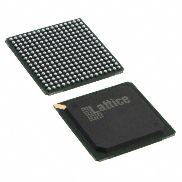
| 产品图片 |
|
| rohs | 符合RoHS无铅 / 符合限制有害物质指令(RoHS)规范要求 |
| 产品系列 | 嵌入式处理器和控制器,FPGA - 现场可编程门阵列,Altera Corporation EP2C15AF256C8NCyclone® II |
| 数据手册 | 点击此处下载产品Datasheet点击此处下载产品Datasheethttp://www.altera.com/literature/ds/pkgds.pdf#page=95-96点击此处下载产品Datasheet |
| 产品型号 | EP2C15AF256C8N |
| 产品 | Cyclone II |
| 产品培训模块 | http://www.digikey.cn/PTM/IndividualPTM.page?site=cn&lang=zhs&ptm=25450 |
| 产品种类 | FPGA - 现场可编程门阵列 |
| 供应商器件封装 | 256-FBGA(17x17) |
| 其它名称 | 544-2098 |
| 商标 | Altera Corporation |
| 安装类型 | 表面贴装 |
| 安装风格 | SMD/SMT |
| 封装 | Tray |
| 封装/外壳 | 256-LBGA |
| 封装/箱体 | FBGA-256 |
| 工作温度 | 0°C ~ 85°C |
| 工作电源电压 | 1.15 V to 1.25 V |
| 工厂包装数量 | 90 |
| 总RAM位数 | 239616 |
| 总内存 | 239616 bit |
| 最大工作温度 | + 70 C |
| 最大工作频率 | 260 MHz |
| 最小工作温度 | 0 C |
| 栅极数 | - |
| 标准包装 | 90 |
| 电压-电源 | 1.15 V ~ 1.25 V |
| 系列 | Cyclone II |
| 输入/输出端数量 | 152 |
| 逻辑元件/单元数 | 14448 |
| 逻辑元件数量 | 14448 |
| 逻辑数组块数量——LAB | 903 |


- 商务部:美国ITC正式对集成电路等产品启动337调查
- 曝三星4nm工艺存在良率问题 高通将骁龙8 Gen1或转产台积电
- 太阳诱电将投资9.5亿元在常州建新厂生产MLCC 预计2023年完工
- 英特尔发布欧洲新工厂建设计划 深化IDM 2.0 战略
- 台积电先进制程称霸业界 有大客户加持明年业绩稳了
- 达到5530亿美元!SIA预计今年全球半导体销售额将创下新高
- 英特尔拟将自动驾驶子公司Mobileye上市 估值或超500亿美元
- 三星加码芯片和SET,合并消费电子和移动部门,撤换高东真等 CEO
- 三星电子宣布重大人事变动 还合并消费电子和移动部门
- 海关总署:前11个月进口集成电路产品价值2.52万亿元 增长14.8%


PDF Datasheet 数据手册内容提取
Cyclone II Device Handbook, Volume 1 101 Innovation Drive San Jose, CA 95134 www.altera.com CII5V1-3.3
Copyright © 2008 Altera Corporation. All rights reserved. Altera, The Programmable Solutions Company, the stylized Altera logo, specific device des- ignations, and all other words and logos that are identified as trademarks and/or service marks are, unless noted otherwise, the trademarks and service marks of Altera Corporation in the U.S. and other countries. All other product or service names are the property of their respective holders. Al- tera products are protected under numerous U.S. and foreign patents and pending applications, maskwork rights, and copyrights. Altera warrants performance of its semiconductor products to current specifications in accordance with Altera's standard warranty, but reserves the right to make changes to any products and services at any time without notice. Altera assumes no responsibility or liability arising out of the ap- plication or use of any information, product, or service described herein except as expressly agreed to in writing by Altera Corporation. Altera customers are advised to obtain the latest version of device specifications before relying on any published in- formation and before placing orders for products or services. ii Altera Corporation
Contents Chapter Revision Dates ........................................................................... xi About This Handbook ............................................................................ xiii How to Contact Altera .......................................................................................................................... xiii Typographic Conventions .................................................................................................................... xiii Section I. Cyclone II Device Family Data Sheet Revision History ....................................................................................................................................1–1 Chapter 1. Introduction Introduction............................................................................................................................................1–1 Low-Cost Embedded Processing Solutions..................................................................................1–1 Low-Cost DSP Solutions .................................................................................................................1–1 Features ...................................................................................................................................................1–2 Referenced Documents .........................................................................................................................1–9 Document Revision History.................................................................................................................1–9 Chapter 2. CycloneII Architecture Functional Description..........................................................................................................................2–1 Logic Elements .......................................................................................................................................2–2 LE Operating Modes........................................................................................................................2–4 Logic Array Blocks ................................................................................................................................2–7 LAB Interconnects ............................................................................................................................2–8 LAB Control Signals.........................................................................................................................2–8 MultiTrack Interconnect .....................................................................................................................2–10 Row Interconnects..........................................................................................................................2–10 Column Interconnects....................................................................................................................2–12 Device Routing ...............................................................................................................................2–15 Global Clock Network & Phase-Locked Loops...............................................................................2–16 Dedicated Clock Pins .....................................................................................................................2–20 Dual-Purpose Clock Pins ..............................................................................................................2–20 Global Clock Network ...................................................................................................................2–21 Global Clock Network Distribution ............................................................................................2–23 PLLs..................................................................................................................................................2–25 Embedded Memory.............................................................................................................................2–27 Memory Modes...............................................................................................................................2–30 Clock Modes....................................................................................................................................2–31 M4K Routing Interface ..................................................................................................................2–31 Altera Corporation iii
Contents Embedded Multipliers ........................................................................................................................2–32 Multiplier Modes............................................................................................................................2–35 Embedded Multiplier Routing Interface.....................................................................................2–36 I/O Structure & Features....................................................................................................................2–37 External Memory Interfacing .......................................................................................................2–44 Programmable Drive Strength .....................................................................................................2–49 Open-Drain Output........................................................................................................................2–50 Slew Rate Control...........................................................................................................................2–51 Bus Hold ..........................................................................................................................................2–51 Programmable Pull-Up Resistor ..................................................................................................2–51 Advanced I/O Standard Support ................................................................................................2–52 High-Speed Differential Interfaces ..............................................................................................2–53 Series On-Chip Termination .........................................................................................................2–55 I/O Banks ........................................................................................................................................2–57 MultiVolt I/O Interface .................................................................................................................2–60 Chapter 3. Configuration & Testing IEEE Std. 1149.1 (JTAG) Boundary Scan Support.............................................................................3–1 Configuration .........................................................................................................................................3–5 Operating Modes ...................................................................................................................................3–5 Configuration Schemes.........................................................................................................................3–6 CycloneII Automated Single Event Upset Detection ......................................................................3–7 Custom-Built Circuitry ....................................................................................................................3–7 Software Interface.............................................................................................................................3–7 Document Revision History.................................................................................................................3–8 Chapter 4. Hot Socketing & Power-On Reset Introduction............................................................................................................................................4–1 CycloneII Hot-Socketing Specifications ............................................................................................4–1 Devices Can Be Driven before Power-Up.....................................................................................4–2 I/O Pins Remain Tri-Stated during Power-Up............................................................................4–2 Hot-Socketing Feature Implementation in CycloneII Devices.......................................................4–3 Power-On Reset Circuitry ....................................................................................................................4–5 "Wake-up" Time for CycloneII Devices .......................................................................................4–5 Conclusion ..............................................................................................................................................4–7 Document Revision History.................................................................................................................4–7 Chapter 5. DC Characteristics and Timing Specifications Operating Conditions ...........................................................................................................................5–1 Single-Ended I/O Standards ..........................................................................................................5–5 Differential I/O Standards..............................................................................................................5–7 DC Characteristics for Different Pin Types ..................................................................................... 5–11 On-Chip Termination Specifications ...........................................................................................5–12 Power Consumption ...........................................................................................................................5–13 Timing Specifications ..........................................................................................................................5–14 Preliminary and Final Timing Specifications .............................................................................5–14 Performance....................................................................................................................................5–15 iv Altera Corporation Cyclone II Device Handbook, Volume1
Contents Internal Timing ...............................................................................................................................5–18 CycloneII Clock Timing Parameters...........................................................................................5–23 Clock Network Skew Adders .......................................................................................................5–29 IOE Programmable Delay .............................................................................................................5–30 Default Capacitive Loading of Different I/O Standards..........................................................5–31 I/O Delays.......................................................................................................................................5–33 Maximum Input and Output Clock Rate....................................................................................5–46 High Speed I/O Timing Specifications .......................................................................................5–55 External Memory Interface Specifications ..................................................................................5–63 JTAG Timing Specifications..........................................................................................................5–64 PLL Timing Specifications ............................................................................................................5–66 Duty Cycle Distortion .........................................................................................................................5–67 DCD Measurement Techniques ...................................................................................................5–68 Referenced Documents .......................................................................................................................5–74 Document Revision History...............................................................................................................5–74 Chapter 6. Reference & Ordering Information Software ..................................................................................................................................................6–1 Device Pin-Outs .....................................................................................................................................6–1 Ordering Information ...........................................................................................................................6–1 Document Revision History.................................................................................................................6–2 Section II. Clock Management Revision History ....................................................................................................................................6–1 Chapter 7. PLLs in CycloneII Devices Introduction............................................................................................................................................7–1 CycloneII PLL Hardware Overview ..................................................................................................7–2 PLL Reference Clock Generation ...................................................................................................7–6 Clock Feedback Modes .......................................................................................................................7–10 Normal Mode..................................................................................................................................7–10 Zero Delay Buffer Mode................................................................................................................7–11 No Compensation Mode ...............................................................................................................7–12 Source-Synchronous Mode ...........................................................................................................7–13 Hardware Features ..............................................................................................................................7–14 Clock Multiplication & Division ..................................................................................................7–14 Programmable Duty Cycle ...........................................................................................................7–15 Phase-Shifting Implementation....................................................................................................7–16 Control Signals................................................................................................................................7–17 Manual Clock Switchover .............................................................................................................7–20 Clocking ................................................................................................................................................7–21 Global Clock Network ...................................................................................................................7–21 Clock Control Block .......................................................................................................................7–24 Global Clock Network Clock Source Generation ......................................................................7–26 Global Clock Network Power Down...........................................................................................7–28 Altera Corporation v Cyclone II Device Handbook, Volume1
Contents clkena signals ..................................................................................................................................7–29 Board Layout ........................................................................................................................................7–30 VCCA & GNDA .............................................................................................................................7–31 VCCD & GND.................................................................................................................................7–33 Conclusion ............................................................................................................................................7–33 Section III. Memory Revision History ....................................................................................................................................7–1 Chapter 8. CycloneII Memory Blocks Introduction............................................................................................................................................8–1 Overview.................................................................................................................................................8–1 Control Signals..................................................................................................................................8–3 Parity Bit Support.............................................................................................................................8–4 Byte Enable Support ........................................................................................................................8–4 Packed Mode Support .....................................................................................................................8–6 Address Clock Enable......................................................................................................................8–6 Memory Modes ......................................................................................................................................8–8 Single-Port Mode..............................................................................................................................8–9 Simple Dual-Port Mode.................................................................................................................8–10 True Dual-Port Mode.....................................................................................................................8–12 Shift Register Mode........................................................................................................................8–14 ROM Mode ......................................................................................................................................8–16 FIFO Buffer Mode...........................................................................................................................8–16 Clock Modes .........................................................................................................................................8–16 Independent Clock Mode..............................................................................................................8–17 Input/Output Clock Mode ...........................................................................................................8–19 Read/Write Clock Mode ...............................................................................................................8–22 Single-Clock Mode .........................................................................................................................8–24 Power-Up Conditions & Memory Initialization ........................................................................8–27 Read-During- Write Operation at the Same Address ....................................................................8–28 Same-Port Read-During-Write Mode..........................................................................................8–28 Mixed-Port Read-During-Write Mode........................................................................................8–29 Conclusion ............................................................................................................................................8–30 Referenced Documents .......................................................................................................................8–30 Chapter 9. External Memory Interfaces Introduction............................................................................................................................................9–1 External Memory Interface Standards................................................................................................9–2 DDR & DDR2 SDRAM ....................................................................................................................9–2 QDRII SRAM.....................................................................................................................................9–5 CycloneII DDR Memory Support Overview ....................................................................................9–9 Data & Data Strobe Pins ................................................................................................................9–10 Clock, Command & Address Pins ...............................................................................................9–14 Parity, DM & ECC Pins .................................................................................................................9–14 vi Altera Corporation Cyclone II Device Handbook, Volume1
Contents Phase Lock Loop (PLL)..................................................................................................................9–15 Clock Delay Control.......................................................................................................................9–15 DQS Postamble ...............................................................................................................................9–16 DDR Input Registers ......................................................................................................................9–18 DDR Output Registers...................................................................................................................9–21 Bidirectional DDR Registers .........................................................................................................9–22 Conclusion ............................................................................................................................................9–24 Document Revision History...............................................................................................................9–25 Section IV. I/O Standards Revision History ....................................................................................................................................9–1 Chapter 10. Selectable I/O Standards in CycloneII Devices Introduction..........................................................................................................................................10–1 Supported I/O Standards...................................................................................................................10–1 3.3-V LVTTL (EIA/JEDEC Standard JESD8-B)..........................................................................10–3 3.3-V LVCMOS (EIA/JEDEC Standard JESD8-B) .....................................................................10–4 3.3-V (PCI Special Interest Group [SIG] PCI Local Bus Specification Revision 3.0) .............10–4 3.3-V PCI-X ......................................................................................................................................10–6 Easy-to-Use, Low-Cost PCI Express Solution ............................................................................10–6 2.5-V LVTTL (EIA/JEDEC Standard EIA/JESD8-5) .................................................................10–7 2.5-V LVCMOS (EIA/JEDEC Standard EIA/JESD8-5) ............................................................10–7 SSTL-2 Class I and II (EIA/JEDEC Standard JESD8-9A) .........................................................10–7 Pseudo-Differential SSTL-2...........................................................................................................10–8 1.8-V LVTTL (EIA/JEDEC Standard EIA/JESD8-7) .................................................................10–9 1.8-V LVCMOS (EIA/JEDEC Standard EIA/JESD8-7) ..........................................................10–10 SSTL-18 Class I and II ..................................................................................................................10–10 1.8-V HSTL Class I and II ............................................................................................................10–11 Pseudo-Differential SSTL-18 Class I and Differential SSTL-18 Class II ...............................10–12 1.8-V Pseudo-Differential HSTL Class I and II ........................................................................10–13 1.5-V LVCMOS (EIA/JEDEC Standard JESD8-11)..................................................................10–14 1.5-V HSTL Class I and II ............................................................................................................10–14 1.5-V Pseudo-Differential HSTL Class I and II ........................................................................10–15 LVDS, RSDS and mini-LVDS .....................................................................................................10–16 Differential LVPECL ....................................................................................................................10–17 CycloneII I/O Banks ........................................................................................................................10–18 Programmable Current Drive Strength..........................................................................................10–24 Voltage-Referenced I/O Standard Termination ......................................................................10–26 Differential I/O Standard Termination ....................................................................................10–26 I/O Driver Impedance Matching (R ) and Series Termination (R ) .....................................10–27 S S Pad Placement and DC Guidelines .................................................................................................10–27 Differential Pad Placement Guidelines .....................................................................................10–28 V Pad Placement Guidelines .................................................................................................10–29 REF DC Guidelines...............................................................................................................................10–32 5.0-V Device Compatibility ..............................................................................................................10–34 Altera Corporation vii Cyclone II Device Handbook, Volume1
Contents Conclusion ..........................................................................................................................................10–36 References ...........................................................................................................................................10–37 Referenced Documents .....................................................................................................................10–38 Document Revision History.............................................................................................................10–38 Chapter 11. High-Speed Differential Interfaces in CycloneII Devices Introduction..........................................................................................................................................11–1 CycloneII High-Speed I/O Banks ....................................................................................................11–1 CycloneII High-Speed I/O Interface ...............................................................................................11–3 I/O Standards Support .......................................................................................................................11–4 LVDS Standard Support in CycloneII Devices .........................................................................11–4 RSDS I/O Standard Support in CycloneII Devices ..................................................................11–7 mini-LVDS Standard Support in CycloneII Devices................................................................11–9 LVPECL Support in CycloneII ..................................................................................................11–11 Differential SSTL Support in CycloneII Devices.....................................................................11–12 Differential HSTL Support in CycloneII Devices ...................................................................11–13 High-Speed I/O Timing in CycloneII Devices.............................................................................11–14 Design Guidelines .............................................................................................................................11–16 Differential Pad Placement Guidelines .....................................................................................11–16 Board Design Considerations .....................................................................................................11–16 Conclusion ..........................................................................................................................................11–17 Section V. DSP Revision History ..................................................................................................................................11–1 Chapter 12. Embedded Multipliers in Cyclone II Devices Introduction..........................................................................................................................................12–1 Embedded Multiplier Block Overview ............................................................................................12–2 Architecture ..........................................................................................................................................12–4 Input Registers................................................................................................................................12–4 Multiplier Stage ..............................................................................................................................12–5 Output Registers.............................................................................................................................12–6 Operational Modes ..............................................................................................................................12–6 18-Bit Multipliers............................................................................................................................12–7 9-Bit Multipliers..............................................................................................................................12–7 Software Support .................................................................................................................................12–9 Conclusion ............................................................................................................................................12–9 Section VI. Configuration & Test Revision History ..................................................................................................................................12–1 Chapter 13. Configuring CycloneII Devices Introduction..........................................................................................................................................13–1 viii Altera Corporation Cyclone II Device Handbook, Volume1
Contents CycloneII Configuration Overview .................................................................................................13–1 Configuration File Format..................................................................................................................13–3 Configuration Data Compression .....................................................................................................13–3 Active Serial Configuration (Serial Configuration Devices) .........................................................13–6 Single Device AS Configuration...................................................................................................13–7 Multiple Device AS Configuration ............................................................................................13–12 Configuring Multiple CycloneII Devices with the Same Design .........................................13–15 Estimating AS Configuration Time ...........................................................................................13–18 Programming Serial Configuration Devices ............................................................................13–19 PS Configuration................................................................................................................................13–22 Single Device PS Configuration Using a MAXII Device as an External Host ....................13–22 Multiple Device PS Configuration Using a MAXII Device as an External Host................13–26 PS Configuration Using a Microprocessor ...............................................................................13–31 Single Device PS Configuration Using a Configuration Device............................................13–32 Multiple Device PS Configuration Using a Configuration Device .......................................13–37 PS Configuration Using a Download Cable .............................................................................13–48 JTAG Configuration ..........................................................................................................................13–53 Single Device JTAG Configuration............................................................................................13–55 JTAG Configuration of Multiple Devices .................................................................................13–58 Jam STAPL ....................................................................................................................................13–60 Configuring CycloneII FPGAs with JRunner..........................................................................13–60 Combining JTAG & Active Serial Configuration Schemes ....................................................13–61 Programming Serial Configuration Devices In-System Using the JTAG Interface ............13–61 Device Configuration Pins ...............................................................................................................13–64 Conclusion ..........................................................................................................................................13–70 Chapter 14. IEEE 1149.1 (JTAG) Boundary-Scan Testing for CycloneII Devices Introduction..........................................................................................................................................14–1 IEEE Std. 1149.1 BST Architecture ....................................................................................................14–2 IEEE Std. 1149.1 Boundary-Scan Register ........................................................................................14–4 Boundary-Scan Cells of a CycloneII Device I/O Pin ...............................................................14–4 IEEE Std. 1149.1 BST Operation Control ..........................................................................................14–6 SAMPLE/PRELOAD Instruction Mode .....................................................................................14–9 Capture Phase ...............................................................................................................................14–10 Shift & Update Phases .................................................................................................................14–10 EXTEST Instruction Mode ..........................................................................................................14–11 Capture Phase ...............................................................................................................................14–12 Shift & Update Phases .................................................................................................................14–12 BYPASS Instruction Mode ..........................................................................................................14–13 IDCODE Instruction Mode .........................................................................................................14–14 USERCODE Instruction Mode ...................................................................................................14–14 CLAMP Instruction Mode ..........................................................................................................14–14 HIGHZ Instruction Mode ...........................................................................................................14–15 I/O Voltage Support in JTAG Chain.........................................................................................14–15 Using IEEE Std. 1149.1 BST Circuitry .............................................................................................14–16 BST for Configured Devices.............................................................................................................14–17 Disabling IEEE Std. 1149.1 BST Circuitry.......................................................................................14–18 Altera Corporation ix Cyclone II Device Handbook, Volume1
Contents Guidelines for IEEE Std. 1149.1 Boundary-Scan Testing .............................................................14–18 Boundary-Scan Description Language (BSDL) Support..............................................................14–19 Conclusion ..........................................................................................................................................14–19 References ...........................................................................................................................................14–19 Document Revision History.............................................................................................................14–20 Section VII. PCB Layout Guidelines Revision History ..................................................................................................................................14–1 Chapter 15. Package Information for CycloneII Devices Introduction..........................................................................................................................................15–1 Thermal Resistance..............................................................................................................................15–2 Package Outlines .................................................................................................................................15–4 144-Pin Plastic Thin Quad Flat Pack (TQFP) – Wirebond ........................................................15–4 208-Pin Plastic Quad Flat Pack (PQFP) – Wirebond .................................................................15–7 240-Pin Plastic Quad Flat Pack (PQFP) .......................................................................................15–9 256-Pin FineLine Ball-Grid Array, Option 2 – Wirebond .......................................................15–11 484-Pin FineLine BGA, Option 3 – Wirebond ..........................................................................15–13 484-Pin Ultra FineLine BGA – Wirebond .................................................................................15–15 672-Pin FineLine BGA Package, Option 3 – Wirebond...........................................................15–17 896-Pin FineLine BGA Package – Wirebond ............................................................................15–19 x Altera Corporation Cyclone II Device Handbook, Volume1
Chapter Revision Dates The chapters in this book, Cyclone II Device Handbook, Volume1, were revised on the following dates. Where chapters or groups of chapters are available separately, part numbers are listed. Chapter 1. Introduction Revised: February 2008 Part number: CII51001-3.2 Chapter 2. CycloneII Architecture Revised: February 2007 Part number: CII51002-3.1 Chapter 3. Configuration & Testing Revised: February 2007 Part number: CII51003-2.2 Chapter 4. Hot Socketing & Power-On Reset Revised: February 2007 Part number: CII51004-3.1 Chapter 5. DC Characteristics and Timing Specifications Revised: February 2008 Part number: CII51005-4.0 Chapter 6. Reference & Ordering Information Revised: February 2007 Part number: CII51006-1.4 Chapter 7. PLLs in CycloneII Devices Revised: February 2007 Part number: CII51007-3.1 Chapter 8. CycloneII Memory Blocks Revised: February 2008 Part number: CII51008-2.4 Chapter 9. External Memory Interfaces Revised: February 2007 Part number: CII51009-3.1 Altera Corporation xi
Chapter Revision Dates Cyclone II Device Handbook, Volume1 Chapter 10. Selectable I/O Standards in CycloneII Devices Revised: February 2008 Part number: CII51010-2.4 Chapter 11. High-Speed Differential Interfaces in CycloneII Devices Revised: February 2007 Part number: CII51011-2.2 Chapter 12. Embedded Multipliers in Cyclone II Devices Revised: February 2007 Part number: CII51012-1.2 Chapter 13. Configuring CycloneII Devices Revised: February 2007 Part number: CII51013-3.1 Chapter 14. IEEE 1149.1 (JTAG) Boundary-Scan Testing for CycloneII Devices Revised: February 2007 Part number: CII51014-2.1 Chapter 15. Package Information for CycloneII Devices Revised: February 2007 Part number: CII51015-2.3 xii Altera Corporation
About This Handbook This handbook provides comprehensive information about the Altera® Cyclone®II family of devices. How to Contact For the most up-to-date information about Altera products, refer to the following table. Altera Contact Contact (1) Address Method Technical support Website www.altera.com/support Technical training Website www.altera.com/training Email custrain@altera.com Product literature Website www.altera.com/literature Altera literature services Email literature@altera.com Non-technical support (General) Email nacomp@altera.com (Software Licensing) Email authorization@altera.com Note to table: (1) You can also contact your local Altera sales office or sales representative. Typographic This document uses the typographic conventions shown below. Conventions Visual Cue Meaning Bold Type with Initial Command names, dialog box titles, checkbox options, and dialog box options are Capital Letters shown in bold, initial capital letters. Example: Save As dialog box. bold type External timing parameters, directory names, project names, disk drive names, filenames, filename extensions, and software utility names are shown in bold type. Examples: f , \qdesigns directory, d: drive, chiptrip.gdf file. MAX Italic Type with Initial Capital Document titles are shown in italic type with initial capital letters. Example: AN Letters 75: High-Speed Board Design. Altera Corporation xiii Cyclone II Device Handbook, Volume 1
Typographic Conventions Visual Cue Meaning Italic type Internal timing parameters and variables are shown in italic type. Examples: t , n + 1. PIA Variable names are enclosed in angle brackets (< >) and shown in italic type. Example: <file name>, <project name>.pof file. Initial Capital Letters Keyboard keys and menu names are shown with initial capital letters. Examples: Delete key, the Options menu. “Subheading Title” References to sections within a document and titles of on-line help topics are shown in quotation marks. Example: “Typographic Conventions.” Courier type Signal and port names are shown in lowercase Courier type. Examples: data1, tdi, input. Active-low signals are denoted by suffix n, e.g., resetn. Anything that must be typed exactly as it appears is shown in Courier type. For example: c:\qdesigns\tutorial\chiptrip.gdf. Also, sections of an actual file, such as a Report File, references to parts of files (e.g., the AHDL keyword SUBDESIGN), as well as logic function names (e.g., TRI) are shown in Courier. 1., 2., 3., and Numbered steps are used in a list of items when the sequence of the items is a., b., c., etc. important, such as the steps listed in a procedure. ■ ● (cid:129) Bullets are used in a list of items when the sequence of the items is not important. v The checkmark indicates a procedure that consists of one step only. 1 The hand points to information that requires special attention. The caution indicates required information that needs special consideration and c understanding and should be read prior to starting or continuing with the procedure or process. w The warning indicates information that should be read prior to starting or continuing the procedure or processes r The angled arrow indicates you should press the Enter key. f The feet direct you to more information on a particular topic. xiv Altera Corporation Cyclone II Device Handbook, Volume 1
Section I. Cyclone II Device Family Data Sheet This section provides information for board layout designers to successfully layout their boards for Cyclone®II devices. It contains the required PCB layout guidelines, device pin tables, and package specifications. This section includes the following chapters: ■ Chapter1. Introduction ■ Chapter2. CycloneII Architecture ■ Chapter3. Configuration & Testing ■ Chapter4. Hot Socketing & Power-On Reset ■ Chapter5. DC Characteristics and Timing Specifications ■ Chapter6. Reference & Ordering Information Revision History Refer to each chapter for its own specific revision history. For information on when each chapter was updated, refer to the Chapter Revision Dates section, which appears in the complete handbook. Altera Corporation Section I–1 Preliminary
Revision History Cyclone II Device Handbook, Volume 1 Section I–2 Altera Corporation Preliminary
1. Introduction CII51001-3.2 Introduction Following the immensely successful first-generation Cyclone® device family, Altera® CycloneII FPGAs extend the low-cost FPGA density range to 68,416 logic elements (LEs) and provide up to 622 usable I/O pins and up to 1.1 Mbits of embedded memory. Cyclone II FPGAs are manufactured on 300-mm wafers using TSMC's 90-nm low-k dielectric process to ensure rapid availability and low cost. By minimizing silicon area, Cyclone II devices can support complex digital systems on a single chip at a cost that rivals that of ASICs. Unlike other FPGA vendors who compromise power consumption and performance for low-cost, Altera’s latest generation of low-cost FPGAs—Cyclone II FPGAs, offer 60% higher performance and half the power consumption of competing 90-nm FPGAs. The low cost and optimized feature set of CycloneII FPGAs make them ideal solutions for a wide array of automotive, consumer, communications, video processing, test and measurement, and other end-market solutions. Reference designs, system diagrams, and IP, found at www.altera.com, are available to help you rapidly develop complete end-market solutions using CycloneII FPGAs. Low-Cost Embedded Processing Solutions Cyclone II devices support the Nios II embedded processor which allows you to implement custom-fit embedded processing solutions. Cyclone II devices can also expand the peripheral set, memory, I/O, or performance of embedded processors. Single or multiple Nios II embedded processors can be designed into a Cyclone II device to provide additional co-processing power or even replace existing embedded processors in your system. Using Cyclone II and Nios II together allow for low-cost, high-performance embedded processing solutions, which allow you to extend your product's life cycle and improve time to market over standard product solutions. Low-Cost DSP Solutions Use Cyclone II FPGAs alone or as DSP co-processors to improve price-to-performance ratios for digital signal processing (DSP) applications. You can implement high-performance yet low-cost DSP systems with the following Cyclone II features and design support: ■ Up to 150 18 × 18 multipliers ■ Up to 1.1 Mbit of on-chip embedded memory ■ High-speed interfaces to external memory Altera Corporation 1–1 February 2008
Features ■ DSP intellectual property (IP) cores ■ DSP Builder interface to The Mathworks Simulink and Matlab design environment ■ DSP Development Kit, Cyclone II Edition Cyclone II devices include a powerful FPGA feature set optimized for low-cost applications including a wide range of density, memory, embedded multiplier, and packaging options. Cyclone II devices support a wide range of common external memory interfaces and I/O protocols required in low-cost applications. Parameterizable IP cores from Altera and partners make using Cyclone II interfaces and protocols fast and easy. Features The Cyclone II device family offers the following features: ■ High-density architecture with 4,608 to 68,416 LEs ● M4K embedded memory blocks ● Up to 1.1 Mbits of RAM available without reducing available logic ● 4,096 memory bits per block (4,608 bits per block including 512 parity bits) ● Variable port configurations of ×1, ×2, ×4, ×8, ×9, ×16, ×18, ×32, and ×36 ● True dual-port (one read and one write, two reads, or two writes) operation for ×1, ×2, ×4, ×8, ×9, ×16, and ×18 modes ● Byte enables for data input masking during writes ● Up to 260-MHz operation ■ Embedded multipliers ● Up to 150 18- × 18-bit multipliers are each configurable as two independent 9- × 9-bit multipliers with up to 250-MHz performance ● Optional input and output registers ■ Advanced I/O support ● High-speed differential I/O standard support, including LVDS, RSDS, mini-LVDS, LVPECL, differential HSTL, and differential SSTL ● Single-ended I/O standard support, including 2.5-V and 1.8-V, SSTL class I and II, 1.8-V and 1.5-V HSTL class I and II, 3.3-V PCI and PCI-X 1.0, 3.3-, 2.5-, 1.8-, and 1.5-V LVCMOS, and 3.3-, 2.5-, and 1.8-V LVTTL ● Peripheral Component Interconnect Special Interest Group (PCI SIG) PCI Local Bus Specification, Revision 3.0 compliance for 3.3-V operation at 33 or 66 MHz for 32- or 64-bit interfaces ● PCI Express with an external TI PHY and an Altera PCI Express ×1 Megacore® function 1–2 Altera Corporation Cyclone II Device Handbook, Volume 1 February 2008
Introduction ● 133-MHz PCI-X 1.0 specification compatibility ● High-speed external memory support, including DDR, DDR2, and SDR SDRAM, and QDRII SRAM supported by drop in Altera IP MegaCore functions for ease of use ● Three dedicated registers per I/O element (IOE): one input register, one output register, and one output-enable register ● Programmable bus-hold feature ● Programmable output drive strength feature ● Programmable delays from the pin to the IOE or logic array ● I/O bank grouping for unique VCCIO and/or VREF bank settings ● MultiVolt™ I/O standard support for 1.5-, 1.8-, 2.5-, and 3.3-interfaces ● Hot-socketing operation support ● Tri-state with weak pull-up on I/O pins before and during configuration ● Programmable open-drain outputs ● Series on-chip termination support ■ Flexible clock management circuitry ● Hierarchical clock network for up to 402.5-MHz performance ● Up to four PLLs per device provide clock multiplication and division, phase shifting, programmable duty cycle, and external clock outputs, allowing system-level clock management and skew control ● Up to 16 global clock lines in the global clock network that drive throughout the entire device ■ Device configuration ● Fast serial configuration allows configuration times less than 100 ms ● Decompression feature allows for smaller programming file storage and faster configuration times ● Supports multiple configuration modes: active serial, passive serial, and JTAG-based configuration ● Supports configuration through low-cost serial configuration devices ● Device configuration supports multiple voltages (either 3.3, 2.5, or 1.8 V) ■ Intellectual property ● Altera megafunction and Altera MegaCore function support, and Altera Megafunctions Partners Program (AMPPSM) megafunction support, for a wide range of embedded processors, on-chip and off-chip interfaces, peripheral functions, DSP functions, and communications functions and Altera Corporation 1–3 February 2008 Cyclone II Device Handbook, Volume 1
Features protocols. Visit the Altera IPMegaStore at www.altera.com to download IP MegaCore functions. ● Nios II Embedded Processor support The Cyclone II family offers devices with the Fast-On feature, which offers a faster power-on-reset (POR) time. Devices that support the Fast-On feature are designated with an “A” in the device ordering code. For example, EP2C5A, EP2C8A, EP2C15A, and EP2C20A. The EP2C5A is only available in the automotive speed grade. The EP2C8A and EP2C20A are only available in the industrial speed grade. The EP2C15A is only available with the Fast-On feature and is available in both commercial and industrial grades. The Cyclone II “A” devices are identical in feature set and functionality to the non-A devices except for support of the faster POR time. f Cyclone II A devices are offered in automotive speed grade. For more information, refer to the Cyclone II section in the Automotive-Grade Device Handbook. f For more information on POR time specifications for CycloneII A and non-A devices, refer to the Hot Socketing & Power-On Reset chapter in the CycloneII Device Handbook. Table1–1 lists the CycloneII device family features. Table1–2 lists the CycloneII device package offerings and maximum user I/O pins. Table1–1.CycloneII FPGA Family Features (Part 1 of2) Feature EP2C5 (2) EP2C8 (2) EP2C15 (1) EP2C20 (2) EP2C35 EP2C50 EP2C70 LEs 4,608 8,256 14,448 18,752 33,216 50,528 68,416 M4K RAM blocks (4 26 36 52 52 105 129 250 Kbits plus 512parity bits Total RAM bits 119,808 165,888 239,616 239,616 483,840 594,432 1,152,00 0 Embedded 13 18 26 26 35 86 150 multipliers (3) PLLs 2 2 4 4 4 4 4 1–4 Altera Corporation Cyclone II Device Handbook, Volume 1 February 2008
Introduction Table1–1.CycloneII FPGA Family Features (Part 2 of2) Feature EP2C5 (2) EP2C8 (2) EP2C15 (1) EP2C20 (2) EP2C35 EP2C50 EP2C70 Maximum user 158 182 315 315 475 450 622 I/Opins Notes to Table1–1: (1) The EP2C15A is only available with the Fast On feature, which offers a faster POR time. This device is available in both commercial and industrial grade. (2) The EP2C5, EP2C8, and EP2C20 optionally support the Fast On feature, which is designated with an “A” in the device ordering code. The EP2C5A is only available in the automotive speed grade. The EP2C8A and EP2C20A devices are only available in industrial grade. (3) This is the total number of 18 × 18 multipliers. For the total number of 9 × 9 multipliers per device, multiply the total number of 18 × 18 multipliers by 2. Altera Corporation 1–5 February 2008 Cyclone II Device Handbook, Volume 1
Features Table1–2.CycloneII Package Options & Maximum User I/O Pins Notes(1) (2) 484-Pin 256-Pin 484-Pin 672-Pin 896-Pin 144-Pin 208-Pin 240-Pin Ultra Device FineLine FineLine FineLine FineLine TQFP (3) PQFP (4) PQFP FineLine BGA BGA BGA BGA BGA EP2C5 (6) (8) 89 142 — 158 (5) — — — — EP2C8 (6) 85 138 — 182 — — — — EP2C8A (6), (7) — — — 182 — — — — EP2C15A (6), (7) — — — 152 315 — — — EP2C20 (6) — — 142 152 315 — — — EP2C20A (6), (7) — — — 152 315 — — — EP2C35 (6) — — — — 322 322 475 — EP2C50 (6) — — — — 294 294 450 — EP2C70 (6) — — — — — — 422 622 Notes to Table1–2: (1) CycloneII devices support vertical migration within the same package (for example, you can migrate between the EP2C20 device in the 484-pin FineLine BGA package and the EP2C35 and EP2C50 devices in the same package). (2) The Quartus® II software I/O pin counts include four additional pins, TDI, TDO, TMS, and TCK, which are not available as general purpose I/O pins. (3) TQFP: thin quad flat pack. (4) PQFP: plastic quad flat pack. (5) Vertical migration is supported between the EP2C5F256 and the EP2C8F256 devices. However, not all of the DQ and DQS groups are supported. Vertical migration between the EP2C5 and the EP2C15 in the F256 package is not supported. (6) The I/O pin counts for the EP2C5, EP2C8, and EP2C15A devices include 8 dedicated clock pins that can be used for data inputs. The I/O counts for the EP2C20, EP2C35, EP2C50, and EP2C70 devices include 16 dedicated clock pins that can be used for data inputs. (7) EP2C8A, EP2C15A, and EP2C20A have a Fast On feature that has a faster POR time. The EP2C15A is only available with the Fast On option. (8) The EP2C5 optionally support the Fast On feature, which is designated with an “A” in the device ordering code. The EP2C5A is only available in the automotive speed grade. Refer to the Cyclone II section in the Automotive-Grade Device Handbook. CycloneII devices support vertical migration within the same package (for example, you can migrate between the EP2C35, EPC50, and EP2C70 devices in the 672-pin FineLine BGA package). The exception to vertical migration support within the CycloneII family is noted in Table1–3. 1–6 Altera Corporation Cyclone II Device Handbook, Volume 1 February 2008
Introduction Vertical migration means that you can migrate to devices whose dedicated pins, configuration pins, and power pins are the same for a given package across device densities. Table1–3.Total Number of Non-Migratable I/O Pins for CycloneII Vertical Migration Paths 256-Pin 484-Pin 672-Pin Vertical 208-Pin 484-Pin Ultra 144-Pin TQFP FineLine BGA FineLine BGA FineLine BGA Migration Path PQFP FineLine BGA (1) (2) (3) EP2C5 to 4 4 1 (4) — — — EP2C8 EP2C8 to — — 30 — — — EP2C15 EP2C15 to — — 0 0 — — EP2C20 EP2C20 to — — 16 — — EP2C35 EP2C35 to — — — 28 28 (5) 28 EP2C50 EP2C50 to — — — — 28 28 EP2C70 Notes to Table1–3: (1) Vertical migration between the EP2C5F256 to the EP2C15AF256 and the EP2C5F256 to the EP2C20F256 devices is not supported. (2) When migrating from the EP2C20F484 device to the EP2C50F484 device, a total of 39 I/O pins are non-migratable. (3) When migrating from the EP2C35F672 device to the EP2C70F672 device, a total of 56 I/O pins are non-migratable. (4) In addition to the one non-migratable I/O pin, there are 34 DQ pins that are non-migratable. (5) The pinouts of 484 FBGA and 484 UBGA are the same. 1 When moving from one density to a larger density, I/O pins are often lost because of the greater number of power and ground pins required to support the additional logic within the larger device. For I/O pin migration across densities, you must cross reference the available I/O pins using the device pin-outs for all planned densities of a given package type to identify which I/O pins are migratable. To ensure that your board layout supports migratable densities within one package offering, enable the applicable vertical migration path within the QuartusII software (go to Assignments menu, then Device, then click the Migration Devices button). After compilation, check the information messages for a full list of I/O, DQ, LVDS, and other pins that are not available because of the selected migration path. Table1–3 lists the CycloneII device package offerings and shows the total number of non-migratable I/O pins when migrating from one density device to a larger density device. Altera Corporation 1–7 February 2008 Cyclone II Device Handbook, Volume 1
Features CycloneII devices are available in up to three speed grades: –6, –7, and –8, with –6 being the fastest. Table1–4 shows the CycloneII device speed-grade offerings. Table1–4.CycloneII Device Speed Grades 484-Pin 256-Pin 484-Pin 672-Pin 896-Pin 144-Pin 208-Pin 240-Pin Ultra Device FineLine FineLine FineLine FineLine TQFP PQFP PQFP FineLine BGA BGA BGA BGA BGA EP2C5 (1) –6, –7, –8 –7, –8 — –6, –7, –8 — — — — EP2C8 –6, –7, –8 –7, –8 — –6, –7, –8 — — — — EP2C8A (2) — — — –8 — — — — EP2C15A — — — –6, –7, –8 –6, –7, –8 — — — EP2C20 — — –8 –6, –7, –8 –6, –7, –8 — — — EP2C20A (2) — — — –8 –8 — — — EP2C35 — — — — –6, –7, –8 –6, –7, –8 –6, –7, –8 — EP2C50 — — — — –6, –7, –8 –6, –7, –8 –6, –7, –8 — EP2C70 — — — — — — –6, –7, –8 –6, –7, –8 Notes to Table1–4: (1) The EP2C5 optionally support the Fast On feature, which is designated with an “A” in the device ordering code. The EP2C5A is only available in the automotive speed grade. Refer to the Cyclone II section in the Automotive-Grade Device Handbook for detailed information. (2) EP2C8A and EP2C20A are only available in industrial grade. 1–8 Altera Corporation Cyclone II Device Handbook, Volume 1 February 2008
Introduction Referenced This chapter references the following documents: Documents ■ Hot Socketing & Power-On Reset chapter in Cyclone II Device Handbook ■ Automotive-Grade Device Handbook Document Table1–5 shows the revision history for this document. Revision History Table1–5.Document Revision History Date & Document Changes Made Summary of Changes Version February 2008 ● Added “Referenced Documents”. — v3.2 ● Updated “Features” section and Table1–1, Table1–2, and Table1–4 with information about EP2C5A. February 2007 ● Added document revision history. Note to explain difference v3.1 ● Added new Note(2) to Table1–2. between I/O pin count information provided in Table1–2 and in the Quartus II software documentation. November 2005 ● Updated Introduction and Features. — v2.1 ● Updated Table1–3. July 2005 v2.0 ● Updated technical content throughout. — ● Updated Table1–2. ● Added Tables1–3 and 1–4. November 2004 ● Updated Table1–2. — v1.1 ● Updated bullet list in the “Features” section. June 2004 v1.0 Added document to the CycloneII Device Handbook. — Altera Corporation 1–9 February 2008 Cyclone II Device Handbook, Volume 1
Document Revision History 1–10 Altera Corporation Cyclone II Device Handbook, Volume 1 February 2008
2. CycloneII Architecture CII51002-3.1 Functional Cyclone®II devices contain a two-dimensional row- and column-based architecture to implement custom logic. Column and row interconnects Description of varying speeds provide signal interconnects between logic array blocks (LABs), embedded memory blocks, and embedded multipliers. The logic array consists of LABs, with 16 logic elements (LEs) in each LAB. An LE is a small unit of logic providing efficient implementation of user logic functions. LABs are grouped into rows and columns across the device. CycloneII devices range in density from 4,608 to 68,416 LEs. CycloneII devices provide a global clock network and up to four phase-locked loops (PLLs). The global clock network consists of up to 16 global clock lines that drive throughout the entire device. The global clock network can provide clocks for all resources within the device, such as input/output elements (IOEs), LEs, embedded multipliers, and embedded memory blocks. The global clock lines can also be used for other high fan-out signals. CycloneII PLLs provide general-purpose clocking with clock synthesis and phase shifting as well as external outputs for high-speed differential I/O support. M4K memory blocks are true dual-port memory blocks with 4K bits of memory plus parity (4,608 bits). These blocks provide dedicated true dual-port, simple dual-port, or single-port memory up to 36-bits wide at up to 260 MHz. These blocks are arranged in columns across the device in between certain LABs. CycloneII devices offer between 119 to 1,152Kbits of embedded memory. Each embedded multiplier block can implement up to either two 9 × 9-bit multipliers, or one 18 × 18-bit multiplier with up to 250-MHz performance. Embedded multipliers are arranged in columns across the device. Each CycloneII device I/O pin is fed by an IOE located at the ends of LAB rows and columns around the periphery of the device. I/O pins support various single-ended and differential I/O standards, such as the 66- and 33-MHz, 64- and 32-bit PCI standard, PCI-X, and the LVDS I/O standard at a maximum data rate of 805 megabits per second (Mbps) for inputs and 640 Mbps for outputs. Each IOE contains a bidirectional I/O buffer and three registers for registering input, output, and output-enable signals. Dual-purpose DQS, DQ, and DM pins along with delay chains (used to Altera Corporation 2–1 February 2007
Logic Elements phase-align double data rate (DDR) signals) provide interface support for external memory devices such as DDR, DDR2, and single data rate (SDR) SDRAM, and QDRII SRAM devices at up to 167 MHz. Figure2–1 shows a diagram of the CycloneII EP2C20 device. Figure2–1.CycloneII EP2C20 Device Block Diagram PLL IOEs PLL Embedded Multipliers Logic Logic Logic Logic IOEs IOEs Array Array Array Array M4K Blocks M4K Blocks PLL IOEs PLL The number of M4K memory blocks, embedded multiplier blocks, PLLs, rows, and columns vary per device. Logic Elements The smallest unit of logic in the CycloneII architecture, the LE, is compact and provides advanced features with efficient logic utilization. Each LE features: ■ A four-input look-up table (LUT), which is a function generator that can implement any function of four variables ■ A programmable register ■ A carry chain connection ■ A register chain connection ■ The ability to drive all types of interconnects: local, row, column, register chain, and direct link interconnects ■ Support for register packing ■ Support for register feedback 2–2 Altera Corporation Cyclone II Device Handbook, Volume 1 February 2007
CycloneII Architecture Figure2–2 shows a CycloneII LE. Figure2–2.CycloneII LE Register Chain Routing From Previous LE LAB-Wide Register Bypass Synchronous LAB Carry-In Load Programmable LAB-Wide Packed Register Synchronous Register Select Clear data1 Row, Column, ddaattaa23 LoToakb-leUp CChaarriny SyLnocahdr oannodus D Q ARnodu tDinigrect Link (LUT) Clear Logic data4 ENA CLRN Row, Column, And Direct Link Routing labclr1 labclr2 Asynchronous Clear Logic Local Routing Chip-Wide Reset (DEV_CLRn) Register Chain Clock & Register Output Clock Enable Feedback Select labclk1 labclk2 labclkena1 labclkena2 LAB Carry-Out Each LE’s programmable register can be configured for D, T, JK, or SR operation. Each register has data, clock, clock enable, and clear inputs. Signals that use the global clock network, general-purpose I/O pins, or any internal logic can drive the register’s clock and clear control signals. Either general-purpose I/O pins or internal logic can drive the clock enable. For combinational functions, the LUT output bypasses the register and drives directly to the LE outputs. Each LE has three outputs that drive the local, row, and column routing resources. The LUT or register output can drive these three outputs independently. Two LE outputs drive column or row and direct link routing connections and one drives local interconnect resources, allowing the LUT to drive one output while the register drives another output. This feature, register packing, improves device utilization because the device can use the register and the LUT for unrelated functions. When using register packing, the LAB-wide synchronous load control signal is not available. See “LAB Control Signals” on page2–8 for more information. Altera Corporation 2–3 February 2007 Cyclone II Device Handbook, Volume 1
Logic Elements Another special packing mode allows the register output to feed back into the LUT of the same LE so that the register is packed with its own fan-out LUT, providing another mechanism for improved fitting. The LE can also drive out registered and unregistered versions of the LUT output. In addition to the three general routing outputs, the LEs within an LAB have register chain outputs. Register chain outputs allow registers within the same LAB to cascade together. The register chain output allows an LAB to use LUTs for a single combinational function and the registers to be used for an unrelated shift register implementation. These resources speed up connections between LABs while saving local interconnect resources. See “MultiTrack Interconnect” on page2–10 for more information on register chain connections. LE Operating Modes The CycloneII LE operates in one of the following modes: ■ Normal mode ■ Arithmetic mode Each mode uses LE resources differently. In each mode, six available inputs to the LE—the four data inputs from the LAB local interconnect, the LAB carry-in from the previous carry-chain LAB, and the register chain connection—are directed to different destinations to implement the desired logic function. LAB-wide signals provide clock, asynchronous clear, synchronous clear, synchronous load, and clock enable control for the register. These LAB-wide signals are available in all LE modes. The Quartus®II software, in conjunction with parameterized functions such as library of parameterized modules (LPM) functions, automatically chooses the appropriate mode for common functions such as counters, adders, subtractors, and arithmetic functions. If required, you can also create special-purpose functions that specify which LE operating mode to use for optimal performance. Normal Mode The normal mode is suitable for general logic applications and combinational functions. In normal mode, four data inputs from the LAB local interconnect are inputs to a four-input LUT (see Figure2–3). The QuartusII Compiler automatically selects the carry-in or the data3 signal as one of the inputs to the LUT. LEs in normal mode support packed registers and register feedback. 2–4 Altera Corporation Cyclone II Device Handbook, Volume 1 February 2007
CycloneII Architecture Figure2–3.LE in Normal Mode sload sclear (LAB Wide) (LAB Wide) Packed Register Input Register chain connection Q Row, Column, and data1 D Direct Link Routing data2 Row, Column, and ENA data3 Four-Input CLRN Direct Link Routing cin (from cout LUT of previous LE) clock (LAB Wide) Local routing data4 ena (LAB Wide) aclr (LAB Wide) Register Register Feedback chain output Arithmetic Mode The arithmetic mode is ideal for implementing adders, counters, accumulators, and comparators. An LE in arithmetic mode implements a 2-bit full adder and basic carry chain (see Figure2–4). LEs in arithmetic mode can drive out registered and unregistered versions of the LUT output. Register feedback and register packing are supported when LEs are used in arithmetic mode. Altera Corporation 2–5 February 2007 Cyclone II Device Handbook, Volume 1
Logic Elements Figure2–4.LE in Arithmetic Mode sload sclear (LAB Wide) (LAB Wide) Register chain connection data1 data2 Three-Input Q Row, column, and LUT D direct link routing Row, column, and ENA CLRN direct link routing cin (from cout Three-Input clock (LAB Wide) of previous LE) LUT ena (LAB Wide) Local routing aclr (LAB Wide) cout Register chain output Register Feedback The QuartusII Compiler automatically creates carry chain logic during design processing, or you can create it manually during design entry. Parameterized functions such as LPM functions automatically take advantage of carry chains for the appropriate functions. The QuartusII Compiler creates carry chains longer than 16 LEs by automatically linking LABs in the same column. For enhanced fitting, a long carry chain runs vertically, which allows fast horizontal connections to M4K memory blocks or embedded multipliers through direct link interconnects. For example, if a design has a long carry chain in a LAB column next to a column of M4K memory blocks, any LE output can feed an adjacent M4K memory block through the direct link interconnect. Whereas if the carry chains ran horizontally, any LAB not next to the column of M4K memory blocks would use other row or column interconnects to drive a M4K memory block. A carry chain continues as far as a full column. 2–6 Altera Corporation Cyclone II Device Handbook, Volume 1 February 2007
CycloneII Architecture Logic Array Each LAB consists of the following: Blocks ■ 16 LEs ■ LAB control signals ■ LE carry chains ■ Register chains ■ Local interconnect The local interconnect transfers signals between LEs in the same LAB. Register chain connections transfer the output of one LE’s register to the adjacent LE’s register within an LAB. The QuartusII Compiler places associated logic within an LAB or adjacent LABs, allowing the use of local, and register chain connections for performance and area efficiency. Figure2–5 shows the CycloneII LAB. Figure2–5.CycloneII LAB Structure Row Interconnect Column Interconnect Direct link Direct link interconnect interconnect from adjacent from adjacent block block Direct link Direct link interconnect interconnect to adjacent to adjacent block block LAB Local Interconnect Altera Corporation 2–7 February 2007 Cyclone II Device Handbook, Volume 1
Logic Array Blocks LAB Interconnects The LAB local interconnect can drive LEs within the same LAB. The LAB local interconnect is driven by column and row interconnects and LE outputs within the same LAB. Neighboring LABs, PLLs, M4K RAM blocks, and embedded multipliers from the left and right can also drive an LAB’s local interconnect through the direct link connection. The direct link connection feature minimizes the use of row and column interconnects, providing higher performance and flexibility. Each LE can drive 48 LEs through fast local and direct link interconnects. Figure2–6 shows the direct link connection. Figure2–6.Direct Link Connection Direct link interconnect from Direct link interconnect from left LAB, M4K memory right LAB, M4K memory block, embedded multiplier, block, embedded multiplier, PLL, or IOE output PLL, or IOE output Direct link Direct link interconnect interconnect to left to right Local LAB Interconnect LAB Control Signals Each LAB contains dedicated logic for driving control signals to its LEs. The control signals include: ■ Two clocks ■ Two clock enables ■ Two asynchronous clears ■ One synchronous clear ■ One synchronous load 2–8 Altera Corporation Cyclone II Device Handbook, Volume 1 February 2007
CycloneII Architecture This gives a maximum of seven control signals at a time. When using the LAB-wide synchronous load, the clkena of labclk1 is not available. Additionally, register packing and synchronous load cannot be used simultaneously. Each LAB can have up to four non-global control signals. Additional LAB control signals can be used as long as they are global signals. Synchronous clear and load signals are useful for implementing counters and other functions. The synchronous clear and synchronous load signals are LAB-wide signals that affect all registers in the LAB. Each LAB can use two clocks and two clock enable signals. Each LAB’s clock and clock enable signals are linked. For example, any LE in a particular LAB using the labclk1 signal also uses labclkena1. If the LAB uses both the rising and falling edges of a clock, it also uses both LAB-wide clock signals. De-asserting the clock enable signal turns off the LAB-wide clock. The LAB row clocks [5..0] and LAB local interconnect generate the LAB- wide control signals. The MultiTrack™ interconnect’s inherent low skew allows clock and control signal distribution in addition to data. Figure2–7 shows the LAB control signal generation circuit. Figure2–7.LAB-Wide Control Signals Dedicated 6 LAB Row Clocks Local Interconnect Local Interconnect Local Interconnect Local Interconnect labclkena1 labclkena2 labclr1 synclr labclk1 labclk2 syncload labclr2 LAB-wide signals control the logic for the register’s clear signal. The LE directly supports an asynchronous clear function. Each LAB supports up to two asynchronous clear signals (labclr1 and labclr2). Altera Corporation 2–9 February 2007 Cyclone II Device Handbook, Volume 1
MultiTrack Interconnect A LAB-wide asynchronous load signal to control the logic for the register’s preset signal is not available. The register preset is achieved by using a NOT gate push-back technique. CycloneII devices can only support either a preset or asynchronous clear signal. In addition to the clear port, CycloneII devices provide a chip-wide reset pin (DEV_CLRn) that resets all registers in the device. An option set before compilation in the Quartus II software controls this pin. This chip-wide reset overrides all other control signals. MultiTrack In the CycloneII architecture, connections between LEs, M4K memory blocks, embedded multipliers, and device I/O pins are provided by the Interconnect MultiTrack interconnect structure with DirectDrive™ technology. The MultiTrack interconnect consists of continuous, performance-optimized routing lines of different speeds used for inter- and intra-design block connectivity. The Quartus II Compiler automatically places critical paths on faster interconnects to improve design performance. DirectDrive technology is a deterministic routing technology that ensures identical routing resource usage for any function regardless of placement within the device. The MultiTrack interconnect and DirectDrive technology simplify the integration stage of block-based designing by eliminating the re-optimization cycles that typically follow design changes and additions. The MultiTrack interconnect consists of row (direct link, R4, and R24) and column (register chain, C4, and C16) interconnects that span fixed distances. A routing structure with fixed-length resources for all devices allows predictable and repeatable performance when migrating through different device densities. Row Interconnects Dedicated row interconnects route signals to and from LABs, PLLs, M4K memory blocks, and embedded multipliers within the same row. These row resources include: ■ Direct link interconnects between LABs and adjacent blocks ■ R4 interconnects traversing four blocks to the right or left ■ R24 interconnects for high-speed access across the length of the device 2–10 Altera Corporation Cyclone II Device Handbook, Volume 1 February 2007
CycloneII Architecture The direct link interconnect allows an LAB, M4K memory block, or embedded multiplier block to drive into the local interconnect of its left and right neighbors. Only one side of a PLL block interfaces with direct link and row interconnects. The direct link interconnect provides fast communication between adjacent LABs and/or blocks without using row interconnect resources. The R4 interconnects span four LABs, three LABs and one M4K memory block, or three LABs and one embedded multiplier to the right or left of a source LAB. These resources are used for fast row connections in a four- LAB region. Every LAB has its own set of R4 interconnects to drive either left or right. Figure2–8 shows R4 interconnect connections from an LAB. R4 interconnects can drive and be driven by LABs, M4K memory blocks, embedded multipliers, PLLs, and row IOEs. For LAB interfacing, a primary LAB or LAB neighbor (see Figure2–8) can drive a given R4 interconnect. For R4 interconnects that drive to the right, the primary LAB and right neighbor can drive on to the interconnect. For R4 interconnects that drive to the left, the primary LAB and its left neighbor can drive on to the interconnect. R4 interconnects can drive other R4 interconnects to extend the range of LABs they can drive. Additionally, R4 interconnects can drive R24 interconnects, C4, and C16 interconnects for connections from one row to another. Figure2–8.R4 Interconnect Connections Adjacent LAB can R4 Interconnect Drive onto Another C4 Column Interconnects (1) Driving Right LAB's R4 Interconnect R4 Interconnect Driving Left LAB Primary LAB Neighbor LAB (2) Neighbor Notes to Figure2–8: (1) C4 interconnects can drive R4 interconnects. (2) This pattern is repeated for every LAB in the LAB row. Altera Corporation 2–11 February 2007 Cyclone II Device Handbook, Volume 1
MultiTrack Interconnect R24 row interconnects span 24 LABs and provide the fastest resource for long row connections between non-adjacent LABs, M4K memory blocks, dedicated multipliers, and row IOEs. R24 row interconnects drive to other row or column interconnects at every fourth LAB. R24 row interconnects drive LAB local interconnects via R4 and C4 interconnects and do not drive directly to LAB local interconnects. R24 interconnects can drive R24, R4, C16, and C4 interconnects. Column Interconnects The column interconnect operates similar to the row interconnect. Each column of LABs is served by a dedicated column interconnect, which vertically routes signals to and from LABs, M4K memory blocks, embedded multipliers, and row and column IOEs. These column resources include: ■ Register chain interconnects within an LAB ■ C4 interconnects traversing a distance of four blocks in an up and down direction ■ C16 interconnects for high-speed vertical routing through the device CycloneII devices include an enhanced interconnect structure within LABs for routing LE output to LE input connections faster using register chain connections. The register chain connection allows the register output of one LE to connect directly to the register input of the next LE in the LAB for fast shift registers. The Quartus II Compiler automatically takes advantage of these resources to improve utilization and performance. Figure2–9 shows the register chain interconnects. 2–12 Altera Corporation Cyclone II Device Handbook, Volume 1 February 2007
CycloneII Architecture Figure2–9.Register Chain Interconnects Local Interconnect Routing Among LEs in the LAB Carry Chain LE 1 Register Chain Routing to Routing to Adjacent Adjacent LE LE's Register Input LE 2 Local LE 3 Interconnect LE 4 LE 5 LE 6 LE 7 LE 8 LE 9 LE 10 LE 11 LE 12 LE13 LE 14 LE 15 LE 16 The C4 interconnects span four LABs, M4K blocks, or embedded multipliers up or down from a source LAB. Every LAB has its own set of C4 interconnects to drive either up or down. Figure2–10 shows the C4 interconnect connections from an LAB in a column. The C4 interconnects can drive and be driven by all types of architecture blocks, including PLLs, M4K memory blocks, embedded multiplier blocks, and column and row IOEs. For LAB interconnection, a primary LAB or its LAB neighbor (see Figure2–10) can drive a given C4 interconnect. C4 interconnects can drive each other to extend their range as well as drive row interconnects for column-to-column connections. Altera Corporation 2–13 February 2007 Cyclone II Device Handbook, Volume 1
MultiTrack Interconnect Figure2–10.C4 Interconnect Connections Note(1) C4 Interconnect Drives Local and R4 Interconnects Up to Four Rows C4 Interconnect Driving Up LAB Row Interconnect Adjacent LAB can drive onto neighboring LAB's C4 interconnect LAB Local Primary Neighbor Interconnect LAB C4 Interconnect Driving Down Note to Figure2–10: (1) Each C4 interconnect can drive either up or down four rows. 2–14 Altera Corporation Cyclone II Device Handbook, Volume 1 February 2007
CycloneII Architecture C16 column interconnects span a length of 16 LABs and provide the fastest resource for long column connections between LABs, M4K memory blocks, embedded multipliers, and IOEs. C16 column interconnects drive to other row and column interconnects at every fourth LAB. C16 column interconnects drive LAB local interconnects via C4 and R4 interconnects and do not drive LAB local interconnects directly. C16 interconnects can drive R24, R4, C16, and C4 interconnects. Device Routing All embedded blocks communicate with the logic array similar to LAB-to-LAB interfaces. Each block (for example, M4K memory, embedded multiplier, or PLL) connects to row and column interconnects and has local interconnect regions driven by row and column interconnects. These blocks also have direct link interconnects for fast connections to and from a neighboring LAB. Table2–1 shows the CycloneII device’s routing scheme. Table2–1.CycloneII Device Routing Scheme (Part 1 of2) Destination Source Register Chain Local Interconnect ect Link Interconnect R4 Interconnect R24 Interconnect C4 Interconnect C16 Interconnect LE M4K RAM Block mbedded Multiplier PLL Column IOE Row IOE Dir E Register v Chain Local v v v v v v Interconnect Direct Link v Interconnect R4 v v v v v Interconnect R24 v v v v Interconnect C4 v v v v v Interconnect C16 v v v v Interconnect Altera Corporation 2–15 February 2007 Cyclone II Device Handbook, Volume 1
Global Clock Network & Phase-Locked Loops Table2–1.CycloneII Device Routing Scheme (Part 2 of2) Destination Source Register Chain Local Interconnect ect Link Interconnect R4 Interconnect R24 Interconnect C4 Interconnect C16 Interconnect LE M4K RAM Block mbedded Multiplier PLL Column IOE Row IOE Dir E LE v v v v v M4K memory v v v v Block Embedded v v v v Multipliers PLL v v v Column IOE v v Row IOE v v v v Global Clock CycloneII devices provide global clock networks and up to four PLLs for a complete clock management solution. CycloneII clock network features Network & include: Phase-Locked ■ Up to 16 global clock networks Loops ■ Up to four PLLs ■ Global clock network dynamic clock source selection ■ Global clock network dynamic enable and disable 2–16 Altera Corporation Cyclone II Device Handbook, Volume 1 February 2007
CycloneII Architecture Each global clock network has a clock control block to select from a number of input clock sources (PLL clock outputs, CLK[] pins, DPCLK[] pins, and internal logic) to drive onto the global clock network. Table2–2 lists how many PLLs, CLK[] pins, DPCLK[] pins, and global clock networks are available in each CycloneII device. CLK[] pins are dedicated clock pins and DPCLK[] pins are dual-purpose clock pins. Table2–2.CycloneII Device Clock Resources Number of Number of Number of Number of Device Global Clock PLLs CLK Pins DPCLK Pins Networks EP2C5 2 8 8 8 EP2C8 2 8 8 8 EP2C15 4 16 20 16 EP2C20 4 16 20 16 EP2C35 4 16 20 16 EP2C50 4 16 20 16 EP2C70 4 16 20 16 Figures2–11 and 2–12 show the location of the CycloneII PLLs, CLK[] inputs, DPCLK[] pins, and clock control blocks. Altera Corporation 2–17 February 2007 Cyclone II Device Handbook, Volume 1
Global Clock Network & Phase-Locked Loops Figure2–11.EP2C5 & EP2C8 PLL, CLK[], DPCLK[] & Clock Control Block Locations DPCLK10 DPCLK8 PLL 2 Clock Control Block (1) GCLK[7..0] 4 DPCLK0 DPCLK7 8 8 8 CLK[3..0] CLK[7..4] 4 4 8 DPCLK1 DPCLK6 GCLK[7..0] 4 Clock Control Block (1) PLL 1 DPCLK2 DPCLK4 Note to Figure2–11: (1) There are four clock control blocks on each side. 2–18 Altera Corporation Cyclone II Device Handbook, Volume 1 February 2007
CycloneII Architecture Figure2–12.EP2C15 & Larger PLL, CLK[], DPCLK[] & Clock Control Block Locations DPCLK[11..10] DPCLK[9..8] CDPCLK7 CLK[11..8] CDPCLK6 2 2 4 4 PLL 3 PLL 2 3 CDPCLK0 CDPCLK5 (2) (2) Clock Control 4 GCLK[15..0] Block (1) 3 DPCLK0 DPCLK7 16 16 16 CLK[3..0] CLK[7..4] 4 4 16 DPCLK1 DPCLK6 4 Clock Control GCLK[15..0] 3 Block (1) (2) (2) CDPCLK1 CDPCLK4 3 PLL 1 PLL 4 4 4 2 2 CDPCLK2 CLK[15..12] CDPCLK3 DPCLK[3..2] DPCLK[5..4] Notes to Figure2–12: (1) There are four clock control blocks on each side. (2) Only one of the corner CDPCLK pins in each corner can feed the clock control block at a time. The other CDPCLK pins can be used as general-purpose I/O pins. Altera Corporation 2–19 February 2007 Cyclone II Device Handbook, Volume 1
Global Clock Network & Phase-Locked Loops Dedicated Clock Pins Larger CycloneII devices (EP2C15 and larger devices) have 16 dedicated clock pins (CLK[15..0], four pins on each side of the device). Smaller CycloneII devices (EP2C5 and EP2C8 devices) have eight dedicated clock pins (CLK[7..0], fourpins on left and right sides of the device). These CLK pins drive the global clock network (GCLK), as shown in Figures2–11 and 2–12. If the dedicated clock pins are not used to feed the global clock networks, they can be used as general-purpose input pins to feed the logic array using the MultiTrack interconnect. However, if they are used as general- purpose input pins, they do not have support for an I/O register and must use LE-based registers in place of an I/O register. Dual-Purpose Clock Pins CycloneII devices have either 20 dual-purpose clock pins, DPCLK[19..0] or 8 dual-purpose clock pins, DPCLK[7..0]. In the larger CycloneII devices (EP2C15 devices and higher), there are 20DPCLK pins; four on the left and right sides and six on the top and bottom of the device. The corner CDPCLK pins are first multiplexed before they drive into the clock control block. Since the signals pass through a multiplexer before feeding the clock control block, these signals incur more delay to the clock control block than other DPCLK pins that directly feed the clock control block. In the smaller CycloneII devices (EP2C5 and EP2C8 devices), there are eight DPCLK pins; two on each side of the device (see Figures2–11 and 2–12). A programmable delay chain is available from the DPCLK pin to its fan- out destinations. To set the propagation delay from the DPCLK pin to its fan-out destinations, use the Input Delay from Dual-Purpose Clock Pin to Fan-Out Destinations assignment in the Quartus II software. These dual-purpose pins can connect to the global clock network for high-fanout control signals such as clocks, asynchronous clears, presets, and clock enables, or protocol control signals such as TRDY and IRDY for PCI, or DQS signals for external memory interfaces. 2–20 Altera Corporation Cyclone II Device Handbook, Volume 1 February 2007
CycloneII Architecture Global Clock Network The 16 or 8 global clock networks drive throughout the entire device. Dedicated clock pins (CLK[]), PLL outputs, the logic array, and dual-purpose clock (DPCLK[]) pins can also drive the global clock network. The global clock network can provide clocks for all resources within the device, such as IOEs, LEs, memory blocks, and embedded multipliers. The global clock lines can also be used for control signals, such as clock enables and synchronous or asynchronous clears fed from the external pin, or DQS signals for DDR SDRAM or QDRII SRAM interfaces. Internal logic can also drive the global clock network for internally generated global clocks and asynchronous clears, clock enables, or other control signals with large fan-out. Clock Control Block There is a clock control block for each global clock network available in CycloneII devices. The clock control blocks are arranged on the device periphery and there are a maximum of 16 clock control blocks available per CycloneII device. The larger CycloneII devices (EP2C15 devices and larger) have 16 clock control blocks, four on each side of the device. The smaller CycloneII devices (EP2C5 and EP2C8 devices) have eight clock control blocks, four on the left and right sides of the device. The control block has these functions: ■ Dynamic global clock network clock source selection ■ Dynamic enable/disable of the global clock network In CycloneII devices, the dedicated CLK[] pins, PLL counter outputs, DPCLK[] pins, and internal logic can all feed the clock control block. The output from the clock control block in turn feeds the corresponding global clock network. The following sources can be inputs to a given clock control block: ■ Four clock pins on the same side as the clock control block ■ Three PLL clock outputs from a PLL ■ Four DPCLK pins (including CDPCLK pins) on the same side as the clock control block ■ Four internally-generated signals Altera Corporation 2–21 February 2007 Cyclone II Device Handbook, Volume 1
Global Clock Network & Phase-Locked Loops Of the sources listed, only two clock pins, two PLL clock outputs, one DPCLK pin, and one internally-generated signal are chosen to drive into a clock control block. Figure2–13 shows a more detailed diagram of the clock control block. Out of these six inputs, the two clock input pins and two PLL outputs can be dynamic selected to feed a global clock network. The clock control block supports static selection of DPCLK and the signal from internal logic. Figure2–13.Clock Control Block Clock Control Block Internal Logic DPCLK or Enable/ Global Static Clock Select (3) CDPCLK Disable Clock Static Clock (3) Select (3) CCLLKK[[nn ++ 32]] iinnccllkk10 fIN PLL CC01 CLK[n + 1] C2 CLK[n] CLKSWITCH (1) CLKSELECT[1..0] (2) CLKENA (4) Notes to Figure2–13: (1) The CLKSWITCH signal can either be set through the configuration file or it can be dynamically set when using the manual PLL switchover feature. The output of the multiplexer is the input reference clock (f ) for the PLL. IN (2) The CLKSELECT[1..0] signals are fed by internal logic and can be used to dynamically select the clock source for the global clock network when the device is in user mode. (3) The static clock select signals are set in the configuration file and cannot be dynamically controlled when the device is in user mode. (4) Internal logic can be used to enabled or disabled the global clock network in user mode. 2–22 Altera Corporation Cyclone II Device Handbook, Volume 1 February 2007
CycloneII Architecture Global Clock Network Distribution CycloneII devices contains 16 global clock networks. The device uses multiplexers with these clocks to form six-bit buses to drive column IOE clocks, LAB row clocks, or row IOE clocks (see Figure2–14). Another multiplexer at the LAB level selects two of the six LAB row clocks to feed the LE registers within the LAB. Figure2–14.Global Clock Network Multiplexers Column I/O Region IO_CLK [5..0] Global Clock Network Clock [15 or 7..0] LAB Row Clock LABCLK[5..0] Row I/O Region IO_CLK [5..0] LAB row clocks can feed LEs, M4K memory blocks, and embedded multipliers. The LAB row clocks also extend to the row I/O clock regions. IOE clocks are associated with row or column block regions. Only six global clock resources feed to these row and column regions. Figure2–15 shows the I/O clock regions. Altera Corporation 2–23 February 2007 Cyclone II Device Handbook, Volume 1
Global Clock Network & Phase-Locked Loops Figure2–15.LAB & I/O Clock Regions Column I/O Clock Region IO_CLK[5..0] 6 I/O Clock Regions Cyclone Logic Array LAB Row Clocks LAB Row Clocks labclk[5..0] labclk[5..0] 6 6 6 6 LAB Row Clocks LAB Row Clocks labclk[5..0] labclk[5..0] 6 6 6 6 Global Clock Network Row I/O Clock 8 or 16 Region IO_CLK[5..0] LAB Row Clocks LAB Row Clocks labclk[5..0] labclk[5..0] 6 6 6 6 I/O Clock Regions 6 Column I/O Clock Region IO_CLK[5..0] f For more information on the global clock network and the clock control block, see the PLLs in CycloneII Devices chapter in Volume 1 of the CycloneII Device Handbook. 2–24 Altera Corporation Cyclone II Device Handbook, Volume 1 February 2007
CycloneII Architecture PLLs CycloneII PLLs provide general-purpose clocking as well as support for the following features: ■ Clock multiplication and division ■ Phase shifting ■ Programmable duty cycle ■ Up to three internal clock outputs ■ One dedicated external clock output ■ Clock outputs for differential I/O support ■ Manual clock switchover ■ Gated lock signal ■ Three different clock feedback modes ■ Control signals CycloneII devices contain either two or four PLLs. Table2–3 shows the PLLs available for each CycloneII device. Table2–3.CycloneII Device PLL Availability Device PLL1 PLL2 PLL3 PLL4 EP2C5 v v EP2C8 v v EP2C15 v v v v EP2C20 v v v v EP2C35 v v v v EP2C50 v v v v EP2C70 v v v v Altera Corporation 2–25 February 2007 Cyclone II Device Handbook, Volume 1
Global Clock Network & Phase-Locked Loops Table2–4 describes the PLL features in CycloneII devices. Table2–4.CycloneII PLL Features Feature Description Clock multiplication and division m / (n × post-scale counter) m and post-scale counter values (C0 to C2) range from 1 to 32. n ranges from 1 to 4. Phase shift CycloneII PLLs have an advanced clock shift capability that enables programmable phase shifts in increments of at least 45°. The finest resolution of phase shifting is determined by the voltage control oscillator (VCO) period divided by 8 (for example, 1/1000 MHz/8 = down to 125-ps increments). Programmable duty cycle The programmable duty cycle allows PLLs to generate clock outputs with a variable duty cycle. This feature is supported on each PLL post-scale counter (C0-C2). Number of internal clock outputs The CycloneII PLL has three outputs which can drive the global clock network. One of these outputs (C2) can also drive a dedicated PLL<#>_OUT pin (single ended or differential). Number of external clock outputs The C2 output drives a dedicated PLL<#>_OUT pin. If the C2 output is not used to drive an external clock output, it can be used to drive the internal global clock network. The C2 output can concurrently drive the external clock output and internal global clock network. Manual clock switchover The CycloneII PLLs support manual switchover of the reference clock through internal logic. This enables you to switch between two reference input clocks during user mode for applications that may require clock redundancy or support for clocks with two different frequencies. Gated lock signal The lock output indicates that there is a stable clock output signal in phase with the reference clock. CycloneII PLLs include a programmable counter that holds the lock signal low for a user-selected number of input clock transitions, allowing the PLL to lock before enabling the locked signal. Either a gated locked signal or an ungated locked signal from the locked port can drive internal logic or an output pin. Clock feedback modes In zero delay buffer mode, the external clock output pin is phase-aligned with the clock input pin for zero delay. In normal mode, the PLL compensates for the internal global clock network delay from the input clock pin to the clock port of the IOE output registers or registers in the logic array. In no compensation mode, the PLL does not compensate for any clock networks. Control signals The pllenable signal enables and disables the PLLs. The areset signal resets/resynchronizes the inputs for each PLL. The pfdena signal controls the phase frequency detector (PFD) output with a programmable gate. 2–26 Altera Corporation Cyclone II Device Handbook, Volume 1 February 2007
CycloneII Architecture Figure2–16 shows a block diagram of the CycloneII PLL. Figure2–16.CycloneII PLL Note(1) VCO Phase Selection Selectable at Each PLL Output Port Post-Scale Counters MSawnuitcahl oCvloecrk Reference 8 Global Select Signal Input Clock ÷c0 Clock CLK0 (1) fREF = fIN /n up fVCO CLKC2L K(11) iinnccllkk01 fIN ÷n PFD CPhuamrgpe LFoiltoepr VCO ÷k 8 ÷c1 GClloocbkal down (3) CLK3 fFB 8 ÷c2 Global (2) Clock ÷m PLL<#>_OUT Lock Detect To I/O or & Filter general routing Notes to Figure2–16: (1) This input can be single-ended or differential. If you are using a differential I/O standard, then two CLK pins are used. LVDS input is supported via the secondary function of the dedicated CLK pins. For example, the CLK0 pin’s secondary function is LVDSCLK1p and the CLK1 pin’s secondary function is LVDSCLK1n. If a differential I/O standard is assigned to the PLL clock input pin, the corresponding CLK(n) pin is also completely used. The Figure2–16 shows the possible clock input connections (CLK0/CLK1) to PLL1. (2) This counter output is shared between a dedicated external clock output I/O and the global clock network. f For more information on CycloneII PLLs, see the PLLs in the CycloneII Devices chapter in Volume 1 of the CycloneII Device Handbook. Embedded The CycloneII embedded memory consists of columns of M4K memory blocks. The M4K memory blocks include input registers that synchronize Memory writes and output registers to pipeline designs and improve system performance. The output registers can be bypassed, but input registers cannot. Altera Corporation 2–27 February 2007 Cyclone II Device Handbook, Volume 1
Embedded Memory Each M4K block can implement various types of memory with or without parity, including true dual-port, simple dual-port, and single-port RAM, ROM, and first-in first-out (FIFO) buffers. The M4K blocks support the following features: ■ 4,608 RAM bits ■ 250-MHz performance ■ True dual-port memory ■ Simple dual-port memory ■ Single-port memory ■ Byte enable ■ Parity bits ■ Shift register ■ FIFO buffer ■ ROM ■ Various clock modes ■ Address clock enable 1 Violating the setup or hold time on the memory block address registers could corrupt memory contents. This applies to both read and write operations. Table2–5 shows the capacity and distribution of the M4K memory blocks in each CycloneII device. Table2–5.M4K Memory Capacity & Distribution in CycloneII Devices Device M4K Columns M4K Blocks Total RAM Bits EP2C5 2 26 119,808 EP2C8 2 36 165,888 EP2C15 2 52 239,616 EP2C20 2 52 239,616 EP2C35 3 105 483,840 EP2C50 3 129 594,432 EP2C70 5 250 1,152,000 2–28 Altera Corporation Cyclone II Device Handbook, Volume 1 February 2007
CycloneII Architecture Table2–6 summarizes the features supported by the M4K memory. Table2–6.M4K Memory Features Feature Description Maximum performance (1) 250 MHz Total RAM bits per M4K block (including parity bits) 4,608 Configurations supported 4K × 1 2K × 2 1K × 4 512 × 8 512 × 9 256 × 16 256 × 18 128 × 32 (not available in true dual-port mode) 128 × 36 (not available in true dual-port mode) Parity bits One parity bit for each byte. The parity bit, along with internal user logic, can implement parity checking for error detection to ensure data integrity. Byte enable M4K blocks support byte writes when the write port has a data width of 1, 2, 4, 8, 9, 16, 18, 32, or 36 bits. The byte enables allow the input data to be masked so the device can write to specific bytes. The unwritten bytes retain the previous written value. Packed mode Two single-port memory blocks can be packed into a single M4K block if each of the two independent block sizes are equal to or less than half of the M4K block size, and each of the single-port memory blocks is configured in single-clock mode. Address clock enable M4K blocks support address clock enable, which is used to hold the previous address value for as long as the signal is enabled. This feature is useful in handling misses in cache applications. Memory initialization file (.mif) When configured as RAM or ROM, you can use an initialization file to pre-load the memory contents. Power-up condition Outputs cleared Register clears Output registers only Same-port read-during-write New data available at positive clock edge Mixed-port read-during-write Old data available at positive clock edge Note to Table2–6: (1) Maximum performance information is preliminary until device characterization. Altera Corporation 2–29 February 2007 Cyclone II Device Handbook, Volume 1
Embedded Memory Memory Modes Table2–7 summarizes the different memory modes supported by the M4K memory blocks. Table2–7.M4K Memory Modes Memory Mode Description Single-port memory M4K blocks support single-port mode, used when simultaneous reads and writes are not required. Single-port memory supports non-simultaneous reads and writes. Simple dual-port memory Simple dual-port memory supports a simultaneous read and write. Simple dual-port with mixed Simple dual-port memory mode with different width read and write port widths. True dual-port memory True dual-port mode supports any combination of two-port operations: two reads, two writes, or one read and one write at two different clock frequencies. True dual-port with mixed True dual-port mode with different read and write width port widths. Embedded shift register M4K memory blocks are used to implement shift registers. Data is written into each address location at the falling edge of the clock and read from the address at the rising edge of the clock. ROM The M4K memory blocks support ROM mode. A MIF initializes the ROM contents of these blocks. FIFO buffers A single clock or dual clock FIFO may be implemented in the M4K blocks. Simultaneous read and write from an empty FIFO buffer is not supported. 1 Embedded Memory can be inferred in your HDL code or directly instantiated in the QuartusII software using the MegaWizard® Plug-in Manager Memory Compiler feature. 2–30 Altera Corporation Cyclone II Device Handbook, Volume 1 February 2007
CycloneII Architecture Clock Modes Table2–8 summarizes the different clock modes supported by the M4K memory. Table2–8.M4K Clock Modes Clock Mode Description Independent In this mode, a separate clock is available for each port (ports A and B). Clock A controls all registers on the port A side, while clock B controls all registers on the port B side. Input/output On each of the two ports, A or B, one clock controls all registers for inputs into the memory block: data input, wren, and address. The other clock controls the block’s data output registers. Read/write Up to two clocks are available in this mode. The write clock controls the block’s data inputs, wraddress, and wren. The read clock controls the data output, rdaddress, and rden. Single In this mode, a single clock, together with clock enable, is used to control all registers of the memory block. Asynchronous clear signals for the registers are not supported. Table2–9 shows which clock modes are supported by all M4K blocks when configured in the different memory modes. Table2–9.CycloneII M4K Memory Clock Modes True Dual-Port Simple Dual-Port Clocking Modes Single-Port Mode Mode Mode Independent v Input/output v v v Read/write v Single clock v v v M4K Routing Interface The R4, C4, and direct link interconnects from adjacent LABs drive the M4K block local interconnect. The M4K blocks can communicate with LABs on either the left or right side through these row resources or with LAB columns on either the right or left with the column resources. Up to 16 direct link input connections to the M4K block are possible from the left adjacent LAB and another 16 possible from the right adjacent LAB. M4K block outputs can also connect to left and right LABs through each 16direct link interconnects. Figure2–17 shows the M4K block to logic array interface. Altera Corporation 2–31 February 2007 Cyclone II Device Handbook, Volume 1
Embedded Multipliers Figure2–17.M4K RAM Block LAB Row Interface C4 Interconnects R4 Interconnects Direct link 16 Direct link interconnect interconnect to adjacent LAB to adjacent LAB dataout M4K RAM Direct link 16 Block 16 Direct link interconnect interconnect from adjacent LAB from adjacent LAB Byte enable Control Signals Clocks address datain 6 M4K RAM Block Local LAB Row Clocks Interconnect Region f For more information on CycloneII embedded memory, see the CycloneII Memory Blocks chapter in Volume 1 of the CycloneII Device Handbook. Embedded CycloneII devices have embedded multiplier blocks optimized for multiplier-intensive digital signal processing (DSP) functions, such as Multipliers finite impulse response (FIR) filters, fast Fourier transform (FFT) functions, and discrete cosine transform (DCT) functions. You can use the embedded multiplier in one of two basic operational modes, depending on the application needs: ■ One 18-bit multiplier ■ Up to two independent 9-bit multipliers 2–32 Altera Corporation Cyclone II Device Handbook, Volume 1 February 2007
CycloneII Architecture Embedded multipliers can operate at up to 250 MHz (for the fastest speed grade) for 18 × 18 and 9 × 9 multiplications when using both input and output registers. Each CycloneII device has one to three columns of embedded multipliers that efficiently implement multiplication functions. An embedded multiplier spans the height of one LAB row. Table2–10 shows the number of embedded multipliers in each CycloneII device and the multipliers that can be implemented. Table2–10.Number of Embedded Multipliers in CycloneII Devices Note(1) Embedded Embedded Device 9 × 9 Multipliers 18 × 18 Multipliers Multiplier Columns Multipliers EP2C5 1 13 26 13 EP2C8 1 18 36 18 EP2C15 1 26 52 26 EP2C20 1 26 52 26 EP2C35 1 35 70 35 EP2C50 2 86 172 86 EP2C70 3 150 300 150 Note to Table2–10: (1) Each device has either the number of 9 × 9-, or 18 × 18-bit multipliers shown. The total number of multipliers for each device is not the sum of all the multipliers. The embedded multiplier consists of the following elements: ■ Multiplier block ■ Input and output registers ■ Input and output interfaces Figure2–18 shows the multiplier block architecture. Altera Corporation 2–33 February 2007 Cyclone II Device Handbook, Volume 1
Embedded Multipliers Figure2–18.Multiplier Block Architecture signa (1) signb (1) aclr clock ena Data A D Q ENA Data Out D Q CLRN ENA CLRN Data B D Q ENA Output Input Register CLRN Register Embedded Multiplier Block Note to Figure2–18: (1) If necessary, these signals can be registered once to match the data signal path. Each multiplier operand can be a unique signed or unsigned number. Two signals, signa and signb, control the representation of each operand respectively. A logic 1 value on the signa signal indicates that data A is a signed number while a logic 0 value indicates an unsigned number. Table2–11 shows the sign of the multiplication result for the various operand sign representations. The result of the multiplication is signed if any one of the operands is a signed value. Table2–11.Multiplier Sign Representation Data A (signa Value) Data B (signb Value) Result Unsigned Unsigned Unsigned Unsigned Signed Signed Signed Unsigned Signed Signed Signed Signed 2–34 Altera Corporation Cyclone II Device Handbook, Volume 1 February 2007
CycloneII Architecture There is only one signa and one signb signal for each dedicated multiplier. Therefore, all of the data A inputs feeding the same dedicated multiplier must have the same sign representation. Similarly, all of the data B inputs feeding the same dedicated multiplier must have the same sign representation. The signa and signb signals can be changed dynamically to modify the sign representation of the input operands at run time. The multiplier offers full precision regardless of the sign representation and can be registered using dedicated registers located at the input register stage. Multiplier Modes Table2–12 summarizes the different modes that the embedded multipliers can operate in. Table2–12.Embedded Multiplier Modes Multiplier Mode Description 18-bit Multiplier An embedded multiplier can be configured to support a single 18 × 18 multiplier for operand widths up to 18 bits. All 18-bit multiplier inputs and results can be registered independently. The multiplier operands can accept signed integers, unsigned integers, or a combination of both. 9-bit Multiplier An embedded multiplier can be configured to support two 9 × 9 independent multipliers for operand widths up to 9-bits. Both 9-bit multiplier inputs and results can be registered independently. The multiplier operands can accept signed integers, unsigned integers or a combination of both. There is only one signa signal to control the sign representation of both data A inputs and one signb signal to control the sign representation of both data B inputs of the 9-bit multipliers within the same dedicated multiplier. Altera Corporation 2–35 February 2007 Cyclone II Device Handbook, Volume 1
Embedded Multipliers Embedded Multiplier Routing Interface The R4, C4, and direct link interconnects from adjacent LABs drive the embedded multiplier row interface interconnect. The embedded multipliers can communicate with LABs on either the left or right side through these row resources or with LAB columns on either the right or left with the column resources. Up to 16 direct link input connections to the embedded multiplier are possible from the left adjacent LABs and another 16 possible from the right adjacent LAB. Embedded multiplier outputs can also connect to left and right LABs through 18 direct link interconnects each. Figure2–19 shows the embedded multiplier to logic array interface. Figure2–19.Embedded Multiplier LAB Row Interface Direct Link Interconnect 18 Direct Link Outputs Direct Link Interconnect C4 Interconnects from Adjacent LAB R4 Interconnects to Adjacent LABs from Adjacent LAB 36 Embedded Multiplier LAB 18 18 LAB 16 16 5 Control 36 [35..0] [35..0] 18 18 Row Interface Block LAB Block Embedded Multiplier 36 Inputs per Row 36 Outputs per Row LAB Block Interconect Region to LAB Row Interface Interconect Region Block Interconnect Region C4 Interconnects 2–36 Altera Corporation Cyclone II Device Handbook, Volume 1 February 2007
CycloneII Architecture There are five dynamic control input signals that feed the embedded multiplier: signa, signb, clk, clkena, and aclr. signa and signb can be registered to match the data signal input path. The same clk, clkena, and aclr signals feed all registers within a single embedded multiplier. f For more information on CycloneII embedded multipliers, see the Embedded Multipliers in Cyclone II Devices chapter. I/O Structure & IOEs support many features, including: Features ■ Differential and single-ended I/O standards ■ 3.3-V, 64- and 32-bit, 66- and 33-MHz PCI compliance ■ Joint Test Action Group (JTAG) boundary-scan test (BST) support ■ Output drive strength control ■ Weak pull-up resistors during configuration ■ Tri-state buffers ■ Bus-hold circuitry ■ Programmable pull-up resistors in user mode ■ Programmable input and output delays ■ Open-drain outputs ■ DQ and DQS I/O pins ■ V pins REF CycloneII device IOEs contain a bidirectional I/O buffer and three registers for complete embedded bidirectional single data rate transfer. Figure2–20 shows the CycloneII IOE structure. The IOE contains one input register, one output register, and one output enable register. You can use the input registers for fast setup times and output registers for fast clock-to-output times. Additionally, you can use the output enable (OE) register for fast clock-to-output enable timing. The QuartusII software automatically duplicates a single OE register that controls multiple output or bidirectional pins. You can use IOEs as input, output, or bidirectional pins. Altera Corporation 2–37 February 2007 Cyclone II Device Handbook, Volume 1
I/O Structure & Features Figure2–20.CycloneII IOE Structure Logic Array OE Register OE Output Register Output Input (1) Input Register Note to Figure2–20: (1) There are two paths available for combinational or registered inputs to the logic array. Each path contains a unique programmable delay chain. The IOEs are located in I/O blocks around the periphery of the CycloneII device. There are up to five IOEs per row I/O block and up to four IOEs per column I/O block (column I/O blocks span two columns). The row I/O blocks drive row, column (only C4 interconnects), or direct link interconnects. The column I/O blocks drive column interconnects. Figure2–21 shows how a row I/O block connects to the logic array. Figure2–22 shows how a column I/O block connects to the logic array. 2–38 Altera Corporation Cyclone II Device Handbook, Volume 1 February 2007
CycloneII Architecture Figure2–21.Row I/O Block Connection to the Interconnect R4 & R24 Interconnects C4 Interconnects I/O Block Local Interconnect 35 Data and Control Signals from Logic Array (1) 35 LAB Row I/O Block io_datain0[4..0] io_datain1[4..0] (2) Direct Link Direct Link Interconnect Interconnect to Adjacent LAB from Adjacent LAB Row I/O Block io_clk[5..0] Contains up to LAB Local Five IOEs Interconnect Notes to Figure2–21: (1) The 35 data and control signals consist of five data out lines, io_dataout[4..0], five output enables, io_coe[4..0], five input clock enables, io_cce_in[4..0], five output clock enables, io_cce_out[4..0], five clocks, io_cclk[4..0], five asynchronous clear signals, io_caclr[4..0], and five synchronous clear signals, io_csclr[4..0]. (2) Each of the five IOEs in the row I/O block can have two io_datain (combinational or registered) inputs. Altera Corporation 2–39 February 2007 Cyclone II Device Handbook, Volume 1
I/O Structure & Features Figure2–22.Column I/O Block Connection to the Interconnect Column I/O Column I/O Block Block Contains 28 Data & up to Four IOEs Control Signals from Logic Array (1) 28 io_datain0[3..0] io_clk[5..0] io_datain1[3..0] (2) I/O Block Local Interconnect R4 & R24 Interconnects LAB LAB LAB LAB Local C4 & C24 Interconnects Interconnect Notes to Figure2–22: (1) The 28 data and control signals consist of four data out lines, io_dataout[3..0], four output enables, io_coe[3..0], four input clock enables, io_cce_in[3..0], four output clock enables, io_cce_out[3..0], four clocks, io_cclk[3..0], four asynchronous clear signals, io_caclr[3..0], and four synchronous clear signals, io_csclr[3..0]. (2) Each of the four IOEs in the column I/O block can have two io_datain (combinational or registered) inputs. 2–40 Altera Corporation Cyclone II Device Handbook, Volume 1 February 2007
CycloneII Architecture The pin’s datain signals can drive the logic array. The logic array drives the control and data signals, providing a flexible routing resource. The row or column IOE clocks, io_clk[5..0], provide a dedicated routing resource for low-skew, high-speed clocks. The global clock network generates the IOE clocks that feed the row or column I/O regions (see “Global Clock Network & Phase-Locked Loops” on page2–16). Figure2–23 illustrates the signal paths through the I/O block. Figure2–23.Signal Path Through the I/O Block Row or Column To Other io_clk[5..0] IOEs io_datain0 To Logic Array io_datain1 oe ce_in io_csclr ce_out io_coe Data and aclr/preset IOE io_cce_in Control Signal sclr/preset From Logic io_cce_out Selection Array clk_in io_caclr clk_out io_cclk dataout io_dataout Each IOE contains its own control signal selection for the following control signals: oe, ce_in, ce_out, aclr/preset, sclr/preset, clk_in, and clk_out. Figure2–24 illustrates the control signal selection. Altera Corporation 2–41 February 2007 Cyclone II Device Handbook, Volume 1
I/O Structure & Features Figure2–24.Control Signal Selection per IOE Dedicated I/O Clock [5..0] Local io_coe Interconnect io_csclr Local Interconnect io_caclr Local Interconnect Local io_cce_out Interconnect Local io_cce_in clk_out ce_out sclr/preset Interconnect Local io_cclk clk_in ce_in aclr/preset oe Interconnect In normal bidirectional operation, you can use the input register for input data requiring fast setup times. The input register can have its own clock input and clock enable separate from the OE and output registers. You can use the output register for data requiring fast clock-to-output performance. The OE register is available for fast clock-to-output enable timing. The OE and output register share the same clock source and the same clock enable source from the local interconnect in the associated LAB, dedicated I/O clocks, or the column and row interconnects. All registers share sclr and aclr, but each register can individually disable sclr and aclr. Figure2–25 shows the IOE in bidirectional configuration. 2–42 Altera Corporation Cyclone II Device Handbook, Volume 1 February 2007
CycloneII Architecture Figure2–25.CycloneII IOE in Bidirectional I/O Configuration io_clk[5..0] Column or Row Interconect OE OE Register PRN clkout D Q VCCIO ENA Optional CLRN PCI Clamp ce_out VCCIO Programmable aclr/prn Pull-Up Resistor Chip-Wide Reset Output Register PRN Output D Q Pin Delay ENA Open-Drain Output sclr/preset CLRN data_in1 Bus Hold data_in0 Input Pin to Input Register Input Register Delay PRN or Input Pin to D Q Logic Array Delay ENA clkin CLRN ce_in The CycloneII device IOE includes programmable delays to ensure zero hold times, minimize setup times, or increase clock to output times. A path in which a pin directly drives a register may require a programmable delay to ensure zero hold time, whereas a path in which a pin drives a register through combinational logic may not require the delay. Programmable delays decrease input-pin-to-logic-array and IOE input register delays. The Quartus II Compiler can program these delays to automatically minimize setup time while providing a zero hold time. Altera Corporation 2–43 February 2007 Cyclone II Device Handbook, Volume 1
I/O Structure & Features Programmable delays can increase the register-to-pin delays for output registers. Table2–13 shows the programmable delays for CycloneII devices. Table2–13.CycloneII Programmable Delay Chain Programmable Delays Quartus II Logic Option Input pin to logic array delay Input delay from pin to internal cells Input pin to input register delay Input delay from pin to input register Output pin delay Delay from output register to output pin There are two paths in the IOE for an input to reach the logic array. Each of the two paths can have a different delay. This allows you to adjust delays from the pin to internal LE registers that reside in two different areas of the device. You set the two combinational input delays by selecting different delays for two different paths under the Input delay from pin to internal cells logic option in the Quartus II software. However, if the pin uses the input register, one of delays is disregarded because the IOE only has two paths to internal logic. If the input register is used, the IOE uses one input path. The other input path is then available for the combinational path, and only one input delay assignment is applied. The IOE registers in each I/O block share the same source for clear or preset. You can program preset or clear for each individual IOE, but both features cannot be used simultaneously. You can also program the registers to power up high or low after configuration is complete. If programmed to power up low, an asynchronous clear can control the registers. If programmed to power up high, an asynchronous preset can control the registers. This feature prevents the inadvertent activation of another device’s active-low input upon power up. If one register in an IOE uses a preset or clear signal then all registers in the IOE must use that same signal if they require preset or clear. Additionally a synchronous reset signal is available for the IOE registers. External Memory Interfacing CycloneII devices support a broad range of external memory interfaces such as SDR SDRAM, DDR SDRAM, DDR2 SDRAM, and QDRII SRAM external memories. CycloneII devices feature dedicated high-speed interfaces that transfer data between external memory devices at up to 167 MHz/333 Mbps for DDR and DDR2 SDRAM devices and 167MHz/667 Mbps for QDRII SRAM devices. The programmable DQS delay chain allows you to fine tune the phase shift for the input clocks or strobes to properly align clock edges as needed to capture data. 2–44 Altera Corporation Cyclone II Device Handbook, Volume 1 February 2007
CycloneII Architecture In CycloneII devices, all the I/O banks support SDR and DDR SDRAM memory up to 167MHz/333 Mbps. All I/O banks support DQS signals with the DQ bus modes of ×8/×9, or ×16/×18. Table2–14 shows the external memory interfaces supported in CycloneII devices. Table2–14.External Memory Support in CycloneII Devices Note(1) Maximum Clock Maximum Data Maximum Bus Memory Standard I/O Standard Rate Supported Rate Supported Width (MHz) (Mbps) SDR SDRAM LVTTL (2) 72 167 167 DDR SDRAM SSTL-2 class I (2) 72 167 333 (1) SSTL-2 class II (2) 72 133 267 (1) DDR2 SDRAM SSTL-18 class I (2) 72 167 333 (1) SSTL-18 class II (3) 72 125 250 (1) QDRII SRAM (4) 1.8-V HSTL class I 36 167 668 (1) (2) 1.8-V HSTL class II 36 100 400 (1) (3) Notes to Table2–14: (1) The data rate is for designs using the Clock Delay Control circuitry. (2) The I/O standards are supported on all the I/O banks of the CycloneII device. (3) The I/O standards are supported only on the I/O banks on the top and bottom of the CycloneII device. (4) For maximum performance, Altera recommends using the 1.8-V HSTL I/O standard because of higher I/O drive strength. QDRII SRAM devices also support the 1.5-V HSTL I/O standard. CycloneII devices use data (DQ), data strobe (DQS), and clock pins to interface with external memory. Figure2–26 shows the DQ and DQS pins in the ×8/×9 mode. Altera Corporation 2–45 February 2007 Cyclone II Device Handbook, Volume 1
I/O Structure & Features Figure2–26.CycloneII Device DQ & DQS Groups in ×8/×9 Mode Notes(1), (2) DQ Pins DQS Pin(2) DQ Pins DM Pin Notes to Figure2–26: (1) Each DQ group consists of a DQS pin, DM pin, and up to nine DQ pins. (2) This is an idealized pin layout. For actual pin layout, refer to the pin table. CycloneII devices support the data strobe or read clock signal (DQS) used in DDR and DDR2 SDRAM. CycloneII devices can use either bidirectional data strobes or unidirectional read clocks. The dedicated external memory interface in CycloneII devices also includes programmable delay circuitry that can shift the incoming DQS signals to center align the DQS signals within the data window. The DQS signal is usually associated with a group of data (DQ) pins. The phase-shifted DQS signals drive the global clock network, which is used to clock the DQ signals on internal LE registers. Table2–15 shows the number of DQ pin groups per device. Table2–15.CycloneII DQS & DQ Bus Mode Support (Part 1 of2) Note(1) Number of ×8 Number of ×9 Number of ×16 Number of ×18 Device Package Groups Groups (5), (6) Groups Groups (5), (6) EP2C5 144-pin TQFP (2) 3 3 0 0 208-pin PQFP 7 (3) 4 3 3 EP2C8 144-pin TQFP (2) 3 3 0 0 208-pin PQFP 7 (3) 4 3 3 256-pin FineLine BGA® 8 (3) 4 4 4 EP2C15 256-pin FineLine BGA 8 4 4 4 484-pin FineLine BGA 16 (4) 8 8 8 EP2C20 256-pin FineLine BGA 8 4 4 4 484-pin FineLine BGA 16 (4) 8 8 8 2–46 Altera Corporation Cyclone II Device Handbook, Volume 1 February 2007
CycloneII Architecture Table2–15.CycloneII DQS & DQ Bus Mode Support (Part 2 of2) Note(1) Number of ×8 Number of ×9 Number of ×16 Number of ×18 Device Package Groups Groups (5), (6) Groups Groups (5), (6) EP2C35 484-pin FineLine BGA 16 (4) 8 8 8 672-pin FineLine BGA 20 (4) 8 8 8 EP2C50 484-pin FineLine BGA 16 (4) 8 8 8 672-pin FineLine BGA 20 (4) 8 8 8 EP2C70 672-pin FineLine BGA 20 (4) 8 8 8 896-pin FineLine BGA 20 (4) 8 8 8 Notes to Table2–15: (1) Numbers are preliminary. (2) EP2C5 and EP2C8 devices in the 144-pin TQFP package do not have any DQ pin groups in I/O bank 1. (3) Because of available clock resources, only a total of 6 DQ/DQS groups can be implemented. (4) Because of available clock resources, only a total of 14 DQ/DQS groups can be implemented. (5) The ×9 DQS/DQ groups are also used as ×8 DQS/DQ groups. The ×18 DQS/DQ groups are also used as ×16 DQS/DQ groups. (6) For QDRI implementation, if you connect the D ports (write data) to the CycloneII DQ pins, the total available ×9 DQS /DQ and ×18 DQS/DQ groups are half of that shown in Table2–15. You can use any of the DQ pins for the parity pins in CycloneII devices. The CycloneII device family supports parity in the ×8/×9, and ×16/×18 mode. There is one parity bit available per eight bits of data pins. The data mask, DM, pins are required when writing to DDR SDRAM and DDR2 SDRAM devices. A low signal on the DM pin indicates that the write is valid. If the DM signal is high, the memory masks the DQ signals. In CycloneII devices, the DM pins are assigned and are the preferred pins. Each group of DQS and DQ signals requires a DM pin. When using the CycloneII I/O banks to interface with the DDR memory, at least one PLL with two clock outputs is needed to generate the system and write clock. The system clock is used to clock the DQS write signals, commands, and addresses. The write clock is shifted by –90° from the system clock and is used to clock the DQ signals during writes. Figure2–27 illustrates DDR SDRAM interfacing from the I/O through the dedicated circuitry to the logic array. Altera Corporation 2–47 February 2007 Cyclone II Device Handbook, Volume 1
I/O Structure & Features Figure2–27.DDR SDRAM Interfacing DQS DQ OE LE OE LE Register Register t Adjacent LAB LEs LE LE Register Register VCC ReLgEister DataA ReLgEister ReLgEister ReLgEister GND LE DataB LE LE LE LE Register Register Register Register Register clk Clock Delay PLL Control Circuitry -90˚ Shifted clk en/dis Global Clock Resynchronizing to System Clock Clock Control Dynamic Enable/Disable Block Circuitry ENOUT ena_register_mode f For more information on CycloneII external memory interfaces, see the External Memory Interfaces chapter in Volume 1 of the CycloneII Device Handbook. 2–48 Altera Corporation Cyclone II Device Handbook, Volume 1 February 2007
CycloneII Architecture Programmable Drive Strength The output buffer for each CycloneII device I/O pin has a programmable drive strength control for certain I/O standards. The LVTTL, LVCMOS, SSTL-2 class I and II, SSTL-18 class I and II, HSTL-18 class I and II, and HSTL-1.5 class I and II standards have several levels of drive strength that you can control. Using minimum settings provides signal slew rate control to reduce system noise and signal overshoot. Table2–16 shows the possible settings for the I/O standards with drive strength control. Table2–16.Programmable Drive Strength (Part 1 of2) Note(1) I /I Current Strength Setting (mA) OH OL I/O Standard Top & Bottom I/O Pins Side I/O Pins LVTTL (3.3 V) 4 4 8 8 12 12 16 16 20 20 24 24 LVCMOS (3.3 V) 4 4 8 8 12 12 16 20 24 LVTTL/LVCMOS (2.5 V) 4 4 8 8 12 16 LVTTL/LVCMOS (1.8 V) 2 2 4 4 6 6 8 8 10 10 12 12 Altera Corporation 2–49 February 2007 Cyclone II Device Handbook, Volume 1
I/O Structure & Features Table2–16.Programmable Drive Strength (Part 2 of2) Note(1) I /I Current Strength Setting (mA) OH OL I/O Standard Top & Bottom I/O Pins Side I/O Pins LVCMOS (1.5 V) 2 2 4 4 6 6 8 SSTL-2 class I 8 8 12 12 SSTL-2 class II 16 16 20 24 SSTL-18 class I 6 6 8 8 10 10 12 SSTL-18 class II 16 18 HSTL-18 class I 8 8 10 10 12 12 HSTL-18 class II 16 18 20 HSTL-15 class I 8 8 10 12 HSTL-15 class II 16 Note to Table2–16: (1) The default current in the QuartusII software is the maximum setting for each I/O standard. Open-Drain Output CycloneII devices provide an optional open-drain (equivalent to an open-collector) output for each I/O pin. This open-drain output enables the device to provide system-level control signals (that is, interrupt and write-enable signals) that can be asserted by any of several devices. 2–50 Altera Corporation Cyclone II Device Handbook, Volume 1 February 2007
CycloneII Architecture Slew Rate Control Slew rate control is performed by using programmable output drive strength. Bus Hold Each CycloneII device user I/O pin provides an optional bus-hold feature. The bus-hold circuitry can hold the signal on an I/O pin at its last-driven state. Since the bus-hold feature holds the last-driven state of the pin until the next input signal is present, an external pull-up or pull-down resistor is not necessary to hold a signal level when the bus is tri-stated. The bus-hold circuitry also pulls undriven pins away from the input threshold voltage where noise can cause unintended high-frequency switching. You can select this feature individually for each I/O pin. The bus-hold output drives no higher than V to prevent overdriving CCIO signals. 1 If the bus-hold feature is enabled, the device cannot use the programmable pull-up option. Disable the bus-hold feature when the I/O pin is configured for differential signals. Bus hold circuitry is not available on the dedicated clock pins. The bus-hold circuitry is only active after configuration. When going into user mode, the bus-hold circuit captures the value on the pin present at the end of configuration. The bus-hold circuitry uses a resistor with a nominal resistance (R ) of BH approximately 7 kΩ to pull the signal level to the last-driven state. Refer to the DC Characteristics & Timing Specifications chapter in Volume 1 of the CycloneII Device Handbook for the specific sustaining current for each V voltage level driven through the resistor and overdrive current CCIO used to identify the next driven input level. Programmable Pull-Up Resistor Each CycloneII device I/O pin provides an optional programmable pull-up resistor during user mode. If you enable this feature for an I/O pin, the pull-up resistor (typically 25 kΩ) holds the output to the V CCIO level of the output pin’s bank. 1 If the programmable pull-up is enabled, the device cannot use the bus-hold feature. The programmable pull-up resistors are not supported on the dedicated configuration, JTAG, and dedicated clock pins. Altera Corporation 2–51 February 2007 Cyclone II Device Handbook, Volume 1
I/O Structure & Features Advanced I/O Standard Support Table2–17 shows the I/O standards supported by CycloneII devices and which I/O pins support them. Table2–17.CycloneII Supported I/O Standards & Constraints (Part 1 of2) Top & Bottom V Level Side I/O Pins CCIO I/O Pins I/O Standard Type CLK, User I/O CLK, User I/O Input Output PLL_OUT DQS Pins DQS Pins 3.3-V LVTTL and LVCMOS Single ended 3.3 V/ 3.3 V v v v v v (1) 2.5 V 2.5-V LVTTL and LVCMOS Single ended 3.3 V/ 2.5 V v v v v v 2.5 V 1.8-V LVTTL and LVCMOS Single ended 1.8 V/ 1.8 V v v v v v 1.5 V 1.5-V LVCMOS Single ended 1.8 V/ 1.5 V v v v v v 1.5 V SSTL-2 class I Voltage 2.5 V 2.5 V v v v v v referenced SSTL-2 class II Voltage 2.5 V 2.5 V v v v v v referenced SSTL-18 class I Voltage 1.8 V 1.8 V v v v v v referenced SSTL-18 class II Voltage 1.8 V 1.8 V v v (2) (2) (2) referenced HSTL-18 class I Voltage 1.8 V 1.8 V v v v v v referenced HSTL-18 class II Voltage 1.8 V 1.8 V v v (2) (2) (2) referenced HSTL-15 class I Voltage 1.5 V 1.5 V v v v v v referenced HSTL-15 class II Voltage 1.5 V 1.5 V v v (2) (2) (2) referenced PCI and PCI-X (1) (3) Single ended 3.3 V 3.3 V v v v Differential SSTL-2 classI or Pseudo (5) 2.5 V v classII differential (4) 2.5 V (5) v v (6) (6) Differential SSTL-18 classI Pseudo (5) 1.8 V v (7) or classII differential (4) 1.8 V (5) v v (6) (6) 2–52 Altera Corporation Cyclone II Device Handbook, Volume 1 February 2007
CycloneII Architecture Table2–17.CycloneII Supported I/O Standards & Constraints (Part 2 of2) Top & Bottom V Level Side I/O Pins CCIO I/O Pins I/O Standard Type CLK, User I/O CLK, User I/O Input Output PLL_OUT DQS Pins DQS Pins Differential HSTL-15 classI Pseudo (5) 1.5 V v (7) or classII differential (4) 1.5 V (5) v v (6) (6) Differential HSTL-18 classI Pseudo (5) 1.8 V v (7) or classII differential (4) 1.8 V (5) v v (6) (6) LVDS Differential 2.5 V 2.5 V v v v v v RSDS and mini-LVDS (8) Differential (5) 2.5 V v v v LVPECL (9) Differential 3.3 V/ (5) 2.5 V/ v v 1.8 V/ 1.5 V Notes to Table2–17: (1) To drive inputs higher than V but less than 4.0 V, disable the PCI clamping diode and turn on the Allow CCIO LVTTL and LVCMOS input levels to overdrive input buffer option in the Quartus II software. (2) These pins support SSTL-18 class II and 1.8- and 1.5-V HSTL class II inputs. (3) PCI-X does not meet the IV curve requirement at the linear region. PCI-clamp diode is not available on top and bottom I/O pins. (4) Pseudo-differential HSTL and SSTL outputs use two single-ended outputs with the second output programmed as inverted. Pseudo-differential HSTL and SSTL inputs treat differential inputs as two single-ended HSTL and SSTL inputs and only decode one of them. (5) This I/O standard is not supported on these I/O pins. (6) This I/O standard is only supported on the dedicated clock pins. (7) PLL_OUT does not support differential SSTL-18 class II and differential 1.8 and 1.5-V HSTL class II. (8) mini-LVDS and RSDS are only supported on output pins. (9) LVPECL is only supported on clock inputs. f For more information on CycloneII supported I/O standards, see the Selectable I/O Standards in CycloneII Devices chapter in Volume 1 of the CycloneII Device Handbook. High-Speed Differential Interfaces CycloneII devices can transmit and receive data through LVDS signals at a data rate of up to 640Mbps and 805 Mbps, respectively. For the LVDS transmitter and receiver, the CycloneII device’s input and output pins support serialization and deserialization through internal logic. Altera Corporation 2–53 February 2007 Cyclone II Device Handbook, Volume 1
I/O Structure & Features The reduced swing differential signaling (RSDS) and mini-LVDS standards are derivatives of the LVDS standard. The RSDS and mini-LVDS I/O standards are similar in electrical characteristics to LVDS, but have a smaller voltage swing and therefore provide increased power benefits and reduced electromagnetic interference (EMI). CycloneII devices support the RSDS and mini-LVDS I/O standards at data rates up to 311Mbps at the transmitter. A subset of pins in each I/O bank (on both rows and columns) support the high-speed I/O interface. The dual-purpose LVDS pins require an external-resistor network at the transmitter channels in addition to 100-Ω termination resistors on receiver channels. These pins do not contain dedicated serialization or deserialization circuitry. Therefore, internal logic performs serialization and deserialization functions. CycloneII pin tables list the pins that support the high-speed I/O interface. The number of LVDS channels supported in each device family member is listed in Table2–18. Table2–18.CycloneII Device LVDS Channels (Part 1 of2) Number of LVDS Device Pin Count Channels (1) EP2C5 144 31 (35) 208 56 (60) 256 61 (65) EP2C8 144 29 (33) 208 53 (57) 256 75 (79) EP2C15 256 52 (60) 484 128 (136) EP2C20 240 45 (53) 256 52 (60) 484 128 (136) EP2C35 484 131 (139) 672 201 (209) EP2C50 484 119 (127) 672 189 (197) 2–54 Altera Corporation Cyclone II Device Handbook, Volume 1 February 2007
CycloneII Architecture Table2–18.CycloneII Device LVDS Channels (Part 2 of2) Number of LVDS Device Pin Count Channels (1) EP2C70 672 160 (168) 896 257 (265) Note to Table2–18: (1) The first number represents the number of bidirectional I/O pins which can be used as inputs or outputs. The number in parenthesis includes dedicated clock input pin pairs which can only be used as inputs. You can use I/O pins and internal logic to implement a high-speed I/O receiver and transmitter in CycloneII devices. CycloneII devices do not contain dedicated serialization or deserialization circuitry. Therefore, shift registers, internal PLLs, and IOEs are used to perform serial-to-parallel conversions on incoming data and parallel-to-serial conversion on outgoing data. The maximum internal clock frequency for a receiver and for a transmitter is 402.5MHz. The maximum input data rate of 805Mbps and the maximum output data rate of 640Mbps is only achieved when DDIO registers are used. The LVDS standard does not require an input reference voltage, but it does require a 100-Ω termination resistor between the two signals at the input buffer. An external resistor network is required on the transmitter side. f For more information on CycloneII differential I/O interfaces, see the High-Speed Differential Interfaces in CycloneII Devices chapter in Volume 1 of the CycloneII Device Handbook. Series On-Chip Termination On-chip termination helps to prevent reflections and maintain signal integrity. This also minimizes the need for external resistors in high pin count ball grid array (BGA) packages. CycloneII devices provide I/O driver on-chip impedance matching and on-chip series termination for single-ended outputs and bidirectional pins. Altera Corporation 2–55 February 2007 Cyclone II Device Handbook, Volume 1
I/O Structure & Features CycloneII devices support driver impedance matching to the impedance of the transmission line, typically 25 or 50Ω. When used with the output drivers, on-chip termination sets the output driver impedance to 25 or 50Ω. CycloneII devices also support I/O driver series termination (R =50 Ω) for SSTL-2 and SSTL-18. Table2–19 lists the I/O standards that S support impedance matching and series termination. Table2–19.I/O Standards Supporting Series Termination Note(1) I/O Standards Target R (Ω) V (V) S CCIO 3.3-V LVTTL and LVCMOS 25 (2) 3.3 2.5-V LVTTL and LVCMOS 50 (2) 2.5 1.8-V LVTTL and LVCMOS 50 (2) 1.8 SSTL-2 class I 50 (2) 2.5 SSTL-18 class I 50 (2) 1.8 Notes to Table2–19: (1) Supported conditions are V =V ±50 mV. CCIO CCIO (2) These R values are nominal values. Actual impedance varies across process, S voltage, and temperature conditions. 1 The recommended frequency range of operation is pending silicon characterization. On-chip series termination can be supported on any I/O bank. V and CCIO V must be compatible for all I/O pins in order to enable on-chip series REF termination in a given I/O bank. I/O standards that support different R S values can reside in the same I/O bank as long as their V and V are CCIO REF not conflicting. 1 When using on-chip series termination, programmable drive strength is not available. Impedance matching is implemented using the capabilities of the output driver and is subject to a certain degree of variation, depending on the process, voltage and temperature. The actual tolerance is pending silicon characterization. 2–56 Altera Corporation Cyclone II Device Handbook, Volume 1 February 2007
CycloneII Architecture I/O Banks The I/O pins on CycloneII devices are grouped together into I/O banks and each bank has a separate power bus. EP2C5 and EP2C8 devices have four I/O banks (see Figure2–28), while EP2C15, EP2C20, EP2C35, EP2C50, and EP2C70 devices have eight I/O banks (see Figure2–29). Each device I/O pin is associated with one I/O bank. To accommodate voltage-referenced I/O standards, each CycloneII I/O bank has a VREF bus. Each bank in EP2C5, EP2C8, EP2C15, EP2C20, EP2C35, and EP2C50 devices supports two VREF pins and each bank of EP2C70 supports four VREF pins. When using the VREF pins, each VREF pin must be properly connected to the appropriate voltage level. In the event these pins are not used as VREF pins, they may be used as regular I/O pins. The top and bottom I/O banks (banks 2 and 4 in EP2C5 and EP2C8 devices and banks 3, 4, 7, and 8 in EP2C15, EP2C20, EP2C35, EP2C50, and EP2C70 devices) support all I/O standards listed in Table2–17, except the PCI/PCI-X I/O standards. The left and right side I/O banks (banks 1 and 3 in EP2C5 and EP2C8 devices and banks 1, 2, 5, and 6 in EP2C15, EP2C20, EP2C35, EP2C50, and EP2C70 devices) support I/O standards listed in Table2–17, except SSTL-18 classII, HSTL-18 class II, and HSTL-15 class II I/O standards. See Table2–17 for a complete list of supported I/O standards. The top and bottom I/O banks (banks 2 and 4 in EP2C5 and EP2C8 devices and banks 3, 4, 7, and 8 in EP2C15, EP2C20, EP2C35, EP2C50, and EP2C70 devices) support DDR2 memory up to 167 MHz/333 Mbps and QDR memory up to 167MHz/668 Mbps. The left and right side I/O banks (1 and 3 of EP2C5 and EP2C8 devices and 1, 2, 5, and 6 of EP2C15, EP2C20, EP2C35, EP2C50, and EP2C70 devices) only support SDR and DDR SDRAM interfaces. All the I/O banks of the CycloneII devices support SDR memory up to 167MHz/167 Mbps and DDR memory up to 167MHz/333 Mbps. 1 DDR2 and QDRII interfaces may be implemented in CycloneII side banks if the use of class I I/O standard is acceptable. Altera Corporation 2–57 February 2007 Cyclone II Device Handbook, Volume 1
I/O Structure & Features Figure2–28.EP2C5 & EP2C8 I/O Banks Notes(1), (2) I/O Bank 2 Also Supports the SSTL-18 Class II, HSTL-18 Class II, & HSTL-15 Class II I/O Standards I/O Bank 2 All I/O Banks Support ■ 3.3-V LVTTL/LVCMOS ■ 2.5-V LVTTL/LVCMOS I/O Bank 1 ■ 1.8-V LVTTL/LVCMOS I/O Bank 3 Also Supports the ■ 1.5-V LVCMOS Also Supports the 3.3-V PCI & PCI-X ■ LVDS 3.3-V PCI & PCI-X I/O Standards ■ RSDS I/O Standards ■ mini-LVDS ■ LVPECL (3) I/O Bank 1 ■ SSTL-2 Class I and II I/O Bank 3 ■ SSTL-18 Class I ■ HSTL-18 Class I ■ HSTL-15 Class I ■ Differential SSTL-2 (4) ■ Differential SSTL-18 (4) ■ Differential HSTL-18 (5) ■ Differential HSTL-15 (5) Individual Power Bus I/O Bank 4 I/O Bank 4 Also Supports the SSTL-18 Class II, HSTL-18 Class II, & HSTL-15 Class II I/O Standards Notes to Figure2–28: (1) This is a top view of the silicon die. (2) This is a graphic representation only. Refer to the pin list and the Quartus II software for exact pin locations. (3) The LVPECL I/O standard is only supported on clock input pins. This I/O standard is not supported on output pins. (4) The differential SSTL-18 and SSTL-2 I/O standards are only supported on clock input pins and PLL output clock pins. (5) The differential 1.8-V and 1.5-V HSTL I/O standards are only supported on clock input pins and PLL output clock pins. 2–58 Altera Corporation Cyclone II Device Handbook, Volume 1 February 2007
CycloneII Architecture Figure2–29.EP2C15, EP2C20, EP2C35, EP2C50 & EP2C70 I/O Banks Notes(1), (2) I/O Banks 3 & 4 Also Support the SSTL-18 Class II, HSTL-18 Class II, & HSTL-15 Class II I/O Standards I/O Bank 3 I/O Bank 4 Individual Power Bus All I/O Banks Support I/O Bank 2 ■ 3.3-V LVTTL/LVCMOS I/O Bank 5 ■ 2.5-V LVTTL/LVCMOS ■ 1.8-V LVTTL/LVCMOS ■ 1.5-V LVCMOS I/O Banks 1 & 2 Also ■ LVDS I/O Banks 5 & 6 Also Support the 3.3-V PCI ■ RSDS Support the 3.3-V PCI & PCI-X I/O Standards ■ mini-LVDS & PCI-X I/O Standards ■ LVPECL (3) ■ SSTL-2 Class I and II ■ SSTL-18 Class I ■ HSTL-18 Class I I/O Bank 1 ■ HSTL-15 Class I I/O Bank 6 ■ Differential SSTL-2 (4) ■ Differential SSTL-18 (4) ■ Differential HSTL-18 (5) ■ Differential HSTL-15 (5) Regular I/O Block Regular I/O Block Bank 8 Bank 7 I/O Banks 7 & 8 Also Support the SSTL-18 Class II, HSTL-18 Class II, & HSTL-15 Class II I/O Standards Notes to Figure2–29: (1) This is a top view of the silicon die. (2) This is a graphic representation only. Refer to the pin list and the Quartus II software for exact pin locations. (3) The LVPECL I/O standard is only supported on clock input pins. This I/O standard is not supported on output pins. (4) The differential SSTL-18 and SSTL-2 I/O standards are only supported on clock input pins and PLL output clock pins. (5) The differential 1.8-V and 1.5-V HSTL I/O standards are only supported on clock input pins and PLL output clock pins. Each I/O bank has its own VCCIO pins. A single device can support 1.5-V, 1.8-V, 2.5-V, and 3.3-V interfaces; each individual bank can support a different standard with different I/O voltages. Each bank also has dual-purpose VREF pins to support any one of the voltage-referenced Altera Corporation 2–59 February 2007 Cyclone II Device Handbook, Volume 1
I/O Structure & Features standards (e.g., SSTL-2) independently. If an I/O bank does not use voltage-referenced standards, the VREF pins are available as user I/O pins. Each I/O bank can support multiple standards with the same V for CCIO input and output pins. For example, when V is 3.3-V, a bank can CCIO support LVTTL, LVCMOS, and 3.3-V PCI for inputs and outputs. Voltage-referenced standards can be supported in an I/O bank using any number of single-ended or differential standards as long as they use the same V and a compatible V value. REF CCIO MultiVolt I/O Interface The CycloneII architecture supports the MultiVolt I/O interface feature, which allows CycloneII devices in all packages to interface with systems of different supply voltages. CycloneII devices have one set of V pins CC (VCCINT) that power the internal device logic array and input buffers that use the LVPECL, LVDS, HSTL, or SSTL I/O standards. CycloneII devices also have four or eight sets of VCC pins (VCCIO) that power the I/O output drivers and input buffers that use the LVTTL, LVCMOS, or PCI I/O standards. The CycloneII VCCINT pins must always be connected to a 1.2-V power supply. If the V level is 1.2 V, then input pins are 1.5-V, 1.8-V, 2.5-V, CCINT and 3.3-V tolerant. The VCCIO pins can be connected to either a 1.5-V, 1.8-V, 2.5-V, or 3.3-V power supply, depending on the output requirements. The output levels are compatible with systems of the same voltage as the power supply (i.e., when VCCIO pins are connected to a 1.5-V power supply, the output levels are compatible with 1.5-V systems). When VCCIO pins are connected to a 3.3-V power supply, the output high is 3.3-V and is compatible with 3.3-V systems. Table2–20 summarizes CycloneII MultiVolt I/O support. Table2–20.CycloneII MultiVolt I/O Support (Part 1 of2) Note(1) Input Signal Output Signal V (V) CCIO 1.5 V 1.8 V 2.5 V 3.3 V 1.5 V 1.8 V 2.5 V 3.3 V 1.5 v v v (2) v (2) v 1.8 v (4) v v (2) v (2) v (3) v 2.5 v v v (5) v (5) v 2–60 Altera Corporation Cyclone II Device Handbook, Volume 1 February 2007
CycloneII Architecture Table2–20.CycloneII MultiVolt I/O Support (Part 2 of2) Note(1) Input Signal Output Signal V (V) CCIO 1.5 V 1.8 V 2.5 V 3.3 V 1.5 V 1.8 V 2.5 V 3.3 V 3.3 v (4) v v (6) v (6) v (6) v Notes to Table2–20: (1) The PCI clamping diode must be disabled to drive an input with voltages higher than V . CCIO (2) These input values overdrive the input buffer, so the pin leakage current is slightly higher than the default value. To drive inputs higher than V but less than 4.0 V, disable the PCI clamping diode and turn on Allow voltage CCIO overdrive for LVTTL/LVCMOS input pins option in Device setting option in the QuartusII software. (3) When V = 1.8-V, a CycloneII device can drive a 1.5-V device with 1.8-V tolerant inputs. CCIO (4) When V = 3.3-V and a 2.5-V input signal feeds an input pin or when V = 1.8-V and a 1.5-V input signal CCIO CCIO feeds an input pin, the V supply current will be slightly larger than expected. The reason for this increase is CCIO that the input signal level does not drive to the V rail, which causes the input buffer to not completely shut off. CCIO (5) When V = 2.5-V, a CycloneII device can drive a 1.5-V or 1.8-V device with 2.5-V tolerant inputs. CCIO (6) When V = 3.3-V, a CycloneII device can drive a 1.5-V, 1.8-V, or 2.5-V device with 3.3-V tolerant inputs. CCIO Altera Corporation 2–61 February 2007 Cyclone II Device Handbook, Volume 1
Document Revision History Document Table2–21 shows the revision history for this document. Revision History Table2–21.Document Revision History Date & Document Changes Made Summary of Changes Version February 2007 ● Added document revision history. ● Removed Drive Strength v3.1 ● Removed Table 2-1. Control from Figure2–25. ● Updated Figure2–25. ● Elaboration of DDR2 and ● Added new Note(1) to Table2–17. QDRII interfaces supported ● Added handpara note in “I/O Banks” section. by I/O bank included. ● Updated Note(2) to Table2–20. November 2005 ● Updated Table2–7. v2.1 ● Updated Figures2–11 and 2–12. ● Updated Programmable Drive Strength table. ● Updated Table2–16. ● Updated Table2–18. ● Updated Table2–19. July 2005 v2.0 ● Updated technical content throughout. ● Updated Table2–16. February 2005 Updated figure 2-12. v1.2 November 2004 Updated Table2–19. v1.1 June 2004 v1.0 Added document to the CycloneII Device Handbook. 2–62 Altera Corporation Cyclone II Device Handbook, Volume 1 February 2007
3. Configuration & Testing CII51003-2.2 IEEE Std. 1149.1 All Cyclone®II devices provide JTAG BST circuitry that complies with the IEEE Std. 1149.1. JTAG boundary-scan testing can be performed (JTAG) Boundary either before or after, but not during configuration. CycloneII devices can Scan Support also use the JTAG port for configuration with the Quartus®II software or hardware using either Jam Files (.jam) or Jam Byte-Code Files (.jbc). CycloneII devices support IOE I/O standard reconfiguration through the JTAG BST chain. The JTAG chain can update the I/O standard for all input and output pins any time before or during user mode through the CONFIG_IO instruction. You can use this capability for JTAG testing before configuration when some of the CycloneII pins drive or receive from other devices on the board using voltage-referenced standards. Since the CycloneII device might not be configured before JTAG testing, the I/O pins may not be configured for appropriate electrical standards for chip-to-chip communication. Programming the I/O standards via JTAG allows you to fully test I/O connections to other devices. f For information on I/O reconfiguration, refer to the MorphIO: An I/O Reconfiguration Solution for Altera Devices White Paper. A device operating in JTAG mode uses four required pins: TDI, TDO, TMS, and TCK. The TCK pin has an internal weak pull-down resister, while the TDI and TMS pins have weak internal pull-up resistors. The TDO output pin and all JTAG input pin voltage is determined by the V of the bank CCIO where it resides. The bank V selects whether the JTAG inputs are 1.5-, CCIO 1.8-, 2.5-, or 3.3-V compatible. 1 Stratix® II, Stratix, Cyclone II and Cyclone devices must be within the first 8 devices in a JTAG chain. All of these devices have the same JTAG controller. If any of the Stratix II, Stratix, Cyclone II or Cyclone devices are in the 9th of further position, they fail configuration. This does not affect Signal Tap II. Altera Corporation 3–1 February 2007
IEEE Std. 1149.1 (JTAG) Boundary Scan Support CycloneII devices also use the JTAG port to monitor the logic operation of the device with the SignalTap®II embedded logic analyzer. CycloneII devices support the JTAG instructions shown in Table3–1. Table3–1.CycloneII JTAG Instructions (Part 1 of2) JTAG Instruction Instruction Code Description SAMPLE/PRELOAD 00 0000 0101 Allows a snapshot of signals at the device pins to be captured and examined during normal device operation, and permits an initial data pattern to be output at the device pins. Also used by the SignalTapII embedded logic analyzer. EXTEST (1) 00 0000 1111 Allows the external circuitry and board-level interconnects to be tested by forcing a test pattern at the output pins and capturing test results at the input pins. BYPASS 11 1111 1111 Places the 1-bit bypass register between the TDI and TDO pins, which allows the BST data to pass synchronously through selected devices to adjacent devices during normal device operation. USERCODE 00 0000 0111 Selects the 32-bit USERCODE register and places it between the TDI and TDO pins, allowing the USERCODE to be serially shifted out of TDO. IDCODE 00 0000 0110 Selects the IDCODE register and places it between TDI and TDO, allowing the IDCODE to be serially shifted out of TDO. HIGHZ (1) 00 0000 1011 Places the 1-bit bypass register between the TDI and TDO pins, which allows the BST data to pass synchronously through selected devices to adjacent devices during normal device operation, while tri-stating all of the I/O pins. CLAMP (1) 00 0000 1010 Places the 1-bit bypass register between the TDI and TDO pins, which allows the BST data to pass synchronously through selected devices to adjacent devices during normal device operation while holding I/O pins to a state defined by the data in the boundary-scan register. ICR Used when configuring a CycloneII device via the JTAG port with instructions a USB Blaster™, ByteBlaster™II, MasterBlaster™ or ByteBlasterMV™ download cable, or when using a Jam File or JBC File via an embedded processor. PULSE_NCONFIG 00 0000 0001 Emulates pulsing the nCONFIG pin low to trigger reconfiguration even though the physical pin is unaffected. 3–2 Altera Corporation Cyclone II Device Handbook, Volume 1 February 2007
Configuration & Testing Table3–1.CycloneII JTAG Instructions (Part 2 of2) JTAG Instruction Instruction Code Description CONFIG_IO 00 0000 1101 Allows configuration of I/O standards through the JTAG chain for JTAG testing. Can be executed before, after, or during configuration. Stops configuration if executed during configuration. Once issued, the CONFIG_IO instruction holds nSTATUS low to reset the configuration device. nSTATUS is held low until the device is reconfigured. SignalTapII Monitors internal device operation with the SignalTapII embedded instructions logic analyzer. Note to Table3–1: (1) Bus hold and weak pull-up resistor features override the high-impedance state of HIGHZ, CLAMP, and EXTEST. The QuartusII software has an Auto Usercode feature where you can choose to use the checksum value of a programming file as the JTAG user code. If selected, the checksum is automatically loaded to the USERCODE register. In the Settings dialog box in the Assignments menu, click Device & Pin Options, then General, and then turn on the Auto Usercode option. Altera Corporation 3–3 February 2007 Cyclone II Device Handbook, Volume 1
IEEE Std. 1149.1 (JTAG) Boundary Scan Support The CycloneII device instruction register length is 10 bits and the USERCODE register length is 32 bits. Tables3–2 and 3–3 show the boundary-scan register length and device IDCODE information for CycloneII devices. Table3–2.CycloneII Boundary-Scan Register Length Device Boundary-Scan Register Length EP2C5 498 EP2C8 597 EP2C15 969 EP2C20 969 EP2C35 1,449 EP2C50 1,374 EP2C70 1,890 Table3–3.32-Bit CycloneII Device IDCODE IDCODE (32 Bits) (1) Device Version (4 Bits) Part Number (16 Bits) Manufacturer Identity (11 Bits) LSB (1 Bit) (2) EP2C5 0000 0010 0000 1011 0001 000 0110 1110 1 EP2C8 0000 0010 0000 1011 0010 000 0110 1110 1 EP2C15 0000 0010 0000 1011 0011 000 0110 1110 1 EP2C20 0000 0010 0000 1011 0011 000 0110 1110 1 EP2C35 0000 0010 0000 1011 0100 000 0110 1110 1 EP2C50 0000 0010 0000 1011 0101 000 0110 1110 1 EP2C70 0000 0010 0000 1011 0110 000 0110 1110 1 Notes to Table3–3: (1) The most significant bit (MSB) is on the left. (2) The IDCODE’s least significant bit (LSB) is always 1. For more information on the CycloneII JTAG specifications, refer to the DC Characteristics & Timing Specifications chapter in the Cyclone II Device Handbook, Volume 1. 3–4 Altera Corporation Cyclone II Device Handbook, Volume 1 February 2007
Configuration & Testing SignalTap II CycloneII devices support the SignalTapII embedded logic analyzer, which monitors design operation over a period of time through the IEEE Embedded Logic Std. 1149.1 (JTAG) circuitry. You can analyze internal logic at speed Analyzer without bringing internal signals to the I/O pins. This feature is particularly important for advanced packages, such as FineLineBGA® packages, because it can be difficult to add a connection to a pin during the debugging process after a board is designed and manufactured. f For more information on the SignalTapII, see the Signal Tap chapter of the QuartusII Handbook, Volume 3. Configuration The logic, circuitry, and interconnects in the CycloneII architecture are configured with CMOS SRAM elements. Altera FPGA devices are reconfigurable and every device is tested with a high coverage production test program so you do not have to perform fault testing and can instead focus on simulation and design verification. CycloneII devices are configured at system power-up with data stored in an Altera configuration device or provided by a system controller. The CycloneII device’s optimized interface allows the device to act as controller in an active serial configuration scheme with EPCS serial configuration devices. The serial configuration device can be programmed via SRunner, the ByteBlasterII or USBBlaster download cable, the Altera Programming Unit (APU), or third-party programmers. In addition to EPCS serial configuration devices, Altera offers in-system programmability (ISP)-capable configuration devices that can configure CycloneII devices via a serial data stream using the Passive serial (PS) configuration mode. The PS interface also enables microprocessors to treat CycloneII devices as memory and configure them by writing to a virtual memory location, simplifying reconfiguration. After a CycloneII device has been configured, it can be reconfigured in-circuit by resetting the device and loading new configuration data. Real-time changes can be made during system operation, enabling innovative reconfigurable applications. Operating The CycloneII architecture uses SRAM configuration elements that require configuration data to be loaded each time the circuit powers up. Modes The process of physically loading the SRAM data into the device is called configuration. During initialization, which occurs immediately after configuration, the device resets registers, enables I/O pins, and begins to operate as a logic device. You can use the 10MHz internal oscillator or the optional CLKUSR pin during the initialization. The 10 MHz internal oscillator is disabled in user mode. Together, the configuration and initialization processes are called command mode. Normal device operation is called user mode. Altera Corporation 3–5 February 2007 Cyclone II Device Handbook, Volume 1
Configuration Schemes SRAM configuration elements allow CycloneII devices to be reconfigured in-circuit by loading new configuration data into the device. With real-time reconfiguration, the device is forced into command mode with the nCONFIG pin. The configuration process loads different configuration data, reinitializes the device, and resumes user-mode operation. You can perform in-field upgrades by distributing new configuration files within the system or remotely. A built-in weak pull-up resistor pulls all user I/O pins to V before CCIO and during device configuration. The configuration pins support 1.5-V/1.8-V or 2.5-V/3.3-V I/O standards. The voltage level of the configuration output pins is determined by the V of the bank where the pins reside. The bank CCIO V selects whether the configuration inputs are 1.5-V, 1.8-V, 2.5-V, or CCIO 3.3-V compatible. Configuration You can load the configuration data for a CycloneII device with one of three configuration schemes (see Table3–4), chosen on the basis of the Schemes target application. You can use a configuration device, intelligent controller, or the JTAG port to configure a CycloneII device. A low-cost configuration device can automatically configure a CycloneII device at system power-up. Multiple CycloneII devices can be configured in any of the three configuration schemes by connecting the configuration enable (nCE) and configuration enable output (nCEO) pins on each device. Table3–4.Data Sources for Configuration Configuration Data Source Scheme Active serial (AS) Low-cost serial configuration device Passive serial (PS) Enhanced or EPC2 configuration device, MasterBlaster, ByteBlasterMV, ByteBlasterII or USB Blaster download cable, or serial data source JTAG MasterBlaster, ByteBlasterMV, ByteBlasterII or USB Blaster download cable or a microprocessor with a Jam or JBC file f For more information on configuration, see the Configuring CycloneII Devices chapter of the CycloneII Handbook, Volume 2. 3–6 Altera Corporation Cyclone II Device Handbook, Volume 1 February 2007
Configuration & Testing Cyclone II CycloneII devices offer on-chip circuitry for automated checking of single event upset (SEU) detection. Some applications that require the Automated device to operate error free at high elevations or in close proximity to Single Event earth’s North or South Pole require periodic checks to ensure continued data integrity. The error detection cyclic redundancy code (CRC) feature Upset Detection controlled by the Device & Pin Options dialog box in the QuartusII software uses a 32-bit CRC circuit to ensure data reliability and is one of the best options for mitigating SEU. You can implement the error detection CRC feature with existing circuitry in CycloneII devices, eliminating the need for external logic. For CycloneII devices, the CRC is pre-computed by Quartus II software and then sent to the device as part of the POF file header. The CRC_ERROR pin reports a soft error when configuration SRAM data is corrupted, indicating to the user to preform a device reconfiguration. Custom-Built Circuitry Dedicated circuitry in the CycloneII devices performs error detection automatically. This error detection circuitry in CycloneII devices constantly checks for errors in the configuration SRAM cells while the device is in user mode. You can monitor one external pin for the error and use it to trigger a re-configuration cycle. You can select the desired time between checks by adjusting a built-in clock divider. Software Interface In the QuartusII software version 4.1 and later, you can turn on the automated error detection CRC feature in the Device & Pin Options dialog box. This dialog box allows you to enable the feature and set the internal frequency of the CRC checker between 400 kHz to 80 MHz. This controls the rate that the CRC circuitry verifies the internal configuration SRAM bits in the FPGA device. f For more information on CRC, refer to AN: 357 Error Detection Using CRC in Altera FPGAs. Altera Corporation 3–7 February 2007 Cyclone II Device Handbook, Volume 1
Document Revision History Document Table3–5 shows the revision history for this document. Revision History Table3–5.Document Revision History Date & Document Changes Made Summary of Changes Version February 2007 ● Added document revision history. ● Added information about v2.2 ● Added new handpara nore in “IEEE Std. 1149.1 (JTAG) limitation of cascading Boundary Scan Support” section. multi devices in the same ● Updated “CycloneII Automated Single Event Upset JTAG chain. Detection” section. ● Corrected information on CRC calculation. July 2005 v2.0 Updated technical content. February 2005 Updated information on JTAG chain limitations. v1.2 November 2004 Updated Table3–4. v1.1 June 2004 v1.0 Added document to the CycloneII Device Handbook. 3–8 Altera Corporation Cyclone II Device Handbook, Volume 1 February 2007
4. Hot Socketing & Power-On Reset CII51004-3.1 Introduction Cyclone®II devices offer hot socketing (also known as hot plug-in, hot insertion, or hot swap) and power sequencing support without the use of any external devices. You can insert or remove a CycloneII board in a system during system operation without causing undesirable effects to the board or to the running system bus. The hot-socketing feature lessens the board design difficulty when using CycloneII devices on printed circuit boards (PCBs) that also contain a mixture of 3.3-, 2.5-, 1.8-, and 1.5-V devices. With the CycloneII hot-socketing feature, you no longer need to ensure a proper power-up sequence for each device on the board. The CycloneII hot-socketing feature provides: ■ Board or device insertion and removal without external components or board manipulation ■ Support for any power-up sequence ■ Non-intrusive I/O buffers to system buses during hot insertion This chapter also discusses the power-on reset (POR) circuitry in CycloneII devices. The POR circuitry keeps the devices in the reset state until the V is within operating range. CC Cyclone II CycloneII devices offer hot-socketing capability with all three features listed above without any external components or special design Hot-Socketing requirements. The hot-socketing feature in CycloneII devices offers the Specifications following: ■ The device can be driven before power-up without any damage to the device itself. ■ I/O pins remain tri-stated during power-up. The device does not drive out before or during power-up, thereby affecting other buses in operation. Altera Corporation 4–1 February 2007
CycloneII Hot-Socketing Specifications Devices Can Be Driven before Power-Up You can drive signals into the I/O pins, dedicated input pins, and dedicated clock pins of CycloneII devices before or during power-up or power-down without damaging the device. CycloneII devices support any power-up or power-down sequence (V and V ) to simplify CCIO CCINT system level design. I/O Pins Remain Tri-Stated during Power-Up A device that does not support hot socketing may interrupt system operation or cause contention by driving out before or during power-up. In a hot-socketing situation, the CycloneII device’s output buffers are turned off during system power-up or power-down. The CycloneII device also does not drive out until the device is configured and has attained proper operating conditions. The I/O pins are tri-stated until the device enters user mode with a weak pull-up resistor (R) to 3.3V. Refer to Figure4–1 for more information. 1 You can power up or power down the V and V pins in CCIO CCINT any sequence. The V and V must have monotonic rise CCIO CCINT to their steady state levels. (Refer to Figure4–3 for more information.) The power supply ramp rates can range from 100µs to 100ms for non “A” devices. Both V supplies must CC power down within 100ms of each other to prevent I/O pins from driving out. During hot socketing, the I/O pin capacitance is less than 15pF and the clock pin capacitance is less than 20pF. CycloneII devices meet the following hot-socketing specification. ■ The hot-socketing DC specification is | I | < 300 µA. IOPIN ■ The hot-socketing AC specification is | I | < 8 mA for 10 ns or IOPIN less. This specification takes into account the pin capacitance but not board trace and external loading capacitance. You must consider additional capacitance for trace, connector, and loading separately. I is the current at any user I/O pin on the device. The DC IOPIN specification applies when all V supplies to the device are stable in the CC powered-up or powered-down conditions. For the AC specification, the peak current duration due to power-up transients is 10 ns or less. A possible concern for semiconductor devices in general regarding hot socketing is the potential for latch-up. Latch-up can occur when electrical subsystems are hot socketed into an active system. During hot socketing, the signal pins may be connected and driven by the active system before 4–2 Altera Corporation Cyclone II Device Handbook, Volume 1 February 2007
Hot Socketing & Power-On Reset the power supply can provide current to the device’s V and ground CC planes. This condition can lead to latch-up and cause a low-impedance path from V to ground within the device. As a result, the device extends CC a large amount of current, possibly causing electrical damage. Altera has ensured by design of the I/O buffers and hot-socketing circuitry, that Cyclone II devices are immune to latch-up during hot socketing. Hot-Socketing The hot-socketing feature turns off the output buffer during power up (either V or V supplies) or power down. The hot-socket circuit Feature CCINT CCIO generates an internal HOTSCKT signal when either V or V is CCINT CCIO Implementation below the threshold voltage. Designs cannot use the HOTSCKT signal for other purposes. The HOTSCKT signal cuts off the output buffer to ensure in Cyclone II that no DC current (except for weak pull-up leakage current) leaks Devices through the pin. When V ramps up slowly, V is still relatively low CC CC even after the internal POR signal (not available to the FPGA fabric used by customer designs) is released and the configuration is finished. The CONF_DONE, nCEO, and nSTATUS pins fail to respond, as the output buffer cannot drive out because the hot-socketing circuitry keeps the I/O pins tristated at this low V voltage. Therefore, the hot-socketing circuit CC has been removed on these configuration output or bidirectional pins to ensure that they are able to operate during configuration. These pins are expected to drive out during power-up and power-down sequences. Each I/O pin has the circuitry shown in Figure4–1. Altera Corporation 4–3 February 2007 Cyclone II Device Handbook, Volume 1
Hot-Socketing Feature Implementation in CycloneII Devices Figure4–1.Hot-Socketing Circuit Block Diagram for CycloneII Devices Power-On Reset Output Monitor Weak R Pull-Up Output Enable Resistor PAD Voltage Hot Socket Tolerance Control Output Pre-Driver Input Buffer to Logic Array The POR circuit monitors V voltage level and keeps I/O pins CCINT tri-stated until the device is in user mode. The weak pull-up resistor (R) from the I/O pin to V keeps the I/O pins from floating. The voltage CCIO tolerance control circuit permits the I/O pins to be driven by 3.3V before V and/or V are powered, and it prevents the I/O pins from CCIO CCINT driving out when the device is not in user mode. f For more information, see the DC Characteristics & Timing Specifications chapter in Volume 1 of the CycloneII Device Handbook for the value of the internal weak pull-up resistors. Figure4–2 shows a transistor level cross section of the CycloneII device I/O buffers. This design ensures that the output buffers do not drive when V is powered before V or if the I/O pad voltage is higher CCIO CCINT than V . This also applies for sudden voltage spikes during hot CCIO socketing. The V leakage current charges the voltage tolerance control PAD circuit capacitance. 4–4 Altera Corporation Cyclone II Device Handbook, Volume 1 February 2007
Hot Socketing & Power-On Reset Figure4–2.Transistor Level Diagram of FPGA Device I/O Buffers Logic Array VPAD Signal (1) (2) VCCIO n+ n+ p+ p+ n+ p-well n-well p-substrate Notes to Figure4–2: (1) This is the logic array signal or the larger of either the V or V signal. CCIO PAD (2) This is the larger of either the V or V signal. CCIO PAD Power-On Reset CycloneII devices contain POR circuitry to keep the device in a reset state until the power supply voltage levels have stabilized during power-up. Circuitry The POR circuit monitors the V voltage levels and tri-states all user CCINT I/O pins until the V reaches the recommended operating levels. In CC addition, the POR circuitry also monitors the V level of the two I/O CCIO banks that contains configuration pins (I/O banks 1 and 3 for EP2C5 and EP2C8, I/O banks 2 and 6 for EP2C15A, EP2C20, EP2C35, EP2C50, and EP2C70) and tri-states all user I/O pins until the V reaches the CC recommended operating levels. After the CycloneII device enters user mode, the POR circuit continues to monitor the V voltage level so that a brown-out condition during CCINT user mode can be detected. If the V voltage sags below the POR trip CCINT point during user mode, the POR circuit resets the device. If the V CCIO voltage sags during user mode, the POR circuit does not reset the device. "Wake-up" Time for CycloneII Devices In some applications, it may be necessary for a device to wake up very quickly in order to begin operation. The CycloneII device family offers the Fast-On feature to support fast wake-up time applications. Devices that support the Fast-On feature are designated with an “A” in the ordering code and have stricter power up requirements compared to non- A devices. Altera Corporation 4–5 February 2007 Cyclone II Device Handbook, Volume 1
Power-On Reset Circuitry For CycloneII devices, wake-up time consists of power-up, POR, configuration, and initialization. The device must properly go through all four stages to configure correctly and begin operation. You can calculate wake-up time using the following equation: Wake-Up Time = VCC Ramp Time + POR Time + Configuration Time + Initialization Time Figure4–3 illustrates the components of wake up time. Figure4–3.Cyclone II Wake-Up Time Voltage VCC Minimum Time VCC Ramp POR Time Configuration Time Initialization User Time Time Mode Note to Figure4–3: (1) V ramp must be monotonic. CC The V ramp time and POR time will depend on the device CC characteristics and the power supply used in your system. The fast-on devices require a maximum V ramp time of 2 ms and have a maximum CC POR time of 12 ms. Configuration time will depend on the configuration mode chosen and the configuration file size. You can calculate configuration time by multiplying the number of bits in the configuration file with the period of the configuration clock. For fast configuration times, you should use Passive Serial (PS) configuration mode with maximum DCLK frequency of 100 MHz. In addition, you can use compression to reduce the configuration file size and speed up the configuration time. The t CD2UM or t parameters will determine the initialization time. CD2UMC 1 For more information on the t or t parameters, refer CD2UM CD2UMC to the Configuring CycloneII Devices chapter in the CycloneII Device Handbook. 4–6 Altera Corporation Cyclone II Device Handbook, Volume 1 February 2007
Hot Socketing & Power-On Reset If you cannot meet the maximum V ramp time requirement, you must CC use an external component to hold nCONFIG low until the power supplies have reached their minimum recommend operating levels. Otherwise, the device may not properly configure and enter user mode. Conclusion CycloneII devices are hot socketable and support all power-up and power-down sequences with the one requirement that V and V CCIO CCINT be powered up and down within 100ms of each other to keep the I/O pins from driving out. CycloneII devices do not require any external devices for hot socketing and power sequencing. Document Table4–1 shows the revision history for this document. Revision History Table4–1.Document Revision History Date & Document Changes Made Summary of Changes Version February 2007 ● Added document revision history. ● Specified V and V CCIO CCINT v3.1 ● Updated “I/O Pins Remain Tri-Stated during Power-Up” supplies must be GND section. when "not powered". ● Updated “Power-On Reset Circuitry” section. ● Added clarification about ● Added footnote to Figure4–3. input-tristate behavior. ● Added infomation on V CC monotonic ramp. July 2005 v2.0 Updated technical content throughout. February 2005 Removed ESD section. v1.1 June 2004 v1.0 Added document to the CycloneII Device Handbook. Altera Corporation 4–7 February 2007 Cyclone II Device Handbook, Volume 1
Document Revision History 4–8 Altera Corporation Cyclone II Device Handbook, Volume 1 February 2007
5. DC Characteristics and Timing Specifications CII51005-4.0 Operating Cyclone®II devices are offered in commercial, industrial, automotive, and extended temperature grades. Commercial devices are offered in –6 Conditions (fastest), –7, and –8 speed grades. All parameter limits are representative of worst-case supply voltage and junction temperature conditions. Unless otherwise noted, the parameter values in this chapter apply to all CycloneII devices. AC and DC characteristics are specified using the same numbers for commercial, industrial, and automotive grades. All parameters representing voltages are measured with respect to ground. Tables5–1 through 5–4 provide information on absolute maximum ratings. Table5–1.CycloneII Device Absolute Maximum Ratings Notes(1), (2) Symbol Parameter Conditions Minimum Maximum Unit V Supply voltage With respect to ground –0.5 1.8 V CCINT V Output supply voltage –0.5 4.6 V CCIO V _ [1..4] PLL supply voltage –0.5 1.8 V CCA PLL V DC input voltage (3) — –0.5 4.6 V IN I DC output current, per pin — –25 40 mA OUT T Storage temperature No bias –65 150 °C STG T Junction temperature BGA packages under bias — 125 °C J Notes to Table5–1: (1) Conditions beyond those listed in this table cause permanent damage to a device. These are stress ratings only. Functional operation at these levels or any other conditions beyond those specified in this chapter is not implied. Additionally, device operation at the absolute maximum ratings for extended periods of time may have adverse effect on the device reliability. (2) Refer to the Operating Requirements for Altera Devices Data Sheet for more information. (3) During transitions, the inputs may overshoot to the voltage shown in Table5–4 based upon the input duty cycle. The DC case is equivalent to 100% duty cycle. During transition, the inputs may undershoot to –2.0 V for input currents less than 100 mA and periods shorter than 20 ns. Altera Corporation 5–1 February 2008
Operating Conditions Table5–2 specifies the recommended operating conditions for CycloneII devices. It shows the allowed voltage ranges for V , V , and the CCINT CCIO operating junction temperature (T). The LVTTL and LVCMOS inputs are J powered by V only. The LVDS and LVPECL input buffers on CCIO dedicated clock pins are powered by V . The SSTL, HSTL, LVDS CCINT input buffers are powered by both V and V . CCINT CCIO Table5–2.Recommended Operating Conditions Symbol Parameter Conditions Minimum Maximum Unit V Supply voltage for internal (1) 1.15 1.25 V CCINT logic and input buffers V (2) Supply voltage for output (1) 3.135 (3.00) 3.465 (3.60) V CCIO buffers, 3.3-V operation (3) Supply voltage for output (1) 2.375 2.625 V buffers, 2.5-V operation Supply voltage for output (1) 1.71 1.89 V buffers, 1.8-V operation Supply voltage for output (1) 1.425 1.575 V buffers, 1.5-V operation T Operating junction For commercial use 0 85 °C J temperature For industrial use –40 100 °C For extended –40 125 °C temperature use For automotive use –40 125 °C Notes to Table5–2: (1) The V must rise monotonically. The maximum V (both V and V ) rise time is 100 ms for non-A devices CC CC CCIO CCINT and 2 ms for A devices. (2) The V range given here spans the lowest and highest operating voltages of all supported I/O standards. The CCIO recommended V range specific to each of the single-ended I/O standards is given in Table5–6, and those CCIO specific to the differential standards is given in Table5–8. (3) The minimum and maximum values of 3.0 V and 3.6 V, respectively, for V only applies to the PCI and PCI-X CCIO I/O standards. Refer to Table5–6 for the voltage range of other I/O standards. 5–2 Altera Corporation Cyclone II Device Handbook, Volume 1 February 2008
DC Characteristics and Timing Specifications Table5–3.DC Characteristics for User I/O, Dual-Purpose, and Dedicated Pins (Part 1 of2) Symbol Parameter Conditions Minimum Typical Maximum Unit V Input voltage (1), (2) –0.5 — 4.0 V IN I Input pin leakage V = V to 0 V (3) –10 — 10 μA i IN CCIOmax current V Output voltage — 0 — V V OUT CCIO I Tri-stated I/O pin V = V to 0 V (3) –10 — 10 μA OZ OUT CCIOmax leakage current I V supply V = ground, EP2C5/A — 0.010 (4) A CCINT0 CCINT IN current (standby) no load, no EP2C8/A — 0.017 (4) A toggling inputs T = 25° C EP2C15A — 0.037 (4) A J Nominal EP2C20/A — 0.037 (4) A V CCINT EP2C35 — 0.066 (4) A EP2C50 — 0.101 (4) A EP2C70 — 0.141 (4) A I V supply current V = ground, EP2C5/A — 0.7 (4) mA CCIO0 CCIO IN (standby) no load, no EP2C8/A — 0.8 (4) mA toggling inputs T = 25° C EP2C15A — 0.9 (4) mA J V = 2.5 V EP2C20/A — 0.9 (4) mA CCIO EP2C35 — 1.3 (4) mA EP2C50 — 1.3 (4) mA EP2C70 — 1.7 (4) mA Altera Corporation 5–3 February 2008 Cyclone II Device Handbook, Volume 1
Operating Conditions Table5–3.DC Characteristics for User I/O, Dual-Purpose, and Dedicated Pins (Part 2 of2) Symbol Parameter Conditions Minimum Typical Maximum Unit R (5)(6) Value of I/O pin V = 0 V; V = 3.3 V 10 25 50 kΩ CONF IN CCIO pull-up resistor V = 0 V; V = 2.5 V 15 35 70 kΩ before and during IN CCIO configuration V = 0 V; V = 1.8 V 30 50 100 kΩ IN CCIO V = 0 V; V = 1.5 V 40 75 150 kΩ IN CCIO V = 0 V; V = 1.2 V 50 90 170 kΩ IN CCIO Recommended (7) — 1 2 kΩ value of I/O pin external pull-down resistor before and during configuration Notes to Table5–3: (1) All pins, including dedicated inputs, clock, I/O, and JTAG pins, may be driven before V and V are CCINT CCIO powered. (2) The minimum DC input is –0.5 V. During transitions, the inputs may undershoot to –2.0 V or overshoot to the voltages shown in Table5–4, based on input duty cycle for input currents less than 100 mA. The overshoot is dependent upon duty cycle of the signal. The DC case is equivalent to 100% duty cycle. (3) This value is specified for normal device operation. The value may vary during power-up. This applies for all V CCIO settings (3.3, 2.5, 1.8, and 1.5 V). (4) Maximum values depend on the actual T and design utilization. See the Excel-based PowerPlay Early Power J Estimator (www.altera.com) or the QuartusII PowerPlay Power Analyzer feature for maximum values. Refer to “Power Consumption” on page5–13 for more information. (5) R values are based on characterization. R = V /I . R values may be different if V value is CONF CONF CCIO RCONF CONF IN not 0 V. Pin pull-up resistance values will be lower if an external source drives the pin higher than V . CCIO (6) Minimum condition at –40°C and high V , typical condition at 25°C and nominal V and maximum condition at CC CC 125°C and low V for R values. CC CONF (7) These values apply to all V settings. CCIO Table5–4 shows the maximum V overshoot voltage and the IN dependency on the duty cycle of the input signal. Refer to Table5–3 for more information. Table5–4.V Overshoot Voltage for All Input Buffers IN Maximum V (V) Input Signal Duty Cycle IN 4.0 100% (DC) 4.1 90% 4.2 50% 4.3 30% 4.4 17% 4.5 10% 5–4 Altera Corporation Cyclone II Device Handbook, Volume 1 February 2008
DC Characteristics and Timing Specifications Single-Ended I/O Standards Tables5–6 and 5–7 provide operating condition information when using single-ended I/O standards with CycloneII devices. Table5–5 provides descriptions for the voltage and current symbols used in Tables5–6 and 5–7. Table5–5.Voltage and Current Symbol Definitions Symbol Definition V Supply voltage for single-ended inputs and for output drivers CCIO V Reference voltage for setting the input switching threshold REF V Input voltage that indicates a low logic level IL V Input voltage that indicates a high logic level IH V Output voltage that indicates a low logic level OL V Output voltage that indicates a high logic level OH I Output current condition under which V is tested OL OL I Output current condition under which V is tested OH OH V Voltage applied to a resistor termination as specified by TT HSTL and SSTL standards Table5–6.Recommended Operating Conditions for User I/O Pins Using Single-Ended I/O Standards Note(1) (Part 1 of2) V (V) V (V) V (V) V (V) CCIO REF IL IH I/O Standard Min Typ Max Min Typ Max Max Min 3.3-V LVTTL and 3.135 3.3 3.465 — — — 0.8 1.7 LVCMOS 2.5-V LVTTL and 2.375 2.5 2.625 — — — 0.7 1.7 LVCMOS 1.8-V LVTTL and 1.710 1.8 1.890 — — — 0.35 × V 0.65 × V CCIO CCIO LVCMOS 1.5-V LVCMOS 1.425 1.5 1.575 — — — 0.35 × V 0.65 × V CCIO CCIO PCI and PCI-X 3.000 3.3 3.600 — — — 0.3 × V 0.5 × V CCIO CCIO SSTL-2 class I 2.375 2.5 2.625 1.19 1.25 1.31 V – 0.18 (DC) V + 0.18 (DC) REF REF V – 0.35 (AC) V + 0.35 (AC) REF REF SSTL-2 class II 2.375 2.5 2.625 1.19 1.25 1.31 V – 0.18 (DC) V + 0.18 (DC) REF REF V – 0.35 (AC) V + 0.35 (AC) REF REF SSTL-18 class I 1.7 1.8 1.9 0.833 0.9 0.969 V – 0.125 (DC) V + 0.125 (DC) REF REF V – 0.25 (AC) V + 0.25 (AC) REF REF Altera Corporation 5–5 February 2008 Cyclone II Device Handbook, Volume 1
Operating Conditions Table5–6.Recommended Operating Conditions for User I/O Pins Using Single-Ended I/O Standards Note(1) (Part 2 of2) V (V) V (V) V (V) V (V) CCIO REF IL IH I/O Standard Min Typ Max Min Typ Max Max Min SSTL-18 class II 1.7 1.8 1.9 0.833 0.9 0.969 V – 0.125 (DC) V + 0.125 (DC) REF REF V – 0.25 (AC) V + 0.25 (AC) REF REF 1.8-V HSTL 1.71 1.8 1.89 0.85 0.9 0.95 V – 0.1 (DC) V + 0.1 (DC) REF REF class I V – 0.2 (AC) V + 0.2 (AC) REF REF 1.8-V HSTL 1.71 1.8 1.89 0.85 0.9 0.95 V – 0.1 (DC) V + 0.1 (DC) REF REF class II V – 0.2 (AC) V + 0.2 (AC) REF REF 1.5-V HSTL 1.425 1.5 1.575 0.71 0.75 0.79 V – 0.1 (DC) V + 0.1 (DC) REF REF class I V – 0.2 (AC) V + 0.2 (AC) REF REF 1.5-V HSTL 1.425 1.5 1.575 0.71 0.75 0.79 V – 0.1 (DC) V + 0.1 (DC) REF REF class II V – 0.2 (AC) V + 0.2 (AC) REF REF Note to Table5–6: (1) Nominal values (Nom) are for T = 25° C, V = 1.2 V, and V = 1.5, 1.8, 2.5, and 3.3 V. A CCINT CCIO Table5–7.DC Characteristics of User I/O Pins Using Single-Ended Standards Notes(1), (2) (Part 1 of2) Test Conditions Voltage Thresholds I/O Standard I (mA) I (mA) Maximum V (V) Minimum V (V) OL OH OL OH 3.3-V LVTTL 4 –4 0.45 2.4 3.3-V LVCMOS 0.1 –0.1 0.2 V – 0.2 CCIO 2.5-V LVTTL and 1 –1 0.4 2.0 LVCMOS 1.8-V LVTTL and 2 –2 0.45 V – 0.45 CCIO LVCMOS 1.5-V LVTTL and 2 –2 0.25 × V 0.75 × V CCIO CCIO LVCMOS PCI and PCI-X 1.5 –0.5 0.1 × V 0.9 × V CCIO CCIO SSTL-2 class I 8.1 –8.1 V – 0.57 V + 0.57 TT TT SSTL-2 class II 16.4 –16.4 V – 0.76 V + 0.76 TT TT SSTL-18 class I 6.7 –6.7 V – 0.475 V + 0.475 TT TT SSTL-18 class II 13.4 –13.4 0.28 V – 0.28 CCIO 1.8-V HSTL class I 8 –8 0.4 V – 0.4 CCIO 1.8-V HSTL class II 16 –16 0.4 V – 0.4 CCIO 5–6 Altera Corporation Cyclone II Device Handbook, Volume 1 February 2008
DC Characteristics and Timing Specifications Table5–7.DC Characteristics of User I/O Pins Using Single-Ended Standards Notes(1), (2) (Part 2 of2) Test Conditions Voltage Thresholds I/O Standard I (mA) I (mA) Maximum V (V) Minimum V (V) OL OH OL OH 1.5-V HSTL class I 8 –8 0.4 V – 0.4 CCIO 1.5V HSTL class II 16 –16 0.4 V – 0.4 CCIO Notes to Table5–7: (1) The values in this table are based on the conditions listed in Tables5–2 and 5–6. (2) This specification is supported across all the programmable drive settings available as shown in the CycloneII Architecture chapter of the CycloneII Device Handbook. Differential I/O Standards The RSDS and mini-LVDS I/O standards are only supported on output pins. The LVDS I/O standard is supported on both receiver input pins and transmitter output pins. 1 For more information on how these differential I/O standards are implemented, refer to the High-Speed Differential Interfaces in CycloneII Devices chapter of the CycloneII Device Handbook. Figure5–1 shows the receiver input waveforms for all differential I/O standards (LVDS, LVPECL, differential 1.5-V HSTL class I and II, differential 1.8-V HSTL class I and II, differential SSTL-2 class I and II, and differential SSTL-18 class I and II). Altera Corporation 5–7 February 2008 Cyclone II Device Handbook, Volume 1
Operating Conditions Figure5–1.Receiver Input Waveforms for Differential I/O Standards Single-Ended Waveform Positive Channel (p) = VIH VID (1) Negative Channel (n) = VIL VICM (2) Ground Differential Waveform (Mathematical Function of Positive and Negative Channel) VID (1) 0 V VID (1) p − n (3) Notes to Figure5–1: (1) V is the differential input voltage. V = |p – n|. ID ID (2) V is the input common mode voltage. V = (p + n)/2. ICM ICM (3) The p – n waveform is a function of the positive channel (p) and the negative channel (n). 5–8 Altera Corporation Cyclone II Device Handbook, Volume 1 February 2008
DC Characteristics and Timing Specifications Table5–8 shows the recommended operating conditions for user I/O pins with differential I/O standards. Table5–8.Recommended Operating Conditions for User I/O Pins Using Differential Signal I/O Standards V (V) V (V) (1) V (V) V (V) V (V) I/O CCIO ID ICM IL IH Standard Min Typ Max Min Typ Max Min Typ Max Min Max Min Max LVDS 2.375 2.5 2.625 0.1 — 0.65 0.1 — 2.0 — — — — Mini-LVDS 2.375 2.5 2.625 — — — — — — — — — — (2) RSDS (2) 2.375 2.5 2.625 — — — — — — — — — — LVPECL 3.135 3.3 3.465 0.1 0.6 0.95 — — — 0 2.2 2.1 2.88 (3) (6) Differential 1.425 1.5 1.575 0.2 — V 0.68 — 0.9 — V V — CCIO REF REF 1.5-V HSTL + 0.6 – 0.20 + 0.20 class I andII (4) Differential 1.71 1.8 1.89 — — — — — — — V V — REF REF 1.8-V HSTL – 0.20 + 0.20 class I andII (4) Differential 2.375 2.5 2.625 0.36 — V 0.5 × 0.5 × 0.5 × — V V — CCIO REF REF SSTL-2 + 0.6 VCCIO VCCIO VCCIO – 0.35 + 0.35 classI – 0.2 + 0.2 andII (5) Differential 1.7 1.8 1.9 0.25 — V 0.5 × 0.5 × 0.5 × — V V — CCIO REF REF SSTL-18 + 0.6 VCCIO VCCIO VCCIO – 0.25 + 0.25 class I – 0.2 + 0.2 andII (5) Notes to Table5–8: (1) Refer to the High-Speed Differential Interfaces in CycloneII Devices chapter of the CycloneII Device Handbook for measurement conditions on V . ID (2) The RSDS and mini-LVDS I/O standards are only supported on output pins. (3) The LVPECL I/O standard is only supported on clock input pins. This I/O standard is not supported on output pins. (4) The differential 1.8-V and 1.5-V HSTL I/O standards are only supported on clock input pins and PLL output clock pins. (5) The differential SSTL-18 and SSTL-2 I/O standards are only supported on clock input pins and PLL output clock pins. (6) The LVPECL clock inputs are powered by V and support all V settings. However, it is recommended to CCINT CCIO connect V to typical value of 3.3V. CCIO Altera Corporation 5–9 February 2008 Cyclone II Device Handbook, Volume 1
Operating Conditions Figure5–2 shows the transmitter output waveforms for all supported differential output standards (LVDS, mini-LVDS, RSDS, differential 1.5-V HSTL class I and II, differential 1.8-V HSTL class I and II, differential SSTL-2 class I and II, and differential SSTL-18 class I and II). Figure5–2.Transmitter Output Waveforms for Differential I/O Standards Single-Ended Waveform Positive Channel (p) = VOH VOD (1) Negative Channel (n) = VOL VOCM (2) Ground Differential Waveform (Mathematical Function of Positive and Negative Channel) VOD (1) 0 V VOD (1) p − n (3) Notes to Figure5–2: (1) V is the output differential voltage. V = |p – n|. OD OD (2) V is the output common mode voltage. V = (p + n)/2. OCM OCM (3) The p – n waveform is a function of the positive channel (p) and the negative channel (n). Table5–9 shows the DC characteristics for user I/O pins with differential I/O standards. Table5–9.DC Characteristics for User I/O Pins Using Differential I/O Standards Note(1) (Part 1 of2) V (mV) ΔV (mV) V (V) V (V) V (V) OD OD OCM OH OL I/O Standard Min Typ Max Min Max Min Typ Max Min Max Min Max LVDS 250 — 600 — 50 1.125 1.25 1.375 — — — — mini-LVDS (2) 300 — 600 — 50 1.125 1.25 1.375 — — — — RSDS (2) 100 — 600 — — 1.125 1.25 1.375 — — — — Differential 1.5-V — — — — — — — — V — — 0.4 CCIO HSTL class I – 0.4 andII (3) 5–10 Altera Corporation Cyclone II Device Handbook, Volume 1 February 2008
DC Characteristics and Timing Specifications Table5–9.DC Characteristics for User I/O Pins Using Differential I/O Standards Note(1) (Part 2 of2) V (mV) ΔV (mV) V (V) V (V) V (V) OD OD OCM OH OL I/O Standard Min Typ Max Min Max Min Typ Max Min Max Min Max Differential 1.8-V — — — — — — — — V — — 0.4 CCIO HSTL class I – 0.4 andII (3) Differential — — — — — — — — V + — — V – TT TT SSTL-2 class I 0.57 0.57 (4) Differential — — — — — — — — V + — — V – TT TT SSTL-2 class II 0.76 0.76 (4) Differential — — — — — 0.5 × 0.5 × 0.5 × V + — — V – TT TT SSTL-18 class I VCCIO VCCIO VCCIO 0.475 0.475 (4) – + 0.125 0.125 Differential — — — — — 0.5 × 0.5 × 0.5 × V — — 0.28 CCIO SSTL-18 class II VCCIO VCCIO VCCIO – 0.28 (4) – + 0.125 0.125 Notes to Table5–9: (1) The LVPECL I/O standard is only supported on clock input pins. This I/O standard is not supported on output pins. (2) The RSDS and mini-LVDS I/O standards are only supported on output pins. (3) The differential 1.8-V HSTL and differential 1.5-V HSTL I/O standards are only supported on clock input pins and PLL output clock pins. (4) The differential SSTL-18 and SSTL-2 I/O standards are only supported on clock input pins and PLL output clock pins. DC Table5–10 shows the types of pins that support bus hold circuitry. Characteristics for Different Pin Table5–10.Bus Hold Support Types Pin Type Bus Hold I/O pins using single-ended I/O standards Yes I/O pins using differential I/O standards No Dedicated clock pins No JTAG No Configuration pins No Altera Corporation 5–11 February 2008 Cyclone II Device Handbook, Volume 1
DC Characteristics for Different Pin Types Table5–11 specifies the bus hold parameters for general I/O pins. Table5–11.Bus Hold Parameters Note(1) V Level CCIO Parameter Conditions 1.8 V 2.5 V 3.3 V Unit Min Max Min Max Min Max Bus-hold low, sustaining V > 30 — 50 — 70 — μA IN current V (maximum) IL Bus-hold high, sustaining V < –30 — –50 — –70 — μA IN current V (minimum) IL Bus-hold low, overdrive 0 V < V < V — 200 — 300 — 500 μA IN CCIO current Bus-hold high, overdrive 0 V < V < V — –200 — –300 — –500 μA IN CCIO current Bus-hold trip point (2) — 0.68 1.07 0.7 1.7 0.8 2.0 V Notes to Table5–11: (1) There is no specification for bus-hold at V = 1.5 V for the HSTL I/O standard. CCIO (2) The bus-hold trip points are based on calculated input voltages from the JEDEC standard. On-Chip Termination Specifications Table5–12 defines the specifications for internal termination resistance tolerance when using series or differential on-chip termination. Table5–12.Series On-Chip Termination Specifications Resistance Tolerance Symbol Description Conditions Extended/ Commercial Industrial Automotive Unit Max Max Temp Max 25-Ω R Internal series termination without V = 3.3V ±30 ±30 ±40 % S CCIO calibration (25-Ω setting) 50-Ω R Internal series termination without V = 2.5V ±30 ±30 ±40 % S CCIO calibration (50-Ω setting) 50-Ω R Internal series termination without V = 1.8V ±30 (1) ±40 ±50 % S CCIO calibration (50-Ω setting) Note to Table5–12: (1) For commercial –8 devices, the tolerance is ±40%. 5–12 Altera Corporation Cyclone II Device Handbook, Volume 1 February 2008
DC Characteristics and Timing Specifications Table5–13 shows the CycloneII device pin capacitance for different I/O pin types. Table5–13.Device Capacitance Note(1) Symbol Parameter Typical Unit C Input capacitance for user I/O pin. 6 pF IO C Input capacitance for dual-purpose 6 pF LVDS LVDS/user I/O pin. CVREF Input capacitance for dual-purpose VREF 21 pF pin when used as VREF or user I/O pin. C Input capacitance for clock pin. 5 pF CLK Note to Table5–13: (1) Capacitance is sample-tested only. Capacitance is measured using time-domain reflectometry (TDR). Measurement accuracy is within ±0.5 pF. Power You can calculate the power usage for your design using the PowerPlay Early Power Estimator and the PowerPlay Power Analyzer feature in the Consumption Quartus®II software. The interactive PowerPlay Early Power Estimator is typically used during the early stages of FPGA design, prior to finalizing the project, to get a magnitude estimate of the device power. The QuartusII software PowerPlay Power Analyzer feature is typically used during the later stages of FPGA design. The PowerPlay Power Analyzer also allows you to apply test vectors against your design for more accurate power consumption modeling. In both cases, only use these calculations as an estimation of power, not as a specification. For more information on PowerPlay tools, refer to the PowerPlay Early Power Estimator User Guide and the Power Estimation and Analysis section in volume 3 of the Quartus II Handbook. 1 You can obtain the Excel-based PowerPlay Early Power Estimator at www.altera.com. Refer to Table5–3 on page5–3 for typical I standby specifications. CC The power-up current required by CycloneII devices does not exceed the maximum static current. The rate at which the current increases is a function of the system power supply. The exact amount of current consumed varies according to the process, temperature, and power ramp rate. The duration of the I power-up requirement depends on the CCINT V voltage supply rise time. CCINT Altera Corporation 5–13 February 2008 Cyclone II Device Handbook, Volume 1
Timing Specifications You should select power supplies and regulators that can supply the amount of current required when designing with CycloneII devices. Altera recommends using the CycloneII PowerPlay Early Power Estimator to estimate the user-mode I consumption and then select CCINT power supplies or regulators based on the values obtained. Timing The DirectDrive™ technology and MultiTrack™ interconnect ensure predictable performance, accurate simulation, and accurate timing Specifications analysis across all CycloneII device densities and speed grades. This section describes and specifies the performance, internal, external, high-speed I/O, JTAG, and PLL timing specifications. This section shows the timing models for CycloneII devices. Commercial devices meet this timing over the commercial temperature range. Industrial devices meet this timing over the industrial temperature range. Automotive devices meet this timing over the automotive temperature range. Extended devices meet this timing over the extended temperature range. All specifications are representative of worst-case supply voltage and junction temperature conditions. Preliminary and Final Timing Specifications Timing models can have either preliminary or final status. The Quartus II software issues an informational message during the design compilation if the timing models are preliminary. Table5–14 shows the status of the CycloneII device timing models. Preliminary status means the timing model is subject to change. Initially, timing numbers are created using simulation results, process data, and other known parameters. These tests are used to make the preliminary numbers as close to the actual timing parameters as possible. 5–14 Altera Corporation Cyclone II Device Handbook, Volume 1 February 2008
DC Characteristics and Timing Specifications Final timing numbers are based on actual device operation and testing. These numbers reflect the actual performance of the device under worst-case voltage and junction temperature conditions. Table5–14.CycloneII Device Timing Model Status Device Speed Grade Preliminary Final EP2C5/A Commercial/Industrial — v Automotive v — EP2C8/A Commercial/Industrial — v Automotive v — EP2C15A Commercial/Industrial — v Automotive v — EP2C20/A Commercial/Industrial — v Automotive v — EP2C35 Commercial/Industrial — v EP2C50 Commercial/Industrial — v EP2C70 Commercial/Industrial — v Performance Table5–15 shows Cyclone II performance for some common designs. All performance values were obtained with QuartusII software compilation of LPM, or MegaCore functions for the FIR and FFT designs. Table5–15.Cyclone II Performance (Part 1 of4) Resources Used Performance (MHz) –7 –7 Applications M4K –6 –8 DSP Speed Speed LEs Memory Speed Speed Blocks Grade Grade Blocks Grade Grade (6) (7) LE 16-to-1 multiplexer (1) 21 0 0 385.35 313.97 270.85 286.04 32-to-1 multiplexer (1) 38 0 0 294.2 260.75 228.78 191.02 16-bit counter 16 0 0 401.6 349.4 310.65 310.65 64-bit counter 64 0 0 157.15 137.98 126.08 126.27 Altera Corporation 5–15 February 2008 Cyclone II Device Handbook, Volume 1
Timing Specifications Table5–15.Cyclone II Performance (Part 2 of4) Resources Used Performance (MHz) –7 –7 Applications M4K –6 –8 DSP Speed Speed LEs Memory Speed Speed Blocks Grade Grade Blocks Grade Grade (6) (7) Memory Simple dual-port RAM 128×36 bit 0 1 0 235.29 194.93 163.13 163.13 M4K (3), (5) block True dual-port RAM 128×18 bit 0 1 0 235.29 194.93 163.13 163.13 (3), (5) FIFO 128×16 bit 32 1 0 235.29 194.93 163.13 163.13 (5) Simple dual-port RAM 128×36 bit 0 1 0 210.08 195.0 163.02 163.02 (4),(5) True dual-port RAM 128x18 bit 0 1 0 163.02 163.02 163.02 163.02 (4),(5) DSP 9×9-bit multiplier (2) 0 0 1 260.01 216.73 180.57 180.57 block 18×18-bit multiplier (2) 0 0 1 260.01 216.73 180.57 180.57 18-bit, 4 tap FIR filter 113 0 8 182.74 147.47 127.74 122.98 Larger 8-bit, 16 tap parallel FIR filter 52 0 4 153.56 131.25 110.44 110.57 Designs 8-bit, 1024 pt, Streaming, 3191 22 9 235.07 195.0 147.51 163.02 3 Mults/5 Adders FFT function 8-bit, 1024 pt, Streaming, 3041 22 12 235.07 195.0 146.3 163.02 4 Mults/2 Adders FFT function 8-bit, 1024 pt, Single Output, 1056 5 3 235.07 195.0 147.84 163.02 1 Parallel FFT Engine, Burst, 3 Mults/5 Adders FFT function 8-bit, 1024 pt, Single Output, 1006 5 4 235.07 195.0 149.99 163.02 1 Parallel FFT Engine, Burst, 4 Mults/2 Adders FFT function 8-bit, 1024 pt, Single Output, 1857 10 6 200.0 195.0 149.61 163.02 2 Parallel FFT Engines, Burst, 3 Mults/5 Adders FFT function 8-bit, 1024 pt, Single Output, 1757 10 8 200.0 195.0 149.34 163.02 2 Parallel FFT Engines, Burst, 4 Mults/2 Adders FFT function 8-bit, 1024 pt, Quad Output, 2550 10 9 235.07 195.0 148.21 163.02 1 Parallel FFT Engine, Burst, 3 Mults/5 Adders FFT function 5–16 Altera Corporation Cyclone II Device Handbook, Volume 1 February 2008
DC Characteristics and Timing Specifications Table5–15.Cyclone II Performance (Part 3 of4) Resources Used Performance (MHz) –7 –7 Applications M4K –6 –8 DSP Speed Speed LEs Memory Speed Speed Blocks Grade Grade Blocks Grade Grade (6) (7) Larger 8-bit, 1024 pt, Quad Output, 2400 10 12 235.07 195.0 140.11 163.02 Designs 1 Parallel FFT Engine, Burst, 4 Mults/2 Adders FFT function 8-bit, 1024 pt, Quad Output, 4343 14 18 200.0 195.0 152.67 163.02 2 Parallel FFT Engines, Burst, 3 Mults/5 Adders FFT function 8-bit, 1024 pt, Quad Output, 4043 14 24 200.0 195.0 149.72 163.02 2 Parallel FFT Engines, Burst, 4 Mults/2 Adders FFT function 8-bit, 1024 pt, Quad Output, 7496 28 36 200.0 195.0 150.01 163.02 4 Parallel FFT Engines, Burst, 3 Mults/5 Adders FFT function 8-bit, 1024 pt, Quad Output, 6896 28 48 200.0 195.0 151.33 163.02 4 Parallel FFT Engines, Burst, 4 Mults/2 Adders FFT function 8-bit, 1024 pt, Quad Output, 2934 18 9 235.07 195.0 148.89 163.02 1 Parallel FFT Engine, Buffered Burst, 3 Mults/5 Adders FFT function 8-bit, 1024 pt, Quad Output, 2784 18 12 235.07 195.0 151.51 163.02 1 Parallel FFT Engine, Buffered Burst, 4 Mults/2 Adders FFT function 8-bit, 1024 pt, Quad Output, 4720 30 18 200.0 195.0 149.76 163.02 2 Parallel FFT Engines, Buffered Burst, 3 Mults/5 Adders FFT function 8-bit, 1024 pt, Quad Output, 4420 30 24 200.0 195.0 151.08 163.02 2 Parallel FFT Engines, Buffered Burst, 4 Mults/2 Adders FFT function Altera Corporation 5–17 February 2008 Cyclone II Device Handbook, Volume 1
Timing Specifications Table5–15.Cyclone II Performance (Part 4 of4) Resources Used Performance (MHz) –7 –7 Applications M4K –6 –8 DSP Speed Speed LEs Memory Speed Speed Blocks Grade Grade Blocks Grade Grade (6) (7) Larger 8-bit, 1024 pt, Quad Output, 8053 60 36 200.0 195.0 149.23 163.02 Designs 4 Parallel FFT Engines, Buffered Burst, 3 Mults/5 Adders FFT function 8-bit, 1024 pt, Quad Output, 7453 60 48 200.0 195.0 151.28 163.02 4 Parallel FFT Engines, Buffered Burst, 4 Mults/2 Adders FFT function Notes to Table5–15 : (1) This application uses registered inputs and outputs. (2) This application uses registered multiplier input and output stages within the DSP block. (3) This application uses the same clock source for both A and B ports. (4) This application uses independent clock sources for A and B ports. (5) This application uses PLL clock outputs that are globally routed to connect and drive M4K clock ports. Use of non-PLL clock sources or local routing to drive M4K clock ports may result in lower performance numbers than shown here. Refer to the Quartus II timing report for actual performance numbers. (6) These numbers are for commercial devices. (7) These numbers are for automotive devices. Internal Timing Refer to Tables5–16 through 5–19 for the internal timing parameters. Table5–16.LE_FF Internal Timing Microparameters (Part 1 of2) –6 Speed Grade (1) –7 Speed Grade (2) –8 Speed Grade (3) Parameter Unit Min Max Min Max Min Max TSU –36 — –40 — –40 — ps — — –38 — –40 — ps TH 266 — 306 — 306 — ps — — 286 — 306 — ps TCO 141 250 135 277 135 304 ps — — 141 — 141 — ps TCLR 191 — 244 — 244 — ps — — 217 — 244 — ps 5–18 Altera Corporation Cyclone II Device Handbook, Volume 1 February 2008
DC Characteristics and Timing Specifications Table5–16.LE_FF Internal Timing Microparameters (Part 2 of2) –6 Speed Grade (1) –7 Speed Grade (2) –8 Speed Grade (3) Parameter Unit Min Max Min Max Min Max TPRE 191 — 244 — 244 — ps — — 217 — 244 — ps TCLKL 1000 — 1242 — 1242 — ps — — 1111 — 1242 — ps TCLKH 1000 — 1242 — 1242 — ps — — 1111 — 1242 — ps tLUT 180 438 172 545 172 651 ps — — 180 — 180 — ps Notes to Table5–16: (1) For the –6 speed grades, the minimum timing is for the commercial temperature grade. The –7 speed grade devices offer the automotive temperature grade. The –8 speed grade devices offer the industrial temperature grade. (2) For each parameter of the –7 speed grade columns, the value in the first row represents the minimum timing parameter for automotive devices. The second row represents the minimum timing parameter for commercial devices. (3) For each parameter of the –8 speed grade columns, the value in the first row represents the minimum timing parameter for industrial devices. The second row represents the minimum timing parameter for commercial devices. Table5–17.IOE Internal Timing Microparameters (Part 1 of2) –6 Speed Grade (1) –7 Speed Grade (2) –8 Speed Grade (3) Parameter Unit Min Max Min Max Min Max TSU 76 — 101 — 101 — ps — — 89 — 101 — ps TH 88 — 106 — 106 — ps — — 97 — 106 — ps TCO 99 155 95 171 95 187 ps — — 99 — 99 — ps TPIN2COMBOUT_R 384 762 366 784 366 855 ps — — 384 — 384 — ps TPIN2COMBOUT_C 385 760 367 783 367 854 ps — — 385 — 385 — ps TCOMBIN2PIN_R 1344 2490 1280 2689 1280 2887 ps — — 1344 — 1344 — ps Altera Corporation 5–19 February 2008 Cyclone II Device Handbook, Volume 1
Timing Specifications Table5–17.IOE Internal Timing Microparameters (Part 2 of2) –6 Speed Grade (1) –7 Speed Grade (2) –8 Speed Grade (3) Parameter Unit Min Max Min Max Min Max TCOMBIN2PIN_C 1418 2622 1352 2831 1352 3041 ps — — 1418 — 1418 — ps TCLR 137 — 165 — 165 — ps — — 151 — 165 — ps TPRE 192 — 233 — 233 — ps — — 212 — 233 — ps TCLKL 1000 — 1242 — 1242 — ps — — 1111 — 1242 — ps TCLKH 1000 — 1242 — 1242 — ps — — 1111 — 1242 — ps Notes to Table5–17: (1) For the –6 speed grades, the minimum timing is for the commercial temperature grade. The –7 speed grade devices offer the automotive temperature grade. The –8 speed grade devices offer the industrial temperature grade. (2) For each parameter of the –7 speed grade columns, the value in the first row represents the minimum timing parameter for automotive devices. The second row represents the minimum timing parameter for commercial devices. (3) For each parameter of the –8 speed grade columns, the value in the first row represents the minimum timing parameter for industrial devices. The second row represents the minimum timing parameter for commercial devices. Table5–18.DSP Block Internal Timing Microparameters (Part 1 of2) –6 Speed Grade (1) –7 Speed Grade (2) –8 Speed Grade (3) Parameter Unit Min Max Min Max Min Max TSU 47 — 62 — 62 — ps — — 54 — 62 — ps TH 110 — 113 — 113 — ps — — 111 — 113 — ps TCO 0 0 0 0 0 0 ps — — 0 — 0 — ps TINREG2PIPE9 652 1379 621 1872 621 2441 ps — — 652 — 652 — ps TINREG2PIPE18 652 1379 621 1872 621 2441 ps — — 652 — 652 — ps 5–20 Altera Corporation Cyclone II Device Handbook, Volume 1 February 2008
DC Characteristics and Timing Specifications Table5–18.DSP Block Internal Timing Microparameters (Part 2 of2) –6 Speed Grade (1) –7 Speed Grade (2) –8 Speed Grade (3) Parameter Unit Min Max Min Max Min Max TPIPE2OUTREG 47 104 45 142 45 185 ps — — 47 — 47 — ps TPD9 529 2470 505 3353 505 4370 ps — — 529 — 529 — ps TPD18 425 2903 406 3941 406 5136 ps — — 425 — 425 — ps TCLR 2686 — 3572 — 3572 — ps — — 3129 — 3572 — ps TCLKL 1923 — 2769 — 2769 — ps — — 2307 — 2769 — ps TCLKH 1923 — 2769 — 2769 — ps — — 2307 — 2769 — ps Notes to Table5–18: (1) For the –6 speed grades, the minimum timing is for the commercial temperature grade. The –7 speed grade devices offer the automotive temperature grade. The –8 speed grade devices offer the industrial temperature grade. (2) For each parameter of the –7 speed grade columns, the value in the first row represents the minimum timing parameter for automotive devices. The second row represents the minimum timing parameter for commercial devices. (3) For each parameter of the –8 speed grade columns, the value in the first row represents the minimum timing parameter for industrial devices. The second row represents the minimum timing parameter for commercial devices. Table5–19.M4K Block Internal Timing Microparameters (Part 1 of3) –6 Speed Grade (1) –7 Speed Grade (2) –8 Speed Grade (3) Parameter Unit Min Max Min Max Min Max TM4KRC 2387 3764 2275 4248 2275 4736 ps — — 2387 — 2387 — ps TM4KWERESU 35 — 46 — 46 — ps — — 40 — 46 — ps TM4KWEREH 234 — 267 — 267 — ps — — 250 — 267 — ps TM4KBESU 35 — 46 — 46 — ps — — 40 — 46 — ps Altera Corporation 5–21 February 2008 Cyclone II Device Handbook, Volume 1
Timing Specifications Table5–19.M4K Block Internal Timing Microparameters (Part 2 of3) –6 Speed Grade (1) –7 Speed Grade (2) –8 Speed Grade (3) Parameter Unit Min Max Min Max Min Max TM4KBEH 234 — 267 — 267 — ps — — 250 — 267 — ps TM4KDATAASU 35 — 46 — 46 — ps — — 40 — 46 — ps TM4KDATAAH 234 — 267 — 267 — ps — — 250 — 267 — ps TM4KADDRASU 35 — 46 — 46 — ps — — 40 — 46 — ps TM4KADDRAH 234 — 267 — 267 — ps — — 250 — 267 — ps TM4KDATABSU 35 — 46 — 46 — ps — — 40 — 46 — ps TM4KDATABH 234 — 267 — 267 — ps — — 250 — 267 — ps TM4KRADDRBSU 35 — 46 — 46 — ps — — 40 — 46 — ps TM4KRADDRBH 234 — 267 — 267 — ps — — 250 — 267 — ps TM4KDATACO1 466 724 445 826 445 930 ps — — 466 — 466 — ps TM4KDATACO2 2345 3680 2234 4157 2234 4636 ps — — 2345 — 2345 — ps TM4KCLKH 1923 — 2769 — 2769 — ps — — 2307 — 2769 — ps TM4KCLKL 1923 — 2769 — 2769 — ps — — 2307 — 2769 — ps 5–22 Altera Corporation Cyclone II Device Handbook, Volume 1 February 2008
DC Characteristics and Timing Specifications Table5–19.M4K Block Internal Timing Microparameters (Part 3 of3) –6 Speed Grade (1) –7 Speed Grade (2) –8 Speed Grade (3) Parameter Unit Min Max Min Max Min Max TM4KCLR 191 — 244 — 244 — ps — — 217 — 244 — ps Notes to Table5–19: (1) For the –6 speed grades, the minimum timing is for the commercial temperature grade. The –7 speed grade devices offer the automotive temperature grade. The –8 speed grade devices offer the industrial temperature grade. (2) For each parameter of the –7 speed grade columns, the value in the first row represents the minimum timing parameter for automotive devices. The second row represents the minimum timing parameter for commercial devices. (3) For each parameter of the –8 speed grade columns, the value in the first row represents the minimum timing parameter for industrial devices. The second row represents the minimum timing parameter for commercial devices. CycloneII Clock Timing Parameters Refer to Tables5–20 through 5–34 for CycloneII clock timing parameters. Table5–20.CycloneII Clock Timing Parameters Symbol Parameter t Delay from clock pad to I/O input register CIN t Delay from clock pad to I/O output register COUT tPLLCIN Delay from PLL inclk pad to I/O input register tPLLCOUT Delay from PLL inclk pad to I/O output register EP2C5/A Clock Timing Parameters Tables5–21 and 5–22 show the clock timing parameters for EP2C5/A devices. Table5–21.EP2C5/A Column Pins Global Clock Timing Parameters (Part 1 of2) Fast Corner –7 Speed –7 Speed –6 Speed –8 Speed Parameter Grade Grade Unit Industrial/ Grade Grade Commercial (1) (2) Automotive t 1.283 1.343 2.329 2.484 2.688 2.688 ns CIN t 1.297 1.358 2.363 2.516 2.717 2.717 ns COUT t –0.188 –0.201 0.076 0.038 0.042 0.052 ns PLLCIN Altera Corporation 5–23 February 2008 Cyclone II Device Handbook, Volume 1
Timing Specifications Table5–21.EP2C5/A Column Pins Global Clock Timing Parameters (Part 2 of2) Fast Corner –7 Speed –7 Speed –6 Speed –8 Speed Parameter Grade Grade Unit Industrial/ Grade Grade Commercial (1) (2) Automotive t –0.174 –0.186 0.11 0.07 0.071 0.081 ns PLLCOUT Notes to Table5–21: (1) These numbers are for commercial devices. (2) These numbers are for automotive devices. Table5–22.EP2C5/A Row Pins Global Clock Timing Parameters Fast Corner –7 Speed –7 Speed –6 Speed –8 Speed Parameter Grade Grade Unit Industrial/ Grade Grade Commercial (1) (2) Automotive t 1.212 1.267 2.210 2.351 2.54 2.540 ns CIN t 1.214 1.269 2.226 2.364 2.548 2.548 ns COUT t –0.259 –0.277 –0.043 –0.095 –0.106 –0.096 ns PLLCIN t –0.257 –0.275 –0.027 –0.082 –0.098 –0.088 ns PLLCOUT Notes to Table5–22: (1) These numbers are for commercial devices. (2) These numbers are for automotive devices. EP2C8/A Clock Timing Parameters Tables5–23 and 5–24 show the clock timing parameters for EP2C8/A devices. Table5–23.EP2C8/A Column Pins Global Clock Timing Parameters (Part 1 of2) Fast Corner –7 Speed –7 Speed –6 Speed –8 Speed Parameter Grade Grade Unit Industrial/ Grade Grade Commercial (1) (2) Automotive t 1.339 1.404 2.405 2.565 2.764 2.774 ns CIN t 1.353 1.419 2.439 2.597 2.793 2.803 ns COUT t –0.193 –0.204 0.055 0.015 0.016 0.026 ns PLLCIN 5–24 Altera Corporation Cyclone II Device Handbook, Volume 1 February 2008
DC Characteristics and Timing Specifications Table5–23.EP2C8/A Column Pins Global Clock Timing Parameters (Part 2 of2) Fast Corner –7 Speed –7 Speed –6 Speed –8 Speed Parameter Grade Grade Unit Industrial/ Grade Grade Commercial (1) (2) Automotive t –0.179 –0.189 0.089 0.047 0.045 0.055 ns PLLCOUT Notes to Table5–23: (1) These numbers are for commercial devices. (2) These numbers are for automotive devices. Table5–24.EP2C8/A Row Pins Global Clock Timing Parameters Fast Corner –7 Speed –7 Speed –6 Speed –8 Speed Parameter Grade Grade Unit Industrial/ Grade Grade Commercial (1) (2) Automotive t 1.256 1.314 2.270 2.416 2.596 2.606 ns CIN t 1.258 1.316 2.286 2.429 2.604 2.614 ns COUT t –0.276 –0.294 –0.08 –0.134 –0.152 –0.142 ns PLLCIN t –0.274 –0.292 –0.064 –0.121 –0.144 –0.134 ns PLLCOUT Notes to Table5–24: (1) These numbers are for commercial devices. (2) These numbers are for automotive devices. EP2C15A Clock Timing Parameters Tables5–25 and 5–26 show the clock timing parameters for EP2C15A devices. Table5–25.EP2C15A Column Pins Global Clock Timing Parameters Fast Corner –7 Speed –7 Speed –6 Speed –8 Speed Parameter Grade Grade Unit Industrial/ Grade Grade Commercial (1) (2) Automotive t 1.621 1.698 2.590 2.766 3.009 2.989 ns CIN t 1.635 1.713 2.624 2.798 3.038 3.018 ns COUT t –0.351 –0.372 0.045 0.008 0.046 0.016 ns PLLCIN Altera Corporation 5–25 February 2008 Cyclone II Device Handbook, Volume 1
Timing Specifications Table5–25.EP2C15A Column Pins Global Clock Timing Parameters Fast Corner –7 Speed –7 Speed –6 Speed –8 Speed Parameter Grade Grade Unit Industrial/ Grade Grade Commercial (1) (2) Automotive t –0.337 –0.357 0.079 0.04 0.075 0.045 ns PLLCOUT Notes to Table5–25: (1) These numbers are for commercial devices. (2) These numbers are for automotive devices. Table5–26.EP2C15A Row Pins Global Clock Timing Parameters Fast Corner –7 Speed –7 Speed –6 Speed –8 Speed Parameter Grade Grade Unit Industrial/ Grade Grade Commercial (1) (2) Automotive t 1.542 1.615 2.490 2.651 2.886 2.866 ns CIN t 1.544 1.617 2.506 2.664 2.894 2.874 ns COUT t –0.424 –0.448 –0.057 –0.107 –0.077 –0.107 ns PLLCIN t –0.422 –0.446 –0.041 –0.094 –0.069 –0.099 ns PLLCOUT Notes to Table5–26: (1) These numbers are for commercial devices. (2) These numbers are for automotive devices. EP2C20/A Clock Timing Parameters Tables5–27 and 5–28 show the clock timing parameters for EP2C20/A devices. Table5–27.EP2C20/A Column Pins Global Clock Timing Parameters (Part 1 of2) Fast Corner –7 Speed –7 Speed –6 Speed –8 Speed Parameter Grade Grade Unit Industrial/ Grade Grade Commercial (1) (2) Automotive t 1.621 1.698 2.590 2.766 3.009 2.989 ns CIN t 1.635 1.713 2.624 2.798 3.038 3.018 ns COUT t –0.351 –0.372 0.045 0.008 0.046 0.016 ns PLLCIN 5–26 Altera Corporation Cyclone II Device Handbook, Volume 1 February 2008
DC Characteristics and Timing Specifications Table5–27.EP2C20/A Column Pins Global Clock Timing Parameters (Part 2 of2) Fast Corner –7 Speed –7 Speed –6 Speed –8 Speed Parameter Grade Grade Unit Industrial/ Grade Grade Commercial (1) (2) Automotive t –0.337 –0.357 0.079 0.04 0.075 0.045 ns PLLCOUT Notes to Table5–27: (1) These numbers are for commercial devices. (2) These numbers are for automotive devices. Table5–28.EP2C20/A Row Pins Global Clock Timing Parameters Fast Corner –7 Speed –7 Speed –6 Speed –8 Speed Parameter Grade Grade Unit Industrial/ Grade Grade Commercial (1) (2) Automotive t 1.542 1.615 2.490 2.651 2.886 2.866 ns CIN t 1.544 1.617 2.506 2.664 2.894 2.874 ns COUT t –0.424 –0.448 –0.057 –0.107 –0.077 –0.107 ns PLLCIN t –0.422 –0.446 –0.041 –0.094 –0.069 –0.099 ns PLLCOUT Notes to Table5–28: (1) These numbers are for commercial devices. (2) These numbers are for automotive devices. EP2C35 Clock Timing Parameters Tables5–29 and 5–30 show the clock timing parameters for EP2C35 devices. Table5–29.EP2C35 Column Pins Global Clock Timing Parameters Fast Corner –6 Speed –7 Speed –8 Speed Parameter Unit Grade Grade Grade Industrial Commercial t 1.499 1.569 2.652 2.878 3.155 ns CIN t 1.513 1.584 2.686 2.910 3.184 ns COUT t –0.026 –0.032 0.272 0.316 0.41 ns PLLCIN t –0.012 –0.017 0.306 0.348 0.439 ns PLLCOUT Altera Corporation 5–27 February 2008 Cyclone II Device Handbook, Volume 1
Timing Specifications Table5–30.EP2C35 Row Pins Global Clock Timing Parameters Fast Corner –6 Speed –7 Speed –8 Speed Parameter Unit Grade Grade Grade Industrial Commercial t 1.410 1.476 2.514 2.724 2.986 ns CIN t 1.412 1.478 2.530 2.737 2.994 ns COUT t –0.117 –0.127 0.134 0.162 0.241 ns PLLCIN t –0.115 –0.125 0.15 0.175 0.249 ns PLLCOUT EP2C50 Clock Timing Parameters Tables5–31 and 5–32 show the clock timing parameters for EP2C50 devices. Table5–31.EP2C50 Column Pins Global Clock Timing Parameters Fast Corner –6 Speed –7 Speed –8 Speed Parameter Unit Grade Grade Grade Industrial Commercial t 1.575 1.651 2.759 2.940 3.174 ns CIN t 1.589 1.666 2.793 2.972 3.203 ns COUT t –0.149 –0.158 0.113 0.075 0.089 ns PLLCIN t –0.135 –0.143 0.147 0.107 0.118 ns PLLCOUT Table5–32.EP2C50 Row Pins Global Clock Timing Parameters Fast Corner –6 Speed –7 Speed –8 Speed Parameter Unit Grade Grade Grade Industrial Commercial t 1.463 1.533 2.624 2.791 3.010 ns CIN t 1.465 1.535 2.640 2.804 3.018 ns COUT t –0.261 –0.276 –0.022 –0.074 –0.075 ns PLLCIN t –0.259 –0.274 –0.006 –0.061 –0.067 ns PLLCOUT 5–28 Altera Corporation Cyclone II Device Handbook, Volume 1 February 2008
DC Characteristics and Timing Specifications EP2C70 Clock Timing Parameters Tables5–33 and 5–34 show the clock timing parameters for EP2C70 devices. Table5–33.EP2C70 Column Pins Global Clock Timing Parameters Fast Corner –6 Speed –7 Speed –8 Speed Parameter Unit Grade Grade Grade Industrial Commercial t 1.575 1.651 2.914 3.105 3.174 ns CIN t 1.589 1.666 2.948 3.137 3.203 ns COUT t –0.149 –0.158 0.27 0.268 0.089 ns PLLCIN t –0.135 –0.143 0.304 0.3 0.118 ns PLLCOUT Table5–34.EP2C70 Row Pins Global Clock Timing Parameters Fast Corner –6 Speed –7 Speed –8 Speed Parameter Unit Grade Grade Grade Industrial Commercial t 1.463 1.533 2.753 2.927 3.010 ns CIN t 1.465 1.535 2.769 2.940 3.018 ns COUT t –0.261 –0.276 0.109 0.09 –0.075 ns PLLCIN t –0.259 –0.274 0.125 0.103 –0.067 ns PLLCOUT Clock Network Skew Adders Table5–35 shows the clock network specifications. Table5–35.Clock Network Specifications Name Description Max Unit Clock skew adder Inter-clock network, same bank ±88 ps EP2C5/A, EP2C8/A (1) Inter-clock network, same side and ±88 ps entire chip Clock skew adder Inter-clock network, same bank ±118 ps EP2C15A, EP2C20/A, Inter-clock network, same side and ±138 ps EP2C35, EP2C50, entire chip EP2C70 (1) Note to Table5–35: (1) This is in addition to intra-clock network skew, which is modeled in the QuartusII software. Altera Corporation 5–29 February 2008 Cyclone II Device Handbook, Volume 1
Timing Specifications IOE Programmable Delay Refer to Table5–36 and 5–37 for IOE programmable delay. Table5–36.Cyclone II IOE Programmable Delay on Column Pins Notes(1), (2) –7 Speed Fast Corner –6 Speed –8 Speed Grade Number (3) Grade Grade (4) Parameter Paths Affected of Unit Settings Min Max Min Max Min Max Min Max Offset Offset Offset Offset Offset Offset Offset Offset Input Delay Pad -> I/O 7 0 2233 0 3827 0 4232 0 4349 ps from Pin to dataout to core 0 2344 — — 0 4088 — — ps Internal Cells Input Delay Pad -> I/O 8 0 2656 0 4555 0 4914 0 4940 ps from Pin to input register 0 2788 — — 0 4748 — — ps Input Register Delay from I/O output 2 0 303 0 563 0 638 0 670 ps Output register -> Pad 0 318 — — 0 617 — — ps Register to Output Pin Notes to Table5–36: (1) The incremental values for the settings are generally linear. For exact values of each setting, use the latest version of the QuartusII software. (2) The minimum and maximum offset timing numbers are in reference to setting “0” as available in the QuartusII software. (3) The value in the first row for each parameter represents the fast corner timing parameter for industrial and automotive devices. The second row represents the fast corner timing parameter for commercial devices. (4) The value in the first row is for automotive devices. The second row is for commercial devices. Table5–37.Cyclone II IOE Programmable Delay on Row Pins Notes(1), (2) (Part 1 of2) –6 Speed –7 Speed Fast Corner (3) –8 Speed Grade Number Grade Grade (4) Paths Parameter of Unit Affected Settings Min Max Min Max Min Max Min Max Offset Offset Offset Offset Offset Offset Offset Offset Input Delay Pad -> 7 0 2240 0 3776 0 4174 0 4290 ps from Pin to I/O 0 2352 — — 0 4033 — — ps Internal dataout Cells to core 5–30 Altera Corporation Cyclone II Device Handbook, Volume 1 February 2008
DC Characteristics and Timing Specifications Table5–37.Cyclone II IOE Programmable Delay on Row Pins Notes(1), (2) (Part 2 of2) –6 Speed –7 Speed Fast Corner (3) –8 Speed Grade Number Grade Grade (4) Paths Parameter of Unit Affected Settings Min Max Min Max Min Max Min Max Offset Offset Offset Offset Offset Offset Offset Offset Input Delay Pad -> 8 0 2669 0 4482 0 4834 0 4859 ps from Pin to I/O input 0 2802 — — 0 4671 — — ps Input register Register Delay from I/O 2 0 308 0 572 0 648 0 682 ps Output output 0 324 — — 0 626 — — ps Register to register - Output Pin > Pad Notes to Table5–37 : (1) The incremental values for the settings are generally linear. For exact values of each setting, use the latest version of the Quartus II software. (2) The minimum and maximum offset timing numbers are in reference to setting “0” as available in the Quartus II software. (3) The value in the first row represents the fast corner timing parameter for industrial and automotive devices. The second row represents the fast corner timing parameter for commercial devices. (4) The value in the first row is for automotive devices. The second row is for commercial devices. Default Capacitive Loading of Different I/O Standards Refer to Table5–38 for default capacitive loading of different I/O standards. Table5–38.Default Loading of Different I/O Standards for Cyclone II Device (Part 1 of2) I/O Standard Capacitive Load Unit LVTTL 0 pF LVCMOS 0 pF 2.5V 0 pF 1.8V 0 pF 1.5V 0 pF PCI 10 pF PCI-X 10 pF SSTL_2_CLASS_I 0 pF SSTL_2_CLASS_II 0 pF SSTL_18_CLASS_I 0 pF Altera Corporation 5–31 February 2008 Cyclone II Device Handbook, Volume 1
Timing Specifications Table5–38.Default Loading of Different I/O Standards for Cyclone II Device (Part 2 of2) I/O Standard Capacitive Load Unit SSTL_18_CLASS_II 0 pF 1.5V_HSTL_CLASS_I 0 pF 1.5V_HSTL_CLASS_II 0 pF 1.8V_HSTL_CLASS_I 0 pF 1.8V_HSTL_CLASS_II 0 pF DIFFERENTIAL_SSTL_2_CLASS_I 0 pF DIFFERENTIAL_SSTL_2_CLASS_II 0 pF DIFFERENTIAL_SSTL_18_CLASS_I 0 pF DIFFERENTIAL_SSTL_18_CLASS_II 0 pF 1.5V_DIFFERENTIAL_HSTL_CLASS_I 0 pF 1.5V_DIFFERENTIAL_HSTL_CLASS_II 0 pF 1.8V_DIFFERENTIAL_HSTL_CLASS_I 0 pF 1.8V_DIFFERENTIAL_HSTL_CLASS_II 0 pF LVDS 0 pF 1.2V_HSTL 0 pF 1.2V_DIFFERENTIAL_HSTL 0 pF 5–32 Altera Corporation Cyclone II Device Handbook, Volume 1 February 2008
DC Characteristics and Timing Specifications I/O Delays Refer to Tables5–39 through 5–43 for I/O delays. Table5–39.I/O Delay Parameters Symbol Parameter t Delay from I/O datain to output pad DIP t Delay from I/O output register to output pad OP t Delay from input pad to I/O dataout to core PCOUT t Delay from input pad to I/O input register PI Table5–40.Cyclone II I/O Input Delay for Column Pins (Part 1 of3) Fast Corner –7 –7 –6 –8 Speed Speed I/O Standard Parameter Speed Speed Unit Industrial/ Commer Grade Grade Grade Grade Automotive -cial (1) (2) LVTTL t 581 609 1222 1228 1282 1282 ps PI t 367 385 760 783 854 854 ps PCOUT 2.5V t 624 654 1192 1238 1283 1283 ps PI t 410 430 730 793 855 855 ps PCOUT 1.8V t 725 760 1372 1428 1484 1484 ps PI t 511 536 910 983 1056 1056 ps PCOUT 1.5V t 790 828 1439 1497 1556 1556 ps PI t 576 604 977 1052 1128 1128 ps PCOUT LVCMOS t 581 609 1222 1228 1282 1282 ps PI t 367 385 760 783 854 854 ps PCOUT SSTL_2_CLASS_I t 533 558 990 1015 1040 1040 ps PI t 319 334 528 570 612 612 ps PCOUT SSTL_2_CLASS_II t 533 558 990 1015 1040 1040 ps PI t 319 334 528 570 612 612 ps PCOUT SSTL_18_CLASS_I t 577 605 1027 1035 1045 1045 ps PI t 363 381 565 590 617 617 ps PCOUT SSTL_18_CLASS_II t 577 605 1027 1035 1045 1045 ps PI t 363 381 565 590 617 617 ps PCOUT Altera Corporation 5–33 February 2008 Cyclone II Device Handbook, Volume 1
Timing Specifications Table5–40.Cyclone II I/O Input Delay for Column Pins (Part 2 of3) Fast Corner –7 –7 –6 –8 Speed Speed I/O Standard Parameter Speed Speed Unit Industrial/ Commer Grade Grade Grade Grade Automotive -cial (1) (2) 1.5V_HSTL_CLASS_I t 589 617 1145 1176 1208 1208 ps PI t 375 393 683 731 780 780 ps PCOUT 1.5V_HSTL_CLASS_II t 589 617 1145 1176 1208 1208 ps PI t 375 393 683 731 780 780 ps PCOUT 1.8V_HSTL_CLASS_I t 577 605 1027 1035 1045 1045 ps PI t 363 381 565 590 617 617 ps PCOUT 1.8V_HSTL_CLASS_II t 577 605 1027 1035 1045 1045 ps PI t 363 381 565 590 617 617 ps PCOUT DIFFERENTIAL_SSTL_2_ t 533 558 990 1015 1040 1040 ps PI CLASS_I t 319 334 528 570 612 612 ps PCOUT DIFFERENTIAL_SSTL_2_ t 533 558 990 1015 1040 1040 ps PI CLASS_II t 319 334 528 570 612 612 ps PCOUT DIFFERENTIAL_SSTL_18_ t 577 605 1027 1035 1045 1045 ps PI CLASS_I t 363 381 565 590 617 617 ps PCOUT DIFFERENTIAL_SSTL_18_ t 577 605 1027 1035 1045 1045 ps PI CLASS_II t 363 381 565 590 617 617 ps PCOUT 1.8V_DIFFERENTIAL_HSTL_ t 577 605 1027 1035 1045 1045 ps PI CLASS_I t 363 381 565 590 617 617 ps PCOUT 1.8V_DIFFERENTIAL_HSTL_ t 577 605 1027 1035 1045 1045 ps PI CLASS_II t 363 381 565 590 617 617 ps PCOUT 1.5V_DIFFERENTIAL_HSTL_ t 589 617 1145 1176 1208 1208 ps PI CLASS_I t 375 393 683 731 780 780 ps PCOUT 1.5V_DIFFERENTIAL_HSTL_ t 589 617 1145 1176 1208 1208 ps PI CLASS_II t 375 393 683 731 780 780 ps PCOUT LVDS t 623 653 1072 1075 1078 1078 ps PI t 409 429 610 630 650 650 ps PCOUT 1.2V_HSTL t 570 597 1263 1324 1385 1385 ps PI t 356 373 801 879 957 957 ps PCOUT 5–34 Altera Corporation Cyclone II Device Handbook, Volume 1 February 2008
DC Characteristics and Timing Specifications Table5–40.Cyclone II I/O Input Delay for Column Pins (Part 3 of3) Fast Corner –7 –7 –6 –8 Speed Speed I/O Standard Parameter Speed Speed Unit Industrial/ Commer Grade Grade Grade Grade Automotive -cial (1) (2) 1.2V_DIFFERENTIAL_HSTL t 570 597 1263 1324 1385 1385 ps PI t 356 373 801 879 957 957 ps PCOUT Notes to Table5–40 : (1) These numbers are for commercial devices. (2) These numbers are for automotive devices. Table5–41.Cyclone II I/O Input Delay for Row Pins (Part 1 of2) Fast Corner –7 –7 –6 –8 Speed Speed I/O Standard Parameter Speed Speed Unit Industrial/ Commer Grade Grade Grade Grade Automotive -cial (1) (2) LVTTL t 583 611 1129 1160 1240 1240 ps PI t 366 384 762 784 855 855 ps PCOUT 2.5V t 629 659 1099 1171 1244 1244 ps PI t 412 432 732 795 859 859 ps PCOUT 1.8V t 729 764 1278 1360 1443 1443 ps PI t 512 537 911 984 1058 1058 ps PCOUT 1.5V t 794 832 1345 1429 1513 1513 ps PI t 577 605 978 1053 1128 1128 ps PCOUT LVCMOS t 583 611 1129 1160 1240 1240 ps PI t 366 384 762 784 855 855 ps PCOUT SSTL_2_CLASS_I t 536 561 896 947 998 998 ps PI t 319 334 529 571 613 613 ps PCOUT SSTL_2_CLASS_II t 536 561 896 947 998 998 ps PI t 319 334 529 571 613 613 ps PCOUT SSTL_18_CLASS_I t 581 609 933 967 1004 1004 ps PI t 364 382 566 591 619 619 ps PCOUT SSTL_18_CLASS_II t 581 609 933 967 1004 1004 ps PI t 364 382 566 591 619 619 ps PCOUT 1.5V_HSTL_CLASS_I t 593 621 1051 1109 1167 1167 ps PI t 376 394 684 733 782 782 ps PCOUT Altera Corporation 5–35 February 2008 Cyclone II Device Handbook, Volume 1
Timing Specifications Table5–41.Cyclone II I/O Input Delay for Row Pins (Part 2 of2) Fast Corner –7 –7 –6 –8 Speed Speed I/O Standard Parameter Speed Speed Unit Industrial/ Commer Grade Grade Grade Grade Automotive -cial (1) (2) 1.5V_HSTL_CLASS_II t 593 621 1051 1109 1167 1167 ps PI t 376 394 684 733 782 782 ps PCOUT 1.8V_HSTL_CLASS_I t 581 609 933 967 1004 1004 ps PI t 364 382 566 591 619 619 ps PCOUT 1.8V_HSTL_CLASS_II t 581 609 933 967 1004 1004 ps PI t 364 382 566 591 619 619 ps PCOUT DIFFERENTIAL_SSTL_2_ t 536 561 896 947 998 998 ps PI CLASS_I t 319 334 529 571 613 613 ps PCOUT DIFFERENTIAL_SSTL_2_ t 536 561 896 947 998 998 ps PI CLASS_II t 319 334 529 571 613 613 ps PCOUT DIFFERENTIAL_SSTL_18_ t 581 609 933 967 1004 1004 ps PI CLASS_I t 364 382 566 591 619 619 ps PCOUT DIFFERENTIAL_SSTL_18_ t 581 609 933 967 1004 1004 ps PI CLASS_II t 364 382 566 591 619 619 ps PCOUT 1.8V_DIFFERENTIAL_HSTL_ t 581 609 933 967 1004 1004 ps PI CLASS_I t 364 382 566 591 619 619 ps PCOUT 1.8V_DIFFERENTIAL_HSTL_ t 581 609 933 967 1004 1004 ps PI CLASS_II t 364 382 566 591 619 619 ps PCOUT 1.5V_DIFFERENTIAL_HSTL_ t 593 621 1051 1109 1167 1167 ps PI CLASS_I t 376 394 684 733 782 782 ps PCOUT 1.5V_DIFFERENTIAL_HSTL_ t 593 621 1051 1109 1167 1167 ps PI CLASS_II t 376 394 684 733 782 782 ps PCOUT LVDS t 651 682 1036 1075 1113 1113 ps PI t 434 455 669 699 728 728 ps PCOUT PCI t 595 623 1113 1156 1232 1232 ps PI t 378 396 746 780 847 847 ps PCOUT PCI-X t 595 623 1113 1156 1232 1232 ps PI t 378 396 746 780 847 847 ps PCOUT Notes to Table5–41 : (1) These numbers are for commercial devices. (2) These numbers are for automotive devices. 5–36 Altera Corporation Cyclone II Device Handbook, Volume 1 February 2008
DC Characteristics and Timing Specifications Table5–42.Cyclone II I/O Output Delay for Column Pins (Part 1 of6) Fast Corner –7 –7 –6 –8 Drive Speed Speed I/O Standard Parameter Speed Speed Unit Strength Industrial/ Commer Grade Grade Grade Grade Automotive -cial (2) (3) LVTTL 4 mA t 1524 1599 2903 3125 3341 3348 ps OP t 1656 1738 3073 3319 3567 3567 ps DIP 8 mA t 1343 1409 2670 2866 3054 3061 ps OP t 1475 1548 2840 3060 3280 3280 ps DIP 12 mA t 1287 1350 2547 2735 2917 2924 ps OP t 1419 1489 2717 2929 3143 3143 ps DIP 16 mA t 1239 1299 2478 2665 2844 2851 ps OP t 1371 1438 2648 2859 3070 3070 ps DIP 20 mA t 1228 1288 2456 2641 2820 2827 ps OP t 1360 1427 2626 2835 3046 3046 ps DIP 24 mA t 1220 1279 2452 2637 2815 2822 ps OP (1) t 1352 1418 2622 2831 3041 3041 ps DIP LVCMOS 4 mA t 1346 1412 2509 2695 2873 2880 ps OP t 1478 1551 2679 2889 3099 3099 ps DIP 8 mA t 1240 1300 2473 2660 2840 2847 ps OP t 1372 1439 2643 2854 3066 3066 ps DIP 12 mA t 1221 1280 2428 2613 2790 2797 ps OP t 1353 1419 2598 2807 3016 3016 ps DIP 16 mA t 1203 1262 2403 2587 2765 2772 ps OP t 1335 1401 2573 2781 2991 2991 ps DIP 20 mA t 1194 1252 2378 2562 2738 2745 ps OP t 1326 1391 2548 2756 2964 2964 ps DIP 24 mA t 1192 1250 2382 2566 2742 2749 ps OP (1) t 1324 1389 2552 2760 2968 2968 ps DIP Altera Corporation 5–37 February 2008 Cyclone II Device Handbook, Volume 1
Timing Specifications Table5–42.Cyclone II I/O Output Delay for Column Pins (Part 2 of6) Fast Corner –7 –7 –6 –8 Drive Speed Speed I/O Standard Parameter Speed Speed Unit Strength Industrial/ Commer Grade Grade Grade Grade Automotive -cial (2) (3) 2.5V 4 mA t 1208 1267 2478 2614 2743 2750 ps OP t 1340 1406 2648 2808 2969 2969 ps DIP 8 mA t 1190 1248 2307 2434 2554 2561 ps OP t 1322 1387 2477 2628 2780 2780 ps DIP 12 mA t 1154 1210 2192 2314 2430 2437 ps OP t 1286 1349 2362 2508 2656 2656 ps DIP 16 mA t 1140 1195 2152 2263 2375 2382 ps OP (1) t 1272 1334 2322 2457 2601 2601 ps DIP 1.8V 2 mA t 1682 1765 3988 4279 4563 4570 ps OP t 1814 1904 4158 4473 4789 4789 ps DIP 4 mA t 1567 1644 3301 3538 3768 3775 ps OP t 1699 1783 3471 3732 3994 3994 ps DIP 6 mA t 1475 1547 2993 3195 3391 3398 ps OP t 1607 1686 3163 3389 3617 3617 ps DIP 8 mA t 1451 1522 2882 3074 3259 3266 ps OP t 1583 1661 3052 3268 3485 3485 ps DIP 10 mA t 1438 1508 2853 3041 3223 3230 ps OP t 1570 1647 3023 3235 3449 3449 ps DIP 12 mA t 1438 1508 2853 3041 3223 3230 ps OP (1) t 1570 1647 3023 3235 3449 3449 ps DIP 1.5V 2 mA t 2083 2186 4477 4870 5256 5263 ps OP t 2215 2325 4647 5064 5482 5482 ps DIP 4 mA t 1793 1881 3649 3965 4274 4281 ps OP t 1925 2020 3819 4159 4500 4500 ps DIP 6 mA t 1770 1857 3527 3823 4112 4119 ps OP t 1902 1996 3697 4017 4338 4338 ps DIP 8 mA t 1703 1787 3537 3827 4111 4118 ps OP (1) t 1835 1926 3707 4021 4337 4337 ps DIP 5–38 Altera Corporation Cyclone II Device Handbook, Volume 1 February 2008
DC Characteristics and Timing Specifications Table5–42.Cyclone II I/O Output Delay for Column Pins (Part 3 of6) Fast Corner –7 –7 –6 –8 Drive Speed Speed I/O Standard Parameter Speed Speed Unit Strength Industrial/ Commer Grade Grade Grade Grade Automotive -cial (2) (3) SSTL_2_ 8 mA t 1196 1254 2388 2516 2638 2645 ps OP CLASS_I t 1328 1393 2558 2710 2864 2864 ps DIP 12 mA t 1174 1231 2277 2401 2518 2525 ps OP (1) t 1306 1370 2447 2595 2744 2744 ps DIP SSTL_2_ 16 mA t 1158 1214 2245 2365 2479 2486 ps OP CLASS_II t 1290 1353 2415 2559 2705 2705 ps DIP 20 mA t 1152 1208 2231 2351 2464 2471 ps OP t 1284 1347 2401 2545 2690 2690 ps DIP 24 mA t 1152 1208 2225 2345 2458 2465 ps OP (1) t 1284 1347 2395 2539 2684 2684 ps DIP SSTL_18_ 6 mA t 1472 1544 3140 3345 3542 3549 ps OP CLASS_I t 1604 1683 3310 3539 3768 3768 ps DIP 8 mA t 1469 1541 3086 3287 3482 3489 ps OP t 1601 1680 3256 3481 3708 3708 ps DIP 10 mA t 1466 1538 2980 3171 3354 3361 ps OP t 1598 1677 3150 3365 3580 3580 ps DIP 12 mA t 1466 1538 2980 3171 3354 3361 ps OP (1) t 1598 1677 3150 3365 3580 3580 ps DIP SSTL_18_ 16 mA t 1454 1525 2905 3088 3263 3270 ps OP CLASS_II t 1586 1664 3075 3282 3489 3489 ps DIP 18 mA t 1453 1524 2900 3082 3257 3264 ps OP (1) t 1585 1663 3070 3276 3483 3483 ps DIP 1.8V_HSTL_ 8 mA t 1460 1531 3222 3424 3618 3625 ps OP CLASS_I t 1592 1670 3392 3618 3844 3844 ps DIP 10 mA t 1462 1534 3090 3279 3462 3469 ps OP t 1594 1673 3260 3473 3688 3688 ps DIP 12 mA t 1462 1534 3090 3279 3462 3469 ps OP (1) t 1594 1673 3260 3473 3688 3688 ps DIP Altera Corporation 5–39 February 2008 Cyclone II Device Handbook, Volume 1
Timing Specifications Table5–42.Cyclone II I/O Output Delay for Column Pins (Part 4 of6) Fast Corner –7 –7 –6 –8 Drive Speed Speed I/O Standard Parameter Speed Speed Unit Strength Industrial/ Commer Grade Grade Grade Grade Automotive -cial (2) (3) 1.8V_HSTL_ 16 mA t 1449 1520 2936 3107 3271 3278 ps OP CLASS_II t 1581 1659 3106 3301 3497 3497 ps DIP 18 mA t 1450 1521 2924 3101 3272 3279 ps OP t 1582 1660 3094 3295 3498 3498 ps DIP 20 mA t 1452 1523 2926 3096 3259 3266 ps OP (1) t 1584 1662 3096 3290 3485 3485 ps DIP 1.5V_HSTL_ 8 mA t 1779 1866 4292 4637 4974 4981 ps OP CLASS_I t 1911 2005 4462 4831 5200 5200 ps DIP 10 mA t 1784 1872 4031 4355 4673 4680 ps OP t 1916 2011 4201 4549 4899 4899 ps DIP 12 mA t 1784 1872 4031 4355 4673 4680 ps OP (1) t 1916 2011 4201 4549 4899 4899 ps DIP 1.5V_HSTL_ 16 mA t 1750 1836 3844 4125 4399 4406 ps OP CLASS_II (1) t 1882 1975 4014 4319 4625 4625 ps DIP DIFFERENTIAL_ 8 mA t 1196 1254 2388 2516 2638 2645 ps OP SSTL_2_CLASS_I t 1328 1393 2558 2710 2864 2864 ps DIP 12 mA t 1174 1231 2277 2401 2518 2525 ps OP (1) t 1306 1370 2447 2595 2744 2744 ps DIP DIFFERENTIAL_ 16 mA t 1158 1214 2245 2365 2479 2486 ps OP SSTL_2_CLASS_II t 1290 1353 2415 2559 2705 2705 ps DIP 20 mA t 1152 1208 2231 2351 2464 2471 ps OP t 1284 1347 2401 2545 2690 2690 ps DIP 24 mA t 1152 1208 2225 2345 2458 2465 ps OP (1) t 1284 1347 2395 2539 2684 2684 ps DIP 5–40 Altera Corporation Cyclone II Device Handbook, Volume 1 February 2008
DC Characteristics and Timing Specifications Table5–42.Cyclone II I/O Output Delay for Column Pins (Part 5 of6) Fast Corner –7 –7 –6 –8 Drive Speed Speed I/O Standard Parameter Speed Speed Unit Strength Industrial/ Commer Grade Grade Grade Grade Automotive -cial (2) (3) DIFFERENTIAL_ 6 mA t 1472 1544 3140 3345 3542 3549 ps OP SSTL_18_CLASS_I t 1604 1683 3310 3539 3768 3768 ps DIP 8 mA t 1469 1541 3086 3287 3482 3489 ps OP t 1601 1680 3256 3481 3708 3708 ps DIP 10 mA t 1466 1538 2980 3171 3354 3361 ps OP t 1598 1677 3150 3365 3580 3580 ps DIP 12 mA t 1466 1538 2980 3171 3354 3361 ps OP (1) t 1598 1677 3150 3365 3580 3580 ps DIP DIFFERENTIAL_ 16 mA t 1454 1525 2905 3088 3263 3270 ps OP SSTL_18_CLASS_II t 1586 1664 3075 3282 3489 3489 ps DIP 18 mA t 1453 1524 2900 3082 3257 3264 ps OP (1) t 1585 1663 3070 3276 3483 3483 ps DIP 1.8V_DIFFERENTIAL 8 mA t 1460 1531 3222 3424 3618 3625 ps OP _HSTL_CLASS_I t 1592 1670 3392 3618 3844 3844 ps DIP 10 mA t 1462 1534 3090 3279 3462 3469 ps OP t 1594 1673 3260 3473 3688 3688 ps DIP 12 mA t 1462 1534 3090 3279 3462 3469 ps OP (1) t 1594 1673 3260 3473 3688 3688 ps DIP 1.8V_DIFFERENTIAL 16 mA t 1449 1520 2936 3107 3271 3278 ps OP _HSTL_CLASS_II t 1581 1659 3106 3301 3497 3497 ps DIP 18 mA t 1450 1521 2924 3101 3272 3279 ps OP t 1582 1660 3094 3295 3498 3498 ps DIP 20 mA t 1452 1523 2926 3096 3259 3266 ps OP (1) t 1584 1662 3096 3290 3485 3485 ps DIP 1.5V_DIFFERENTIAL 8 mA t 1779 1866 4292 4637 4974 4981 ps OP _HSTL_CLASS_I t 1911 2005 4462 4831 5200 5200 ps DIP 10 mA t 1784 1872 4031 4355 4673 4680 ps OP t 1916 2011 4201 4549 4899 4899 ps DIP 12 mA t 1784 1872 4031 4355 4673 4680 ps OP (1) t 1916 2011 4201 4549 4899 4899 ps DIP Altera Corporation 5–41 February 2008 Cyclone II Device Handbook, Volume 1
Timing Specifications Table5–42.Cyclone II I/O Output Delay for Column Pins (Part 6 of6) Fast Corner –7 –7 –6 –8 Drive Speed Speed I/O Standard Parameter Speed Speed Unit Strength Industrial/ Commer Grade Grade Grade Grade Automotive -cial (2) (3) 1.5V_DIFFERENTIAL 16 mA t 1750 1836 3844 4125 4399 4406 ps OP _HSTL_CLASS_II (1) t 1882 1975 4014 4319 4625 4625 ps DIP LVDS — t 1258 1319 2243 2344 2438 2445 ps OP t 1390 1458 2413 2538 2664 2664 ps DIP RSDS — t 1258 1319 2243 2344 2438 2445 ps OP t 1390 1458 2413 2538 2664 2664 ps DIP MINI_LVDS — t 1258 1319 2243 2344 2438 2445 ps OP t 1390 1458 2413 2538 2664 2664 ps DIP SIMPLE_RSDS — t 1221 1280 2258 2435 2605 2612 ps OP t 1353 1419 2428 2629 2831 2831 ps DIP 1.2V_HSTL — t 2403 2522 4635 5344 6046 6053 ps OP t 2535 2661 4805 5538 6272 6272 ps DIP 1.2V_DIFFERENTIAL — t 2403 2522 4635 5344 6046 6053 ps OP _HSTL t 2535 2661 4805 5538 6272 6272 ps DIP Notes to Table5–42: (1) This is the default setting in the Quartus II software. (2) These numbers are for commercial devices. (3) These numbers are for automotive devices. 5–42 Altera Corporation Cyclone II Device Handbook, Volume 1 February 2008
DC Characteristics and Timing Specifications Table5–43.Cyclone II I/O Output Delay for Row Pins (Part 1 of4) Fast Corner –7 –7 –6 –8 Drive Speed Speed I/O Standard Parameter Industrial Speed Speed Unit Strength Commer- Grade Grade /Auto- Grade Grade cial (2) (3) motive LVTTL 4 mA t 1343 1408 2539 2694 2885 2891 ps OP t 1467 1540 2747 2931 3158 3158 ps DIP 8 mA t 1198 1256 2411 2587 2756 2762 ps OP t 1322 1388 2619 2824 3029 3029 ps DIP 12 mA t 1156 1212 2282 2452 2614 2620 ps OP t 1280 1344 2490 2689 2887 2887 ps DIP 16 mA t 1124 1178 2286 2455 2618 2624 ps OP t 1248 1310 2494 2692 2891 2891 ps DIP 20 mA t 1112 1165 2245 2413 2574 2580 ps OP t 1236 1297 2453 2650 2847 2847 ps DIP 24 mA t 1105 1158 2253 2422 2583 2589 ps OP (1) t 1229 1290 2461 2659 2856 2856 ps DIP LVCMOS 4 mA t 1200 1258 2231 2396 2555 2561 ps OP t 1324 1390 2439 2633 2828 2828 ps DIP 8 mA t 1125 1179 2260 2429 2591 2597 ps OP t 1249 1311 2468 2666 2864 2864 ps DIP 12 mA t 1106 1159 2217 2383 2543 2549 ps OP (1) t 1230 1291 2425 2620 2816 2816 ps DIP 2.5V 4 mA t 1126 1180 2350 2477 2598 2604 ps OP t 1250 1312 2558 2714 2871 2871 ps DIP 8 mA t 1105 1158 2177 2296 2409 2415 ps OP (1) t 1229 1290 2385 2533 2682 2682 ps DIP Altera Corporation 5–43 February 2008 Cyclone II Device Handbook, Volume 1
Timing Specifications Table5–43.Cyclone II I/O Output Delay for Row Pins (Part 2 of4) Fast Corner –7 –7 –6 –8 Drive Speed Speed I/O Standard Parameter Industrial Speed Speed Unit Strength Commer- Grade Grade /Auto- Grade Grade cial (2) (3) motive 1.8V 2 mA t 1503 1576 3657 3927 4190 4196 ps OP t 1627 1708 3865 4164 4463 4463 ps DIP 4 mA t 1400 1468 3010 3226 3434 3440 ps OP t 1524 1600 3218 3463 3707 3707 ps DIP 6 mA t 1388 1455 2857 3050 3236 3242 ps OP t 1512 1587 3065 3287 3509 3509 ps DIP 8 mA t 1347 1412 2714 2897 3072 3078 ps OP t 1471 1544 2922 3134 3345 3345 ps DIP 10 mA t 1347 1412 2714 2897 3072 3078 ps OP t 1471 1544 2922 3134 3345 3345 ps DIP 12 mA t 1332 1396 2678 2856 3028 3034 ps OP (1) t 1456 1528 2886 3093 3301 3301 ps DIP 1.5V 2 mA t 1853 1943 4127 4492 4849 4855 ps OP t 1977 2075 4335 4729 5122 5122 ps DIP 4 mA t 1694 1776 3452 3747 4036 4042 ps OP t 1818 1908 3660 3984 4309 4309 ps DIP 6 mA (1) t 1694 1776 3452 3747 4036 4042 ps OP t 1818 1908 3660 3984 4309 4309 ps DIP SSTL_2_ 8 mA t 1090 1142 2152 2268 2376 2382 ps OP CLASS_I t 1214 1274 2360 2505 2649 2649 ps DIP 12 mA t 1097 1150 2131 2246 2354 2360 ps OP (1) t 1221 1282 2339 2483 2627 2627 ps DIP SSTL_2_ 16 mA t 1068 1119 2067 2177 2281 2287 ps OP CLASS_II (1) t 1192 1251 2275 2414 2554 2554 ps DIP SSTL_18_ 6 mA t 1371 1437 2828 3018 3200 3206 ps OP CLASS_I t 1495 1569 3036 3255 3473 3473 ps DIP 8 mA t 1365 1431 2832 3024 3209 3215 ps OP t 1489 1563 3040 3261 3482 3482 ps DIP 10 mA t 1374 1440 2806 2990 3167 3173 ps OP (1) t 1498 1572 3014 3227 3440 3440 ps DIP 5–44 Altera Corporation Cyclone II Device Handbook, Volume 1 February 2008
DC Characteristics and Timing Specifications Table5–43.Cyclone II I/O Output Delay for Row Pins (Part 3 of4) Fast Corner –7 –7 –6 –8 Drive Speed Speed I/O Standard Parameter Industrial Speed Speed Unit Strength Commer- Grade Grade /Auto- Grade Grade cial (2) (3) motive 1.8V_HSTL_ 8 mA t 1364 1430 2853 3017 3178 3184 ps OP CLASS_I t 1488 1562 3061 3254 3451 3451 ps DIP 10 mA t 1332 1396 2842 3011 3173 3179 ps OP t 1456 1528 3050 3248 3446 3446 ps DIP 12 mA t 1332 1396 2842 3011 3173 3179 ps OP (1) t 1456 1528 3050 3248 3446 3446 ps DIP 1.5V_HSTL_ 8 mA t 1657 1738 3642 3917 4185 4191 ps OP CLASS_I (1) t 1781 1870 3850 4154 4458 4458 ps DIP DIFFERENTIAL_ 8 mA t 1090 1142 2152 2268 2376 2382 ps OP SSTL_2_ t 1214 1274 2360 2505 2649 2649 ps CLASS_I DIP 12 mA t 1097 1150 2131 2246 2354 2360 ps OP (1) t 1221 1282 2339 2483 2627 2627 ps DIP DIFFERENTIAL_ 16 mA t 1068 1119 2067 2177 2281 2287 ps OP SSTL_2_ (1) t 1192 1251 2275 2414 2554 2554 ps CLASS_II DIP DIFFERENTIAL_ 6 mA t 1371 1437 2828 3018 3200 3206 ps OP SSTL_18_ t 1495 1569 3036 3255 3473 3473 ps CLASS_I DIP 8 mA t 1365 1431 2832 3024 3209 3215 ps OP t 1489 1563 3040 3261 3482 3482 ps DIP 10 mA t 1374 1440 2806 2990 3167 3173 ps OP (1) t 1498 1572 3014 3227 3440 3440 ps DIP 1.8V_ 8 mA t 1364 1430 2853 3017 3178 3184 ps OP DIFFERENTIAL_ t 1488 1562 3061 3254 3451 3451 ps HSTL_ DIP CLASS_I 10 mA t 1332 1396 2842 3011 3173 3179 ps OP t 1456 1528 3050 3248 3446 3446 ps DIP 12 mA t 1332 1396 2842 3011 3173 3179 ps OP (1) t 1456 1528 3050 3248 3446 3446 ps DIP 1.5V_ 8 mA t 1657 1738 3642 3917 4185 4191 ps OP DIFFERENTIAL_ (1) t 1781 1870 3850 4154 4458 4458 ps HSTL_ DIP CLASS_I Altera Corporation 5–45 February 2008 Cyclone II Device Handbook, Volume 1
Timing Specifications Table5–43.Cyclone II I/O Output Delay for Row Pins (Part 4 of4) Fast Corner –7 –7 –6 –8 Drive Speed Speed I/O Standard Parameter Industrial Speed Speed Unit Strength Commer- Grade Grade /Auto- Grade Grade cial (2) (3) motive LVDS — t 1216 1275 2089 2184 2272 2278 ps OP t 1340 1407 2297 2421 2545 2545 ps DIP RSDS — t 1216 1275 2089 2184 2272 2278 ps OP t 1340 1407 2297 2421 2545 2545 ps DIP MINI_LVDS — t 1216 1275 2089 2184 2272 2278 ps OP t 1340 1407 2297 2421 2545 2545 ps DIP PCI — t 989 1036 2070 2214 2352 2358 ps OP t 1113 1168 2278 2451 2625 2625 ps DIP PCI-X — t 989 1036 2070 2214 2352 2358 ps OP t 1113 1168 2278 2451 2625 2625 ps DIP Notes to Table5–43: (1) This is the default setting in the Quartus II software. (2) These numbers are for commercial devices. (3) These numbers are for automotive devices. Maximum Input and Output Clock Rate Maximum clock toggle rate is defined as the maximum frequency achievable for a clock type signal at an I/O pin. The I/O pin can be a regular I/O pin or a dedicated clock I/O pin. The maximum clock toggle rate is different from the maximum data bit rate. If the maximum clock toggle rate on a regular I/O pin is 300 MHz, the maximum data bit rate for dual data rate (DDR) could be potentially as high as 600 Mbps on the same I/O pin. Table5–44 specifies the maximum input clock toggle rates. Table5–45 specifies the maximum output clock toggle rates at default load. Table5–46 specifies the derating factors for the output clock toggle rate for non-default load. To calculate the output toggle rate for a non-default load, use this formula: The toggle rate for a non-default load 5–46 Altera Corporation Cyclone II Device Handbook, Volume 1 February 2008
DC Characteristics and Timing Specifications = 1000 / (1000/toggle rate at default load + derating factor * load value in pF/1000) For example, the output toggle rate at 0pF (default) load for SSTL-18 Class II 18mA I/O standard is 270 MHz on a –6 device column I/O pin. The derating factor is 29ps/pF. For a 10pF load, the toggle rate is calculated as: 1000 / (1000/270 + 29 × 10/1000) = 250 (MHz) Tables5–44 through 5–46 show the I/O toggle rates for Cyclone II devices. Table5–44.Maximum Input Clock Toggle Rate on Cyclone II Devices (Part 1 of2) Maximum Input Clock Toggle Rate on Cyclone II Devices (MHz) Dedicated Clock Column I/O Pins Row I/O Pins Inputs I/O Standard –6 –7 –8 –6 –7 –8 –6 –7 –8 Speed Speed Speed Speed Speed Speed Speed Speed Speed Grade Grade Grade Grade Grade Grade Grade Grade Grade LVTTL 450 405 360 450 405 360 420 380 340 2.5V 450 405 360 450 405 360 450 405 360 1.8V 450 405 360 450 405 360 450 405 360 1.5V 300 270 240 300 270 240 300 270 240 LVCMOS 450 405 360 450 405 360 420 380 340 SSTL_2_CLASS_I 500 500 500 500 500 500 500 500 500 SSTL_2_CLASS_II 500 500 500 500 500 500 500 500 500 SSTL_18_CLASS_I 500 500 500 500 500 500 500 500 500 SSTL_18_CLASS_II 500 500 500 500 500 500 500 500 500 1.5V_HSTL_CLASS_I 500 500 500 500 500 500 500 500 500 1.5V_HSTL_CLASS_II 500 500 500 500 500 500 500 500 500 1.8V_HSTL_CLASS_I 500 500 500 500 500 500 500 500 500 1.8V_HSTL_CLASS_II 500 500 500 500 500 500 500 500 500 PCI — — — 350 315 280 350 315 280 PCI-X — — — 350 315 280 350 315 280 DIFFERENTIAL_SSTL_2_ 500 500 500 500 500 500 500 500 500 CLASS_I DIFFERENTIAL_SSTL_2_ 500 500 500 500 500 500 500 500 500 CLASS_II Altera Corporation 5–47 February 2008 Cyclone II Device Handbook, Volume 1
Timing Specifications Table5–44.Maximum Input Clock Toggle Rate on Cyclone II Devices (Part 2 of2) Maximum Input Clock Toggle Rate on Cyclone II Devices (MHz) Dedicated Clock Column I/O Pins Row I/O Pins Inputs I/O Standard –6 –7 –8 –6 –7 –8 –6 –7 –8 Speed Speed Speed Speed Speed Speed Speed Speed Speed Grade Grade Grade Grade Grade Grade Grade Grade Grade DIFFERENTIAL_SSTL_18_ 500 500 500 500 500 500 500 500 500 CLASS_I DIFFERENTIAL_SSTL_18_ 500 500 500 500 500 500 500 500 500 CLASS_II 1.8V_DIFFERENTIAL_HSTL_ 500 500 500 500 500 500 500 500 500 CLASS_I 1.8V_DIFFERENTIAL_HSTL_ 500 500 500 500 500 500 500 500 500 CLASS_II 1.5V_DIFFERENTIAL_HSTL_ 500 500 500 500 500 500 500 500 500 CLASS_I 1.5V_DIFFERENTIAL_HSTL_ 500 500 500 500 500 500 500 500 500 CLASS_II LVPECL — — — — — — 402 402 402 LVDS 402 402 402 402 402 402 402 402 402 1.2V_HSTL 110 90 80 — — — 110 90 80 1.2V_DIFFERENTIAL_HSTL 110 90 80 — — — 110 90 80 Table5–45.Maximum Output Clock Toggle Rate on Cyclone II Devices (Part 1 of4) Maximum Output Clock Toggle Rate on Cyclone II Devices (MHz) Dedicated Clock Column I/O Pins (1) Row I/O Pins (1) Drive Outputs I/O Standard Strength –6 –7 –8 –6 –7 –8 –6 –7 –8 Speed Speed Speed Speed Speed Speed Speed Speed Speed Grade Grade Grade Grade Grade Grade Grade Grade Grade LVTTL 4 mA 120 100 80 120 100 80 120 100 80 8 mA 200 170 140 200 170 140 200 170 140 12 mA 280 230 190 280 230 190 280 230 190 16 mA 290 240 200 290 240 200 290 240 200 20 mA 330 280 230 330 280 230 330 280 230 24 mA 360 300 250 360 300 250 360 300 250 5–48 Altera Corporation Cyclone II Device Handbook, Volume 1 February 2008
DC Characteristics and Timing Specifications Table5–45.Maximum Output Clock Toggle Rate on Cyclone II Devices (Part 2 of4) Maximum Output Clock Toggle Rate on Cyclone II Devices (MHz) Dedicated Clock Column I/O Pins (1) Row I/O Pins (1) Drive Outputs I/O Standard Strength –6 –7 –8 –6 –7 –8 –6 –7 –8 Speed Speed Speed Speed Speed Speed Speed Speed Speed Grade Grade Grade Grade Grade Grade Grade Grade Grade LVCMOS 4 mA 250 210 170 250 210 170 250 210 170 8 mA 280 230 190 280 230 190 280 230 190 12 mA 310 260 210 310 260 210 310 260 210 16 mA 320 270 220 — — — — — — 20 mA 350 290 240 — — — — — — 24 mA 370 310 250 — — — — — — 2.5V 4 mA 180 150 120 180 150 120 180 150 120 8 mA 280 230 190 280 230 190 280 230 190 12 mA 440 370 300 — — — — — — 16 mA 450 405 350 — — — — — — 1.8V 2 mA 120 100 80 120 100 80 120 100 80 4 mA 180 150 120 180 150 120 180 150 120 6 mA 220 180 150 220 180 150 220 180 150 8 mA 240 200 160 240 200 160 240 200 160 10 mA 300 250 210 300 250 210 300 250 210 12 mA 350 290 240 350 290 240 350 290 240 1.5V 2 mA 80 60 50 80 60 50 80 60 50 4 mA 130 110 90 130 110 90 130 110 90 6 mA 180 150 120 180 150 120 180 150 120 8 mA 230 190 160 — — — — — — SSTL_2_CLASS_I 8 mA 400 340 280 400 340 280 400 340 280 12 mA 400 340 280 400 340 280 400 340 280 SSTL_2_CLASS_II 16 mA 350 290 240 350 290 240 350 290 240 20 mA 400 340 280 — — — — — — 24 mA 400 340 280 — — — — — — SSTL_18_ 6 mA 260 220 180 260 220 180 260 220 180 CLASS_I 8 mA 260 220 180 260 220 180 260 220 180 10 mA 270 220 180 270 220 180 270 220 180 12 mA 280 230 190 — — — — — — Altera Corporation 5–49 February 2008 Cyclone II Device Handbook, Volume 1
Timing Specifications Table5–45.Maximum Output Clock Toggle Rate on Cyclone II Devices (Part 3 of4) Maximum Output Clock Toggle Rate on Cyclone II Devices (MHz) Dedicated Clock Column I/O Pins (1) Row I/O Pins (1) Drive Outputs I/O Standard Strength –6 –7 –8 –6 –7 –8 –6 –7 –8 Speed Speed Speed Speed Speed Speed Speed Speed Speed Grade Grade Grade Grade Grade Grade Grade Grade Grade SSTL_18_ CLASS_II 16 mA 260 220 180 — — — — — — 18 mA 270 220 180 — — — — — — 1.8V_HSTL_ CLASS_I 8 mA 260 220 180 260 220 180 260 220 180 10 mA 300 250 210 300 250 210 300 250 210 12 mA 320 270 220 320 270 220 320 270 220 1.8V_HSTL_ CLASS_II 16 mA 230 190 160 — — — — — — 18 mA 240 200 160 — — — — — — 20 mA 250 210 170 — — — — — — 1.5V_HSTL_ CLASS_I 8 mA 210 170 140 210 170 140 210 170 140 10 mA 220 180 150 — — — — — — 12 mA 230 190 160 — — — — — — 1.5V_HSTL_ CLASS_II 16 mA 210 170 140 — — — — — — DIFFERENTIAL_ 8 mA 400 340 280 400 340 280 400 340 280 SSTL_2_CLASS_I 12 mA 400 340 280 400 340 280 400 340 280 DIFFERENTIAL_ 16 mA 350 290 240 350 290 240 350 290 240 SSTL_2_CLASS_II 20 mA 400 340 280 — — — — — — 24 mA 400 340 280 — — — — — — DIFFERENTIAL_ 6 mA 260 220 180 260 220 180 260 220 180 SSTL_18_CLASS_I 8 mA 260 220 180 260 220 180 260 220 180 10 mA 270 220 180 270 220 180 270 220 180 12 mA 280 230 190 — — — — — — DIFFERENTIAL_SSTL 16 mA 260 220 180 — — — — — — _18_CLASS_II 18 mA 270 220 180 — — — — — — 1.8V_ 8 mA 260 220 180 260 220 180 260 220 180 DIFFERENTIAL_HSTL 10 mA 300 250 210 300 250 210 300 250 210 _CLASS_I 12 mA 320 270 220 320 270 220 320 270 220 1.8V_ 16 mA 230 190 160 — — — — — — DIFFERENTIAL_HSTL 18 mA 240 200 160 — — — — — — _CLASS_II 20 mA 250 210 170 — — — — — — 5–50 Altera Corporation Cyclone II Device Handbook, Volume 1 February 2008
DC Characteristics and Timing Specifications Table5–45.Maximum Output Clock Toggle Rate on Cyclone II Devices (Part 4 of4) Maximum Output Clock Toggle Rate on Cyclone II Devices (MHz) Dedicated Clock Column I/O Pins (1) Row I/O Pins (1) Drive Outputs I/O Standard Strength –6 –7 –8 –6 –7 –8 –6 –7 –8 Speed Speed Speed Speed Speed Speed Speed Speed Speed Grade Grade Grade Grade Grade Grade Grade Grade Grade 1.5V_ 8 mA 210 170 140 210 170 140 210 170 140 DIFFERENTIAL_HSTL 10 mA 220 180 150 — — — — — — _CLASS_I 12 mA 230 190 160 — — — — — — 1.5V_ 16 mA 210 170 140 — — — — — — DIFFERENTIAL_HSTL _CLASS_II LVDS — 400 340 280 400 340 280 400 340 280 RSDS — 400 340 280 400 340 280 400 340 280 MINI_LVDS — 400 340 280 400 340 280 400 340 280 SIMPLE_RSDS — 380 320 260 380 320 260 380 320 260 1.2V_HSTL — 80 80 80 — — — — — — 1.2V_ — 80 80 80 — — — — — — DIFFERENTIAL_HSTL PCI — — — — 350 315 280 350 315 280 PCI-X — — — — 350 315 280 350 315 280 LVTTL OCT_25_ 360 300 250 360 300 250 360 300 250 OHMS LVCMOS OCT_25_ 360 300 250 360 300 250 360 300 250 OHMS 2.5V OCT_50_ 240 200 160 240 200 160 240 200 160 OHMS 1.8V OCT_50_ 290 240 200 290 240 200 290 240 200 OHMS SSTL_2_CLASS_I OCT_50_ 240 200 160 240 200 160 — — — OHMS SSTL_18_CLASS_I OCT_50_ 290 240 200 290 240 200 — — — OHMS Note to Table5–45: (1) This is based on single data rate I/Os. Altera Corporation 5–51 February 2008 Cyclone II Device Handbook, Volume 1
Timing Specifications Table5–46.Maximum Output Clock Toggle Rate Derating Factors (Part 1 of4) Maximum Output Clock Toggle Rate Derating Factors (ps/pF) Dedicated Clock Column I/O Pins Row I/O Pins Drive Outputs I/O Standard Strength –6 –7 –8 –6 –7 –8 –6 –7 –8 Speed Speed Speed Speed Speed Speed Speed Speed Speed Grade Grade Grade Grade Grade Grade Grade Grade Grade LVTTL 4 mA 438 439 439 338 362 387 338 362 387 8 mA 306 321 336 267 283 299 267 283 299 12 mA 139 179 220 193 198 202 193 198 202 16 mA 145 158 172 139 147 156 139 147 156 20 mA 65 77 90 74 79 84 74 79 84 24 mA 19 20 21 14 18 22 14 18 22 LVCMOS 4 mA 298 305 313 197 205 214 197 205 214 8 mA 190 205 219 112 118 125 112 118 125 12 mA 43 72 101 27 31 35 27 31 35 16 mA 87 99 110 — — — — — — 20 mA 36 46 56 — — — — — — 24 mA 24 25 27 — — — — — — 2.5V 4 mA 228 233 237 270 306 343 270 306 343 8 mA 173 177 180 191 199 208 191 199 208 12 mA 119 121 123 — — — — — — 16 mA 64 65 66 — — — — — — 1.8V 2 mA 452 457 461 332 367 403 332 367 403 4 mA 321 347 373 244 291 337 244 291 337 6 mA 227 255 283 178 222 266 178 222 266 8 mA 37 118 199 58 133 207 58 133 207 10 mA 41 72 103 46 85 123 46 85 123 12 mA 7 8 10 13 28 44 13 28 44 1.5V 2 mA 738 764 789 540 604 669 540 604 669 4 mA 499 518 536 300 354 408 300 354 408 6 mA 261 271 282 60 103 146 60 103 146 8 mA 22 25 29 — — — — — — SSTL_2_CLASS_I 8 mA 46 47 49 25 40 56 25 40 56 12 mA 67 69 70 23 42 60 23 42 60 5–52 Altera Corporation Cyclone II Device Handbook, Volume 1 February 2008
DC Characteristics and Timing Specifications Table5–46.Maximum Output Clock Toggle Rate Derating Factors (Part 2 of4) Maximum Output Clock Toggle Rate Derating Factors (ps/pF) Dedicated Clock Column I/O Pins Row I/O Pins Drive Outputs I/O Standard Strength –6 –7 –8 –6 –7 –8 –6 –7 –8 Speed Speed Speed Speed Speed Speed Speed Speed Speed Grade Grade Grade Grade Grade Grade Grade Grade Grade SSTL_2_CLASS_II 16 mA 42 43 45 15 29 42 15 29 42 20 mA 41 42 44 — — — — — — 24 mA 40 42 43 — — — — — — SSTL_18_ 6 mA 20 22 24 46 47 49 46 47 49 CLASS_I 8 mA 20 22 24 47 49 51 47 49 51 10 mA 20 22 25 23 25 27 23 25 27 12 mA 19 23 26 — — — — — — SSTL_18_ CLASS_II 16 mA 30 33 36 — — — — — — 18 mA 29 29 29 — — — — — — 1.8V_HSTL_ CLASS_I 8 mA 26 28 29 59 61 63 59 61 63 10 mA 46 47 48 65 66 68 65 66 68 12 mA 67 67 67 71 71 72 71 71 72 1.8V_HSTL_ CLASS_II 16 mA 62 65 68 — — — — — — 18 mA 59 62 65 — — — — — — 20 mA 57 59 62 — — — — — — 1.5V_HSTL_ CLASS_I 8 mA 40 40 41 28 32 36 28 32 36 10 mA 41 42 42 — — — — — — 12 mA 43 43 43 — — — — — — 1.5V_HSTL_ CLASS_II 16 mA 18 20 21 — — — — — — DIFFERENTIAL_SSTL_2 8 mA 46 47 49 25 40 56 25 40 56 _CLASS_I 12 mA 67 69 70 23 42 60 23 42 60 DIFFERENTIAL_SSTL_2 16 mA 42 43 45 15 29 42 15 29 42 _CLASS_II 20 mA 41 42 44 — — — — — — 24 mA 40 42 43 — — — — — — DIFFERENTIAL_SSTL_ 6 mA 20 22 24 46 47 49 46 47 49 18_CLASS_I 8 mA 20 22 24 47 49 51 47 49 51 10 mA 20 22 25 23 25 27 23 25 27 12 mA 19 23 26 — — — — — — Altera Corporation 5–53 February 2008 Cyclone II Device Handbook, Volume 1
Timing Specifications Table5–46.Maximum Output Clock Toggle Rate Derating Factors (Part 3 of4) Maximum Output Clock Toggle Rate Derating Factors (ps/pF) Dedicated Clock Column I/O Pins Row I/O Pins Drive Outputs I/O Standard Strength –6 –7 –8 –6 –7 –8 –6 –7 –8 Speed Speed Speed Speed Speed Speed Speed Speed Speed Grade Grade Grade Grade Grade Grade Grade Grade Grade DIFFERENTIAL_SSTL_ 16 mA 30 33 36 — — — — — — 18_CLASS_II 18 mA 29 29 29 — — — — — — 1.8V_ 8 mA 26 28 29 59 61 63 59 61 63 DIFFERENTIAL_HSTL_ 10 mA 46 47 48 65 66 68 65 66 68 CLASS_I 12 mA 67 67 67 71 71 72 71 71 72 1.8V_ 16 mA 62 65 68 — — — — — — DIFFERENTIAL_HSTL_ 18 mA 59 62 65 — — — — — — CLASS_II 20 mA 57 59 62 — — — — — — 1.5V_ 8 mA 40 40 41 28 32 36 28 32 36 DIFFERENTIAL_HSTL_ 10 mA 41 42 42 — — — — — — CLASS_I 12 mA 43 43 43 — — — — — — 1.5V_ 16 mA 18 20 21 — — — — — — DIFFERENTIAL_HSTL_ CLASS_II LVDS — 11 13 16 11 13 15 11 13 15 RSDS — 11 13 16 11 13 15 11 13 15 MINI_LVDS — 11 13 16 11 13 15 11 13 15 SIMPLE_RSDS — 15 19 23 15 19 23 15 19 23 1.2V_HSTL — 130 132 133 — — — — — — 1.2V_ — 130 132 133 — — — — — — DIFFERENTIAL_HSTL PCI — — — — 99 120 142 99 120 142 PCI-X — — — — 99 121 143 99 121 143 LVTTL OCT_25 13 14 14 21 27 33 21 27 33 _OHMS LVCMOS OCT_25 13 14 14 21 27 33 21 27 33 _OHMS 2.5V OCT_50 346 369 392 324 326 327 324 326 327 _OHMS 1.8V OCT_50 198 203 209 202 203 204 202 203 204 _OHMS 5–54 Altera Corporation Cyclone II Device Handbook, Volume 1 February 2008
DC Characteristics and Timing Specifications Table5–46.Maximum Output Clock Toggle Rate Derating Factors (Part 4 of4) Maximum Output Clock Toggle Rate Derating Factors (ps/pF) Dedicated Clock Column I/O Pins Row I/O Pins Drive Outputs I/O Standard Strength –6 –7 –8 –6 –7 –8 –6 –7 –8 Speed Speed Speed Speed Speed Speed Speed Speed Speed Grade Grade Grade Grade Grade Grade Grade Grade Grade SSTL_2_CLASS_I OCT_50 67 69 70 25 42 60 25 42 60 _OHMS SSTL_18_CLASS_I OCT_50 30 33 36 47 49 51 47 49 51 _OHMS High Speed I/O Timing Specifications The timing analysis for LVDS, mini-LVDS, and RSDS is different compared to other I/O standards because the data communication is source-synchronous. You should also consider board skew, cable skew, and clock jitter in your calculation. This section provides details on the timing parameters for high-speed I/O standards in CycloneII devices. Table5–47 defines the parameters of the timing diagram shown in Figure5–3. Table5–47.High-Speed I/O Timing Definitions (Part 1 of2) Parameter Symbol Description High-speed clock f High-speed receiver and transmitter input and output clock frequency. HSCKLK Duty cycle t Duty cycle on high-speed transmitter output clock. DUTY High-speed I/O data rate HSIODR High-speed receiver and transmitter input and output data rate. Time unit interval TUI TUI = 1/HSIODR. Channel-to-channel skew TCCS The timing difference between the fastest and slowest output edges, including t variation and clock skew. The clock is included in the CO TCCS measurement. TCCS = TUI – SW – (2× RSKM) Altera Corporation 5–55 February 2008 Cyclone II Device Handbook, Volume 1
Timing Specifications Table5–47.High-Speed I/O Timing Definitions (Part 2 of2) Parameter Symbol Description Sampling window SW The period of time during which the data must be valid in order for you to capture it correctly. Sampling window is the sum of the setup time, hold time, and jitter. The window of t + t is expected to be centered SU H in the sampling window. SW = TUI – TCCS – (2 × RSKM) Receiver input skew RSKM RSKM is defined by the total margin left after accounting for the margin sampling window and TCCS. RSKM = (TUI – SW – TCCS) / 2 Input jitter (peak to peak) — Peak-to-peak input jitter on high-speed PLLs. Output jitter (peak to peak) — Peak-to-peak output jitter on high-speed PLLs. Signal rise time t Low-to-high transmission time. RISE Signal fall time t High-to-low transmission time. FALL Lock time t Lock time for high-speed transmitter and receiver PLLs. LOCK Figure5–3.High-Speed I/O Timing Diagram External Input Clock Time Unit Interval (TUI) Internal Clock TCCS RSKM RSKM TCCS Receiver Sampling Window (SW) Input Data Figure5–4 shows the high-speed I/O timing budget. 5–56 Altera Corporation Cyclone II Device Handbook, Volume 1 February 2008
DC Characteristics and Timing Specifications Figure5–4.High-Speed I/O Timing Budget Note(1) Internal Clock Period 0.5 × TCCS RSKM SW RSKM 0 .5 × TCCS Note to Figure5–4: (1) The equation for the high-speed I/O timing budget is: period = TCCS + RSKM + SW + RSKM. Table5–48 shows the RSDS timing budget for CycloneII devices at 311Mbps. RSDS is supported for transmitting from CycloneII devices. CycloneII devices cannot receive RSDS data because the devices are intended for applications where they will be driving display drivers. CycloneII devices support a maximum RSDS data rate of 311Mbps using DDIO registers. CycloneII devices support RSDS only in the commercial temperature range. Table5–48.RSDS Transmitter Timing Specification (Part 1 of2) –6 Speed Grade –7 Speed Grade –8 Speed Grade Symbol Conditions Unit Min Typ Max(1) Min Typ Max(1) Min Typ Max(1) f ×10 10 — 155.5 10 — 155.5 10 — 155.5 MHz HSCLK (input ×8 10 — 155.5 10 — 155.5 10 — 155.5 MHz clock frequency) ×7 10 — 155.5 10 — 155.5 10 — 155.5 MHz ×4 10 — 155.5 10 — 155.5 10 — 155.5 MHz ×2 10 — 155.5 10 — 155.5 10 — 155.5 MHz ×1 10 — 311 10 — 311 10 — 311 MHz Device ×10 100 — 311 100 — 311 100 — 311 Mbps operation ×8 80 — 311 80 — 311 80 — 311 Mbps in Mbps ×7 70 — 311 70 — 311 70 — 311 Mbps ×4 40 — 311 40 — 311 40 — 311 Mbps ×2 20 — 311 20 — 311 20 — 311 Mbps ×1 10 — 311 10 — 311 10 — 311 Mbps t — 45 — 55 45 — 55 45 — 55 % DUTY Altera Corporation 5–57 February 2008 Cyclone II Device Handbook, Volume 1
Timing Specifications Table5–48.RSDS Transmitter Timing Specification (Part 2 of2) –6 Speed Grade –7 Speed Grade –8 Speed Grade Symbol Conditions Unit Min Typ Max(1) Min Typ Max(1) Min Typ Max(1) TCCS — — — 200 — — 200 — — 200 ps Output — — — 500 — — 500 — — 500 ps jitter (peak to peak) t 20–80%, — 500 — — 500 — — 500 — ps RISE C = 5 pF LOAD t 80–20%, — 500 — — 500 — — 500 — ps FALL C = 5 pF LOAD t — — 100 — 100 — — 100 μs LOCK Note to Table5–48: (1) These specifications are for a three-resistor RSDS implementation. For single-resistor RSDS in ×10 through ×2 modes, the maximum data rate is 170 Mbps and the corresponding maximum input clock frequency is 85 MHz. For single-resistor RSDS in ×1 mode, the maximum data rate is 170 Mbps, and the maximum input clock frequency is 170 MHz. For more information about the different RSDS implementations, refer to the High-Speed Differential Interfaces in Cyclone II Devices chapter of the Cyclone II Device Handbook. In order to determine the transmitter timing requirements, RSDS receiver timing requirements on the other end of the link must be taken into consideration. RSDS receiver timing parameters are typically defined as t and t requirements. Therefore, the transmitter timing parameter SU H specifications are t (minimum) and t (maximum). Refer to Figure5–4 CO CO for the timing budget. The AC timing requirements for RSDS are shown in Figure5–5. 5–58 Altera Corporation Cyclone II Device Handbook, Volume 1 February 2008
DC Characteristics and Timing Specifications Figure5–5.RSDS Transmitter Clock to Data Relationship Transmitter Clock (5.88 ns) Channel-to-Channel Skew (1.68 ns) Transmitter Transmitter At transmitter Valid Valid tx_data[11..0] Data Data At receiver Valid Valid rx_data[11..0] Data Data Total Skew tSU (2 ns) tH (2 ns) Table5–49 shows the mini-LVDS transmitter timing budget for CycloneII devices at 311 Mbps. CycloneII devices cannot receive mini-LVDS data because the devices are intended for applications where they will be driving display drivers. A maximum mini-LVDS data rate of 311Mbps is supported for CycloneII devices using DDIO registers. Cyclone II devices support mini-LVDS only in the commercial temperature range. Table5–49.Mini-LVDS Transmitter Timing Specification (Part 1 of2) –6 Speed Grade –7 Speed Grade –8 Speed Grade Symbol Conditions Unit Min Typ Max Min Typ Max Min Typ Max f ×10 10 — 155.5 10 — 155.5 10 — 155.5 MHz HSCLK (input ×8 10 — 155.5 10 — 155.5 10 — 155.5 MHz clock frequency) ×7 10 — 155.5 10 — 155.5 10 — 155.5 MHz ×4 10 — 155.5 10 — 155.5 10 — 155.5 MHz ×2 10 — 155.5 10 — 155.5 10 — 155.5 MHz ×1 10 — 311 10 — 311 10 — 311 MHz Altera Corporation 5–59 February 2008 Cyclone II Device Handbook, Volume 1
Timing Specifications Table5–49.Mini-LVDS Transmitter Timing Specification (Part 2 of2) –6 Speed Grade –7 Speed Grade –8 Speed Grade Symbol Conditions Unit Min Typ Max Min Typ Max Min Typ Max Device ×10 100 — 311 100 — 311 100 — 311 Mbps operation ×8 80 — 311 80 — 311 80 — 311 Mbps in Mbps ×7 70 — 311 70 — 311 70 — 311 Mbps ×4 40 — 311 40 — 311 40 — 311 Mbps ×2 20 — 311 20 — 311 20 — 311 Mbps ×1 10 — 311 10 — 311 10 — 311 Mbps t — 45 — 55 45 — 55 45 — 55 % DUTY TCCS — — — 200 — — 200 — — 200 ps Output — — — 500 — — 500 — — 500 ps jitter (peak to peak) t 20–80% — — 500 — — 500 — — 500 ps RISE t 80–20% — — 500 — — 500 — — 500 ps FALL t — — 100 — — 100 — — 100 μs LOCK In order to determine the transmitter timing requirements, mini-LVDS receiver timing requirements on the other end of the link must be taken into consideration. The mini-LVDS receiver timing parameters are typically defined as t and t requirements. Therefore, the transmitter SU H timing parameter specifications are t (minimum) and t (maximum). CO CO Refer to Figure5–4 for the timing budget. The AC timing requirements for mini-LVDS are shown in Figure5–6. Figure5–6.mini-LVDS Transmitter AC Timing Specification TUI LVDSCLK[]n LVDSCLK[]p tSU (1) tH (2) tSU (1) tH (2) LVDS[]p LVDS[]n Notes to Figure5–6: (1) The data setup time, t , is 0.225 × TUI. SU (2) The data hold time, t , is 0.225 × TUI. H 5–60 Altera Corporation Cyclone II Device Handbook, Volume 1 February 2008
DC Characteristics and Timing Specifications Tables5–50 and 5–51 show the LVDS timing budget for CycloneII devices. CycloneII devices support LVDS receivers at data rates up to 805Mbps, and LVDS transmitters at data rates up to 640Mbps. Table5–50.LVDS Transmitter Timing Specification (Part 1 of2) –6 Speed Grade –7 Speed Grade –8 Speed Grade Symbol Conditions Max Max Max Max Max Max Unit Min Typ Min Typ Min Typ (1) (2) (1) (2) (1) (2) f ×10 10 — 320 320 10 — 275 320 10 — 155.5 320 MHz HSCLK (input (4) (6) clock ×8 10 — 320 320 10 — 275 320 10 — 155.5 320 MHz fre- (4) (6) quency) ×7 10 — 320 320 10 — 275 320 10 — 155.5 320 MHz (4) (6) ×4 10 — 320 320 10 — 275 320 10 — 155.5 320 MHz (4) (6) ×2 10 — 320 320 10 — 275 320 10 — 155.5 320 MHz (4) (6) ×1 10 — 402.5 402.5 10 — 402.5 402.5 10 — 402.5 402.5 MHz (8) (8) HSIODR ×10 100 — 640 640 100 — 550 640 100 — 311 550 Mbps (5) (7) ×8 80 — 640 640 80 — 550 640 80 — 311 550 Mbps (5) (7) ×7 70 — 640 640 70 — 550 640 70 — 311 550 Mbps (5) (7) ×4 40 — 640 640 40 — 550 640 40 — 311 550 Mbps (5) (7) ×2 20 — 640 640 20 — 550 640 20 — 311 550 Mbps (5) (7) ×1 10 — 402.5 402.5 10 — 402.5 402.5 10 — 402.5 402.5 Mbps (9) (9) t — 45 — 55 — 45 — 55 — 45 — 55 — % DUTY — — — — 160 — — — 312.5 — — — 363.6 ps TCCS — — — 200 — — 200 — — 200 ps (3) Output — — — 500 — — 500 — — 550 (10) ps jitter (peak to peak) tRISE 20–80% 150 200 250 150 200 250 150 200 250 (11) ps Altera Corporation 5–61 February 2008 Cyclone II Device Handbook, Volume 1
Timing Specifications Table5–50.LVDS Transmitter Timing Specification (Part 2 of2) –6 Speed Grade –7 Speed Grade –8 Speed Grade Symbol Conditions Max Max Max Max Max Max Unit Min Typ Min Typ Min Typ (1) (2) (1) (2) (1) (2) tFALL 80–20% 150 200 250 150 200 250 150 200 250 (11) ps tLOCK — — — 100 — — 100 — — 100 (12) μs Notes to Table5–50: (1) The maximum data rate that complies with duty cycle distortion of 45–55%. (2) The maximum data rate when taking duty cycle in absolute ps into consideration that may not comply with 45–55% duty cycle distortion. If the downstream receiver can handle duty cycle distortion beyond the 45–55% range, you may use the higher data rate values from this column. You can calculate the duty cycle distortion as a percentage using the absolute ps value. For example, for a data rate of 640Mbps (UI = 1562.5 ps) and a t of 250ps, the DUTY duty cycle distortion is ± t /(UI*2) *100% = ± 250 ps/(1562.5 *2) * 100% = ± 8%, which gives you a duty cycle DUTY distortion of 42–58%. (3) The TCCS specification applies to the entire bank of LVDS, as long as the SERDES logic is placed within the LAB adjacent to the output pins. (4) For extended temperature devices, the maximum input clock frequency for ×10 through ×2 modes is 137.5 MHz. (5) For extended temperature devices, the maximum data rate for ×10 through ×2 modes is 275 Mbps. (6) For extended temperature devices, the maximum input clock frequency for ×10 through ×2 modes is 200 MHz. (7) For extended temperature devices, the maximum data rate for ×10 through ×2 modes is 400 Mbps. (8) For extended temperature devices, the maximum input clock frequency for ×1 mode is 340 MHz. (9) For extended temperature devices, the maximum data rate for ×1 mode is 340 Mbps. (10) For extended temperature devices, the maximum output jitter (peak to peak) is 600 ps. (11) For extended temperature devices, the maximum t and t are 300 ps. RISE FALL (12) For extended temperature devices, the maximum lock time is 500 us. 5–62 Altera Corporation Cyclone II Device Handbook, Volume 1 February 2008
DC Characteristics and Timing Specifications Table5–51.LVDS Receiver Timing Specification –6 Speed Grade –7 Speed Grade –8 Speed Grade Symbol Conditions Unit Min Typ Max Min Typ Max Min Typ Max fHSCLK ×10 10 — 402.5 10 — 320 10 — 320 (1) MHz (input clock ×8 10 — 402.5 10 — 320 10 — 320 (1) MHz frequency) ×7 10 — 402.5 10 — 320 10 — 320 (1) MHz ×4 10 — 402.5 10 — 320 10 — 320 (1) MHz ×2 10 — 402.5 10 — 320 10 — 320 (1) MHz ×1 10 — 402.5 10 — 402.5 10 — 402.5 (3) MHz HSIODR ×10 100 — 805 100 — 640 100 — 640 (2) Mbps ×8 80 — 805 80 — 640 80 — 640 (2) Mbps ×7 70 — 805 70 — 640 70 — 640 (2) Mbps ×4 40 — 805 40 — 640 40 — 640 (2) Mbps ×2 20 — 805 20 — 640 20 — 640 (2) Mbps ×1 10 — 402.5 10 — 402.5 10 — 402.5 (4) Mbps SW — — — 300 — — 400 — — 400 ps Input jitter — — — 500 — — 500 — — 550 ps tolerance tLOCK — — — 100 — — 100 — — 100 (5) ps Notes to Table5–51: (1) For extended temperature devices, the maximum input clock frequency for x10 through x2 modes is 275 MHz. (2) For extended temperature devices, the maximum data rate for x10 through x2 modes is 550 Mbps. (3) For extended temperature devices, the maximum input clock frequency for x1 mode is 340 MHz. (4) For extended temperature devices, the maximum data rate for x1 mode is 340 Mbps. (5) For extended temperature devices, the maximum lock time is 500 us. External Memory Interface Specifications Table5–52 shows the DQS bus clock skew adder specifications. Table5–52.DQS Bus Clock Skew Adder Specifications Mode DQS Clock Skew Adder Unit ×9 155 ps ×18 190 ps Note to Table5–52: (1) This skew specification is the absolute maximum and minimum skew. For example, skew on a ×9 DQ group is 155 ps or ±77.5 ps. Altera Corporation 5–63 February 2008 Cyclone II Device Handbook, Volume 1
Timing Specifications JTAG Timing Specifications Figure5–7 shows the timing requirements for the JTAG signals. Figure5–7.CycloneII JTAG Waveform TMS TDI tJCP tJCH tJCL tJPSU tJPH TCK tJPZX tJPCO tJPXZ TDO tJSSU tJSH Signal to be Captured tJSZX tJSCO tJSXZ Signal to be Driven 5–64 Altera Corporation Cyclone II Device Handbook, Volume 1 February 2008
DC Characteristics and Timing Specifications Table5–53 shows the JTAG timing parameters and values for CycloneII devices. Table5–53.CycloneII JTAG Timing Parameters and Values Symbol Parameter Min Max Unit tJCP TCK clock period 40 — ns tJCH TCK clock high time 20 — ns tJCL TCK clock low time 20 — ns t JTAG port setup time (2) 5 — ns JPSU t JTAG port hold time 10 — ns JPH t JTAG port clock to output (2) — 13 ns JPCO t JTAG port high impedance to valid output (2) — 13 ns JPZX t JTAG port valid output to high impedance (2) — 13 ns JPXZ t Capture register setup time (2) 5 — ns JSSU t Capture register hold time 10 — ns JSH t Update register clock to output — 25 ns JSCO t Update register high impedance to valid output — 25 ns JSZX t Update register valid output to high impedance — 25 ns JSXZ Notes to Table5–53: (1) This information is preliminary. (2) This specification is shown for 3.3-V LVTTL/LVCMOS and 2.5-V LVTTL/LVCMOS operation of the JTAG pins. For 1.8-V LVTTL/LVCMOS and 1.5-V LVCMOS, the JTAG port and capture register clock setup time is 3ns and port clock to output time is 15ns. 1 Cyclone II devices must be within the first 17 devices in a JTAG chain. All of these devices have the same JTAG controller. If any of the Cyclone II devices are in the 18th position or after they will fail configuration. This does not affect the SignalTap® II logic analyzer. f For more information on JTAG, refer to the IEEE 1149.1 (JTAG) Boundary-Scan Testing for CycloneII Devices chapter in the CycloneII Handbook. Altera Corporation 5–65 February 2008 Cyclone II Device Handbook, Volume 1
Timing Specifications PLL Timing Specifications Table5–54 describes the CycloneII PLL specifications when operating in the commercial junction temperature range (0° to 85° C), the industrial junction temperature range (–40° to 100° C), the automotive junction temperature range (–40° to 125° C), and the extended temperature range (–40° to 125° C). Follow the PLL specifications for –8speed grade devices when operating in the industrial, automotive, or extended temperature range. Table5–54.PLL Specifications Note(1) (Part 1 of2) Symbol Parameter Min Typ Max Unit f Input clock frequency (–6 speed grade) 10 — (4) MHz IN Input clock frequency (–7 speed grade) 10 — (4) MHz Input clock frequency (–8 speed grade) 10 — (4) MHz f PFD input frequency (–6 speed grade) 10 — 402.5 MHz INPFD PFD input frequency (–7 speed grade) 10 — 402.5 MHz PFD input frequency (–8 speed grade) 10 — 402.5 MHz f Input clock duty cycle 40 — 60 % INDUTY t (5) Input clock period jitter — 200 — ps INJITTER f (external PLL output frequency (–6 speed grade) 10 — (4) MHz OUT_EXT clock output) PLL output frequency (–7 speed grade) 10 — (4) MHz PLL output frequency (–8 speed grade) 10 — (4) MHz f (to global clock) PLL output frequency (–6 speed grade) 10 — 500 MHz OUT PLL output frequency (–7 speed grade) 10 — 450 MHz PLL output frequency (–8 speed grade) 10 — 402.5 MHz t Duty cycle for external clock output (when 45 — 55 % OUTDUTY set to 50%) t (p-p) (2) Period jitter for external clock output — — 300 ps JITTER f > 100MHz OUT_EXT f ≤ 100MHz — — 30 mUI OUT_EXT t Time required to lock from end of device — — 100 (6) μs LOCK configuration t Accuracy of PLL phase shift — — ±60 ps PLL_PSERR 5–66 Altera Corporation Cyclone II Device Handbook, Volume 1 February 2008
DC Characteristics and Timing Specifications Table5–54.PLL Specifications Note(1) (Part 2 of2) Symbol Parameter Min Typ Max Unit f (3) PLL internal VCO operating range 300 — 1,000 MHz VCO tARESET Minimum pulse width on areset signal. 10 — — ns Notes to Table5–54: (1) These numbers are preliminary and pending silicon characterization. (2) The tJITTER specification for the PLL[4..1]_OUT pins are dependent on the I/O pins in its VCCIO bank, how many of them are switching outputs, how much they toggle, and whether or not they use programmable current strength. (3) If the VCO post-scale counter = 2, a 300- to 500-MHz internal VCO frequency is available. (4) This parameter is limited in the QuartusII software by the I/O maximum frequency. The maximum I/O frequency is different for each I/O standard. (5) CycloneII PLLs can track a spread-spectrum input clock that has an input jitter within ±200 ps. (6) For extended temperature devices, the maximum lock time is 500 us. Duty Cycle Duty cycle distortion (DCD) describes how much the falling edge of a clock is off from its ideal position. The ideal position is when both the Distortion clock high time (CLKH) and the clock low time (CLKL) equal half of the clock period (T), as shown in Figure5–8. DCD is the deviation of the non-ideal falling edge from the ideal falling edge, such as D1 for the falling edge A and D2 for the falling edge B (Figure5–8). The maximum DCD for a clock is the larger value of D1 and D2. Figure5–8.Duty Cycle Distortion Ideal Falling Edge CLKH = T/2 CLKL = T/2 D1 D2 Falling Edge A Falling Edge B Clock Period (T) DCD expressed in absolution derivation, for example, D1 or D2 in Figure5–8, is clock-period independent. DCD can also be expressed as a percentage, and the percentage number is clock-period dependent. DCD as a percentage is defined as: Altera Corporation 5–67 February 2008 Cyclone II Device Handbook, Volume 1
Duty Cycle Distortion (T/2 – D1) / T (the low percentage boundary) (T/2 + D2) / T (the high percentage boundary) DCD Measurement Techniques DCD is measured at an FPGA output pin driven by registers inside the corresponding I/O element (IOE) block. When the output is a single data rate signal (non-DDIO), only one edge of the register input clock (positive or negative) triggers output transitions (Figure5–9). Therefore, any DCD present on the input clock signal, or caused by the clock input buffer, or different input I/O standard, does not transfer to the output signal. Figure5–9.DCD Measurement Technique for Non-DDIO (Single-Data Rate) Outputs IOE DFF D Q output clk However, when the output is a double data rate input/output (DDIO) signal, both edges of the input clock signal (positive and negative) trigger output transitions (Figure5–10). Therefore, any distortion on the input clock and the input clock buffer affect the output DCD. 5–68 Altera Corporation Cyclone II Device Handbook, Volume 1 February 2008
DC Characteristics and Timing Specifications Figure5–10.DCD Measurement Technique for DDIO (Double-Data Rate) Outputs DFF PRN D Q INPUT clk VCC GND CLRN 1 output 0 VCC DFF PRN D Q CLRN When an FPGA PLL generates the internal clock, the PLL output clocks the IOE block. As the PLL only monitors the positive edge of the reference clock input and internally re-creates the output clock signal, any DCD present on the reference clock is filtered out. Therefore, the DCD for a DDIO output with PLL in the clock path is better than the DCD for a DDIO output without PLL in the clock path. Tables5–55 through 5–58 give the maximum DCD in absolution derivation for different I/O standards on Cyclone II devices. Examples are also provided that show how to calculate DCD as a percentage. Table5–55.Maximum DCD for Single Data Outputs (SDR) on Row I/O Pins Notes(1), (2) (Part 1 of2) Row I/O Output Standard C6 C7 C8 Unit LVCMOS 165 230 230 ps LVTTL 195 255 255 ps 2.5-V 120 120 135 ps 1.8-V 115 115 175 ps 1.5-V 130 130 135 ps SSTL-2 Class I 60 90 90 ps SSTL-2 Class II 65 75 75 ps SSTL-18 Class I 90 165 165 ps HSTL-15 Class I 145 145 205 ps HSTL-18 Class I 85 155 155 ps Altera Corporation 5–69 February 2008 Cyclone II Device Handbook, Volume 1
Duty Cycle Distortion Table5–55.Maximum DCD for Single Data Outputs (SDR) on Row I/O Pins Notes(1), (2) (Part 2 of2) Row I/O Output Standard C6 C7 C8 Unit Differential SSTL-2 Class I 60 90 90 ps Differential SSTL-2 Class II 65 75 75 ps Differential SSTL-18 Class I 90 165 165 ps Differential HSTL-18 Class I 85 155 155 ps Differential HSTL-15 Class I 145 145 205 ps LVDS 60 60 60 ps Simple RSDS 60 60 60 ps Mini LVDS 60 60 60 ps PCI 195 255 255 ps PCI-X 195 255 255 ps Notes to Table5–55: (1) The DCD specification is characterized using the maximum drive strength available for each I/O standard. (2) Numbers are applicable for commercial, industrial, and automotive devices. Here is an example for calculating the DCD as a percentage for an SDR output on a row I/O on a –6 device: If the SDR output I/O standard is SSTL-2 Class II, the maximum DCD is 65 ps (refer to Table5–55). If the clock frequency is 167 MHz, the clock period T is: T = 1/ f = 1 / 167 MHz = 6 ns = 6000 ps To calculate the DCD as a percentage: (T/2 – DCD) / T = (6000 ps/2 – 65 ps) / 6000 ps = 48.91% (for low boundary) (T/2 + DCD) / T = (6000 ps/2 + 65 ps) / 6000ps = 51.08% (for high boundary Table5–56.Maximum DCD for SDR Output on Column I/O Notes(1), (2) (Part 1 of2) Column I/O Output Standard C6 C7 C8 Unit LVCMOS 195 285 285 ps LVTTL 210 305 305 ps 5–70 Altera Corporation Cyclone II Device Handbook, Volume 1 February 2008
DC Characteristics and Timing Specifications Table5–56.Maximum DCD for SDR Output on Column I/O Notes(1), (2) (Part 2 of2) Column I/O Output Standard C6 C7 C8 Unit 2.5-V 140 140 155 ps 1.8-V 115 115 165 ps 1.5-V 745 745 770 ps SSTL-2 Class I 60 60 75 ps SSTL-2 Class II 60 60 80 ps SSTL-18 Class I 60 130 130 ps SSTL-18 Class II 60 135 135 ps HSTL-18 Class I 60 115 115 ps HSTL-18 Class II 75 75 100 ps HSTL-15 Class I 150 150 150 ps HSTL-15 Class II 135 135 155 ps Differential SSTL-2 Class I 60 60 75 ps Differential SSTL-2 Class II 60 60 80 ps Differential SSTL-18 Class I 60 130 130 ps Differential SSTL-18 Class II 60 135 135 ps Differential HSTL-18 Class I 60 115 115 ps Differential HSTL-18 Class II 75 75 100 ps Differential HSTL-15 Class I 150 150 150 ps Differential HSTL-15 Class II 135 135 155 ps LVDS 60 60 60 ps Simple RSDS 60 70 70 ps Mini-LVDS 60 60 60 ps Notes to Table5–56: (1) The DCD specification is characterized using the maximum drive strength available for each I/O standard. (2) Numbers are applicable for commercial, industrial, and automotive devices. Table5–57.Maximum for DDIO Output on Row Pins with PLL in the Clock Path Notes(1), (2) (Part 1 of2) Row Pins with PLL in the Clock Path C6 C7 C8 Unit LVCMOS 270 310 310 ps LVTTL 285 305 335 ps 2.5-V 180 180 220 ps 1.8-V 165 175 205 ps Altera Corporation 5–71 February 2008 Cyclone II Device Handbook, Volume 1
Duty Cycle Distortion Table5–57.Maximum for DDIO Output on Row Pins with PLL in the Clock Path Notes(1), (2) (Part 2 of2) Row Pins with PLL in the Clock Path C6 C7 C8 Unit 1.5-V 280 280 280 ps SSTL-2 Class I 150 190 230 ps SSTL-2 Class II 155 200 230 ps SSTL-18 Class I 180 240 260 ps HSTL-18 Class I 180 235 235 ps HSTL-15 Class I 205 220 220 ps Differential SSTL-2 Class I 150 190 230 ps Differential SSTL-2 Class II 155 200 230 ps Differential SSTL-18 Class I 180 240 260 ps Differential HSTL-18 Class I 180 235 235 ps Differential HSTL-15 Class I 205 220 220 ps LVDS 95 110 120 ps Simple RSDS 100 155 155 ps Mini LVDS 95 110 120 ps PCI 285 305 335 ps PCI-X 285 305 335 ps Notes to Table5–57: (1) The DCD specification is characterized using the maximum drive strength available for each I/O standard. (2) Numbers are applicable for commercial, industrial, and automotive devices. For DDIO outputs, you can calculate actual half period from the following equation: Actual half period = ideal half period – maximum DCD For example, if the DDR output I/O standard is SSTL-2 Class II, the maximum DCD for a –5 device is 155 ps (refer to Table5–57). If the clock frequency is 167 MHz, the half-clock period T/2 is: T/2 = 1/(2* f )= 1 /(2*167 MHz) = 3 ns = 3000 ps 5–72 Altera Corporation Cyclone II Device Handbook, Volume 1 February 2008
DC Characteristics and Timing Specifications The actual half period is then = 3000 ps – 155 ps = 2845 ps Table5–58.Maximum DCD for DDIO Output on Column I/O Pins with PLL in the Clock Path Notes(1), (2) Column I/O Pins in the Clock Path C6 C7 C8 Unit LVCMOS 285 400 445 ps LVTTL 305 405 460 ps 2.5-V 175 195 285 ps 1.8-V 190 205 260 ps 1.5-V 605 645 645 ps SSTL-2 Class I 125 210 245 ps SSTL-2 Class II 195 195 195 ps SSTL-18 Class I 130 240 245 ps SSTL-18 Class II 135 270 330 ps HSTL-18 Class I 135 240 240 ps HSTL-18 Class II 165 240 285 ps HSTL-15 Class I 220 335 335 ps HSTL-15 Class II 190 210 375 ps Differential SSTL-2 Class I 125 210 245 ps Differential SSTL-2 Class II 195 195 195 ps Differential SSTL-18 Class I 130 240 245 ps Differential SSTL-18 Class II 132 270 330 ps Differential HSTL-18 Class I 135 240 240 ps Differential HSTL-18 Class II 165 240 285 ps Differential HSTL-15 Class I 220 335 335 ps Differential HSTL-15 Class II 190 210 375 ps LVDS 110 120 125 ps Simple RSDS 125 125 275 ps Mini-LVDS 110 120 125 ps Notes to Table5–58: (1) The DCD specification is characterized using the maximum drive strength available for each I/O standard. (2) Numbers are applicable for commercial, industrial, and automotive devices. Altera Corporation 5–73 February 2008 Cyclone II Device Handbook, Volume 1
Referenced Documents Referenced This chapter references the following documents: Documents ■ CycloneII Architecture chapter in Cyclone II Device Handbook ■ High-Speed Differential Interfaces in CycloneII Devices chapter of the CycloneII Device Handbook ■ IEEE 1149.1 (JTAG) Boundary-Scan Testing for CycloneII Devices chapter in the CycloneII Handbook ■ Operating Requirements for Altera Devices Data Sheet ■ PowerPlay Early Power Estimator User Guide ■ PowerPlay Power Analysis chapters in volume 3 of the Quartus II Handbook Document Table5–59 shows the revision history for this document. Revision History Table5–59.Document Revision History Date and Document Changes Made Summary of Changes Version February 2008 ● Updated the following tables with I/O timing Added I/O timing numbers for v4.0 numbers for automotive-grade devices: automotive-grade devices. Tables5–2, 5–12, 5–13, 5–15, 5–16, 5–17, 5–18, 5–19, 5–21, 5–22, 5–23, 5–25, 5–26, 5–27, 5–28, 5–36, 5–37, 5–40, 5–41, 5–42, 5–43, 5–55, 5–56, 5–57, and 5–58. ● Added “Referenced Documents”. April 2007 ● Updated Table5–3. Updated R typical and maximum CONF v3.2 values in Table5–3. 5–74 Altera Corporation Cyclone II Device Handbook, Volume 1 February 2008
DC Characteristics and Timing Specifications February 2007 ● Added document revision history. — v3.1 ● Added V minimum and maximum limitations in CCA Table5–1. ● Updated Note(1) in Table5–2. ● Updated the maximum V rise time for Cyclone II CC “A” devices in Table5–2. ● Updated R information in Table5–3. CONF ● Changed V to I in Table5–3. I i ● Updated LVPECL clock inputs in Note(6) to Table5–8. ● Updated Note(1) to Table5–12. ● Updated C capacitance description in VREF Table5–13. ● Updated “Timing Specifications” section. ● Updated Table5–45. ● Added Table5–46 with information on toggle rate derating factors. ● Corrected calculation of the period based on a 640Mbps data rate as 1562.5ps in Note(2) to Table5–50. ● Updated “PLL Timing Specifications” section. ● Updated V range of 300–500 MHz in Note(3) to CO Table5–54. ● Updated chapter with extended temperature information. December 2005 Updated PLL Timing Specifications — v2.2 November 2005 Updated technical content throughout. — v2.1 July 2005 Updated technical content throughout. — v2.0 November 2004 Updated the “Differential I/O Standards” section. — v1.1 Updated Table5–54. June 2004 Added document to the CycloneII Device Handbook. — v1.0 Altera Corporation 5–75 February 2008 Cyclone II Device Handbook, Volume 1
Document Revision History 5–76 Altera Corporation Cyclone II Device Handbook, Volume 1 February 2008
6. Reference & Ordering Information CII51006-1.4 Software Cyclone®II devices are supported by the Altera® Quartus®II design software, which provides a comprehensive environment for system-on-a-programmable-chip (SOPC) design. The QuartusII software includes HDL and schematic design entry, compilation and logic synthesis, full simulation and advanced timing analysis, SignalTap® II logic analyzer, and device configuration. See the QuartusII Handbook for more information on the QuartusII software features. The free Quartus II Web Edition software, available at www.Altera.com, supports Microsoft Windows XP and Windows 2000. The full version of Quartus II software is available through the Altera subscription program. The full version of Quartus II software supports all Altera devices, is available for Windows XP, Windows 2000, Sun Solaris, and Red Hat Linux operating systems, and includes a free suite of popular IP MegaCore® functions for DSP applications and interfacing to external memory devices. Quartus II software and Quartus II Web Edition software support seamless integration with your favorite third party EDA tools. Device Pin-Outs Device pin-outs for CycloneII devices are available on the Altera web site (www.altera.com). For more information contact Altera Applications. Ordering Figure6–1 describes the ordering codes for CycloneII devices. For more information on a specific package, contact Altera Applications. Information Altera Corporation 6–1 February 2007
Document Revision History Figure6–1.CycloneII Device Packaging Ordering Information EP2C 70 A F 324 C 7 ES Family Signature Optional Suffix EP2C: Cyclone II Indicates specific device options or shipment method. ES: Engineering sample Device Type N: Lead-free devices 5 Speed Grade 8 15 6, 7, or 8, with 6 being the fastest 20 Fast-On 35 Indicates devices with fast 50 POR (Power on Reset) time. Operating Temperature 70 C:Commercial temperature (tJ = 0° C to 85° C) I: Industrial temperature (tJ = -40° C to 100° C) Package Type Pin Count T: Thin quad flat pack (TQFP) Number of pins for a particular package Q:Plastic quad flat pack (PQFP) F: FineLine BGA U:Ultra FineLine BGA Document Table6–1 shows the revision history for this document. Revision History Table6–1.Document Revision History Date & Document Changes Made Summary of Changes Version February 2007 ● Added document revision history. ● Added Ultra FineLine BGA v1.5 ● Updated Figure6–1. detail in UBGA Package information in Figure6–1. November 2005 Updated software introduction. v1.2 November 2004 Updated Figure6–1. v1.1 June 2004 v1.0 Added document to the CycloneII Device Handbook. 6–2 Altera Corporation Cyclone II Device Handbook, Volume 1 February 2007
Section II. Clock Management This section provides information on the phase-locked loops (PLLs). Cyclone®II PLLs offer general-purpose clock management with multiplication and phase shifting and also have the ability to drive off chip to control system-level clock networks. This section contains detailed information on the features, the interconnections to the logic array and off chip, and the specifications for CycloneIIPLLs. This section includes the following chapter: ■ Chapter7, PLLs in CycloneII Devices Revision History Refer to each chapter for its own specific revision history. For information on when each chapter was updated, refer to the Chapter Revision Dates section, which appears in the complete handbook. Altera Corporation Section II–1 Preliminary
Revision History Cyclone II Device Handbook, Volume 1 Section II–2 Altera Corporation Preliminary
7. PLLs in Cyclone II Devices CII51007-3.1 Introduction Cyclone®II devices have up to four phase-locked loops (PLLs) that provide robust clock management and synthesis for device clock management, external system clock management, and I/O interfaces. CycloneII PLLs are versatile and can be used as a zero delay buffer, a jitter attenuator, a low skew fan out buffer, or a frequency synthesizer. Each CycloneII device has up to four PLLs, supporting advanced capabilities such as clock switchover and programmable switchover. These PLLs offer clock multiplication and division, phase shifting, and programmable duty cycle and can be used to minimize clock delay and clock skew, and to reduce or adjust clock-to-out (t ) and set-up (t ) CO SU times. CycloneII devices also support a power-down mode where unused clock networks can be turned off. The Altera® Quartus®II software enables the PLLs and their features without requiring any external devices. 1 Cyclone II PLLs have been characterized to operate in the commercial junction temperature range (0° to 85° C), the industrial junction temperature range (-40° to 100° C) and the extended temperature range (-40° to 125° C). Table7–1 shows the PLLs available in each CycloneII device. Table7–1.CycloneII Device PLL Availability Device PLL1 PLL2 PLL3 PLL4 EP2C5 v v EP2C8 v v EP2C15 v v v v EP2C20 v v v v EP2C35 v v v v EP2C50 v v v v EP2C70 v v v v Altera Corporation 7–1 February 2007
CycloneII PLL Hardware Overview Table7–2 provides an overview of the CycloneII PLL features. Table7–2.CycloneII PLL Features Feature Description Clock multiplication and division m / (n × post-scale counter) (1) Phase shift Down to 125-ps increments (2), (3) Programmable duty cycle v Number of internal clock outputs Up to three per PLL (4) Number of external clock outputs One per PLL (4) Locked port can feed logic array v PLL clock outputs can feed logic array v Manual clock switchover v Gated lock v Notes to Table7–2: (1) m and post-scale counter values range from 1 to 32. n ranges from 1 to 4. (2) The smallest phase shift is determined by the voltage control oscillator (VCO) period divided by 8. (3) For degree increments, CycloneII devices can shift output frequencies in increments of at least 45°. Smaller degree increments are possible depending on the VCO frequency. (4) The CycloneII PLL has three output counters that drive the global clock network. One of these output counters (c2) can also drive a dedicated external I/O pin (single ended or differential). This counter output can also drive the external clock output (PLL<#>_OUT) and internal global clock network at the same time. Cyclone II PLL CycloneII devices contain up to four PLLs that are arranged in the four corners of the CycloneII device as shown in Figure7–1, which shows a Hardware top-level diagram of the CycloneII device and the PLL locations. Overview 7–2 Altera Corporation Cyclone II Device Handbook, Volume 1 February 2007
PLLs in CycloneII Devices Figure7–1.CycloneII Device PLL Locations Note(1) CLK[8..11] PLL I/O Bank 3 I/O Bank 4 PLL 3 2 GCLK[8..11] I/O Bank 2 I/O Bank 5 GCLK[0..3] GCLK[4..7] CLK[0..3] CLK[4..7] I/O Bank 1 I/O Bank 6 GCLK[12..15] PLL I/O Bank 8 I/O Bank 7 PLL 1 4 CLK[12..15] Note to Figure7–1: (1) This figure shows the PLL and clock inputs in the EP2C15 through EP2C70 devices. The EP2C5 and EP2C8 devices only have eight global clocks (CLK[0..3] and CLK[4..7]) and PLLs 1 and 2. The main purpose of a PLL is to synchronize the phase and frequency of the VCO to an input reference clock. There are a number of components that comprise a PLL to achieve this phase alignment. The PLL compares the rising edge of the reference input clock to a feedback clock using a phase-frequency detector (PFD). The PFD produces an up or down signal that determines whether the VCO needs to operate at a higher or lower frequency. The PFD output is applied to the charge pump and loop filter, which produces a control voltage for setting the frequency of the VCO. If the PFD transitions the up signal high, then the VCO frequency increases. If the PFD transitions the down signal high, then the VCO frequency decreases. Altera Corporation 7–3 February 2007 Cyclone II Device Handbook, Volume 1
CycloneII PLL Hardware Overview The loop filter converts these up and down signals to a voltage that is used to bias the VCO. If the charge pump receives a logic high on the up signal, current is driven into the loop filter. If the charge pump receives a logic high on the down signal, current is drawn from the loop filter. The loop filter filters out glitches from the charge pump and prevents voltage over-shoot, which minimizes the jitter on the VCO. The voltage from the charge pump determines how fast the VCO operates. The VCO is implemented as an four-stage differential ring oscillator. A divide counter, m, is inserted in the feedback loop to increase the VCO frequency above the input reference frequency, making the VCO frequency f = m × f . Therefore, the feedback clock, f , applied to VCO REF FB one input of the PFD, is locked to the input reference clock, f (f /n), REF IN applied to the other input of the PFD. The VCO output can feed up to three post-scale counters (c0, c1, and c2). These post-scale counters allow a number of harmonically related frequencies to be produced by the PLL. Additionally, CycloneII PLLs have internal delay elements to compensate for routing on the global clock networks and I/O buffers. These internal delays are fixed and not accessible to the user. Figure7–2 shows a simplified block diagram of the major components of a CycloneII device PLL. 7–4 Altera Corporation Cyclone II Device Handbook, Volume 1 February 2007
PLLs in CycloneII Devices Figure7–2.CycloneII PLL Block Diagram VCO Phase Selection Selectable at Each PLL Output Port Post-Scale Counters MSawnuitcahl oCvloecrk Reference 8 Global Select Signal Input Clock ÷c0 Clock CLK0 (1) fREF = fIN /n up fVCO CLKC2L K(11) iinnccllkk01 fIN ÷n PFD CPhuamrgpe LFoiltoepr VCO ÷k 8 ÷c1 GClloocbkal down (3) CLK3 fFB 8 ÷c2 Global (2) Clock ÷m PLL<#>_OUT Lock Detect To I/O or & Filter general routing Notes to Figure7–2: (1) This input can be single-ended or differential. If you are using a differential I/O standard, then the design uses two clock pins. LVDS input is supported via the secondary function of the dedicated clock pins. For example, the CLK0 pin’s secondary function is LVDSCLK1p and the CLK1 pin’s secondary function is LVDSCLK1n. Figure7–2 shows the possible clock input connections to PLL 1. (2) This counter output is shared between a dedicated external clock output (PLL<#>_OUT) and the global clock network. (3) If the VCO post scale counter = 2, a 300- to 500-MHz internal VCO frequency is available. The CycloneII PLL supports up to three global clock outputs and one dedicated external clock output. The output frequency to the global clock network or dedicated external clock output is determined by using the following equation: m fglobal/external = fIN n × C f is the clock input to the PLL and C is the setting on the c0, c1, or c2 IN counter. The VCO frequency is determined in all cases by using the following equation: m fVCO = fIN n Altera Corporation 7–5 February 2007 Cyclone II Device Handbook, Volume 1
CycloneII PLL Hardware Overview The VCO frequency is a critical parameter that must be between 300and 1,000MHz to ensure proper operation of the PLL. The Quartus II software automatically sets the VCO frequency within the recommended range based on the clock output and phase-shift requirements in your design. PLL Reference Clock Generation In CycloneII devices, up to four clock pins can drive the PLL, as shown in Figure7–11 on page7–26. The multiplexer output feeds the PLL reference clock input. The PLL has internal delay elements that compensate for the clock delay from the input pin to the clock input port of the PLL. Table7–3 shows the clock input pin connections to the PLLs in the CycloneII device. Table7–3.PLL Clock Input Pin Connections PLL 1 PLL 2 PLL 3 PLL 4 Device CLK0 CLK2 CLK4 CLK6 CLK8 CLK10 CLK12 CLK14 CLK1 CLK3 CLK5 CLK7 CLK9 CLK11 CLK13 CLK15 EP2C5 v v v v EP2C8 v v v v EP2C15 v v v v v v v v EP2C20 v v v v v v v v EP2C35 v v v v v v v v EP2C50 v v v v v v v v EP2C70 v v v v v v v v Each PLL can be fed by one of four single-ended or two differential clock input pins. For example, PLL 1 can be fed by CLK[3..0] when using a single-ended I/O standard. When your design uses a differential I/O standard, these same clock pins have a secondary function as LVDSCLK[2..1]p and LVDSCLK[2..1]n pins. When using differential clocks, the CLK0 pin’s secondary function is LVDSCLK1p, the CLK1 pin’s secondary function is LVDSCLK1n, etc. 7–6 Altera Corporation Cyclone II Device Handbook, Volume 1 February 2007
PLLs in CycloneII Devices Software You can use the altpll megafunction in the Quartus II software to enable CycloneII PLLs. Figure7–3 shows the available ports in Overview CycloneII PLLs and their sources and destinations. The c0 and c1 counters feed the internal global clock networks and the c2 counter can feed the global clock network and a dedicated external clock output pin (PLL<#>_OUT) at the same time. Figure7–3.CycloneII PLL Signals (1) inclk[1..0] (2) c[1..0] pllena (3) c2 areset locked pfdena clkswitch Physical Pins Signal driven by internal logic Signal driven to internal logic Internal clock signal Physical pins and internal clock signal Notes to Figure7–3: (1) These signals can be assigned to either a single-ended or differential I/O standard. (2) The inclk must be driven by one of two dedicated clock input pins. (3) This counter output can drive both a dedicated external clock output (PLL<#>_OUT) and the global clock network. Altera Corporation 7–7 February 2007 Cyclone II Device Handbook, Volume 1
Software Overview Tables7–4 and 7–5 describe the CycloneII PLL input and output ports. Table7–4.PLL Input Signals Port Description Source Destination inclk[1..0] Primary and secondary clock inputs to the PLL. Dedicated clock n counter input pins pllena pllena is an active high signal that acts as an Logic array or PLL control signal enable and reset signal for the PLL. It can be used input pin for enabling or disabling each PLL. When pllena transitions low, the PLL clock output ports are driven to GND and the PLL loses lock. Once pllena transitions high again, the lock process begins and the PLL re-synchronizes to its input reference clock. The pllena port can be driven by an LE output or any general-purpose I/O pin. areset areset is an active high signal that resets all PLL Logic array or PLL control signal counters to their initial values. When this signal is input pin driven high the PLL resets its counters, clears the PLL outputs and loses lock. Once this signal is driven low again, the lock process begins and the PLL re-synchronizes to its input reference clock. The areset port can be driven by an LE output or any general-purpose I/O pin. pfdena pfdena is an active high signal that enables or Logic array or PFD disables the up/down output signals from the input pin PFD. When pfdena is driven low, the PFD is disabled, while the VCO continues to operate. The PLL clock outputs continue to toggle regardless of the input clock, but may experience some long- term drift. Because the output clock frequency does not change for some time, you can use the pfdena port as a shutdown or cleanup function when a reliable input clock is no longer available. The pfdena port can be driven by an LE output or any general-purpose I/O pin. clkswitch clkswitch is an active high switchover signal Logic array or PLL control signal used to initiate manual clock switchover. input pin 7–8 Altera Corporation Cyclone II Device Handbook, Volume 1 February 2007
PLLs in CycloneII Devices Table7–5.PLL Output signals Port Description Source Destination c[2..0] PLL clock outputs driving the internal global clock PLL post-scale Global clock network or external clock output pin counter network or (PLL<#>_OUT) external I/O pin Locked Gives the status of the PLL lock. When the PLL is PLL lock detect Logic array or locked, this port drives V . When the PLL is out circuit output pin CC of lock, this port drives GND. The locked port may pulse high and low during the PLL lock process. Table7–6 shows a list of I/O standards supported in CycloneII device PLLs. Table7–6.I/O Standards Supported for CycloneII PLLs (Part 1 of2) Input Output I/O Standard inclk lock pll_out LVTTL (3.3, 2.5, and 1.8 V) v v v LVCMOS (3.3, 2.5, 1.8, and v v v 1.5 V) 3.3-V PCI v v v 3.3-V PCI-X (1) v v v LVPECL v LVDS v v v 1.5 and 1.8 V differential v v (2) HSTL class I and class II 1.8 and 2.5 V differential v v (2) SSTL class I and class II 1.5-V HSTL class I v v v 1.5-V HSTL class II (3) v v v 1.8-V HSTL class I v v v 1.8-V HSTL class II (3) v v v SSTL-18 class I v v v SSTL-18 class II (3) v v v SSTL-25 class I v v v Altera Corporation 7–9 February 2007 Cyclone II Device Handbook, Volume 1
Clock Feedback Modes Table7–6.I/O Standards Supported for CycloneII PLLs (Part 2 of2) Input Output I/O Standard inclk lock pll_out SSTL-25 class II v v v RSDS/mini-LVDS (4) v v Notes to Table7–6: (1) The PCI-X I/O standard is supported only on side I/O pins. (2) Differential SSTL and HSTL outputs are only supported on the PLL<#>_OUT pins. (3) These I/O standards are only supported on top and bottom I/O pins. (4) The RSDS and mini-LVDS pins are only supported on output pins. Clock Feedback CycloneII PLLs support four clock feedback modes: normal mode, zero delay buffer mode, no compensation mode, and source synchronous Modes mode. CycloneII PLLs do not have support for external feedback mode. All the supported clock feedback modes allow for multiplication and division, phase shifting, and programmable duty cycle. The phase relationships shown in the waveforms in Figures7–4 through 7–6 are for the default (zero degree) phase shift setting. Changing the phase-shift setting changes the relationships between the output clocks from the PLL. Normal Mode In normal mode, the PLL phase-aligns the input reference clock with the clock signal at the ports of the registers in the logic array I/O registers to compensate for the internal global clock network delay. Use the altpll megafunction in the Quartus II software to define which internal clock output from the PLL (c0, c1, or c2) to compensate for. If an external clock output pin (PLL<#>_OUT) is used in this mode, there is a phase shift with respect to the clock input pin. Similarly, if the internal PLL clock outputs are used to drive general-purpose I/O pins, there is be phase shift with respect to the clock input pin. Figure7–4 shows an example waveform of the PLL clocks’ phase relationship in this mode. 7–10 Altera Corporation Cyclone II Device Handbook, Volume 1 February 2007
PLLs in CycloneII Devices Figure7–4.Phase Relationship between CycloneII PLL Clocks in Normal Mode Phase Aligned PLL inclk PLL clock at the register clock port External PLL clock outputs (1) Note to Figure7–4: (1) The external clock output can lead or lag the PLL clock signals. Zero Delay Buffer Mode In zero delay buffer mode, the clock signal on the PLL external clock output pin (PLL<#>_OUT), fed by the c2 counter, is phase-aligned with the PLL input clock pin for zero delay. If the c[1..0] ports drive internal clock ports, there is a phase shift with respect to the input clock pin. Figure7–5 shows an example waveform of the PLL clocks’ phase relationship in this mode. Altera Corporation 7–11 February 2007 Cyclone II Device Handbook, Volume 1
Clock Feedback Modes Figure7–5.Phase Relationship between CycloneII PLL Clocks in Zero Delay Buffer Mode Phase Aligned PLL Reference Clock at the Input Pin PLL clock at the register clock port (1) External PLL clock outputs at the Output Pin Note to Figure7–5: (1) The internal clock output(s) can lead or lag the external PLL clock output (PLL<#>_OUT) signals. 1 Altera recommends using the same I/O standard on the input and output clocks when using the CycloneII PLL in zero delay buffer mode. No Compensation Mode In no compensation mode, the PLL does not compensate for any clock networks, which leads to better jitter performance. Because the clock feedback into the PFD does not pass through as much circuitry, both the PLL internal clock outputs and external clock outputs are phase shifted with respect to the PLL clock input. Figure7–6 shows an example waveform of the PLL clocks’ phase relationship in this mode. 7–12 Altera Corporation Cyclone II Device Handbook, Volume 1 February 2007
PLLs in CycloneII Devices Figure7–6.Phase Relationship between CycloneII PLL Clocks in No Compensation Mode Phase Aligned PLL inclk PLL clock at the register clock port (1) External PLL clock outputs (2) Notes to Figure7–6: (1) Internal clocks fed by the PLL are in phase with each other. (2) The external clock outputs can lead or lag the PLL internal clocks. Source-Synchronous Mode If data and clock arrive at the same time at the input pins, they are guaranteed to keep the same phase relationship at the clock and data ports of any IOE input register. Figure7–7 shows an example waveform of the clock and data in this mode. This mode is recommended for source-synchronous data transfer. Data and clock signals at the IOE experience similar buffer delays as long as the same I/O standard is used. Altera Corporation 7–13 February 2007 Cyclone II Device Handbook, Volume 1
Hardware Features Figure7–7.Phase Relationship between CycloneII PLL Clocks in Source-Synchronous Compensation Mode Data pin inclk Data at register Clock at register 1 Set the input pin to the register delay chain within the IOE to zero in the QuartusII software for all data pins clocked by a source-synchronous mode PLL. Hardware CycloneII device PLLs support a number of features for general-purpose clock management. This section discusses clock multiplication and Features division implementation, phase-shifting implementation and PLL lock circuits. Clock Multiplication & Division CycloneII device PLLs provide clock synthesis for PLL output ports using m/(n × post-scale) scaling factors. Every PLL has one pre-scale divider, n, with a range of 1 to 4 and one multiply counter, m, with a range of 1 to 32. The input clock, f , is divided by a pre-scale counter, n, to IN produce the input reference clock, f , to the PFD. This input reference REF clock, f , is then multiplied by the m feedback factor. The control loop REF drives the VCO frequency to match f × (m/n). The equations for these IN frequencies are: fREF = fIN n m fVCO = fREF × m = fIN n 7–14 Altera Corporation Cyclone II Device Handbook, Volume 1 February 2007
PLLs in CycloneII Devices Each output port has a unique post-scale counter to divide down the high-frequency VCO. There are three post-scale counters (c0, c1, and c2), which range from 1 to 32. The following equations show the frequencies for the three post-scale counters: fC0 = fVCC0O = fIN n ×m C0 fC1 = fVCC1O = fIN n ×m C1 fC2 = fVCC2O = fIN n ×m C2 All three output counters can drive the global clock network. The c2 output counter can also drive a dedicated external I/O pin (single ended or differential). This counter output can drive a dedicated external clock output pin (PLL<#>_OUT) and the global clock network at the same time. For multiple PLL outputs with different frequencies, the VCO is set to the least common multiple of the output frequencies that meets the VCO frequency specifications. Then, the post-scale counters scale down the VCO frequency for each PLL clock output port. For example, if clock output frequencies required from one PLL are 33 and 66 MHz, the VCO is set to 330 MHz (the least common multiple in the VCO’s range). Programmable Duty Cycle The programmable duty cycle feature allows you to set the PLL clock output duty cycles. The duty cycle is the ratio of the clock output high and low time to the total clock cycle time, expressed as a percentage of high time. This feature is supported on all three PLL post-scale counters, c0, c1, and c2, and when using all clock feedback modes. The duty cycle is set by using a low- and high-time count setting for the post-scale counters. The Quartus II software uses the input frequency and target multiply/divide ratio to select the post-scale counter. The granularity of the duty cycle is determined by the post-scale counter value chosen on a PLL clock output and is defined as 50% ÷ post-scale counter value. For example, if the post-scale counter value is 3, then the allowable duty cycle precision would be 50% ÷ 3 = 16.67%. Because the altpll megafunction does not accept non-integer values for the duty cycle values, the allowable duty cycles are 17% 33% 50% and 67%. For example, if the c0 counter is 10, then steps of 5% are possible for duty cycle choices between 5 to 90%. Altera Corporation 7–15 February 2007 Cyclone II Device Handbook, Volume 1
Hardware Features Phase-Shifting Implementation CycloneII devices use fine or coarse phase shifts for clock delays because they are more efficient than delay elements and are independent of process, voltage, and temperature. Phase shift is implemented by using a combination of the VCO phase output and the counter starting time. The VCO phase taps and counter starting time are independent of process, voltage, and temperature. The VCO phase taps allow you to phase shift the CycloneII PLL output clocks with fine resolution. The counter starting time allows you to phase shift the CycloneII PLL output clocks with coarse resolution. Fine-resolution phase shifting is implemented using any of the eight VCO phases for the output counters (c[2..0]) or the feedback counter (m) reference clock. This provides the finest resolution for phase shift. The minimum delay time that may be inserted using this method is defined by the equation: 1 1 n ΔtFINE = 8 tVCO = 8 × fVCO = 8 × m × fIN f is input reference clock frequency. IN For example, if f is 100 MHz, n is 1 and m is 8, then f is 800 MHz and IN VCO Δt is 156.25 ps. This delay time is defined by the PLL operating frequency which is governed by the reference clock and the counter settings. The second way to implement phase shifts is by delaying the start of the m and post-scale counters for a predetermined number of counter clocks. This delay time may be expressed as: S − 1 (S − 1) × n ΔtCOARSE = fVCO = m × fIN where S is the value set for the counter starting time. The counter starting time is called the Initial setting in the PLL Usage section of the compilation report in the Quartus II software. Figure7–8 shows an example of delay insertion using these two methods. The eight phases from the VCO are shown and labeled for reference. For this example, OUTCLK0 is based off the 0° phase from the VCO and has the S value for the counter set to 1. It is divided by 4 (two VCO clocks for high time and two VCO clocks for low time). OUTCLK1 is based off the 135° phase tap from the VCO and also has the S value for the counter set to 1. It is also divided by 4. In this case, the two clocks are offset by three 7–16 Altera Corporation Cyclone II Device Handbook, Volume 1 February 2007
PLLs in CycloneII Devices Δt periods. OUTCLK2 is based off the 0° phase from the VCO but has FINE the S value for the counter set to 3. This creates a delay of two Δt COARSE periods. Figure7–8.CycloneII PLL Phase Shifting using VCO Phase Output & Counter Delay Time 1/8 tVCO tVCO 0˚ 45˚ 90˚ 135˚ 180˚ 225˚ 270˚ 315˚ OUTCLK0 td0-1 OUTCLK1 td0-2 OUTCLK2 Control Signals The four control signals in CycloneII PLLs (pllena, areset, pfdena, and locked) control PLL operation. pllena The PLL enable signal, pllena, enables and disables the PLL. You can either enable/disable a single PLL (by connecting pllena port independently) or multiple PLLs (by connecting pllena ports together). The pllena signal is an active-high signal. When pllena is low, the PLL clock output ports are driven by GND and the PLL loses lock. All PLL counters, including gated lock counter return to default state. When pllena transitions high, the PLL relocks and resynchronizes to the input clock. In CycloneII devices, the pllena port can be fed by an LE output or any general-purpose I/O pin. There is no dedicated pllena pin. This increases flexibility since each PLL can have its own pllena control circuitry or all PLLs can share the same pllena circuitry. The pllena signal is optional. When it is not enabled in the Quartus II software, the port is internally tied to V . CC Altera Corporation 7–17 February 2007 Cyclone II Device Handbook, Volume 1
Hardware Features areset The PLL areset signal is the reset and resynchronization input for each PLL. The areset signal should be asserted every time the PLL loses lock to guarantee correct phase relationship between the PLL input and output clocks. You should include the areset signal in designs if any of the following conditions are true: ■ Manual clock switchover is enabled in the design ■ Phase relationships between input and output clocks need to be maintained after a loss of lock condition ■ If the input clock to the PLL is not toggling or is unstable upon powerup, assert the areset signal after the input clock is toggling, staying within the input jitter specification 1 Altera recommends using the areset and locked signals in your designs to control and observe the status of your PLL. The areset signal is an active high signal and, when driven high, the PLL counters reset, clearing the PLL output and causing the PLL to lose lock. The VCO is also set back to its nominal frequency. The clock outputs from the PLL are driven to ground as long as areset is active. When areset transitions low, the PLL resynchronizes to its input clock as the PLL relocks. If the target VCO frequency is below this nominal frequency, then the PLL clock output frequency starts at a higher value than desired during the lock process. In this case, Altera recommends monitoring the gated locked signal to ensure the PLL is fully in lock before enabling the clock outputs from the PLL. The CycloneII device can drive this PLL input signal from LEs or any general-purpose I/O pin. The areset signal is optional. When it is not enabled in the Quartus II software, the port is internally tied to GND. pfdena The pfdena signal is an active high signal that controls the PFD output in the PLL with a programmable gate. If you disable the PFD by transitioning pfdena low, the VCO operates at its last set control voltage and frequency value with some long-term drift to a lower frequency. Even though the PLL clock outputs continue to toggle regardless of the input clock, the PLL could lose lock. The system continues running when the PLL goes out of lock or if the input clock is disabled. By maintaining the current frequency, the system has time to store its current settings before shutting down. If the pfdena signal transitions high, the PLL relocks and resynchronizes to the input clock. The pfdena input signal can be driven by any general-purpose I/O pin or from LEs. This signal is optional. When it is not enabled in the QuartusII software, the port is internally tied to V . CC 7–18 Altera Corporation Cyclone II Device Handbook, Volume 1 February 2007
PLLs in CycloneII Devices locked When the locked port output is a logic high level, this indicates a stable PLL clock output in phase with the PLL reference input clock. The locked port may toggle as the PLL begins tracking the reference clock. The locked port of the PLL can feed any general-purpose I/O pin or LEs. The locked signal is optional, but is useful in monitoring the PLL lock process. The locked output indicates that the PLL has locked onto the reference clock. You may need to gate the locked signal for use as a system-control signal. Either a gated locked signal or an ungated locked signal from the locked port can drive the logic array or an output pin. CycloneII PLLs include a programmable counter that holds the locked signal low for a user-selected number of input clock transitions. This allows the PLL to lock before transitioning the locked signal high. You can use the Quartus II software to set the 20-bit counter value. The device resets and enables both the counter and the PLL simultaneously upon power-up and/or the assertion of the pllenable signal. To ensure correct lock circuit operation, and to ensure that the output clocks have the correct phase relationship with respect to the input clock, Altera recommends that the input clock be running before the CycloneII device is configured. Figure7–9 shows the timing waveform for LOCKED and gated LOCKED signals. Figure7–9.Timing Waveform for LOCKED & Gated LOCKED Signals PLLENA Reference Clock Feedback Clock Locked Filter Counter Reaches Value Count Gated Lock Altera Corporation 7–19 February 2007 Cyclone II Device Handbook, Volume 1
Hardware Features Manual Clock Switchover The CycloneII PLLs support manual switchover of the reference clock through internal logic. This enables you to switch between two reference input clocks. Use this feature for a dual clock domain application such as in a system that turns on the redundant clock if the primary clock stops running. Figure7–10 shows how the PLL input clock (f ) is generated from one of IN four possible clock sources. The first stage multiplexing consists of two dedicated multiplexers that generate two single-ended or two differential clocks from four dedicated clock pins. These clock signals are then multiplexed to generate f by using another dedicated 2-to-1 IN multiplexer. The first stage multiplexers are controlled by configuration bit settings in the configuration file generated by the Quartus II software, while the second stage multiplexer is either controlled by the configuration bit settings or logic array signal to allow the f to be IN controlled dynamically. This allows the implementation of a manual clock switchover circuit where the PLL reference clock can be switched during user mode for applications that requires clock redundancy. Figure7–10.CycloneII PLL Input Clock Generation (1) (2) inclk1 fIN CLK[n + 3] CLK[n + 2] CLK[n + 1] inclk0 (1) CLK[n] Notes to Figure7–10: (1) This select line is set through the configuration file. (2) This select line can either be set through the configuration file or it can be dynamically set in user mode when using the manual switchover feature. 7–20 Altera Corporation Cyclone II Device Handbook, Volume 1 February 2007
PLLs in CycloneII Devices PLL See the DC & Switching Characteristics chapter in Volume1 of the CycloneII Device Handbook for information on PLL timing specifications. Specifications Clocking CycloneII devices provide up to 16 dedicated clock pins (CLK[15..0]) that can drive the global clock networks. The smaller CycloneII devices (EP2C5 and EP2C8 devices) support four dedicated clock pins on each side (left and right) capable of driving a total of eight global clock networks, while the larger devices (EP2C15 devices and larger) support four clock pins on all four sides of the device. These clock pins can drive a total of 16 global clock networks. Table7–7 shows the number of global clocks available across the CycloneII family members. Table7–7.Number of Global Clocks Available in CycloneII Devices Device Number of Global Clocks EP2C5 8 EP2C8 8 EP2C15 16 EP2C20 16 EP2C35 16 EP2C50 16 EP2C70 16 Global Clock Network Global clocks drive throughout the entire device, feeding all device quadrants. All resources within the device (IOEs, logic array blocks (LABs), dedicated multiplier blocks, and M4K memory blocks) can use the global clock networks as clock sources. These clock network resources can also be used for control signals, such as clock enables and synchronous or asynchronous clears fed by an external pin. Internal logic can also drive the global clock networks for internally generated global clocks and asynchronous clears, clock enables, or other control signals with high fan-out. Altera Corporation 7–21 February 2007 Cyclone II Device Handbook, Volume 1
Clocking Table7–8 shows the clock sources connectivity to the global clock networks. Table7–8.Global Clock Network Connections (Part 1 of3) Global Clock Networks Global Clock Network Clock All CycloneII Devices EP2C15 through EP2C70 Devices Only Sources 0 1 2 3 4 5 6 7 8 9 10 11 12 13 14 15 CLK0/LVDSCLK0p v v CLK1/LVDSCLK0n v v CLK2/LVDSCLK1p v v CLK3/LVDSCLK1n v v CLK4/LVDSCLK2p v v CLK5/LVDSCLK2n v v CLK6/LVDSCLK3p v v CLK7/LVDSCLK3n v v CLK8/LVDSCLK4n v v CLK9/LVDSCLK4p v v CLK10/LVDSCLK5n v v CLK11/LVDSCLK5p v v CLK12/LVDSCLK6n v v CLK13/LVDSCLK6p v v CLK14/LVDSCLK7n v v CLK15/LVDSCLK7p v v PLL1_c0 v v v PLL1_c1 v v v PLL1_c2 v v PLL2_c0 v v v PLL2_c1 v v v PLL2_c2 v v PLL3_c0 v v v PLL3_c1 v v v PLL3_c2 v v 7–22 Altera Corporation Cyclone II Device Handbook, Volume 1 February 2007
PLLs in CycloneII Devices Table7–8.Global Clock Network Connections (Part 2 of3) Global Clock Networks Global Clock Network Clock All CycloneII Devices EP2C15 through EP2C70 Devices Only Sources 0 1 2 3 4 5 6 7 8 9 10 11 12 13 14 15 PLL4_c0 v v v PLL4_c1 v v v PLL4_c2 v v DPCLK0 (1) v DPCLK1 (1) v DPCLK10 (1), (2) CDPCLK0 or v CDPCLK7 (3) DPCLK2 (1), (2) CDPCLK1 or v CDPCLK2 (3) DPCLK7 (1) v DPCLK6 (1) v DPCLK8 (1), (2) CDPCLK5 or v CDPCLK6 (3) DPCLK4 (1), (2) CDPCLK4 or v CDPCLK3 (3) DPCLK8 (1) v DPCLK11 (1) v DPCLK9 (1) v DPCLK10 (1) v DPCLK5 (1) v DPCLK2 (1) v DPCLK4 (1) v Altera Corporation 7–23 February 2007 Cyclone II Device Handbook, Volume 1
Clocking Table7–8.Global Clock Network Connections (Part 3 of3) Global Clock Networks Global Clock Network Clock All CycloneII Devices EP2C15 through EP2C70 Devices Only Sources 0 1 2 3 4 5 6 7 8 9 10 11 12 13 14 15 DPCLK3 (1) v Notes to Table7–8: (1) See the CycloneII Architecture chapter in Volume1 of the CycloneII Device Handbook for more information on DPCLK pins. (2) This pin only applies to EP2C5 and EP2C8 devices. (3) These pins only apply to EP2C15 devices and larger. Only one of the two CDPCLK pins can feed the clock control block. The other pin can be used as a regular I/O pin. If the dedicated clock pins are not used to feed the global clock networks, they can be used as general-purpose input pins to feed the logic array using the MultiTrack interconnect. However, if they are used as general-purpose input pins, they do not have support for an I/O register and must use LE-based registers in place of an I/O register. Clock Control Block Every global clock network is driven by a clock control block residing either on the top, bottom, left, or right side of the CycloneII device. The global clock network has been optimized for minimum clock skew and delay. Table7–9 lists the sources that can feed the clock control block, which in turn feeds the global clock networks. Table7–9.Clock Control Block Inputs (Part 1 of2) Input Description Dedicated clock inputs Dedicated clock input pins can drive clocks or global signals, such as asynchronous clears, presets, or clock enables onto a given global clock network. Dual-purpose clock (DPCLK and DPCLK and CDPCLK I/O pins are bidirectional CDPCLK) I/O inputs dual function pins that can be used for high fan- out control signals, such as protocol signals, TRDY and IRDY signals for PCI, or DQS for DDR, via the global clock network. 7–24 Altera Corporation Cyclone II Device Handbook, Volume 1 February 2007
PLLs in CycloneII Devices Table7–9.Clock Control Block Inputs (Part 2 of2) Input Description PLL outputs The PLL counter outputs can drive the global clock network. Internal logic The global clock network can also be driven through the logic array routing to enable internal logic (LEs) to drive a high fan-out, low skew signal path. In CycloneII devices, the dedicated clock input pins, PLL counter outputs, dual-purpose clock I/O inputs, and internal logic can all feed the clock control block for each global clock network. The output from the clock control block in turn feeds the corresponding global clock network. The clock control blocks are arranged on the device periphery and there are a maximum of 16 clock control blocks available per CycloneII device. The control block has two functions: ■ Dynamic global clock network clock source selection ■ Global clock network power-down (dynamic enable and disable) Figure7–11 shows the clock control block. Altera Corporation 7–25 February 2007 Cyclone II Device Handbook, Volume 1
Clocking Figure7–11.Clock Control Block Clock Control Block Internal Logic DPCLK or Enable/ Global Static Clock Select (3) CDPCLK Disable Clock Static Clock (3) Select (3) CCLLKK[[nn ++ 32]] iinnccllkk10 fIN PLL CC01 CLK[n + 1] C2 CLK[n] CLKSWITCH (1) CLKSELECT[1..0] (2) CLKENA (4) Notes to Figure7–11: (1) The CLKSWITCH signal can either be set through the configuration file or dynamically set when using the manual PLL switchover feature. The output of the multiplexer is the input reference clock (f ) for the PLL. IN (2) The CLKSELECT[1..0] signals are fed by internal logic and can be used to dynamically select the clock source for the global clock network when the device is in user mode. (3) The static clock select signals are set in the configuration file and cannot be dynamically controlled when the device is in user mode. (4) Internal logic can be used to enable or disable the global clock network in user mode. Each PLL generates three clock outputs through the c[1..0] and c2 counters. Two of these clocks can drive the global clock network through the clock control block. Global Clock Network Clock Source Generation There are a total of 8 clock control blocks on the smaller CycloneII devices (EP2C5 and EP2C8 devices) and a total of 16 clock control blocks on the larger CycloneII devices (EP2C15 devices and larger). Figure7–12 shows the CycloneII clock inputs and the clock control blocks placement. 7–26 Altera Corporation Cyclone II Device Handbook, Volume 1 February 2007
PLLs in CycloneII Devices Figure7–12.CycloneII Clock Control Blocks Placement Clock Control Output from PLL Block Input to PLL CLK[8..11] 4 PLL 3 PLL 3 2 GCLK[8..11] Output from PLL 3 4 Clock Control Block GCLK[0..3] GCLK[4..7] CLK[0..3] CLK[4..7] Clock Control Block 4 3 Output from PLL GCLK[12..15] PLL PLL 1 3 4 4 CLK[12..15] Clock Control Output from PLL Block The inputs to the four clock control blocks on each side are chosen from among the following clock sources: ■ Four clock input pins ■ Three PLL counter outputs ■ Two DPCLK pins and two CDPCLK pins from both the left and right sides and four DPCLK pins and two CDPCLK pins from both the top and bottom ■ Four signals from internal logic Altera Corporation 7–27 February 2007 Cyclone II Device Handbook, Volume 1
Clocking From the clock sources listed above, only two clock input pins, two PLL clock outputs, one DPCLK or CDPCLK pin, and one source from internal logic can drive into any given clock control blocks, as shown in Figure7–11. Out of these six inputs to any clock control block, the two clock input pins and two PLL outputs can be dynamic selected to feed a global clock network. The clock control block supports static selection of the DPCLK or CDPCLK pin and the signal from internal logic. Figure7–13 shows the simplified version of the four clock control blocks on each side of the CycloneII device periphery. The CycloneII devices support up to 16 of these clock control blocks and this allows for up to a maximum of 16 global clocks in CycloneII devices. Figure7–13.Clock Control Blocks on Each Side of the CycloneII Device 4 Clock Input Pins PLL Outputs 3 2 Clock 4 CDPCLK Control GCLK 2 or 4 (1) Block DPCLK 4 Internal Logic Four Clock Control Blocks on Each Side of the Device Note to Figure7–13: (1) The left and right sides of the device have two DPCLK pins, and the top and bottom of the device have four DPCLK pins. Global Clock Network Power Down The CycloneII global clock network can be disabled (powered down) by both static and dynamic approaches. When a clock network is powered down, all the logic fed by the clock network is in an off-state, thereby reducing the overall power consumption of the device. The global clock networks that are not used are automatically powered down through configuration bit settings in the configuration file generated by the Quartus II software. The dynamic clock enable or disable feature allows internal logic to synchronously control power up or down on the global clock networks in the CycloneII device. This function is independent of the PLL and is applied directly on the clock network, as shown in Figure7–11. The input 7–28 Altera Corporation Cyclone II Device Handbook, Volume 1 February 2007
PLLs in CycloneII Devices clock sources and the clkena signals for the global clock network multiplexers can be set through the Quartus II software using the altclkctrl megafunction. clkena signals In CycloneII devices, the clkena signals are supported at the clock network level. Figure7–14 shows how the clkena is implemented. This allows you to gate off the clock even when a PLL is not being used. Upon re-enabling the output clock, the PLL does not need a resynchronization or relock period because the clock is gated off at the clock network level. Also, the PLL can remain locked independent of the clkena signals since the loop-related counters are not affected. Figure7–14.clkena Implementation clkena D Q clkena_out clkin clk_out Figure7–15 shows the waveform example for a clock output enable. clkena is synchronous to the falling edge of the clock (clkin). This feature is useful for applications that require a low power or sleep mode. The exact amount of power saved when using this feature is pending device characterization. Altera Corporation 7–29 February 2007 Cyclone II Device Handbook, Volume 1
Board Layout Figure7–15.clkena Implementation clkin clkena clkout The clkena signal can also disable clock outputs if the system is not tolerant to frequency overshoot during PLL resynchronization. Altera recommends using the clkena signals when switching the clock source to the PLLs or the global clock network. The recommended sequence to be followed is: 1. Disable the primary output clock by de-asserting the clkena signal. 2. Switch to the secondary clock using the dynamic select signals of the clock control block. 3. Allow some clock cycles of the secondary clock to pass before re-asserting the clkena signal. The exact number of clock cycles you need to wait before enabling the secondary clock is design dependent. You can build custom logic to ensure glitch-free transition when switching between different clock sources. Board Layout The PLL circuits in CycloneII devices contain analog components embedded in a digital device. These analog components have separate power and ground pins to minimize noise generated by the digital components. 7–30 Altera Corporation Cyclone II Device Handbook, Volume 1 February 2007
PLLs in CycloneII Devices VCCA & GNDA Each CycloneII PLL uses separate VCC and ground pin pairs for their analog circuitry. The analog circuit power and ground pin for each PLL is called VCCA_PLL<PLL number> and GNDA_ PLL<PLL number>. Connect the VCCA power pin to a 1.2-V power supply, even if you do not use the PLL. Isolate the power connected to VCCA from the power to the rest of the CycloneII device or any other digital device on the board. You can use one of three different methods of isolating the VCCA pin: ■ Use separate VCCA power planes ■ Use a partitioned VCCA island within the VCCINT plane ■ Use thick VCCA traces Separate VCCA Power Plane A mixed signal system is already partitioned into analog and digital sections, each with its own power planes on the board. To isolate the VCCA pin using a separate VCCA power plane, connect the VCCA pin to the analog 1.2-V power plane. Partitioned VCCA Island Within the VCCINT Plane Fully digital systems do not have a separate analog power plane on the board. Since it is expensive to add new planes to the board, you can create islands for VCCA_PLL. Figure7–16 shows an example board layout with an analog power island. The dielectric boundary that creates the island should be 25 mils thick. Figure7–16 shows a partitioned plane within V for VCCA. CCINT Altera Corporation 7–31 February 2007 Cyclone II Device Handbook, Volume 1
Board Layout Figure7–16.V Plane Partitioned for VCCA Island CCINT Thick VCCA Trace Because of board constraints, you may not be able to partition a VCCA island. Instead, run a thick trace from the power supply to each VCCA pin. The traces should be at least 20mils thick. In each of these three cases, you should filter each VCCA pin with a decoupling circuit shown in Figure7–17. Place a ferrite bead that exhibits high impedance at frequencies of 50 MHz or higher and a 10µF tantalum parallel capacitor where the power enters the board. Decouple each VCCA pin with a 0.1µF and 0.001µF parallel combination of ceramic capacitors located as close as possible to the Cyclone II device. You can connect the GNDA pins directly to the same ground plane as the device’s digital ground. 7–32 Altera Corporation Cyclone II Device Handbook, Volume 1 February 2007
PLLs in CycloneII Devices Figure7–17.PLL Power Schematic for Cyclone II PLLs Ferrite Bead 1.2V Supply 10 μF GND PLL<#>_VCCA .1 µF .001 µF PLL<#>_GNDA VCCINT PLL<#>VCCD PLL<#>_GND GND Cyclone II Device Repeat for Each PLL Power & Groundset Note to Figure7–17: (1) Applies to PLLs 1 through 4. VCCD & GND The digital power and ground pins are labeled VCCD_ PLL<PLL number> and GND_PLL<PLL number>. The VCCD pin supplies the power for the digital circuitry in the PLL. Connect these VCCD pins to the quietest digital supply on the board. In most systems, this is the digital 1.2-V supply supplied to the device’s V pins. Connect the VCCD pins to a CCINT power supply even if you do not use the PLL. When connecting the V CCD pins to V , you do not need any filtering or isolation. You can connect CCINT the GND pins directly to the same ground plane as the device’s digital ground. See Figure7–17. Conclusion CycloneII device PLLs provide you with complete control of device clocks and system timing. These PLLs support clock multiplication/division, phase shift, and programmable duty cycle for your cost-sensitive clock synthesis applications. Altera Corporation 7–33 February 2007 Cyclone II Device Handbook, Volume 1
Conclusion In addition, the clock networks in the CycloneII device support dynamic selection of the clock source and also support a power-down mode where clock networks that are not being used can easily be turned off, reducing the overall power consumption of the device. 7–34 Altera Corporation Cyclone II Device Handbook, Volume 1 February 2007
PLLs in CycloneII Devices Document Table7–10 shows the revision history for this document. Revision History Table7–10.Document Revision History Date & Document Changes Made Summary of Changes Version February 2007 ● Added document revision history. ● Updated chapter with v3.1 ● Updated handpara note in “Introduction”. extended temperature ● Updated Note(3) in Table7–2. information. ● Updated Figure7–5. ● Updated pllena ● Updated “Control Signals” section. information in “Control ● Updated “Thick VCCA Trace” section. Signals” section. ● Corrected capacitor unit from10-F to 10µF. December 2005 Updated industrial temperature range v2.2 November 2005 ● Updated Figure7–12. v2.1 ● Updated Figure7–17. July 2005 v2.0 ● Updated Table7–6. ● Updated “Hardware Features” section. ● Updated “areset” section. ● Updated Table7–8. ● Added “Board Layout” section. February 2005 Updated information concerning signals. v1.2 Added a note to Figures 7-9 through 7-13 regarding violating the setup or hold time on address registers. November, Updated “Introduction” section. 2004 v1.1 June 2004 v1.0 Added document to the CycloneII Device Handbook. Altera Corporation 7–35 February 2007 Cyclone II Device Handbook, Volume 1
Document Revision History 7–36 Altera Corporation Cyclone II Device Handbook, Volume 1 February 2007
Section III. Memory This section provides information on embedded memory blocks in Cyclone®II devices and the supported external memory interfaces. This section includes the following chapters: ■ Chapter8, CycloneII Memory Blocks ■ Chapter9, External Memory Interfaces Revision History Refer to each chapter for its own specific revision history. For information on when each chapter was updated, refer to the Chapter Revision Dates section, which appears in the complete handbook. Altera Corporation Section III–1 Preliminary
Revision History Cyclone II Device Handbook, Volume 1 Section III–2 Altera Corporation Preliminary
8. Cyclone II Memory Blocks CII51008-2.4 Introduction Cyclone®II devices feature embedded memory structures to address the on-chip memory needs of FPGA designs. The embedded memory structure consists of columns of M4K memory blocks that can be configured to provide various memory functions such as RAM, first-in first-out (FIFO) buffers, and ROM. M4K memory blocks provide over 1Mbit of RAM at up to 250-MHz operation (see Table8–2 on page8–2 for total RAM bits per density). Overview The M4K blocks support the following features: ■ Over 1 Mbit of RAM available without reducing available logic ■ 4,096 memory bits per block (4,608 bits per block including parity) ■ Variable port configurations ■ True dual-port (one read and one write, two reads, or two writes) operation ■ Byte enables for data input masking during writes ■ Initialization file to pre-load content of memory in RAM and ROM modes ■ Up to 250-MHz operation Table8–1 summarizes the features supported by the M4K memory. Table8–1.Summary of M4K Memory Features (Part 1 of2) Feature M4K Blocks Maximum performance (1) 250 MHz Total RAM bits (including parity bits) 4,608 Configurations 4K × 1 2K × 2 1K × 4 512 × 8 512 × 9 256 × 16 256 × 18 128 × 32 128 × 36 Parity bits v Byte enable v Altera Corporation 8–1 February 2008
Overview Table8–1.Summary of M4K Memory Features (Part 2 of2) Feature M4K Blocks Packed mode v Address clock enable v Single-port mode v Simple dual-port mode v True dual-port mode v Embedded shift register mode (2) v ROM mode v FIFO buffer (2) v Simple dual-port mixed width support v True dual-port mixed width support v Memory Initialization File (.mif) v Mixed-clock mode v Power-up condition Outputs cleared Register clears Output registers only Same-port read-during-write New data available at positive clock edge Mixed-port read-during-write Old data available at positive clock edge Notes to Table8–1: (1) Maximum performance information is preliminary until device characterization. (2) FIFO buffers and embedded shift registers require external logic elements (LEs) for implementing control logic. Table8–2 shows the capacity and distribution of the M4K memory blocks in each CycloneII device family member. Table8–2.Number of M4K Blocks in CycloneII Devices (Part 1 of2) Device M4K Blocks Total RAM Bits EP2C5 26 119,808 EP2C8 36 165,888 EP2C15 52 239,616 EP2C20 52 239,616 EP2C35 105 483,840 8–2 Altera Corporation Cyclone II Device Handbook, Volume 1 February 2008
CycloneII Memory Blocks Table8–2.Number of M4K Blocks in CycloneII Devices (Part 2 of2) Device M4K Blocks Total RAM Bits EP2C50 129 594,432 EP2C70 250 1,152,000 Control Signals Figure8–1 shows how the register clocks, clears, and control signals are implemented in the CycloneII memory block. The clock enable control signal controls the clock entering the entire memory block, not just the input and output registers. The signal disables the clock so that the memory block does not see any clock edges and will not perform any operations. CycloneII devices do not support asynchronous clear signals to input registers. Only output registers support asynchronous clears. There are three ways to reset the registers in the M4K blocks: power up the device, use the aclr signal for output register only, or assert the device-wide reset signal using the DEV_CLRn option. 1 When applied to output registers, the asynchronous clear signal clears the output registers and the effects are seen immediately. Altera Corporation 8–3 February 2008 Cyclone II Device Handbook, Volume 1
Overview Figure8–1.M4K Control Signal Selection Dedicated 6 Row LAB Clocks Local Interconnect Local Interconnect Local Interconnect Local Interconnect Local Interconnect Local Interconnect Local Interconnect Local Interconnect Local Interconnect Local Interconnect Local Interconnect clock_b clocken_b renwe_b aclr_b addressstall_b byteena_b Local Interconnect clock_a clocken_a renwe_a aclr_a addressstall_a byteena_a Parity Bit Support Error detection using parity check is possible using the parity bit, with additional logic implemented in LEs to ensure data integrity. Parity-size data words can also be used for other purposes such as storing user-specified control bits. f Refer to the Using Parity to Detect Errors White Paper for more information. Byte Enable Support All M4K memory blocks support byte enables that mask the input data so that only specific bytes of data are written. The unwritten bytes retain the previous written value. The write enable (wren) signals, along with the byte enable (byteena) signals, control the RAM block’s write operations. The default value for the byte enable signals is high (enabled), in which 8–4 Altera Corporation Cyclone II Device Handbook, Volume 1 February 2008
CycloneII Memory Blocks case writing is controlled only by the write enable signals. There is no clear port to the byte enable registers. M4K blocks support byte enables when the write port has a data width of 1, 2, 4, 8, 9, 16, 18, 32, or 36 bits. When using data widths of 1, 2, 4, 8, and 9 bits, the byte enable behaves as a redundant write enable because the data width is less than or equal to a single byte. Table8–3 summarizes the byte selection. Table8–3.Byte Enable for CycloneII M4K Blocks Note(1) Affected Bytes byteena[3..0] datain datain datain datain datain datain datain datain datain ×1 ×2 ×4 ×8 ×9 ×16 ×18 ×32 ×36 [0] = 1 [0] [1..0] [3..0] [7..0] [8..0] [7..0] [8..0] [7..0] [8..0] [1] = 1 - - - - - [15..8] [17..9] [15..8] [17..9] [2] = 1 - - - - - - - [23..16] [26..18] [3] = 1 - - - - - - - [31..24] [35..27] Note to Table8–3: (1) Any combination of byte enables is possible. Table8–4 shows the byte enable port control for true dual-port mode. Table8–4.Byte Enable Port Control for True Dual-Port Mode byteena [3:0] Affected Port [1:0] Port A (1) [3:2] Port B (1) Note to Table8–4: (1) For any data width up to ×18 for each port. Figure8–2 shows how the wren and byteena signals control the operations of the RAM. When a byte enable bit is de-asserted during a write cycle, the corresponding data byte output appears as a “don’t care” or unknown value. When a byte enable bit is asserted during a write cycle, the corresponding data byte output is the newly written data. Altera Corporation 8–5 February 2008 Cyclone II Device Handbook, Volume 1
Overview Figure8–2.CycloneII Byte Enable Functional Waveform inclock wren address an a0 a1 a2 a0 a1 a2 data XXXX ABCD XXXX byteena XX 10 01 11 XX contents at a0 FFFF ABFF contents at a1 FFFF FFCD contents at a2 FFFF ABCD q (asynch) doutn ABXX XXCD ABCD ABFF FFCD ABCD Packed Mode Support CycloneII M4K memory blocks support packed mode. You can implement two single-port memory blocks in a single block under the following conditions: ■ Each of the two independent block sizes is less than or equal to half of the M4K block size. The maximum data width for each independent block is 18 bits wide. ■ Each of the single-port memory blocks is configured in single-clock mode. f See “Single-Port Mode” on page8–9 and “Single-Clock Mode” on page8–24 for more information. Address Clock Enable CycloneII M4K memory blocks support address clock enables, which holds the previous address value until needed. When the memory blocks are configured in dual-port mode, each port has its own independent address clock enable. 8–6 Altera Corporation Cyclone II Device Handbook, Volume 1 February 2008
CycloneII Memory Blocks Figure8–3 shows an address clock enable block diagram. The address register output is fed back to its input via a multiplexer. The multiplexer output is selected by the address clock enable (addressstall) signal. Address latching is enabled when the addressstall signal goes high (active high). The output of the address register is then continuously fed into the input of the register until the addressstall signal goes low. Figure8–3.CycloneII Address Clock Enable Block Diagram 1 address[0] address[0] address[0] 0 register 1 address[N] address[N] address[N] 0 register addressstall clock The address clock enable is typically used for cache memory applications to improve efficiency during a cache-miss. The default value for the address clock enable signals is low (disabled). Figures8–4 and 8–5 show the address clock enable waveforms during the read and write cycles, respectively. Altera Corporation 8–7 February 2008 Cyclone II Device Handbook, Volume 1
Memory Modes Figure8–4.CycloneII Address Clock Enable During Read Cycle Waveform inclock rdaddress a0 a1 a2 a3 a4 a5 a6 rden addressstall latched address an a0 a1 a4 a5 (inside memory) q (synch) doutn-1 doutn dout0 dout1 dout1 dout1 dout4 q (asynch) doutn dout0 dout1 dout1 dout1 dout4 dout5 Figure8–5.CycloneII Address Clock Enable During Write Cycle Waveform inclock wraddress a0 a1 a2 a3 a4 a5 a6 data 00 01 02 03 04 05 06 wren addressstall latched address an a0 a1 a4 a5 (inside memory) contents at a0 XX 00 contents at a1 XX 01 02 03 contents at a2 XX contents at a3 XX contents at a4 XX 04 contents at a5 XX 05 Memory Modes CycloneII M4K memory blocks include input registers that synchronize writes and output registers to pipeline data, thereby improving system performance. All M4K memory blocks are fully synchronous, meaning that you must send all inputs through a register, but you can either send outputs through a register (pipelined) or bypass the register (flow-through). 8–8 Altera Corporation Cyclone II Device Handbook, Volume 1 February 2008
CycloneII Memory Blocks 1 M4K memory blocks do not support asynchronous memory (unregistered inputs). The M4K memory blocks support the following modes: ■ Single-port ■ Simple dual-port ■ True dual-port (bidirectional dual-port) ■ Shift register ■ ROM ■ FIFO buffers 1 Violating the setup or hold time on the memory block address registers could corrupt memory contents. This applies to both read and write operations. Single-Port Mode Single-port mode supports non-simultaneous read and write operations. Figure8–6 shows the single-port memory configuration for CycloneII memory blocks. Figure8–6.Single-Port Mode Note(1) data[ ] address[ ] wren byteena[ ] addressstall q[ ] inclock outclock inclocken outclocken outaclr Note to Figure8–6: (1) Two single-port memory blocks can be implemented in a single M4K block in packed mode. In single-port mode, the outputs are in read-during-write mode, which means that during the write operation, data written to the RAM flows through to the RAM outputs. When the output registers are bypassed, the new data is available on the rising edge of the same clock cycle on which it was written. f See “Read-During- Write Operation at the Same Address” on page8–28 for more information about read-during-write mode. The port width configurations for M4K blocks in single-port mode are as follows: Altera Corporation 8–9 February 2008 Cyclone II Device Handbook, Volume 1
Memory Modes ■ 4K × 1 ■ 2K × 2 ■ 1K × 4 ■ 512 × 8 ■ 512 × 9 ■ 256 × 16 ■ 256 × 18 ■ 128 × 32 ■ 128 × 36 Figure8–7 shows timing waveforms for read and write operations in single-port mode. Figure8–7.CycloneII Single-Port Timing Waveforms inclock wren address an-1 an a0 a1 a2 a3 a4 a5 a6 data (1) din-1 din din4 din5 din6 q (synch) din-2 din-1 din dout0 dout1 dout2 dout3 din4 q (asynch) din-1 din dout0 dout1 dout2 dout3 din4 din5 Note to Figure8–7: (1) The crosses in the data waveform during read mean “don’t care.” Simple Dual-Port Mode Simple dual-port mode supports simultaneous read and write operation. Figure8–8 shows the simple dual-port memory configuration. 8–10 Altera Corporation Cyclone II Device Handbook, Volume 1 February 2008
CycloneII Memory Blocks Figure8–8.CycloneII Simple Dual-Port Mode Note(1) Simple Dual-Port Memory data[ ] rdaddress[ ] wraddress[ ] rden wren q[ ] byteena[ ] rd_addressstall wr_addressstall rdclock wrclock rdclocken wrclocken rd_aclr Note to Figure8–8: (1) Simple dual-port RAM supports input and output clock mode in addition to the read and write clock mode shown. CycloneII memory blocks support mixed-width configurations, allowing different read and write port widths. Tables8–5 and 8–6 show the mixed-width configurations. Table8–5.CycloneII Memory Block Mixed-Width Configurations (Simple Dual-Port Mode) Write Port Read Port 4K × 1 2K × 2 1K × 4 512 × 8 256 × 16 128 × 32 512 × 9 256 × 18 128 × 36 4K × 1 v v v v v v 2K × 2 v v v v v v 1K × 4 v v v v v v 512 × 8 v v v v v v 256 × 16 v v v v v v 128 × 32 v v v v v v 512 × 9 v v v 256 × 18 v v v 128 × 36 v v v In simple dual-port mode, the memory blocks have one write enable and one read enable signal. They do not support a clear port on the write enable and read enable registers. When the read enable is deactivated, the current data is retained at the output ports. If the read enable is activated during a write operation with the same address location selected, the simple dual-port RAM output is the old data stored at the memory Altera Corporation 8–11 February 2008 Cyclone II Device Handbook, Volume 1
Memory Modes address. See “Read-During- Write Operation at the Same Address” on page8–28 for more information. Figure8–9 shows timing waveforms for read and write operations in simple dual-port mode. Figure8–9.CycloneII Simple Dual-Port Timing Waveforms wrclock wren wraddress an-1 an a0 a1 a2 a3 a4 a5 a6 data (1) din-1 din din4 din5 din6 rdclock rden rdaddress bn b0 b1 b2 b3 q (synch) doutn-2 doutn-1 doutn dout0 q (asynch) doutn-1 doutn dout0 Note to Figure8–9: (1) The crosses in the data waveform during read mean “don’t care.” True Dual-Port Mode True dual-port mode supports any combination of two-port operations: two reads, two writes, or one read and one write at two different clock frequencies. Figure8–10 shows CycloneII true dual-port memory configuration. 8–12 Altera Corporation Cyclone II Device Handbook, Volume 1 February 2008
CycloneII Memory Blocks Figure8–10.CycloneII True Dual-Port Mode Note(1) data_a[ ] data_b[ ] address_a[ ] address_b[ ] wren_a wren_b byteena_a[ ] byteena_b[ ] addressstall_a addressstall_b clock_a clock_b enable_a enable_b aclr_a aclr_b q_a[ ] q_b[ ] Note to Figure8–10: (1) True dual-port memory supports input and output clock mode in addition to the independent clock mode shown. The widest bit configuration of the M4K blocks in true dual-port mode is 256 × 16-bit (18-bit with parity). The 128 × 32-bit (36-bit with parity) configuration of the M4K block is unavailable because the number of output drivers is equivalent to the maximum bit width. The maximum width of the true dual-port RAM equals half of the total number of output drivers because true dual-port RAM has outputs on two ports. Table8–6 lists the possible M4K block mixed-port width configurations. Table8–6.CycloneII Memory Block Mixed-Port Width Configurations (True Dual-Port) Write Port Read Port 4K × 1 2K × 2 1K × 4 512 × 8 256 × 16 512 × 9 256 × 18 4K × 1 v v v v v 2K × 2 v v v v v 1K × 4 v v v v v 512 × 8 v v v v v 256 × 16 v v v v v 512 × 9 v v 256 × 18 v v In true dual-port configuration, the RAM outputs are in read-during-write mode. This means that during a write operation, data being written to the A or B port of the RAM flows through to the A or B Altera Corporation 8–13 February 2008 Cyclone II Device Handbook, Volume 1
Memory Modes outputs, respectively. When the output registers are bypassed, the new data is available on the rising edge of the same clock cycle on which it was written. See “Read-During- Write Operation at the Same Address” on page8–28 for waveforms and information on mixed-port read-during-write mode. Potential write contentions must be resolved external to the RAM because writing to the same address location at both ports results in unknown data storage at that location. f For the maximum synchronous write cycle time, refer to the CycloneII Device Family Data Sheet in volume 1 of the CycloneII Device Handbook. Figure8–11 shows true dual-port timing waveforms for the write operation at portA and the read operation at portB. Figure8–11.CycloneII True Dual-Port Timing Waveforms clk_a wren_a address_a an-1 an a0 a1 a2 a3 a4 a5 a6 data_a (1) din-1 din din4 din5 din6 q_a (synch) din-2 din-1 din dout0 dout1 dout2 dout3 din4 q_a (asynch) din-1 din dout0 dout1 dout2 dout3 din4 din5 clk_b wren_b address_b bn b0 b1 b2 b3 q_b (synch) doutn-2 doutn-1 doutn dout0 dout1 q_b (asynch) doutn-1 doutn dout0 dout1 dout2 Note to Figure8–11: (1) The crosses in the data_a waveform during write indicate “don’t care.” Shift Register Mode CycloneII memory blocks can implement shift registers for digital signal processing (DSP) applications, such as finite impulse response (FIR) filters, pseudo-random number generators, multi-channel filtering, and auto-correlation and cross-correlation functions. These and other DSP 8–14 Altera Corporation Cyclone II Device Handbook, Volume 1 February 2008
CycloneII Memory Blocks applications require local data storage, traditionally implemented with standard flip-flops that quickly exhaust many logic cells for large shift registers. A more efficient alternative is to use embedded memory as a shift register block, which saves logic cell and routing resources. The size of a (w×m×n) shift register is determined by the input data width(w), the length of the taps (m), and the number of taps (n), and must be less than or equal to the maximum number of memory bits, which is 4,608bits. In addition, the size of (w×n) must be less than or equal to the maximum width of the block, which is 36bits. If a larger shift register is required, the memory blocks can be cascaded. Data is written into each address location at the falling edge of the clock and read from the address at the rising edge of the clock. The shift register mode logic automatically controls the positive and negative edge clocking to shift the data in one clock cycle. Figure8–12 shows the CycloneII memory block in the shift register mode. Figure8–12.CycloneII Shift Register Mode Configuration w × m × n Shift Register m-Bit Shift Register W W m-Bit Shift Register W W n Number of Taps m-Bit Shift Register W W m-Bit Shift Register W W Altera Corporation 8–15 February 2008 Cyclone II Device Handbook, Volume 1
Clock Modes ROM Mode CycloneII memory blocks support ROM mode. A MIF initializes the ROM contents of these blocks. The address lines of the ROM are registered. The outputs can be registered or unregistered. The ROM read operation is identical to the read operation in the single-port RAM configuration. FIFO Buffer Mode A single clock or dual clock FIFO buffer may be implemented in the memory blocks. Dual clock FIFO buffers are useful when transferring data from one clock domain to another clock domain. All FIFO memory configurations have synchronous inputs. However, the FIFO buffer outputs are always combinational (i.e., not registered). Simultaneous read and write from an empty FIFO buffer is not supported. f For more information on FIFO buffers, refer to the Single- & Dual-Clock FIFO Megafunctions User Guide. Clock Modes Depending on which memory mode is selected, the following clock modes are available: ■ Independent ■ Input/output ■ Read/write ■ Single-clock Table8–7 shows these clock modes supported by all memory blocks when configured in each respective memory modes. Table8–7.CycloneII Memory Clock Modes True Dual-Port Simple Dual-Port Single-Port Clocking Modes Mode Mode Mode Independent v Input/output v v v Read/write v Single clock v v v 8–16 Altera Corporation Cyclone II Device Handbook, Volume 1 February 2008
CycloneII Memory Blocks Independent Clock Mode CycloneII memory blocks can implement independent clock mode for true dual-port memory. In this mode, a separate clock is available for each port (A and B). ClockA controls all registers on the portA side, while clockB controls all registers on the portB side. Each port also supports independent clock enables for portA and B registers. However, ports do not support asynchronous clear signals for the registers. Figure8–13 shows a memory block in independent clock mode. Altera Corporation 8–17 February 2008 Cyclone II Device Handbook, Volume 1
Clock Modes Figure8–13.CycloneII Memory Block in Independent Clock Mode Note(1) data_b[ ] byteena_b[ ] address_b[ ] addressstall_b wren_b enable_b clock_b 6 DENA DENA DENA DENA Q Q Q Q WritePulseGenerator DNA Memory BlockAB×(2)256 16 Data InData In×512 8×1,024 4×2,048 2×4,096 1 Byte Enable AByte Enable B Address AAddress B Address ClockAddress ClockEnable BEnable A Write/ReadWrite/ReadEnableEnable Data OutData Out QDQEENA q_a[ ]q_b[ ] WritePulseGenerator Q Q Q Q Clocks DENA DENA DENA D ENA w Ro B A 6 L 6 data_a[ ] byteena_a[ ] address_a[ ] addressstall_a wren_a enable_a clock_a Note to Figure8–13: (1) Violating the setup or hold time on the memory block address registers could corrupt memory contents. This applies to both read and write operations. 8–18 Altera Corporation Cyclone II Device Handbook, Volume 1 February 2008
CycloneII Memory Blocks Input/Output Clock Mode CycloneII memory blocks can implement the input/output clock mode for true and simple dual-port memory. On each of the two ports, A and B, one clock controls all registers for the data, write enable, and address inputs into the memory block. The other clock controls the blocks’ data output registers. Each memory block port also supports independent clock enables for input and output registers. Asynchronous clear signals for the registers are not supported. Figures8–14 through 8–16 show the memory block in input/output clock mode for true dual-port, simple dual-port, and single-port modes, respectively. Altera Corporation 8–19 February 2008 Cyclone II Device Handbook, Volume 1
Clock Modes Figure8–14.CycloneII Input/Output Clock Mode in True Dual-Port Mode Note(1) data_b[ ] byteena_b[ ] address_b[ ] addressstall_b wren_b outclocken outclock 6 DENA DENA DENA DENA Q Q Q Q WritePulseGenerator DNA Memory BlockAB×(2)256 16 Data InData In×512 8×1,024 4×2,048 2×4,096 1 Byte Enable AByte Enable B Address AAddress B Address ClockAddress ClockEnable BEnable A Write/ReadWrite/ReadEnableEnable Data OutData Out QDQEENA q_a[ ]q_b[ ] WritePulseGenerator Q Q Q Q Clocks DENA DENA DENA D ENA w Ro B A 6 L 6 data_a[ ] byteena_a[ ] address_a[ ] addressstall_a wren_a inclocken inclock Note to Figure8–14: (1) Violating the setup or hold time on the memory block address registers could corrupt memory contents. This applies to both read and write operations. 8–20 Altera Corporation Cyclone II Device Handbook, Volume 1 February 2008
CycloneII Memory Blocks Figure8–15.CycloneII Input/Output Clock Mode in Simple Dual-Port Mode Notes(1), (2) 6 LAB Row Clocks Memory Block 6 256 ´ 16 data[ ] D Q Data In 512 ´ 8 ENA 1,024 ´ 4 2,048 ´ 2 4,096 ´ 1 rdaddress[ ] D Q Read Address ENA To MultiTrack Data Out D Q Interconnect (2) byteena[ ] D Q Byte Enable ENA ENA wraddress[ ] D Q Write Address ENA Read Address rd_addressstall Clock Enable Write Address wr_addressstall Clock Enable rden(1) D Q Read Enable ENA wren Write Enable outclocken inclocken D Q Write ENA Pulse inclock Generator outclock Notes to Figure8–15: (1) Violating the setup or hold time on the memory block address registers could corrupt memory contents. This applies to both read and write operations. (2) See the CycloneII Device Family Data Sheet in volume 1 of the CycloneII Device Handbook for more information on the MultiTrack™ interconnect. Altera Corporation 8–21 February 2008 Cyclone II Device Handbook, Volume 1
Clock Modes Figure8–16.CycloneII Input/Output Clock Mode in Single-Port Mode Notes(1), (2) 6 LAB Row Clocks Memory Block 6 256 ´ 16 data[ ] D Q Data In 512 ´ 8 ENA 1,024 ´ 4 2,048 ´ 2 4,096 ´ 1 address[ ] D Q Address ENA To MultiTrack Data Out D Q Interconnect (2) byteena[ ] D Q Byte Enable ENA ENA Address addressstall Clock Enable wren Write Enable outclocken inclocken D Q Write ENA Pulse inclock Generator outclock Notes to Figure8–16: (1) Violating the setup or hold time on the memory block address registers could corrupt memory contents. This applies to both read and write operations. (2) For more information about the MultiTrack interconnect, refer to CycloneII Device Family Data Sheet in volume 1 of the CycloneII Device Handbook. Read/Write Clock Mode CycloneII memory blocks can implement read/write clock mode for simple dual-port memory. The write clock controls the blocks’ data inputs, write address, and write enable signals. The read clock controls the data output, read address, and read enable signals. The memory blocks support independent clock enables for each clock for the read- and write-side registers. This mode does not support asynchronous clear signals for the registers. Figure8–17 shows a memory block in read/write clock mode. 8–22 Altera Corporation Cyclone II Device Handbook, Volume 1 February 2008
CycloneII Memory Blocks Figure8–17.Cyclone II Read/Write Clock Mode Notes(1), (2) 6 LAB Row Clocks Memory Block 6 256 ´ 16 data[ ] D Q Data In 512 ´ 8 ENA 1,024 ´ 4 2,048 ´ 2 4,096 ´ 1 rdaddress[ ] D Q Read Address ENA To MultiTrack Data Out D Q Interconnect (2) byteena[ ] D Q Byte Enable ENA ENA wraddress[ ] D Q Write Address ENA Read Address rd_addressstall Clock Enable Write Address wr_addressstall Clock Enable rden(1) D Q Read Enable ENA wren Write Enable rdclocken wrclocken D Q Write ENA Pulse wrclock Generator rdclock Notes to Figure8–17: (1) Violating the setup or hold time on the memory block address registers could corrupt memory contents. This applies to both read and write operations. (2) For more information about the MultiTract interconnect, refer to Cyclone II Device Family Data Sheet in volume 1 of the Cyclone II Device Handbook. Altera Corporation 8–23 February 2008 Cyclone II Device Handbook, Volume 1
Clock Modes Single-Clock Mode CycloneII memory blocks support single-clock mode for true dual-port, simple dual-port, and single-port memory. In this mode, a single clock, together with a clock enable, controls all registers of the memory block. This mode does not support asynchronous clear signals for the registers. Figures8–18 through 8–20 show the memory block in single-clock mode for true dual-port, simple dual-port, and single-port modes, respectively. 8–24 Altera Corporation Cyclone II Device Handbook, Volume 1 February 2008
CycloneII Memory Blocks Figure8–18.CycloneII Single-Clock Mode in True Dual-Port Mode Note(1) data_b[ ] byteena_b[ ] address_b[ ] addressstall_b wren_b 6 DENA DENA DENA DENA Q Q Q Q WritePulseGenerator DNA Memory BlockAB×(2)256 16 Data InData In×512 8×1,024 4×2,048 2×4,096 1 Byte Enable AByte Enable B Address AAddress B Address ClockAddress ClockEnable BEnable A Write/ReadWrite/ReadEnableEnable Data OutData Out QDQEENA q_a[ ]q_b[ ] WritePulseGenerator Q Q Q Q Clocks DENA DENA DENA D ENA w Ro B A 6 L 6 data_a[ ] byteena_a[ ] address_a[ ] addressstall_a wren_a enable clock Note to Figure8–18: (1) Violating the setup or hold time on the memory block address registers could corrupt memory contents. This applies to both read and write operations. Altera Corporation 8–25 February 2008 Cyclone II Device Handbook, Volume 1
Clock Modes Figure8–19.CycloneII Single-Clock Mode in Simple Dual-Port Mode Notes(1), (2) 6 LAB Row Clocks Memory Block 6 256 ´ 16 data[ ] D Q Data In 512 ´ 8 ENA 1,024 ´ 4 2,048 ´ 2 4,096 ´ 1 rdaddress[ ] D Q Read Address ENA To MultiTrack Data Out D Q Interconnect (2) byteena[ ] D Q Byte Enable ENA ENA wraddress[ ] D Q Write Address ENA Read Address rd_addressstall Clock Enable Write Address wr_addressstall Clock Enable rden(1) D Q Read Enable ENA wren Write Enable enable D Q Write ENA Pulse clock Generator Notes to Figure8–19: (1) Violating the setup or hold time on the memory block address registers could corrupt memory contents. This applies to both read and write operations. (2) See the CycloneII Device Family Data Sheet in volume 1 of the CycloneII Device Handbook for more information on the MultiTrack interconnect. 8–26 Altera Corporation Cyclone II Device Handbook, Volume 1 February 2008
CycloneII Memory Blocks Figure8–20.CycloneII Single-Clock Mode in Single-Port Mode Notes(1), (2) 6 LAB Row Clocks Memory Block 6 256 ´ 16 data[ ] D Q Data In 512 ´ 8 ENA 1,024 ´ 4 2,048 ´ 2 4,096 ´ 1 address[ ] D Q Address ENA To MultiTrack Data Out D Q Interconnect (2) byteena[ ] D Q Byte Enable ENA ENA Address addressstall Clock Enable wren Write Enable enable D Q Write ENA Pulse clock Generator Notes to Figure8–20: (1) Violating the setup or hold time on the memory block address registers could corrupt memory contents. This applies to both read and write operations. (2) See the CycloneII Device Family Data Sheet in Volume 1 of the CycloneII Device Handbook for more information on the MultiTrack interconnect. Power-Up Conditions & Memory Initialization The CycloneII memory block outputs always power-up to zero, regardless of whether the output registers are used or bypassed. Even if an MIF pre-loads the contents of the memory block, the outputs still power up cleared. For example, if address 0 is pre-initialized to FF, M4K blocks power up with the output at 00. A subsequent read after power up from address 0 outputs the pre-initialized value of FF. Altera Corporation 8–27 February 2008 Cyclone II Device Handbook, Volume 1
Read-During- Write Operation at the Same Address Read-During- The “Same-Port Read-During-Write Mode” and “Mixed-Port Read-During-Write Mode” sections describe the functionality of the Write Operation various RAM configurations when reading from an address during a at the Same write operation at that same address. There are two read-during-write data flows: same-port and mixed-port. Figure8–21 shows the difference Address between these flows. Figure8–21.CycloneII Read-During-Write Data Flow Port A Port B data in data in Mixed-port data flow Same-port data flow Port A Port B data out data out Same-Port Read-During-Write Mode For read-during-write operation of a single-port RAM or the same port of a true dual-port RAM, the new data is available on the rising edge of the same clock cycle on which it was written. Figure8–22 shows a sample functional waveform. When using byte enables in true dual-port RAM mode, the outputs for the masked bytes on the same port are unknown (see Figure8–2 on page8–6). The non-masked bytes are read out as shown in Figure8–22. 8–28 Altera Corporation Cyclone II Device Handbook, Volume 1 February 2008
CycloneII Memory Blocks Figure8–22.CycloneII Same-Port Read-During-Write Functionality Note(1) inclock data A B wren q Old A Note to Figure8–22: (1) Outputs are not registered. Mixed-Port Read-During-Write Mode This mode applies to a RAM in simple or true dual-port mode, which has one port reading and the other port writing to the same address location with the same clock. In this mode, you also have two output choices: old data or don't care. In Old Data Mode, a read-during-write operation to different ports causes the RAM outputs to reflect the old data at that address location. In Don't Care Mode, the same operation results in a "don't care" or unknown value on the RAM outputs. Figure8–23.CycloneII Mixed-Port Read-During-Write: Old Data Mode Note(1) inclock address_a and Address Q address_b data_a A B wren_a wren_b q_b Old A B Note to Figure8–23: (1) Outputs are not registered. Altera Corporation 8–29 February 2008 Cyclone II Device Handbook, Volume 1
Conclusion Figure8–24.CycloneII Mixed-Port Read-During-Write: Don’t Care Mode Note(1) inclock address_a and Address Q address_b data_a A B wren_a wren_b q_b Unknown B Note to Figure8–24: (1) Outputs are not registered. Mixed-port read-during-write is not supported when two different clocks are used in a dual-port RAM. The output value is unknown during a mixed-port read-during-write operation. Conclusion The M4K memory structure of CycloneII devices provides a flexible memory architecture with high memory bandwidth. It addresses the needs of different memory applications in FPGA designs with features such as different memory modes, byte enables, parity bit storage, address clock enables, mixed clock mode, shift register mode, mixed-port width support, and true dual-port mode. Referenced This chapter references the following documents: Documents ■ CycloneII Device Family Data Sheet in volume 1 of the CycloneII Device Handbook ■ Single- and Dual-Clock FIFO Megafunction User Guide ■ Using Parity to Detect Errors White Paper 8–30 Altera Corporation Cyclone II Device Handbook, Volume 1 February 2008
CycloneII Memory Blocks Document Table8–8 shows the revision history for this document. Revision History Table8–8.Document Revision History Date & Document Changes Made Summary of Changes Version February 2008 Corrected Figure8–12. — v2.4 February 2007 ● Added document revision history. ● In packed mode support, v2.3 ● Updated “Packed Mode Support” section. the maximum data width for ● Updated “Mixed-Port Read-During-Write Mode” section each of the two memory and added new Figure8–24. block is 18 bits wide. ● Added don’t care mode information to mixed-port read-during-write mode section. November 2005 Updated Figures8–13 through 8–20. — v2.1 July 2005 v2.0 Added Clear Signals section. — February 2005 Added a note to Figures 8-13 through 8-20 regarding — v1.1 violating the setup and hold time on address registers. June 2004 v1.0 Added document to the CycloneII Device Handbook. — Altera Corporation 8–31 February 2008 Cyclone II Device Handbook, Volume 1
Document Revision History 8–32 Altera Corporation Cyclone II Device Handbook, Volume 1 February 2008
9. External Memory Interfaces CII51009-3.1 Introduction Improving data bandwidth is an important design consideration when trying to enhance system performance without complicating board design. Traditionally, doubling the data bandwidth of a system required either doubling the system frequency or doubling the number of data I/O pins. Both methods are undesirable because they complicate the overall system design and increase the number of I/O pins. Using double data rate (DDR) I/O pins to transmit and receive data doubles the data bandwidth while keeping I/O counts low. The DDR architecture uses both edges of a clock to transmit data, which facilitates data transmission at twice the rate of a single data rate (SDR) architecture using the same clock speed while maintaining the same number of I/O pins. DDR transmission should be used where fast data transmission is required for a broad range of applications such as networking, communications, storage, and image processing. Cyclone®II devices support a broad range of external memory interfaces, such as SDR SDRAM, DDR SDRAM, DDR2 SDRAM, and QDRII SRAM. Dedicated clock delay control circuitry allows CycloneII devices to interface with an external memory device at clock speeds up to 167MHz/333 Mbps for DDR and DDR2 SDRAM devices and 167MHz/667 Mbps for QDRII SRAM devices. Although CycloneII devices also support SDR SDRAM, this chapter focuses on the implementations of a double data rate I/O interface using the hardware features available in CycloneII devices and explains briefly how each memory standard uses the CycloneII features. The easiest way to interface to external memory devices is by using one of the Altera® external memory IP cores listed below. ■ DDR2 SDRAM Controller MegaCore® Function ■ DDR SDRAM Controller MegaCore Function ■ QDRII SRAM Controller MegaCore Function OpenCore® Plus evaluations of these cores are available for free to Quartus®II Web Edition software users. In addition, Altera software subscription customers now receive full licenses to these MegaCore functions as part of the IP-BASE suite. Altera Corporation 9–1 February 2007
External Memory Interface Standards External The following sections describe how to use CycloneII device external memory interfacing features. Memory Interface DDR & DDR2 SDRAM Standards DDR SDRAM is a memory architecture that transmits and receives data at twice the clock speed. These devices transfer data on both the rising and falling edge of the clock signal. DDR2 SDRAM is the second generation memory based on the DDR SDRAM architecture and is capable of data transfer rates of up to 533Mbps. CycloneII devices support DDR and DDR2 SDRAM at up to 333Mbps. Interface Pins DDR and DDR2 SDRAM devices use interface pins such as data (DQ), data strobe (DQS), clock, command, and address pins to communicate with the memory controller. Data is sent and captured at twice the system clock rate by transferring data on the positive and negative edge of the clock. The commands and addresses use only one active (positive) edge of a clock. DDR SDRAM uses single-ended data strobe DQS, while DDR2 SDRAM has the option to use differential data strobes DQS and DQS#. CycloneII devices do not use the optional differential data strobes for DDR2 SDRAM interfaces. You can leave the DDR2 SDRAM memory DQS# pin unconnected, because only the shifted DQS signal from the clock delay control circuitry captures data. DDR and DDR2 SDRAM ×16 devices use two DQS pins, and each DQS pin is associated with eight DQ pins. However, this is not the same as the ×16/×18 mode in CycloneII devices. You need to configure the CycloneII devices to use two sets of pins in ×8 mode. Similarly, if your ×72 memory module uses nine DQS pins where each DQS pin is associated with eight DQ pins, configure the CycloneII device to use nine sets of DQS/DQ groups in ×8 mode. Connect the memory device’s DQ and DQS pins to the CycloneII DQ and DQS pins, respectively, as listed in the CycloneII pin tables. DDR and DDR2 SDRAM also use active-high data mask (DM) pins for writes. DM pins are pre-assigned in pin outs for CycloneII devices, and these are the preferred pins. However, you may connect the memory device’s DM pins to any of the CycloneII I/O pins in the same bank as the DQ pins of the FPGA. There is one DM pin per DQS/DQ group. If the DDR or DDR2 SDRAM device supports ECC, the design uses an extra DQS/DQ group for the ECC pins. 9–2 Altera Corporation Cyclone II Device Handbook, Volume 1 February 2007
External Memory Interfaces You can use any of the user I/O pins for commands and addresses. Because of the symmetrical setup and hold time for the command and address pins at the memory device, you may need to generate these signals from the negative edge of the system clock. The clocks to the SDRAM device are called CK and CK#. Use any of the user I/O pins via the DDR registers to generate the CK and CK# signals to meet the t requirements of the DDR SDRAM or DDR2 SDRAM DQSS device. The memory device’s t requires the positive edge of the write DQSS DQS signal to be within 25% of the positive edge of the DDR SDRAM and DDR2 SDRAM clock input. Because of strict skew requirements between CK and CK# signals, use adjacent pins to generate the clock pair. Surround the pair with buffer pins tied to V and pins tied to ground for CC better noise immunity from other signals. Read & Write Operation When reading from the memory, DDR and DDR2 SDRAM devices send the data edge-aligned relative to the data strobe. To properly read the data, the data strobe must be center-aligned relative to the data inside the FPGA. CycloneII devices feature clock delay control circuitry to shift the data strobe to the middle of the data window. Figure9–1 shows an example of how the memory sends out the data and data strobe for a burst-of-two operation. Altera Corporation 9–3 February 2007 Cyclone II Device Handbook, Volume 1
External Memory Interface Standards Figure9–1.Example of a 90° Shift on the DQS Signal Notes(1), (2) DQS pin to register delay DQS at FPGA pin Preamble Postambl e DQ at FPGA pin DQS at 90˚ degree (3) IOE registe rs DQ at IOE registe rs DQ pin to register delay Notes to Figure9–1: (1) RLDRAM II and QDRII SRAM memory interfaces do not have preamble and postamble specifications. (2) DDR2 SDRAM does not support a burst length of two. (3) The phase shift required for your system should be based on your timing analysis and may not be 90°. During write operations to a DDR or DDR2 SDRAM device, the FPGA must send the data strobe to the memory device center-aligned relative to the data. CycloneII devices use a PLL to center-align the data strobe by generating a 0° phase-shifted system clock for the write data strobes and a –90° phase-shifted write clock for the write data pins for the DDR and DDR2 SDRAM. Figure9–2 shows an example of the relationship between the data and data strobe during a burst-of-two write. Figure9–2.DQ & DQS Relationship During a DDR & DDR2 SDRAM Write DQS at FPGA Pin DQ at FPGA Pin 9–4 Altera Corporation Cyclone II Device Handbook, Volume 1 February 2007
External Memory Interfaces QDRII SRAM QDRII SRAM is the second generation of QDR SRAM devices. QDRII SRAM devices, which can transfer four words per clock cycle, fulfill the requirements facing next-generation communications system designers. QDRII SRAM devices provide concurrent reads and writes, zero latency, increased data throughput, and allow simultaneous access to the same address location. Interface Pins QDRII SRAM devices use two separate, unidirectional data ports for read and write operations, enabling four times the data transfer compared to single data rate devices. QDRII SRAM devices use common control and address lines for read and write operations. Figure9–3 shows the block diagram for QDRII SRAM burst-of-two architecture. Figure9–3.QDRII SRAM Block Diagram for Burst-of-Two Architecture Discrete QDRII SRAM Device 18 A 2 BWSn 256K × 18 256K × 18 C, Cn (Optional) Write Read WPSn Memory Memory RPSn 18 Port 36 Array Array 36 Port 18 D Q Data Data CQ, CQn 2 2 K, Kn Control V Logic REF QDRII SRAM burst-of-two devices sample the read address on the rising edge of the clock and the write address on the falling edge of the clock. QDRII SRAM burst-of-four devices sample both read and write addresses on the clock’s rising edge. Connect the memory device’s Q ports (read data) to the CycloneII DQ pins. You can use any of the CycloneII device’s user I/O pins in the top and bottom I/O banks for the D ports (write data), commands, and addresses. For maximum performance, Altera recommends connecting the D ports (write data) to the CycloneII DQ pins, because the DQ pins are pre-assigned to ensure minimal skew. Altera Corporation 9–5 February 2007 Cyclone II Device Handbook, Volume 1
External Memory Interface Standards QDRII SRAM devices use the following clock signals: ■ Input clocks K and K# ■ Optional output clocks C and C# ■ Echo clocks CQ and CQn Clocks C#, K#, and CQn are logical complements of clocks C, K, and CQ, respectively. Clocks C, C#, K, and K# are inputs to the QDRII SRAM, and clocks CQ and CQn are outputs from the QDRII SRAM. CycloneII devices use single-clock mode for QDRII SRAM interfacing. The K and K# clocks are used for both read and write operations, and the C and C# clocks are unused. You can generate C, C#, K, and K# clocks using any of the I/O registers via the DDR registers. Due to strict skew requirements between K and K# signals, use adjacent pins to generate the clock pair. Surround the pair with buffer pins tied to V and pins tied to ground for better noise CC immunity from other signals. In CycloneII devices, another DQS pin implements the CQn pin in the QDRII SRAM memory interface. These pins are denoted by DQS/CQ# in the pin table. Connect CQ and CQn pins to the CycloneII DQS/CQ and DQS/CQ# pins of the same DQ groups, respectively. You must configure the DQS/CQ and DQS/CQ# as bidirectional pins. However, because CQ and CQn pins are output-only pins from the memory device, the CycloneII device’s QDRII SRAM memory interface requires that you ground the DQS/CQ and DQS/CQ# output enable. To capture data presented by the memory device, connect the shifted CQ signal to register C and input register A . Connect the shifted CQn to input register B . I I I Figure9–4 shows the CQ and CQn connections for a QDRII SRAM read. 9–6 Altera Corporation Cyclone II Device Handbook, Volume 1 February 2007
External Memory Interfaces Figure9–4.CQ & CQn Connection for QDRII SRAM Read dataout_h LE LE DQ Register Register sync_reg_l Input Register A I neg_reg_out dataout_l LE LE LE Register Register Register Dt DQS/CQ# (CQn) sync_reg_h Register C Input Register B Clock Delay I I Control Circuitry resynch_clk Dt DQS/CQ (CQ) Read & Write Operation Figure9–5 shows the data and clock relationships in QDRII SRAM devices at the memory pins during reads. QDRII SRAM devices send data within t time after each rising edge of the read clock C or C# in multi- CO clock mode or the input clock K or K# in single clock mode. Data is valid until t time after each rising edge of the read clock C or C# in multi- DOH clock mode or the input clock K or K# in single clock mode. The CQ and CQn clocks are edge-aligned with the read data signal. These clocks accompany the read data for data capture in CycloneII devices. Altera Corporation 9–7 February 2007 Cyclone II Device Handbook, Volume 1
External Memory Interface Standards Figure9–5.Data & Clock Relationship During a QDRII SRAM Report C/K Cn/Kn tCO (2) tCO (2) Q QA QA + 1 QA + 2 QA + 3 tCLZ (3) tDOH (2) tCHZ (3) CQ tCQD (4) CQn tCCQO (5) tCQOH (4) tCQD (4) Notes to Figure9–5: (1) The timing parameter nomenclature is based on the Cypress QDRII SRAM data sheet for CY7C1313V18. (2) t is the data clock-to-out time and t is the data output hold time between burst. CO DOH (3) t and t are bus turn-on and turn-off times, respectively. CLZ CHZ (4) t is the skew between CQn and data edges. CQD (5) t and t are skew measurements between the C or C# clocks (or the K or K# clocks in single-clock mode) CCQO CQOH and the CQ or CQn clocks. When writing to QDRII SRAM devices, the write clock generates the data while the K clock is 90° shifted from the write clock, creating a center- aligned arrangement. 9–8 Altera Corporation Cyclone II Device Handbook, Volume 1 February 2007
External Memory Interfaces CycloneII DDR Table9–1 shows the external memory interfaces supported in CycloneII devices. Memory Support Overview Table9–1.External Memory Support in CycloneII Devices Note(1) Maximum Clock Maximum Data Maximum Bus Memory Standard I/O Standard Rate Supported Rate Supported Width (MHz) (Mbps) DDR SDRAM SSTL-2 class I (2) 72 167 333 (1) SSTL-2 class II (2) 72 133 267 (1) DDR2 SDRAM SSTL-18 class I (2) 72 167 333 (1) SSTL-18 class II (3) 72 125 250 (1) QDRII SRAM (4) 1.8-V HSTL class I (2) 36 167 667 (1) 1.8-V HSTL class II (3) 36 100 400 (1) Notes to Table9–1: (1) The data rate is for designs using the clock delay control circuitry. (2) These I/O standards are supported on all the I/O banks of the CycloneII device. (3) These I/O standards are supported only on the I/O banks on the top and bottom of the CycloneII device. (4) For maximum performance, Altera recommends using the 1.8-V HSTL I/O standard because of higher I/O drive strength. QDRII SRAM devices also support the 1.5-V HSTL I/O standard. CycloneII devices support the data strobe or read clock signal (DQS) used in DDR SDRAM with the clock delay control circuitry that can shift the incoming DQS signals to center them within the data window. To achieve DDR operation, the DDR input and output registers are implemented using the internal logic element (LE) registers. You should use the altdqs and altdq megafunctions in the QuartusII software to implement the DDR registers used for DQS and DQ signals, respectively. Altera Corporation 9–9 February 2007 Cyclone II Device Handbook, Volume 1
DDR Memory Interface Pins DDR Memory CycloneII devices use data (DQ), data strobe (DQS), and clock pins to interface with external memory. Figure9–6 shows the DQ and DQS pins Interface Pins in the ×8/×9 mode. Figure9–6.CycloneII Device DQ & DQS Groups in ×8/×9 Mode Notes(1), (3) DQ Pins DQS Pin(2) DQ Pins DM Pin Notes to Figure9–6: (1) Each DQ group consists of a DQS pin, a DM pin, and up to nine DQ pins. (2) For the QDRII memory interface, other DQS pins implement the CQn pins. These pins are denoted by DQS/CQ# in the pin table. (3) This is an idealized pin layout. For the actual pin layout, refer to the pin tables in the PCB Layout Guidelines section of the CycloneII Device Handbook, Volume 1. Data & Data Strobe Pins CycloneII data pins for the DDR memory interfaces are called DQ pins. CycloneII devices can use either bidirectional data strobes or unidirectional read clocks. Depending on the external memory interface, either the memory device’s read data strobes or read clocks feed the DQS pins. In CycloneII devices, all the I/O banks support DDR and DDR2 SDRAM and QDRII SRAM memory at up to 167MHz. All the I/O banks support DQS signals with the DQ bus modes of ×8/×9 and ×16/×18. CycloneII devices can support either bidirectional data strobes or unidirectional read clocks. 1 DDR2 and QDRII interfaces with class II I/O standard can only be implemented on the top and bottom I/O banks of the Cyclone II device. 9–10 Altera Corporation Cyclone II Device Handbook, Volume 1 February 2007
External Memory Interfaces In ×8 and ×16 modes, one DQS pin drives up to 8 or 16 DQ pins, respectively, within the group. In the ×9 and ×18 modes, a pair of DQS pins (CQ and CQ#) drives up to 9 or 18 DQ pins within the group to support one or two parity bits and the corresponding data bits. If the parity bits or any data bits are not used, the extra DQ pins can be used as regular user I/O pins. The ×9 and ×18 modes are used to support the QDRII memory interface. Table9–2 shows the number of DQS/DQ groups supported in each CycloneII density/package combination. Table9–2.CycloneII DQS & DQ Bus Mode Support Note(1) Number of ×8 Number of ×9 Number of ×16 Number of ×18 Device Package Groups Groups (5), (6) Groups Groups (5), (6) EP2C5 144-pin TQFP (2) 3 3 0 0 208-pin PQFP 7 (3) 4 3 3 256-pin FineLine BGA 8 (3) 4 (7) 4 4 (7) EP2C8 144-pin TQFP (2) 3 3 0 0 208-pin PQFP 7 (3) 4 (7) 3 3 256-pin FineLine BGA® 8 (3) 4 (7) 4 4 (7) EP2C15 256-pin FineLine BGA 8 4 4 4 484-pin FineLine BGA 16 (4) 8 (8) 8 8 (8) EP2C20 240-pin PQFP 8 4 4 4 256-pin FineLine BGA 8 4 4 4 484-pin FineLine BGA 16 (4) 8 (8) 8 8 (8) EP2C35 484-pin FineLine BGA 16 (4) 8 (8) 8 8 (8) 672-pin FineLine BGA 20 (4) 8 (8) 8 8 (8) EP2C50 484-pin FineLine BGA 16 (4) 8 (8) 8 8 (8) 672-pin FineLine BGA 20 (4) 8 (8) 8 8 (8) EP2C70 672-pin FineLine BGA 20 (4) 8 (8) 8 8 (8) 896-pin FineLine BGA 20 (4) 8 (8) 8 8 (8) Notes to Table9–2: (1) Numbers are preliminary. (2) EP2C5 and EP2C8 devices in the 144-pin TQFP package do not have any DQ pin groups in I/O bank 1. (3) Because of available clock resources, only a total of 6 DQ/DQS groups can be implemented. (4) Because of available clock resources, only a total of 14 DQ/DQS groups can be implemented. (5) The ×9 DQS/DQ groups are also used as ×8 DQS/DQ groups. The ×18 DQS/DQ groups are also used as ×16 DQS/DQ groups. (6) For QDRII implementation, if you connect the D ports (write data) to the CycloneII DQ pins, the total available ×9 DQS /DQ and ×18 DQS/DQ groups are half of that shown in Table9–2. (7) Because of available clock resources, only a total of 3 DQ/DQS groups can be implemented. (8) Because of available clock resources, only a total of 7 DQ/DQS groups can be implemented. Altera Corporation 9–11 February 2007 Cyclone II Device Handbook, Volume 1
DDR Memory Interface Pins The DQS pins are listed in the CycloneII pin tables as DQS[1..0]T, DQS[1..0]B, DQS[1..0]L, and DQS[1..0]R for the EP2C5 and EP2C8 devices and DQS[5..0]T, DQS[5..0]B, DQS[3..0]L, and DQS[3..0]R for the larger devices. The T denotes pins on the top of the device, the B denotes pins on the bottom of the device, the L denotes pins on the left of the device, and the R denotes pins on the right of the device. The corresponding DQ pins are marked as DQ[5..0]T[8..0], where [5..0] indicates which DQS group the pins belong to. In the CycloneII pinouts, the DQ groups with 9 DQ pins are also used in the ×8 mode with the corresponding DQS pins, leaving the unused DQ pin available as a regular I/O pin. The DQ groups that have 18 DQ pins are also used in the ×16 mode with the corresponding DQS pins, leaving the two unused DQ pins available as regular I/O pins. For example, DQ1T[8..0] can be used in the ×8 mode, provided it is used with DQS1T. The remaining unused DQ pin, DQ1T8, is available as a regular I/O pin. When not used as DQ or DQS pins, these pins are available as regular I/O pins. Table9–3 shows the number of DQS pins supported in each I/O bank in each CycloneII device density. Table9–3.Available DQS Pins in Each I/O Bank & Each Device Note(1) Device Top I/O Bank Bottom I/O Bank Left I/O Bank Right I/O Bank EP2C5, EP2C8 DQS[1..0]T DQS[1..0]B DQS[1..0]L DQS[1..0]R EP2C15, EP2C20, DQS[5..0]B DQS[5..0]T DQS[3..0]L DQS[3..0]R EP2C35, EP2C50, EP2C70 Note to Table9–3: (1) Numbers are preliminary. The DQ pin numbering is based on ×8/×9 mode. There are up to 8 DQS/DQ groups in ×8 mode or 4 DQS/DQ groups in ×9 mode in I/O banks for EP2C5 and EP2C8. For the larger devices, there are up to 20 DQS/DQ groups in ×8 mode or 8 DQS/DQ groups in ×9 mode. Although there are up to 20 DQS/DQ groups in the ×8 mode available in the larger CycloneII devices, but because of the available clock resources in the CycloneII devices, only 16 DQS/DQ groups can be utilized for the external memory interface. There is a total of 16 global clock buses available for routing DQS signals but 2 of them are needed for routing the –90° write clock and the system clock to the external memory devices. This reduces the global clock resources to 14 global clock buses for routing DQS signals. Incoming DQS signals are all routed to the clock control block, and are then routed to the global clock bus to clock the DDR LE registers. For EP2C5 and EP2C8 devices, the DQS signals are routed 9–12 Altera Corporation Cyclone II Device Handbook, Volume 1 February 2007
External Memory Interfaces directly to the clock control block. For the larger CycloneII devices, the corner DQS signals are multiplexed before they are routed to the clock control block. When you use the corner DQS pins for DDR implementation, there is a degradation in the performance of the memory interface. The clock control block is used to select from a number of input clock sources, in this case either PLL clock outputs or DQS pins, to drive onto the global clock bus. Figure9–7 shows the corner DQS signal mappings for EP2C15 through EP2C70 devices. Figure9–7.Corner DQS Signal Mapping for EP2C15–EP2C70 Devices DQS1T DQS[5..2]T DQS0T 4 PLL 3 3 PLL 2 (4) (4) DQS2L DQS2R (3) (3) 4 3 Clock Control Global Clock Block (1) Bus (2) DQS0L DQS0R 4 4 DQS1L DQS1R Clock Control 3 Block (1) 4 (3) (3) DQS3L DQS3R 3 PLL 1 PLL 4 (4) (4) 4 DQS1B DQS[5..2]B DQS0B Notes to Figure9–7: (1) There are four control blocks on each side. (2) There are a total of 16 global clocks available. (3) Only one of the corner DQS pins in each corner can feed the clock control block at a time. The other DQS pins can be used as general purpose I/O pins. (4) PLL resource can be lost if all DQS pins from one side are used at the same time. (5) Top/bottom and side IOE have different timing. Altera Corporation 9–13 February 2007 Cyclone II Device Handbook, Volume 1
DDR Memory Interface Pins For example, to implement a 72-bit wide SDRAM memory interface in CycloneII devices, use 5 DQS/DQ groups in the top I/O bank and 4 DQS/DQ groups in the bottom I/O bank, or vice-versa. In this case, if DQS0T or DQS1T is used for the fifth DQS signal, the DQS2R or DQS2L pins become regular I/O pins and are unavailable for DQS signals in memory interface. For detailed information about the global clock network, refer to the Global Clock Network & Phase Locked Loops section in the CycloneII Architecture chapter of the CycloneII Device Handbook. You must configure the DQ and DQS pins as bidirectional DDR pins on all the I/O banks of the device. Use the altdq and altdqs megafunctions to configure the DQ and DQS paths, respectively. If you only want to use the DQ or DQS pins as inputs, for instance in the QDRII memory interface where DQ and DQS are unidirectional read data and read clock, set the output enable of the DQ or DQS pins to ground. For further information, please refer to the section “QDRII SRAM” on page9–5 of this handbook. Clock, Command & Address Pins You can use any of the user I/O pins on all the I/O banks (that support the external memory’s I/O standard) of the device to generate clocks and command and address signals to the memory device. Parity, DM & ECC Pins You can use any of the DQ pins for the parity pins in CycloneII devices. CycloneII devices support parity in the ×8/×9 and ×16/×18 modes. There is one parity bit available per 8 bits of data pins. The data mask (DM) pins are required when writing to DDR SDRAM and DDR2 SDRAM devices. A low signal on the DM pin indicates that the write is valid. If the DM signal is high, the memory masks the DQ signals. In CycloneII devices, the DM pins are pre-assigned in the device pin outs, and these are the preferred pins. Each group of DQS and DQ signals requires a DM pin. Similar to the DQ output signals, the DM signals are clocked by the –90° shifted clock. Some DDR SDRAM and DDR2 SDRAM devices support error correction coding (ECC) or parity. Parity bit checking is a way to detect errors, but it has no correction capabilities. ECC can detect and automatically correct errors in data transmission. In 72-bit DDR SDRAM, there are 8 ECC pins on top of the 64 data pins. Connect the DDR and DDR2 SDRAM ECC pins to a CycloneII device’s DQS/DQ group. The memory controller needs extra logic to encode and decode the ECC data. 9–14 Altera Corporation Cyclone II Device Handbook, Volume 1 February 2007
External Memory Interfaces Phase Lock Loop (PLL) When using the CycloneII I/O banks to interface with the DDR memory, at least one PLL with two outputs is needed to generate the system clock and the write clock. The system clock generates the DQS write signals, commands, and addresses. The write clock shifts by –90° from the system clock and generates the DQ signals during writes. Clock Delay Control Clock delay control circuit on each DQS pin allows a phase shift that center-aligns the incoming DQS signals within the data window of their corresponding DQ data signals. The phase-shifted DQS signals drive the global clock network. This global DQS signal then clocks the DQ signals on internal LE registers. The clock delay control circuitry is used during the read operations where the DQS signals are acting as input clocks or strobes. Figure9–8 illustrates DDR SDRAM interfacing from the I/O pins through the dedicated circuitry to the logic array. Figure9–8.DDR SDRAM Interfacing DQS DQ OE LE OE LE Register Register t Adjacent LAB LEs LE LE Register Register VCC ReLgEister DataA ReLgEister ReLgEister ReLgEister GND LE DataB LE LE LE LE Register Register Register Register Register clk Clock Delay PLL Control Circuitry -90˚ Shifted clk en/dis Global Clock Resynchronizing to System Clock Clock Control Dynamic Enable/Disable Block Circuitry ENOUT ena_register_mode Figure9–1 on page9–4 shows an example where the DQS signal is shifted by 90°. The DQS signal goes through the 90° shift delay set by the clock delay control circuitry and global clock routing delay from the clock delay control circuitry to the DQ LE registers. The DQ signals only goes through routing delays from the DQ pin to the DQ LE registers. The delay from Altera Corporation 9–15 February 2007 Cyclone II Device Handbook, Volume 1
DDR Memory Interface Pins DQS pin to the DQ LE register does not necessarily match the delay from the DQ pin to the DQ LE register. Therefore, you must adjust the clock delay control circuitry to compensate for this difference in delays. DQS Postamble For external memory interfaces that use a bidirectional read strobe, such as DDR and DDR2 SDRAM, the DQS signal is low before going to or coming from the high-impedance state (see Figure9–1). The state where DQS is low just after high-impedance is called the preamble and the state where DQS is low just before it goes to high-impedance is called the postamble. There are preamble and postamble specifications for both read and write operations in DDR and DDR2 SDRAM. If the CycloneII device or the DDR/DDR2 SDRAM device does not drive the DQ and DQS pins, the signals go to a high-impedance state. Because a pull-up resistor terminates both DQ and DQS to V (1.25V for SSTL-2 and 0.9V TT for SSTL-18), the effective voltage on the high-impedance line is either 1.25V or 0.9V. According to the JEDEC JESD8-9 specification for SSTL-2 I/O standard and the JESD8-15A specification for SSTL-18 I/O standard, this is an indeterminate logic level, and the input buffer can interpret this as either a logic high or logic low. If there is any noise on the DQS line, the input buffer may interpret that noise as actual strobe edges. CycloneII devices have non-dedicated logic that can be configured to prevent a false edge trigger at the end of the DQS postamble. Each CycloneII DQS signal is connected to postamble logic that consists of a D flip flop (see Figure9–9). This register is clocked by the shifted DQS signal. Its input is connected to ground. The controller needs to include extra logic to tell the reset signal to release the preset signal on the falling DQS edge at the start of the postamble. This disables any glitches that happen right after the postamble. This postamble logic is automatically implemented by the Altera MegaCore DDR/DDR2 SDRAM Controller in the LE register as part of the open-source datapath. 9–16 Altera Corporation Cyclone II Device Handbook, Volume 1 February 2007
External Memory Interfaces Figure9–9.CycloneII DQS Postamble Circuitry Connection Capture Register D Q ENA Capture Register Capture Register DQ[7..0] D Q D Q DQS' ENA ENA DQS Δt Reset DQS Programmable Delay Chain Circuitry EnableN PRN Q D Postamble Logic CLRN Global Clock Network Figure9–10 shows the timing waveform for Figure9–9. When the postamble logic detects the falling DQS edge at the start of postamble, it sends out a signal to disable the capture registers to prevent any accidental latching. Altera Corporation 9–17 February 2007 Cyclone II Device Handbook, Volume 1
DDR Memory Interface Pins Figure9–10.CycloneII DQS Postamble Circuitry Control Timing Waveform DQS DQS' Reset EnableN DDR Input Registers In CycloneII devices, the DDR input registers are implemented with five internal LE registers located in the logic array block (LAB) adjacent to the DDR input pin (see Figure9–11). The DDR data is fed to the first two registers, input register A and input register B . Input register B I I I captures the DDR data present during the rising edge of the clock. Input register A captures the DDR data present during the falling edge of the I clock. Register C aligns the data before it is transferred to the I resynchronization registers. Figure9–11.DDR Input Implementation DDR Input Configuration in Cyclone II dataout_h LE LE DQ Register Register sync_reg_h Input Register AI neg_reg_out dataout_l LE LE LE Register Register Register Inverted & Clock Delay sync_reg_l Register CI Input Register BI Delayed DQS Control Circuitry resynch_clk t DQS 9–18 Altera Corporation Cyclone II Device Handbook, Volume 1 February 2007
External Memory Interfaces Registers sync_reg_h and sync_reg_l synchronize the two data streams to the rising edge of the resynchronization clock. Figure9–12 shows examples of functional waveforms from a double data rate input implementation. Figure9–12.DDR Input Functional Waveforms DQS Delay_DQS DQ Q0 Q1 Q2 Q3 Output of Input Register A Q1 Q3 I Output of Input Register B Q0 Q2 I Output of Register C Q0 Q2 I resync_clk dataout_h Q1 Q3 dataout_l Q0 Q2 The CycloneII DDR input registers require you to invert the incoming DQS signal to ensure proper data transfer. The altdq megafunction automatically adds the inverter on the clock port of the DQ signals. As shown in Figure9–11, the inverted DQS signal’s rising edge clocks register A , its falling edge clocks register B , and register C aligns the I I I data clocked by register B with register A on the inverted DQS signal’s I I rising edge. In a DDR memory read operation, the last data coincides with the falling edge of DQS signal. If you do not invert the DQS pin, you do not get this last data because the register does not latch until the next rising edge of the DQS signal. Altera Corporation 9–19 February 2007 Cyclone II Device Handbook, Volume 1
DDR Memory Interface Pins Figure9–13 shows waveforms of the circuit shown in Figure9–11. The first set of waveforms in Figure9–13 shows the edge-aligned relationship between the DQ and DQS signals at the CycloneII device pins. The second set of waveforms in Figure9–13 shows what happens if the shifted DQS signal is not inverted. In this case, the last data, Q , does not n get latched into the logic array as DQS goes to tri-state after the read postamble time. The third set of waveforms in Figure9–13 shows a proper read operation with the DQS signal inverted after the 90° shift. The last data, Q , does get latched. In this case the outputs of register A n I and register C , which correspond to dataout_h and dataout_l ports, I are now switched because of the DQS inversion. Register A , register B , I I and register C refer to the nomenclature in Figure9–11. I Figure9–13.DQ Captures With Noninverted & Inverted Shifted DQS DQ & DQS Signals DQ at the Pin Qn - 2 Qn - 1 Qn DQS at the Pin Shifted DQS Signal is Not Inverted DQS Shifted by 90˚ Output of Register AI (dataout_h) Qn - 1 Output of Register BI Qn - 2 Qn Output of Register CI (dataout_l) Qn - 2 Shifted DQS Signal is Inverted DQS Inverted and Shifted by 90˚ Output of (Rdeagtaisotuetr_ Ah)I Qn - 2 Qn Output of Register BI Qn - 1 Output of R(deagtiasoteurt _CI)I Qn - 3 Qn - 1 9–20 Altera Corporation Cyclone II Device Handbook, Volume 1 February 2007
External Memory Interfaces DDR Output Registers Figure9–14 shows a schematic representation of DDR output implemented in a CycloneII device. The DDR output logic is implemented using LEs in the LAB adjacent to the output pin. Two registers synchronize two serial data streams. The registered outputs are then multiplexed by the common clock to drive the DDR output pin at two times the data rate. Figure9–14.DDR Output Implementation for DDR Memory Interfaces datain_h LE Register data1 Output Register A DQ Odata0 sel datain_l LE Register Output Register B O -90˚ Shifted clk While the clock signal is logic-high, the output from output register A is O driven onto the DDR output pin. While the clock signal is logic-low, the output from output register B is driven onto the DDR output pin. The O DDR output pin can be any available user I/O pin. Altera recommends the use of altdq and altdqs megafunctions to implement this output logic. This automatically provides the required tight placement and routing constraints on the LE registers and the output multiplexer. Figure9–15 shows examples of functional waveforms from a DDR output implementation. Altera Corporation 9–21 February 2007 Cyclone II Device Handbook, Volume 1
DDR Memory Interface Pins Figure9–15.DDR Output Waveforms outclk datain_h D0 D2 D4 D6 D8 datain_l D1 D3 D5 D7 D9 data1 D0 D2 D4 D6 D8 data0 D1 D3 D5 D7 D9 DQ D0 D1 D2 D3 D4 D5 D6 D7 D8 D9 Bidirectional DDR Registers Figure9–16 shows a bidirectional DDR interface constructed using the DDR input and DDR output examples described in the previous two sections. As with the DDR input and DDR output examples, the bidirectional DDR pin can be any available user I/O pin. The registers that implement DDR bidirectional logic are LEs in the LAB adjacent to that pin. The tri-state buffer controls when the device drives data onto the bidirectional DDR pin. 9–22 Altera Corporation Cyclone II Device Handbook, Volume 1 February 2007
External Memory Interfaces Figure9–16.Bidirectional DDR Implementation for DDR Memory Interfaces Note(1) OE datain_h LE Register data1 Output Register A O data0 sel datain_l LE Register TRI Output Register B O outclk dataout_h LE LE DQ Register Register sync_reg_h Input Register A I neg_reg_out dataout_l LE LE LE Register Register Register Clock Delay Control Circuitry sync_reg_l Register C Input Register B I I resynch_clk t DQS V LE CC Register TRI sel GND LE Register Note to Figure9–16: (1) You can use the altdq and altdqs megafunctions to generate the DQ and DQS signals. Figure9–17 shows example waveforms from a bidirectional DDR implementation. Altera Corporation 9–23 February 2007 Cyclone II Device Handbook, Volume 1
Conclusion Figure9–17.DDR Bidirectional Waveforms outclk OE datain h D0 D2 datain_l D1 D3 data1 D0 D2 data0 D1 D3 DQ D0 D1 D2 D3 Q0 Q1 Q2 Q3 DQS Output of Input Register A Q1 Q3 I Output of Input Register B Q0 Q2 I Output of Register C Q0 Q2 I resync_clk dataout_h Q1 Q3 dataout_l Q0 Q2 Conclusion CycloneII devices support SDR SDRAM, DDR SDRAM, DDR2 SDRAM, and QDRII SRAM external memories. CycloneII devices feature high- speed interfaces that transfer data between external memory devices at up to 167MHz/333 Mbps for DDR and DDR2 SDRAM devices and 167MHz/667Mbps for QDRII SRAM devices. The clock delay control circuitry allows you to fine tune the phase shift for the input clocks or strobes to properly align clock edges as needed to capture data. 9–24 Altera Corporation Cyclone II Device Handbook, Volume 1 February 2007
External Memory Interfaces Document Table9–4 shows the revision history for this document. Revision History Table9–4.Document Revision History Date & Document Changes Made Summary of Changes Version February 2007 ● Added document revision history. ● Elaboration of DDR2 and v3.1 ● Added handpara note in “Data & Data Strobe Pins” QDRII interfaces supported section. by I/O bank included. ● Updated “DDR Output Registers” section. November ● Introduction 2005, v2.1 ● Updated Table9–2. ● Updated Figure9–7. July 2005, v2.0 Updated Table9–2. November ● Moved the “External Memory Interface Standards” 2004, v1.1 section to follow the “Introduction” section. ● Updated the “Data & Data Strobe Pins” section. ● Updated Figures9–11, 9–12, 9–15, 9–16, and 9–17. June 2004, v1.0 Added document to the CycloneII Device Handbook. Altera Corporation 9–25 February 2007 Cyclone II Device Handbook, Volume 1
Document Revision History 9–26 Altera Corporation Cyclone II Device Handbook, Volume 1 February 2007
Section IV. I/O Standards This section provides information on Cyclone® II single-ended, voltage referenced, and differential I/O standards. This section includes the following chapters: ■ Chapter10, Selectable I/O Standards in CycloneII Devices ■ Chapter11, High-Speed Differential Interfaces in CycloneII Devices Revision History Refer to each chapter for its own specific revision history. For information on when each chapter was updated, refer to the Chapter Revision Dates section, which appears in the complete handbook. Altera Corporation Section IV–1 Preliminary
Revision History Cyclone II Device Handbook, Volume 1 Section IV–2 Altera Corporation Preliminary
10. Selectable I/O Standards in Cyclone II Devices CII51010-2.4 Introduction The proliferation of I/O standards and the need for improved I/O performance have made it critical that low-cost devices have flexible I/O capabilities. Selectable I/O capabilities such as SSTL-18, SSTL-2, and LVDS compatibility allow Cyclone®II devices to connect to other devices on the same printed circuit board (PCB) that may require different operating and I/O voltages. With these aspects of implementation easily manipulated using the Altera® Quartus®II software, the CycloneII device family allows you to use low cost FPGAs while keeping pace with increasing design complexity. This chapter is a guide to understanding the input and output capabilities of the CycloneII devices, including: ■ Supported I/O standards ■ CycloneII I/O banks ■ Programmable current drive strength ■ I/O termination ■ Pad placement and DC guidelines f For information on hot socketing, refer to the Hot Socketing & Power-On Reset chapter in volume1 of the Cyclone II Device Handbook. For information on ESD specifications, refer to the Altera Reliability Report. Supported I/O CycloneII devices support the I/O standards shown in Table10–1. Standards f For more details on the I/O standards discussed in this section, including target data rates and voltage values for each I/O standard, refer to the DC Characteristics and Timing Specifications chapter in volume1 of the CycloneII Device Handbook. Altera Corporation 10–1 February 2008
Supported I/O Standards f For information about the I/O standards supported for external memory applications, refer to the External Memory Interfaces chapter in volume1 of the CycloneII Device Handbook. Table10–1.CycloneII Supported I/O Standards and Constraints (Part 1 of2) Top and V Level Bottom I/O Side I/O Pins CCIO Pins I/O Standard Type CLK, User I/O CLK, User I/O Input Output PLL_OUT DQS Pins DQS Pins 3.3-V LVTTL and LVCMOS Single ended 3.3 V/ 3.3 V v v v v v 2.5 V 2.5-V LVTTL and LVCMOS Single ended 3.3 V/ 2.5 V v v v v v 2.5 V 1.8-V LVTTL and LVCMOS Single ended 1.8 V/ 1.8 V v v v v v 1.5 V 1.5-V LVCMOS Single ended 1.8 V/ 1.5 V v v v v v 1.5 V SSTL-2 class I Voltage 2.5 V 2.5 V v v v v v referenced SSTL-2 class II Voltage 2.5 V 2.5 V v v v v v referenced SSTL-18 class I Voltage 1.8 V 1.8 V v v v v v referenced SSTL-18 class II Voltage 1.8 V 1.8 V v v (1) (1) (1) referenced HSTL-18 class I Voltage 1.8 V 1.8 V v v v v v referenced HSTL-18 class II Voltage 1.8 V 1.8 V v v (1) (1) (1) referenced HSTL-15 class I Voltage 1.5 V 1.5 V v v v v v referenced HSTL-15 class II Voltage 1.5 V 1.5 V v v (1) (1) (1) referenced PCI and PCI-X (2) Single ended 3.3 V 3.3 V — — v v v Differential SSTL-2 classI or Pseudo (4) 2.5 V — — — v — classII differential (3) 2.5 V (4) v — v — — (5) (5) Differential SSTL-18 classI Pseudo (4) 1.8 V — — v (6) — or classII differential (3) 1.8 V (4) v — v — — (5) (5) 10–2 Altera Corporation Cyclone II Device Handbook, Volume 1 February 2008
Selectable I/O Standards in CycloneII Devices Table10–1.CycloneII Supported I/O Standards and Constraints (Part 2 of2) Top and V Level Bottom I/O Side I/O Pins CCIO Pins I/O Standard Type CLK, User I/O CLK, User I/O Input Output PLL_OUT DQS Pins DQS Pins Differential HSTL-15 classI Pseudo (4) 1.5 V — — — v (6) — or classII differential (3) 1.5 V (4) v — v — — (5) (5) Differential HSTL-18 classI Pseudo (4) 1.8 V — — — v (6) — or classII differential (3) 1.8 V (4) v — v — — (5) (5) LVDS Differential 2.5 V 2.5 V v v v v v RSDS and mini-LVDS (7) Differential (4) 2.5 V — v — v v LVPECL (8) Differential 3.3 V/ (4) — — — 2.5 V/ v v 1.8 V/ 1.5 V Notes to Table10–1: (1) These pins support SSTL-18 class II and 1.8- and 1.5-V HSTL class II inputs. (2) PCI-X does not meet the IV curve requirement at the linear region. PCI-clamp diode is not available on top and bottom I/O pins. (3) Pseudo-differential HSTL and SSTL outputs use two single-ended outputs with the second output programmed as inverted. Pseudo-differential HSTL and SSTL inputs treat differential inputs as two single-ended HSTL and SSTL inputs and only decode one of them. (4) This I/O standard is not supported on these I/O pins. (5) This I/O standard is only supported on the dedicated clock pins. (6) PLL_OUT does not support differential SSTL-18 class II and differential 1.8 and 1.5-V HSTL class II. (7) mini-LVDS and RSDS are only supported on output pins. (8) LVPECL is only supported on clock inputs, not DQS and dual-purpose clock pins. 3.3-V LVTTL (EIA/JEDEC Standard JESD8-B) The 3.3-V LVTTL I/O standard is a general-purpose, single-ended standard used for 3.3-V applications. The LVTTL standard defines the DC interface parameters for digital circuits operating from a 3.0-/3.3-V power supply and driving or being driven by LVTTL-compatible devices. The LVTTL input standard specifies a wider input voltage range of –0.3V≤V ≤3.9V. Altera recommends an input voltage range of I –0.5V≤V ≤4.1V. I Altera Corporation 10–3 February 2008 Cyclone II Device Handbook, Volume 1
Supported I/O Standards 3.3-V LVCMOS (EIA/JEDEC Standard JESD8-B) The 3.3-V LVCMOS I/O standard is a general-purpose, single-ended standard used for 3.3-V applications. The LVCMOS standard defines the DC interface parameters for digital circuits operating from a 3.0- or 3.3-V power supply and driving or being driven by LVCMOS-compatible devices. The LVCMOS standard specifies the same input voltage requirements as LVTTL (– 0.3V≤V ≤3.9V). The output buffer drives to the rail to meet the I minimum high-level output voltage requirements. The 3.3-V I/O standard does not require input reference voltages or board terminations. CycloneII devices support both input and output levels specified by the 3.3-V LVCMOS I/O standard. 3.3-V (PCI Special Interest Group [SIG] PCI Local Bus Specification Revision 3.0) The PCI local bus specification is used for applications that interface to the PCI local bus, which provides a processor-independent data path between highly integrated peripheral controller components, peripheral add-in boards, and processor/memory systems. The conventional PCI specification revision 3.0 defines the PCI hardware environment including the protocol, electrical, mechanical, and configuration specifications for the PCI devices and expansion boards. This standard requires a 3.3-V V . The 3.3-V PCI standard does not require input CCIO reference voltages or board terminations. The side (left and right) I/O banks on all CycloneII devices are fully compliant with the 3.3V PCI Local Bus Specification Revision 3.0 and meet 32-bit/66MHz operating frequency and timing requirements. Table10–2 lists the specific CycloneII devices that support 64- and 32-bit PCI at 66MHz. Table10–2.CycloneII 66-MHz PCI Support (Part 1 of2) –6 and –7 Speed Grades Device Package 64 Bits 32 Bits EP2C5 144-pin TQFP 208-pin PQFP v 256-pin FineLineBGA® v 10–4 Altera Corporation Cyclone II Device Handbook, Volume 1 February 2008
Selectable I/O Standards in CycloneII Devices Table10–2.CycloneII 66-MHz PCI Support (Part 2 of2) –6 and –7 Speed Grades Device Package 64 Bits 32 Bits EP2C8 144-pin TQFP 208-pin PQFP v 256-pin FineLine BGA v EP2C15 256-pin FineLine BGA v 484-pin FineLine BGA v v EP2C20 240-pin PQFP v 256-pin FineLine BGA v 484-pin FineLine BGA v v EP2C35 484-pin FineLine BGA v v 672-pin FineLine BGA v v EP2C50 484-pin FineLine BGA v v 672-pin FineLine BGA v v EP2C70 672-pin FineLine BGA v v 896-pin FineLine BGA v v Table10–3 lists the specific CycloneII devices that support 64-bit and 32-bit PCI at 33MHz. Table10–3.CycloneII 33-MHz PCI Support (Part 1 of2) –6, –7 and –8 Speed Grades Device Package 64 Bits 32 Bits EP2C5 144-pin TQFP — — 208-pin PQFP — v 256-pin FineLine BGA — v EP2C8 144-pin TQFP — — 208-pin PQFP — v 256-pin FineLine BGA — v EP2C15 256-pin FineLine BGA — v 484-pin FineLine BGA v v Altera Corporation 10–5 February 2008 Cyclone II Device Handbook, Volume 1
Supported I/O Standards Table10–3.CycloneII 33-MHz PCI Support (Part 2 of2) –6, –7 and –8 Speed Grades Device Package 64 Bits 32 Bits EP2C20 240-pin PQFP — v 256-pin FineLine BGA — v 484-pin FineLine BGA v v EP2C35 484-pin FineLine BGA v v 672-pin FineLine BGA v v EP2C50 484-pin FineLine BGA v v 672-pin FineLine BGA v v EP2C70 672-pin FineLine BGA v v 896-pin FineLine BGA v v 3.3-V PCI-X The 3.3-V PCI-X I/O standard is formulated under PCI-X Local Bus Specification Revision1.0 developed by the PCI SIG. The PCI-X 1.0 standard is used for applications that interface to the PCI local bus. The standard enables the design of systems and devices that operate at clock speeds up to 133MHz, or 1gigabit per second (Gbps) for a 64-bit bus. The PCI-X 1.0 protocol enhancements enable devices to operate much more efficiently, providing more usable bandwidth at any clock frequency. By using the PCI-X 1.0 standard, devices can be designed to meet PCI-X 1.0 requirements and operate as conventional 33- and 66-MHz PCI devices when installed in those systems. This standard requires 3.3-V V . CycloneII devices are fully compliant with the 3.3-V CCIO PCI-X Specification Revision 1.0a and meet the 133MHz operating frequency and timing requirements. The 3.3-V PCI-X standard does not require input reference voltages or board terminations. CycloneII devices support both input and output levels operation for left and right I/O banks. Easy-to-Use, Low-Cost PCI Express Solution PCI Express is rapidly establishing itself as the successor to PCI, providing higher performance, increased flexibility, and scalability for next-generation systems without increasing costs, all while maintaining software compatibility with existing PCI applications. Now you can easily design high volume, low-cost PCI Express ×1 solutions today featuring: 10–6 Altera Corporation Cyclone II Device Handbook, Volume 1 February 2008
Selectable I/O Standards in CycloneII Devices ■ Cyclone II FPGA (EP2C15 or larger) ■ Altera PCI Express Compiler ×1 MegaCore® function ■ External PCI Express transceiver/PHY 2.5-V LVTTL (EIA/JEDEC Standard EIA/JESD8-5) The 2.5-V I/O standard is used for 2.5-V LVTTL applications. This standard defines the DC interface parameters for high-speed, low-voltage, non-terminated digital circuits driving or being driven by other 2.5-V devices. The 2.5-V standard does not require input reference voltages or board terminations. CycloneII devices support input and output levels for 2.5-V LVTTL. 2.5-V LVCMOS (EIA/JEDEC Standard EIA/JESD8-5) The 2.5-V I/O standard is used for 2.5-V LVCMOS applications. This standard defines the DC interface parameters for high-speed, low-voltage, non-terminated digital circuits driving or being driven by other 2.5-V parts. The 2.5-V standard does not require input reference voltages or board terminations. CycloneII devices support input and output levels for 2.5-V LVCMOS. SSTL-2 Class I and II (EIA/JEDEC Standard JESD8-9A) The SSTL-2 I/O standard is a 2.5-V memory bus standard used for applications such as high-speed double data rate (DDR) SDRAM interfaces. This standard defines the input and output specifications for devices that operate in the SSTL-2 logic switching range of 0.0 to 2.5V. This standard improves operations in conditions where a bus must be isolated from large stubs. The SSTL-2 standard specifies an input voltage range of –0.3V≤V ≤V + 0.3V. SSTL-2 requires a V value of 1.25V I CCIO REF and a V value of 1.25V connected to the termination resistors (refer to TT Figures10–1 and 10–2). Altera Corporation 10–7 February 2008 Cyclone II Device Handbook, Volume 1
Supported I/O Standards Figure10–1.SSTL-2 ClassI Termination VTT = 1.25 V Output Buffer 50 Ω Input Buffer 25 Ω Z = 50 Ω VREF = 1.25 V Figure10–2.SSTL-2 ClassII Termination VTT = 1.25 V VTT = 1.25 V Output Buffer 50 Ω 50 Ω Input Buffer 25 Ω Z = 50 Ω VREF = 1.25 V CycloneII devices support both input and output SSTL-2 class I andII levels. Pseudo-Differential SSTL-2 The differential SSTL-2 I/O standard (EIA/JEDEC standard JESD8-9A) is a 2.5-V standard used for applications such as high-speed DDR SDRAM clock interfaces. This standard supports differential signals in systems using the SSTL-2 standard and supplements the SSTL-2 standard for differential clocks. The differential SSTL-2 standard specifies an input voltage range of –0.3V≤V ≤V +0.3V. The differential SSTL-2 I CCIO standard does not require an input reference voltage. Refer to Figures10–3 and 10–4 for details on differential SSTL-2 terminations. CycloneII devices do not support true differential SSTL-2 standards. CycloneII devices support pseudo-differential SSTL-2 outputs for PLL_OUT pins and pseudo-differential SSTL-2 inputs for clock pins. Pseudo-differential inputs require an input reference voltage as opposed to the true differential inputs. Refer to Table10–1 on page10–2 for information about pseudo-differential SSTL. 10–8 Altera Corporation Cyclone II Device Handbook, Volume 1 February 2008
Selectable I/O Standards in CycloneII Devices Figure10–3.SSTL-2 Class I Differential Termination VTT = 1.25 V VTT = 1.25 V Differential 50 Ω 50 Ω Differential Transmitter Receiver 25 Ω Z0 = 50 Ω 25 Ω Z0 = 50 Ω Figure10–4.SSTL-2 ClassII Differential Termination VTT = 1.25 V VTT = 1.25 V VTT = 1.25 V VTT = 1.25 V Differential 50 Ω 50 Ω 50 Ω 50 Ω Differential Transmitter Receiver 25 Ω Z0 = 50 Ω 25 Ω Z0 = 50 Ω 1.8-V LVTTL (EIA/JEDEC Standard EIA/JESD8-7) The 1.8-V I/O standard is used for 1.8-V LVTTL applications. This standard defines the DC interface parameters for high-speed, low-voltage, non-terminated digital circuits driving or being driven by other 1.8-V parts. The 1.8-V standard does not require input reference voltages or board terminations. CycloneII devices support input and output levels for 1.8-V LVTTL. Altera Corporation 10–9 February 2008 Cyclone II Device Handbook, Volume 1
Supported I/O Standards 1.8-V LVCMOS (EIA/JEDEC Standard EIA/JESD8-7) The 1.8-V I/O standard is used for 1.8-V LVCMOS applications. This standard defines the DC interface parameters for high-speed, low-voltage, non-terminated digital circuits driving or being driven by other 1.8-V parts. The 1.8-V standard does not require input reference voltages or board terminations. CycloneII devices support input and output levels for 1.8-V LVCMOS. SSTL-18 Class I and II The 1.8-V SSTL-18 standard is formulated under JEDEC Standard, JESD815: Stub Series Terminated Logic for 1.8V (SSTL-18). The SSTL-18 I/O standard is a 1.8-V memory bus standard used for applications such as high-speed DDR2 SDRAM interfaces. This standard is similar to SSTL-2 and defines input and output specifications for devices that are designed to operate in the SSTL-18 logic switching range 0.0 to 1.8V. SSTL-18 requires a 0.9-V V and a 0.9-V V , with the REF TT termination resistors connected to both. There are no class definitions for the SSTL-18 standard in the JEDEC specification. The specification of this I/O standard is based on an environment that consists of both series and parallel terminating resistors. Altera provides solutions to two derived applications in JEDEC specification and names them class I and class II to be consistent with other SSTL standards. Figures10–5 and 10–6 show SSTL-18 class I and II termination, respectively. CycloneII devices support both input and output levels. Figure10–5.1.8-V SSTL Class I Termination VTT = 0.9 V Output Buffer 50 Ω Input Buffer 25 Ω Z = 50 Ω VREF = 0.9 V 10–10 Altera Corporation Cyclone II Device Handbook, Volume 1 February 2008
Selectable I/O Standards in CycloneII Devices Figure10–6.1.8-V SSTL Class II Termination VTT = 0.9 V VTT = 0.9 V Output Buffer 50 Ω 50 Ω Input Buffer 25 Ω Z = 50 Ω VREF = 0.9 V 1.8-V HSTL Class I and II The HSTL standard is a technology independent I/O standard developed by JEDEC to provide voltage scalability. It is used for applications designed to operate in the 0.0- to 1.8-V HSTL logic switching range such as quad data rate (QDR) memory clock interfaces. Although JEDEC specifies a maximum V value of 1.6V, there are CCIO various memory chip vendors with HSTL standards that require a V CCIO of 1.8V. CycloneII devices support interfaces with V of 1.8V for CCIO HSTL. Figures10–7 and 10–8 show the nominal V and V required to REF TT track the higher value of V . The value of V is selected to provide CCIO REF optimum noise margin in the system. CycloneII devices support both input and output levels of operation. Figure10–7.1.8-V HSTL Class I Termination VTT = 0.9 V Output Buffer 50 Ω Input Buffer Z = 50 Ω VREF = 0.9 V Figure10–8.1.8-V HSTL Class II Termination VTT = 0.9 V VTT = 0.9 V Output Buffer 50 Ω 50 Ω Input Buffer Z = 50 Ω VREF = 0.9 V Altera Corporation 10–11 February 2008 Cyclone II Device Handbook, Volume 1
Supported I/O Standards Pseudo-Differential SSTL-18 Class I and Differential SSTL-18 Class II The 1.8-V differential SSTL-18 standard is formulated under JEDEC Standard, JESD8-15: Stub Series Terminated Logic for 1.8V (SSTL-18). The differential SSTL-18 I/O standard is a 1.8-V standard used for applications such as high-speed DDR2 SDRAM interfaces. This standard supports differential signals in systems using the SSTL-18 standard and supplements the SSTL-18 standard for differential clocks. Refer to Figures10–9 and 10–10 for details on differential SSTL-18 termination. CycloneII devices do not support true differential SSTL-18 standards. CycloneII devices support pseudo-differential SSTL-18 outputs for PLL_OUT pins and pseudo-differential SSTL-18 inputs for clock pins. Pseudo-differential inputs require an input reference voltage as opposed to the true differential inputs. Refer to Table10–1 on page10–2 for information about pseudo-differential SSTL. Figure10–9.Differential SSTL-18 Class I Termination VTT = 0.9 V VTT = 0.9 V Differential 50 Ω 50 Ω Differential Transmitter Receiver 25 Ω Z0 = 50 Ω 25 Ω Z0 = 50 Ω 10–12 Altera Corporation Cyclone II Device Handbook, Volume 1 February 2008
Selectable I/O Standards in CycloneII Devices Figure10–10.Differential SSTL-18 Class II Termination VTT = 0.9 V VTT = 0.9 V VTT = 0.9 V VTT = 0.9 V Differential 50 Ω 50 Ω 50 Ω 50 Ω Differential Transmitter Receiver 25 Ω Z0 = 50 Ω 25 Ω Z0 = 50 Ω 1.8-V Pseudo-Differential HSTL Class I and II The 1.8-V differential HSTL specification is the same as the 1.8-V single-ended HSTL specification. It is used for applications designed to operate in the 0.0 to 1.8-V HSTL logic switching range such as QDR memory clock interfaces. CycloneII devices support both input and output levels. Refer to Figures10–11 and 10–12 for details on 1.8-V differential HSTL termination. CycloneII devices do not support true 1.8-V differential HSTL standards. CycloneII devices support pseudo-differential HSTL outputs for PLL_OUT pins and pseudo-differential HSTL inputs for clock pins. Pseudo-differential inputs require an input reference voltage as opposed to the true differential inputs. Refer to Table10–1 on page10–2 for information about pseudo-differential HSTL. Figure10–11.1.8-V Differential HSTL Class I Termination VTT = 0.9 V VTT = 0.9 V Differential 50 Ω 50 Ω Differential Transmitter Receiver Z0 = 50 Ω Z0 = 50 Ω Altera Corporation 10–13 February 2008 Cyclone II Device Handbook, Volume 1
Supported I/O Standards Figure10–12.1.8-V Differential HSTL Class II Termination VTT = 0.9 V VTT = 0.9 V VTT = 0.9 V VTT = 0.9 V Differential 50 Ω 50 Ω 50 Ω 50 Ω Differential Transmitter Receiver Z0 = 50 Ω Z0 = 50 Ω 1.5-V LVCMOS (EIA/JEDEC Standard JESD8-11) The 1.5-V I/O standard is used for 1.5-V applications. This standard defines the DC interface parameters for high-speed, low-voltage, non-terminated digital circuits driving or being driven by other 1.5-V devices. The 1.5-V standard does not require input reference voltages or board terminations. CycloneII devices support input and output levels for 1.5-V LVCMOS. 1.5-V HSTL Class I and II The 1.5-V HSTL standard is formulated under EIA/JEDEC Standard, EIA/JESD8-6: A 1.5V Output Buffer Supply Voltage Based Interface Standard for Digital Integrated Circuits. The 1.5-V HSTL I/O standard is used for applications designed to operate in the 0.0- to 1.5-V HSTL logic nominal switching range. This standard defines single-ended input and output specifications for all HSTL-compliant digital integrated circuits. The 1.5-V HSTL I/O standard in CycloneII devices is compatible with the 1.8-V HSTL I/O standard in APEX™ 20KE, APEX 20KC, Stratix®II, StratixGX, Stratix, and in CycloneII devices themselves because the input and output voltage thresholds are compatible. Refer to Figures10–13 and 10–14. CycloneII devices support both input and output levels with V and V . REF TT 10–14 Altera Corporation Cyclone II Device Handbook, Volume 1 February 2008
Selectable I/O Standards in CycloneII Devices Figure10–13.1.5-V HSTL Class I Termination VTT = 0.75 V Output Buffer 50 Ω Input Buffer Z = 50 Ω VREF = 0.75 V Figure10–14.1.5-V HSTL Class II Termination VTT = 0.75 V VTT = 0.75 V Output Buffer 50 Ω 50 Ω Input Buffer Z = 50 Ω VREF = 0.75 V 1.5-V Pseudo-Differential HSTL Class I and II The 1.5-V differential HSTL standard is formulated under EIA/JEDEC Standard, EIA/JESD8-6: A 1.5V Output Buffer Supply Voltage Based Interface Standard for Digital Integrated Circuits. The 1.5-V differential HSTL specification is the same as the 1.5-V single-ended HSTL specification. It is used for applications designed to operate in the 0.0- to 1.5-V HSTL logic switching range, such as QDR memory clock interfaces. CycloneII devices support both input and output levels. Refer to Figures10–15 and 10–16 for details on the 1.5-V differential HSTL termination. CycloneII devices do not support true 1.5-V differential HSTL standards. CycloneII devices support pseudo-differential HSTL outputs for PLL_OUT pins and pseudo-differential HSTL inputs for clock pins. Pseudo-differential inputs require an input reference voltage as opposed to the true differential inputs. Refer to Table10–1 on page10–2 for information about pseudo-differential HSTL. Altera Corporation 10–15 February 2008 Cyclone II Device Handbook, Volume 1
Supported I/O Standards Figure10–15.1.5-V Differential HSTL Class I Termination VTT = 0.75 V VTT = 0.75 V Differential 50 Ω 50 Ω Differential Transmitter Receiver Z0 = 50 Ω Z0 = 50 Ω Figure10–16.1.5-V Differential HSTL Class II Termination VTT = 0.75 V VTT = 0.75 V VTT = 0.75 V VTT = 0.75 V Differential 50 Ω 50 Ω 50 Ω 50 Ω Differential Transmitter Receiver Z0 = 50 Ω Z0 = 50 Ω LVDS, RSDS and mini-LVDS The LVDS standard is formulated under ANSI/TIA/EIA Standard, ANSI/TIA/EIA-644: Electrical Characteristics of Low Voltage Differential Signaling Interface Circuits. The LVDS I/O standard is a differential high-speed, low-voltage swing, low-power, general-purpose I/O interface standard. This standard is used in applications requiring high-bandwidth data transfer, backplane drivers, and clock distribution. CycloneII devices are capable of running at a maximum data rate of 805Mbps for input and 640Mbps for output and still meet the ANSI/TIA/EIA-644 standard. Because of the low voltage swing of the LVDS I/O standard, the electromagnetic interference (EMI) effects are much smaller than complementary metal-oxide semiconductor (CMOS), 10–16 Altera Corporation Cyclone II Device Handbook, Volume 1 February 2008
Selectable I/O Standards in CycloneII Devices transistor-to-transistor logic (TTL), and positive (or pseudo) emitter coupled logic (PECL). This low EMI makes LVDS ideal for applications with low EMI requirements or noise immunity requirements. The LVDS standard does not require an input reference voltage. However, it does require a termination resistor of 90 to 110Ω between the two signals at the input buffer. CycloneII devices support true differential LVDS inputs and outputs. f LVDS outputs on CycloneII need external resistor network to work properly. Refer to the High Speed Differential Interfaces in CycloneII Devices chapter in volume1 of the CycloneII Device Handbook for more information. For reduced swing differential signaling (RSDS), V ranges from 100 to OD 600mV. For mini-LVDS, V ranges from 300 to 600mV. The differential OD termination resistor value ranges from 95 to 105Ω for both RSDS and mini-LVDS. CycloneII devices support RSDS/mini-LVDS outputs only. Differential LVPECL The low voltage positive (or pseudo) emitter coupled logic (LVPECL) standard is a differential interface standard recommending V of CCIO 3.3V. The LVPECL standard also supports V of 2.5V, 1.8V and 1.5V. CCIO The standard is used in applications involving video graphics, telecommunications, data communications, and clock distribution. The high-speed, low-voltage swing LVPECL I/O standard uses a positive power supply and is similar to LVDS. However, LVPECL has a larger differential output voltage swing than LVDS. The LVPECL standard does not require an input reference voltage, but it does require an external 100-Ω termination resistor between the two signals at the input buffer. Figures10–17 and 10–18 show two alternate termination schemes for LVPECL. LVPECL input standard is supported at the clock input pins on CycloneII devices. LVPECL output standard is not supported. Figure10–17.LVPECL DC Coupled Termination Output Buffer Input Buffer Z = 50 Ω 100 Ω Z = 50 Ω Altera Corporation 10–17 February 2008 Cyclone II Device Handbook, Volume 1
CycloneII I/O Banks Figure10–18.LVPECL AC Coupled Termination VCCIO VCCIO Output Buffer 10 to 100 nF Z = 50 Ω R1 R1 Input Buffer 100 Ω 10 to 100 nF Z = 50 Ω R2 R2 Cyclone II I/O The I/O pins on CycloneII devices are grouped together into I/O banks, and each bank has a separate power bus. This allows you to select the Banks preferred I/O standard for a given bank, enabling tremendous flexibility in the CycloneII device’s I/O support. EP2C5 and EP2C8 devices support four I/O banks. EP2C15, EP2C20, EP2C35, EP2C50, and EP2C70 devices support eight I/O banks. Each device I/O pin is associated with one of these specific, numbered I/O banks (refer to Figures10–19 and 10–20). To accommodate voltage-referenced I/O standards, each CycloneII I/O bank has separate V bus. Each bank in EP2C5, EP2C8, EP2C15, EP2C20, EP2C35, and REF EP2C50 devices supports two VREF pins and each bank in EP2C70 devices supports four VREF pins. In the event these pins are not used as VREF pins, they may be used as regular I/O pins. However, they are expected to have slightly higher pin capacitance than other user I/O pins when used with regular user I/O pins. 10–18 Altera Corporation Cyclone II Device Handbook, Volume 1 February 2008
Selectable I/O Standards in CycloneII Devices Figure10–19.EP2C5 and EP2C8 Device I/O Banks Notes(1), (2) Regular I/O Bank 2 Individual Power Bus Regular I/O Bank 1 3 Regular I/O Bank 4 Regular I/O Bank Notes to Figure10–19: (1) This is a top view of the silicon die. (2) This is a graphic representation only. Refer to the pin list and the QuartusII software for exact pin locations. Altera Corporation 10–19 February 2008 Cyclone II Device Handbook, Volume 1
CycloneII I/O Banks Figure10–20.EP2C15, EP2C20, EP2C35, EP2C50, and EP2C70 Device I/O Banks Notes(1), (2) Regular I/O Bank Regular I/O Bank 3 4 Individual Power Bus Regular I/O Bank 2 5 Regular I/O Bank Regular I/O Bank 1 6 Regular I/O Bank 8 7 Regular I/O Bank Regular I/O Bank Notes to Figure10–20: (1) This is a top view of the silicon die. (2) This is a graphic representation only. Refer to the pin list and the QuartusII software for exact pin locations. 10–20 Altera Corporation Cyclone II Device Handbook, Volume 1 February 2008
Selectable I/O Standards in CycloneII Devices Additionally, each CycloneII I/O bank has its own VCCIO pins. Any single I/O bank can only support one V setting from among 1.5, 1.8, CCIO 2.5 or 3.3V. Although there can only be one V voltage per I/O bank, CCIO CycloneII devices permit additional input signaling capabilities, as shown in Table10–4. Table10–4.Acceptable Input Levels for LVTTL and LVCMOS Acceptable Input Levels (V) Bank V (V) CCIO 3.3 2.5 1.8 1.5 3.3 v v (1) 2.5 v v 1.8 v (2) v (2) v v (1) 1.5 v (2) v (2) v v Notes to Table10–4: (1) Because the input level does not drive to the rail, the input buffer does not completely shut off, and the I/O current is slightly higher than the default value. (2) These input values overdrive the input buffer, so the pin leakage current is slightly higher than the default value. To drive inputs higher than V but less CCIO than 4.0 V, disable the PCI clamping diode and turn on Allow voltage overdrive for LVTTL/LVCMOS input pins in Settings > Device > Device and Pin Options > Pin Placement tab. This setting allows input pins with LVTTL or LVCMOS I/O standards to be placed by the Quartus II software in an I/O bank with a lower V voltage than the voltage specified by the pins. CCIO Any number of supported single-ended or differential standards can be simultaneously supported in a single I/O bank as long as they use compatible V levels for input and output pins. For example, an I/O CCIO bank with a 2.5-V V setting can support 2.5-V LVTTL inputs and CCIO outputs, 2.5-V LVDS-compatible inputs and outputs, and 3.3-V LVCMOS inputs only. Voltage-referenced standards can be supported in an I/O bank using any number of single-ended or differential standards as long as they use the same V and a compatible V value. For example, if you choose to REF CCIO implement both SSTL-2 and SSTL-18 in your CycloneII device, I/O pins using these standards—because they require different V values—must REF be in different banks from each other. However, the same I/O bank can support SSTL-2 and 2.5-V LVCMOS with the V set to 2.5V and the CCIO V set to 1.25V. REF Refer to “Pad Placement and DC Guidelines” on page10–27 for more information. Altera Corporation 10–21 February 2008 Cyclone II Device Handbook, Volume 1
CycloneII I/O Banks Table10–5 shows I/O standards supported when a pin is used as a regular I/O pin in the I/O banks of CycloneII devices. 10–22 Altera Corporation Cyclone II Device Handbook, Volume 1 February 2008
Selectable I/O Standards in CycloneII Devices Table10–5.CycloneII Regular I/O Standards Support I/O Banks for EP2C15, EP2C20, EP2C35, EP2C50 and I/O Banks for EP2C5 and EP2C70 Devices EP2C8 Devices I/O Standard 1 2 3 4 5 6 7 8 1 2 3 4 LVTTL v v v v v v v v v v v v LVCMOS v v v v v v v v v v v v 2.5 V v v v v v v v v v v v v 1.8 V v v v v v v v v v v v v 1.5 V v v v v v v v v v v v v 3.3-V PCI v v — — v v — — v — v — 3.3-V PCI-X v v — — v v — — v — v — SSTL-2 class I v v v v v v v v v v v v SSTL-2 class II v v v v v v v v v v v v SSTL-18 class I v v v v v v v v v v v v SSTL-18 class II (1) (1) v v (1) (1) v v (1) v (1) v 1.8-V HSTL class I v v v v v v v v v v v v 1.8-V HSTL class II (1) (1) v v (1) (1) v v (1) v (1) v 1.5-V HSTL class I v v v v v v v v v v v v 1.5-V HSTL class II (1) (1) v v (1) (1) v v (1) v (1) v Pseudo-differential (2) (2) (2) (2) (2) (2) (2) (2) (2) (2) (2) (2) SSTL-2 Pseudo-differential (2) (2) (2) (2) (2) (2) (2) (2) (2) (2) (2) (2) SSTL-18 1.8-V pseudo- (2) (2) (2) (2) (2) (2) (2) (2) (2) (2) (2) (2) differential HSTL 1.5-V pseudo- (2) (2) (2) (2) (2) (2) (2) (2) (2) (2) (2) (2) differential HSTL LVDS v v v v v v v v v v v v RSDS and mini-LVDS (3) (3) (3) (3) (3) (3) (3) (3) (3) (3) (3) (3) Differential LVPECL (4) (4) (4) (4) (4) (4) (4) (4) (4) (4) (4) (4) Notes to Table10–5: (1) These I/O banks support SSTL-18 class II and 1.8- and 1.5-V HSTL class II inputs. (2) Pseudo-differential I/O standards are only supported for clock inputs and dedicated PLL_OUT outputs. Refer to Table10–1 for more information. (3) This I/O standard is only supported for outputs. (4) This I/O standard is only supported for the clock inputs. Altera Corporation 10–23 February 2008 Cyclone II Device Handbook, Volume 1
Programmable Current Drive Strength Programmable The CycloneII device I/O standards support various output current drive settings as shown in Table10–6. These programmable drive- Current Drive strength settings are a valuable tool in helping decrease the effects of Strength simultaneously switching outputs (SSO) in conjunction with reducing system noise. The supported settings ensure that the device driver meets the specifications for I and I of the corresponding I/O standard. OH OL Table10–6.Programmable Drive Strength (Part 1 of2) I /I Current Strength Setting (mA) OH OL I/O Standard Top and Bottom I/O Pins Side I/O Pins LVTTL (3.3 V) 4 4 8 8 12 12 16 16 20 20 24 24 LVCMOS (3.3 V) 4 4 8 8 12 12 16 — 20 — 24 — LVTTL and LVCMOS (2.5 V) 4 4 8 8 12 — 16 — LVTTL and LVCMOS (1.8 V) 2 2 4 4 6 6 8 8 10 10 12 12 LVCMOS (1.5 V) 2 2 4 4 6 6 8 — 10–24 Altera Corporation Cyclone II Device Handbook, Volume 1 February 2008
Selectable I/O Standards in CycloneII Devices Table10–6.Programmable Drive Strength (Part 2 of2) I /I Current Strength Setting (mA) OH OL I/O Standard Top and Bottom I/O Pins Side I/O Pins SSTL-2 class I 8 8 12 12 SSTL-2 class II 16 16 20 — 24 — SSTL-18 class I 6 6 8 8 10 10 12 — SSTL-18 class II 16 — 18 — HSTL-18 class I 8 8 10 10 12 12 HSTL-18 class II 16 N/A 18 — 20 — HSTL-15 class I 8 8 10 — 12 — HSTL-15 class II 16 N/A These drive-strength settings are programmable on a per-pin basis using the QuartusII software. Altera Corporation 10–25 February 2008 Cyclone II Device Handbook, Volume 1
I/O Termination I/O Termination The majority of the CycloneII I/O standards are single-ended, non-voltage-referenced I/O standards and, as such, the following I/O standards do not specify a recommended termination scheme: ■ 3.3-V LVTTL and LVCMOS ■ 2.5-V LVTTL and LVCMOS ■ 1.8-V LVTTL and LVCMOS ■ 1.5-V LVCMOS ■ 3.3-V PCI and PCI-X Voltage-Referenced I/O Standard Termination Voltage-referenced I/O standards require both an input reference voltage, V , and a termination voltage, V . The reference voltage of the REF TT receiving device tracks the termination voltage of the transmitting device. For more information on termination for voltage-referenced I/O standards, refer to “Supported I/O Standards” on page10–1. Differential I/O Standard Termination Differential I/O standards typically require a termination resistor between the two signals at the receiver. The termination resistor must match the differential load impedance of the bus. CycloneII devices support differential I/O standards LVDS, RSDS, and mini-LVDS, and differential LVPECL. For more information on termination for differential I/O standards, refer to “Supported I/O Standards” on page10–1. 10–26 Altera Corporation Cyclone II Device Handbook, Volume 1 February 2008
Selectable I/O Standards in CycloneII Devices I/O Driver Impedance Matching (R ) and Series Termination (R ) S S CycloneII devices support driver impedance matching to the impedance of the transmission line, typically 25 or 50 Ω. When used with the output drivers, on-chip termination (OCT) sets the output driver impedance to 25 or 50 Ω by choosing the driver strength. Once matching impedance is selected, driver current can not be changed. Table10–7 provides a list of output standards that support impedance matching. All I/O banks and I/O pins support impedance matching and series termination. Dedicated configuration pins and JTAG pins do not support impedance matching or series termination. Table10–7.Selectable I/O Drivers with Impedance Matching and Series Termination I/O Standard Target R (Ω) S 3.3-V LVTTL/CMOS 25 (1) 2.5-V LVTTL/CMOS 50 (1) 1.8-V LVTTL/CMOS 50 (1) SSTL-2 class I 50 (1) SSTL-18 class I 50 (1) Note to Table10–7: (1) These RS values are nominal values. Actual impedance varies across process, voltage, and temperature conditions. Tolerance is specified in the DC Characteristics and Timing Specifications chapter in volume 1 of the CycloneII Handbook. Pad Placement This section provides pad placement guidelines for the programmable I/O standards supported by CycloneII devices and includes essential and DC information for designing systems using the devices’ selectable I/O Guidelines capabilities. This section also discusses the DC limitations and guidelines. QuartusII software provides user controlled restriction relaxation options for some placement constraints. When a default restriction is relaxed by a user, the QuartusII fitter generates warnings. f For more information about how QuartusII software checks I/O restrictions, refer to the I/O Management chapter in volume 2 of the QuartusII Handbook. Altera Corporation 10–27 February 2008 Cyclone II Device Handbook, Volume 1
Pad Placement and DC Guidelines Differential Pad Placement Guidelines To maintain an acceptable noise level on the V supply, there are CCIO restrictions on placement of single-ended I/O pads in relation to differential pads in the same I/O bank. Use the following guidelines for placing single-ended pads with respect to differential pads and for differential output pads placement in CycloneII devices. For the LVDS I/O standard: ■ Single-ended inputs can be no closer than four pads away from an LVDS I/O pad. ■ Single-ended outputs can be no closer than five pads away from an LVDS I/O pad. ■ Maximum of four 155-MHz (or greater) LVDS output channels per VCCIO and ground pair. ■ Maximum of three 311-MHz (or greater) LVDS output channels per VCCIO and ground pair. 1 For optimal signal integrity at the LVDS input pad, Altera recommends the LVDS, RSDS and mini-LVDS outputs are placed five or more pads away from an LVDS input pad. The QuartusII software only checks the first two cases. For the RSDS and mini-LVDS I/O standards: ■ Single-ended inputs can be no closer than four pads away from an RSDS and mini-LVDS output pad. ■ Single-ended outputs can be no closer than five pads away from an RSDS and mini-LVDS output pad. ■ Maximum of three 85-MHz (or greater) RSDS and mini-LVDS output channels per VCCIO and ground pair. The QuartusII software only checks the first two cases. For the LVPECL I/O standard: ■ Single-ended inputs can be no closer than four pads away from an LVPECL input pad. ■ Single-ended outputs can be no closer than five pads away from an LVPECL input pad. 1 For optimal signal integrity at the LVPECL input pad, Altera recommends the LVDS, RSDS and mini-LVDS outputs are placed five or more pads away from an LVPECL input pad. 10–28 Altera Corporation Cyclone II Device Handbook, Volume 1 February 2008
Selectable I/O Standards in CycloneII Devices V Pad Placement Guidelines REF To maintain an acceptable noise level on the V supply and to prevent CCIO output switching noise from shifting the V rail, there are restrictions on REF the placement of single-ended voltage referenced I/Os with respect to V pads and VCCIO and ground pairs. Use the following guidelines for REF placing single-ended pads in CycloneII devices. The QuartusII software automatically does all the calculations in this section. Input Pads Each V pad supports up to 15 input pads on each side of the V pad REF REF for FineLine BGA devices. Each V pad supports up to 10 input pads on REF each side of the V pad for quad flat pack (QFP) devices. This is REF irrespective of VCCIO and ground pairs, and is guaranteed by the CycloneII architecture. Output Pads When a voltage referenced input or bidirectional pad does not exist in a bank, there is no limit to the number of output pads that can be implemented in that bank. When a voltage referenced input exists, each VCCIO and ground pair supports 9 output pins for Fineline BGA packages (not more than 9 output pins per 12 consecutive row I/O pins) or 5 output pins for QFP packages (not more than 5 output pins per 12 consecutive row I/O pins or 8 consecutive column I/O pins). Any non-SSTL and non-HSTL output can be no closer than two pads away from a V pad. Altera recommends that any SSTL or HSTL output, REF except for pintable defined DQ and DQS outputs, to be no closer than two pads away from a V pad to maintain acceptable noise levels. REF 1 Quartus II software will not check for the SSTL and HSTL output pads placement rule. Refer to “DDR and QDR Pads” on page10–32 for details about guidelines for DQ and DQS pads placement. Bidirectional Pads Bidirectional pads must satisfy input and output guidelines simultaneously. Refer to “DDR and QDR Pads” on page10–32 for details about guidelines for DQ and DQS pads placement. Altera Corporation 10–29 February 2008 Cyclone II Device Handbook, Volume 1
Pad Placement and DC Guidelines If the bidirectional pads are all controlled by the same output enable (OE) and there are no other outputs or voltage referenced inputs in the bank, then there is no case where there is a voltage referenced input is active at the same time as an output. Therefore, the output limitation does not apply. However, since the bidirectional pads are linked to the same OE, all the bidirectional pads act as inputs at the same time. Therefore, the input limitation of 30 input pads (15 on each side of the V pad) for REF FineLine BGA packages and 20 input pads (10on each side of the V REF pad) for QFP packages applies. If the bidirectional pads are all controlled by different OEs, and there are no other outputs or voltage referenced inputs in the bank, then there may be a case where one group of bidirectional pads is acting as inputs while another group is acting as outputs. In such cases, apply the formulas shown in Table10–8. Table10–8.Input-Only Bidirectional Pad Limitation Formulas Package Type Formula FineLine BGA (Total number of bidirectional pads) – (Total number of pads from the smallest group of pads controlled by an OE) ≤9 (per VCCIO and ground pair) QFP (Total number of bidirectional pads) – (Total number of pads from the smallest group of pads controlled by an OE) ≤5 (per VCCIO and ground pair). Consider a FineLine BGA package with four bidirectional pads controlled by the first OE, four bidirectional pads controlled by the second OE, and two bidirectional pads controlled by the third OE. If the first and second OEs are active and the third OE is inactive, there are 10 bidirectional pads, but it is safely allowable because there would be 8 or fewer outputs per VCCIO/GND pair. When at least one additional voltage referenced input and no other outputs exist in the same V bank, the bidirectional pad limitation REF applies in addition to the input and output limitations. See the following equations: Total number of bidirectional pads + total number of input pads ≤30 (15on each side of your V pad) for Fineline BGA packages REF Total number of bidirectional pads + total number of input pads ≤20 (10on each side of your V pad) for QFP packages REF 10–30 Altera Corporation Cyclone II Device Handbook, Volume 1 February 2008
Selectable I/O Standards in CycloneII Devices After applying the equation above, apply one of the equations in Table10–9, depending on the package type. Table10–9.Bidirectional Pad Limitation Formulas (Where V Inputs Exist) REF Package Type Formula FineLine BGA (Total number of bidirectional pads) ≤9 (per VCCIO and ground pair) QFP (Total number of bidirectional pads) ≤5 (per VCCIO and ground pair) When at least one additional output exists but no voltage referenced inputs exist, apply the appropriate formula from Table10–10. Table10–10.Bidirectional Pad Limitation Formulas (Where V Outputs REF Exist) Package Type Formula FineLine BGA (Total number of bidirectional pads) + (Total number of additional output pads) – (Total number of pads from the smallest group of pads controlled by an OE) ≤9 (per VCCIO and ground pair) QFP (Total number of bidirectional pads) + (Total number of additional output pads) – (Total number of pads from the smallest group of pads controlled by an OE) ≤5 (per VCCIO and ground pair) When additional voltage referenced inputs and other outputs exist in the same V bank, the bidirectional pad limitation must again REF simultaneously adhere to the input and output limitations. As such, the following rules apply: Total number of bidirectional pads + total number of input pads ≤30 (15 on each side of your V pad) for Fineline BGA packages REF Total number of bidirectional pads + total number of input pads ≤20 (10 on each side of your V pad) for QFP packages REF Altera Corporation 10–31 February 2008 Cyclone II Device Handbook, Volume 1
Pad Placement and DC Guidelines After applying the equation above, apply one of the equations in Table10–11, depending on the package type. Table10–11.Bidirectional Pad Limitation Formulas (Multiple V Inputs REF and Outputs) Package Type Formula FineLine BGA (Total number of bidirectional pads) + (Total number of output pads) ≤9 (per VCCIO/GND pair) QFP Total number of bidirectional pads + Total number of output pads ≤5 (per VCCIO/GND pair) Each I/O bank can only be set to a single V voltage level and a single CCIO V voltage level at a given time. Pins of different I/O standards can REF share the bank if they have compatible V values (refer to Table10–4 CCIO for more details) and compatible V voltage levels. REF DDR and QDR Pads For dedicated DQ and DQS pads on a DDR interface, DQ pads have to be on the same power bank as DQS pads. With the DDR and DDR2 memory interfaces, a VCCIO and ground pair can have a maximum of five DQ pads. For a QDR interface, D is the QDR output and Q is the QDR input. D pads and Q pads have to be on the same power bank as CQ. With the QDR and QDRII memory interfaces, a VCCIO and ground pair can have a maximum of five D and Q pads. By default, the QuartusII software assigns D and Q pads as regular I/O pins. If you do not specify the function of a D or Q pad in the QuartusII software, the software sets them as regular I/O pins. If this occurs, CycloneII QDR and QDRII performance is not guaranteed. DC Guidelines There is a current limit of 240mA per eight consecutive output top and bottom pins per power pair, as shown by the following equation: pin+7 Σ I < 240mA per power pair PIN pin There is a current limit of 240mA per 12 consecutive output side (left and right) pins per power pair, as shown by the following equation: 10–32 Altera Corporation Cyclone II Device Handbook, Volume 1 February 2008
Selectable I/O Standards in CycloneII Devices pin+11 Σ I < 240mA per power pair PIN pin In all cases listed above, the QuartusII software generates an error message for illegally placed pads. Table10–12 shows the I/O standard DC current specification. Table10–12.CycloneII I/O Standard DC Current Specification (Preliminary) (Part 1 of2) I (mA) PIN I/O Standard Top and Bottom Banks Side Banks LVTTL (1) (1) LVCMOS (1) (1) 2.5 V (1) (1) 1.8 V (1) (1) 1.5 V (1) (1) 3.3-V PCI Not supported 1.5 3.3-V PCI-X Not supported 1.5 SSTL-2 class I 12 (2) 12 (2) SSTL-2 class II 24 (2) 20 (2) SSTL-18 class I 12 (2) 12 (2) SSTL-18 class II 8 (2) Not supported 1.8-V HSTL class I 12 (2) 12 (2) 1.8-V HSTL class II 20 (2) Not supported 1.5-V HSTL class I 12 (2) 10 (2) 1.5-V HSTL class II 18 (2) Not supported Differential SSTL-2 class I (3) 8.1 (4) Differential SSTL-2 class II (3) 16.4 (4) Differential SSTL-18 class I (3) 6.7 (4) Differential SSTL-18 class II (3) 13.4 (4) 1.8-V differential HSTL class I (3) 8 (4) 1.8-V differential HSTL class II (3) 16 (4) 1.5-V differential HSTL class I (3) 8 (4) Altera Corporation 10–33 February 2008 Cyclone II Device Handbook, Volume 1
5.0-V Device Compatibility Table10–12.CycloneII I/O Standard DC Current Specification (Preliminary) (Part 2 of2) I (mA) PIN I/O Standard Top and Bottom Banks Side Banks 1.5-V differential HSTL class II (3) 16 (4) LVDS, RSDS and mini-LVDS 12 12 Notes to Table10–12: (1) The DC power specification of each I/O standard depends on the current sourcing and sinking capabilities of the I/O buffer programmed with that standard, as well as the load being driven. LVTTL and LVCMOS, and 2.5-, 1.8-, and 1.5-V outputs are not included in the static power calculations because they normally do not have resistor loads in real applications. The voltage swing is rail-to-rail with capacitive load only. There is no DC current in the system. (2) This I value represents the DC current specification for the default current strength of the I/O standard. The I PIN PIN varies with programmable drive strength and is the same as the drive strength as set in QuartusII software. Refer to the CycloneII Architecture chapter in volume 1 of the CycloneII Device Handbook for more information on the programmable drive strength feature of voltage referenced I/O standards. (3) The current value obtained for differential HSTL and differential SSTL standards is per pin and not per differential pair, as opposed to the per-pair current value of LVDS standard. (4) This I/O standard is only supported for clock input pins and PLL_OUT pins. Table10–12 only shows the limit on the static power consumed by an I/O standard. The amount of total power used at any moment could be much higher, and is based on the switching activities. 5.0-V Device A Cyclone II device may not correctly interoperate with a 5.0-V device if the output of the Cyclone II device is connected directly to the input of the Compatibility 5.0-V device. If V of the Cyclone II device is greater than V , the OUT CCIO PMOS pull-up transistor still conducts if the pin is driving high, preventing an external pull-up resistor from pulling the signal to 5.0-V. A Cyclone II device can drive a 5.0-V LVTTL device by connecting the V pins of the Cyclone II device to 3.3 V. This is because the output CCIO high voltage (V ) of a 3.3-V interface meets the minimum high-level OH voltage of 2.4-V of a 5.0-V LVTTL device. (A Cyclone II device cannot drive a 5.0-V LVCMOS device.) Because the Cyclone II devices are 3.3-V, 64- and 32-bit, 66- and 33-MHz PCI and 64-bit 133-MHz PCI-X compliant, the input circuitry accepts a maximum high-level input voltage (V ) of 4.1-V. To drive a Cyclone II IH device with a 5.0-V device, you must connect a resistor (R ) between the 2 Cyclone II device and the 5.0-V device. Refer to Figure10–21. 10–34 Altera Corporation Cyclone II Device Handbook, Volume 1 February 2008
Selectable I/O Standards in CycloneII Devices Figure10–21.Driving a Cyclone II Device with a 5.0-Volt Device Cyclone II Device 5.0 V Device 3.0 - 3.4 V ± 0.25 V 5.0 V ± 0.25 V VCCIO VCC PCI Clamp VCCIO I I R2 Model as R1 B If V is between 3.0 V and 3.6 V and the PCI clamping diode is enabled, CCIO the voltage at point B in Figure10–21 is 4.3 V or less. To limit large current draw from the 5.0-V device, R should be small enough for a fast signal 2 rise time and large enough so that it does not violate the high-level output current (I ) specifications of the devices driving the trace. The PCI OH clamping diode in the Cyclone II device can support 25mA of current. To compute the required value of R , first calculate the model of the 2 pull-up transistors on the 5.0-V device. This output resistor (R ) can be 1 modeled by dividing the 5.0-V device supply voltage (V ) by the CC I :R =V /I . OH 1 CC OH Figure10–22 shows an example of typical output drive characteristics of a 5.0-V device. Altera Corporation 10–35 February 2008 Cyclone II Device Handbook, Volume 1
Conclusion Figure10–22.Output Drive Characteristics of a 5.0-V Device 150 IOL 135 120 VCCINT = 5.0 V VCCIO = 5.0 V 90 60 Typical Io IOH Output 30 Current (mA) 0 1 2 3 4 5 Vo Output Voltage (V) As shown above, R = 5.0-V/135 mA. 1 1 The values shown in data sheets usually reflect typical operating conditions. Subtract 20% from the data sheet value for guard band. This subtraction when applied in the example in Figure10–22 gives R a value of 30 Ω. 1 R should be selected so that it does not violate the driving device’s I 2 OH specification. For example, if the device has a maximum I of 8 mA, OH given that the PCI clamping diode, V = V + 0.7-V = 3.7-V, and the IN CCIO maximum supply load of a 5.0-V device (V ) is 5.25-V, the value of R can CC 2 be calculated as follows: R = (5.25 V – 3.7 V) – (8 mA × 30 Ω) = 164 Ω 2 8 mA This analysis assumes worst case conditions. If your system does not have a wide variation in voltage-supply levels, you can adjust these calculations accordingly. 1 Because 5.0-V device tolerance in Cyclone II devices requires use of the PCI clamp, and this clamp is activated during configuration, 5.0-V signals may not be driven into the device until it is configured. Conclusion CycloneII device I/O capabilities enable you to keep pace with increasing design complexity utilizing a low-cost FPGA device family. Support for I/O standards including SSTL and LVDS compatibility allow CycloneII devices to fit into a wide variety of applications. The QuartusII 10–36 Altera Corporation Cyclone II Device Handbook, Volume 1 February 2008
Selectable I/O Standards in CycloneII Devices software makes it easy to use these I/O standards in CycloneII device designs. After design compilation, the software also provides clear, visual representations of pads and pins and the selected I/O standards. Taking advantage of the support of these I/O standards in CycloneII devices allows you to lower your design costs without compromising design flexibility or complexity. References For more information on the I/O standards referred to in this document, refer to the following sources: ■ Stub Series Terminated Logic for 2.5-V (SSTL-2), JESD8-9A, Electronic Industries Association, December 2000. ■ 1.5-V +/- 0.1-V (Normal Range) and 0.9-V - 1.6-V (Wide Range) Power Supply Voltage and Interface Standard for Non-terminated Digital Integrated Circuits, JESD8-11, Electronic Industries Association, October 2000. ■ 1.8-V +/- 0.15-V (Normal Range) and 1.2-V - 1.95-V (Wide Range) Power Supply Voltage and Interface Standard for Non-terminated Digital Integrated Circuits, JESD8-7, Electronic Industries Association, February 1997. ■ 2.5-V +/- 0.2-V (Normal Range) and 1.8-V to 2.7-V (Wide Range) Power Supply Voltage and Interface Standard for Non-terminated Digital Integrated Circuits, JESD8-5, Electronic Industries Association, October 1995. ■ Interface Standard for Nominal 3-V/ 3.3-V Supply Digital Integrated Circuits, JESD8-B, Electronic Industries Association, September 1999. ■ PCI Local Bus Specification, Revision 2.2, PCI Special Interest Group, December 1998. ■ Electrical Characteristics of Low Voltage Differential Signaling (LVDS) Interface Circuits, ANSI/TIA/EIA-644, American National Standards Institute/Telecommunications Industry/Electronic Industries Association, October 1995. Altera Corporation 10–37 February 2008 Cyclone II Device Handbook, Volume 1
Referenced Documents Referenced This chapter references the following documents: Documents ■ Altera Reliability Report ■ AN 75: High-Speed Board Designs ■ CycloneII Architecture chapter in volume 1 of the CycloneII Device Handbook ■ CycloneII Device Family Data Sheet, section 1 of the CycloneII Device Handbook ■ DC Characteristics and Timing Specifications chapter in volume1 of the CycloneII Device Handbook ■ External Memory Interfaces chapter in volume1 of the CycloneII Device Handbook ■ High Speed Differential Interfaces in CycloneII Devices chapter in volume1 of the CycloneII Device Handbook ■ Hot Socketing & Power-On Reset chapter in volume1 of the Cyclone II Device Handbook ■ I/O Management chapter in volume 2 of the QuartusII Handbook Document Table10–13 shows the revision history for this document. Revision History Table10–13.Document Revision History Date and Document Changes Made Summary of Changes Version February 2008 ● Added “Referenced Documents” section. — v2.4 ● Updated “Differential Pad Placement Guidelines” section. February 2007 ● Added document revision history. ● Added reference detail for ESD v2.3 ● Updated “Introduction” and its feetpara specifications. note. ● Added information about differential ● Updated Note(2) in Table10–4. placement restrictions applying only to pins ● Updated “Differential LVPECL” section. in the same bank. ● Updated “Differential Pad Placement ● Added information that Cyclone II device Guidelines” section. supports LVDS on clock inputs at 3.3V ● Updated “Output Pads” section. V . CCIO ● Added new section “5.0-V Device ● Added more information on DC placement Compatibility” with two new figures. guidelines. ● Added information stating SSTL and HSTL outputs can be closer than 2 pads from V .. REF ● Added 5.0 Device tolerence solution. 10–38 Altera Corporation Cyclone II Device Handbook, Volume 1 February 2008
Selectable I/O Standards in CycloneII Devices November 2005 ● Updated Tables10–2 and 10–3. — v2.1 ● Added PCI Express information. ● Updated Table10–6. July 2005 v2.0 Updated Table10–1. — November 2004 Updated Table10–7. — v1.1 June 2004 v1.0 Added document to the CycloneII Device — Handbook. Altera Corporation 10–39 February 2008 Cyclone II Device Handbook, Volume 1
Document Revision History 10–40 Altera Corporation Cyclone II Device Handbook, Volume 1 February 2008
11. High-Speed Differential Interfaces in Cyclone II Devices CII51011-2.2 Introduction From high-speed backplane applications to high-end switch boxes, low-voltage differential signaling (LVDS) is the technology of choice. LVDS is a low-voltage differential signaling standard, allowing higher noise immunity than single-ended I/O technologies. Its low-voltage swing allows for high-speed data transfers, low power consumption, and reduced electromagnetic interference (EMI). LVDS I/O signaling is a data interface standard defined in the TIA/EIA-644 and IEEE Std. 1596.3 specifications. The reduced swing differential signaling (RSDS) and mini-LVDS standards are derivatives of the LVDS standard. The RSDS and mini-LVDS I/O standards are similar in electrical characteristics to LVDS, but have a smaller voltage swing and therefore provide increased power benefits and reduced EMI. National Semiconductor Corporation and Texas Instruments introduced the RSDS and mini-LVDS specifications, respectively. Currently, many designers use these specifications for flat panel display links between the controller and the drivers that drive display column drivers. Cyclone®II devices support the RSDS and mini-LVDS I/O standards at speeds up to 311megabits per second (Mbps) at the transmitter. Altera® CycloneII devices can transmit and receive data through LVDS signals at a data rate of up to 640Mbps and 805Mbps, respectively. For the LVDS transmitter and receiver, the CycloneII device’s input and output pins support serialization and deserialization through internal logic. This chapter describes how to use CycloneII I/O pins for differential signaling and contains the following topics: ■ CycloneII high-speed I/O banks ■ CycloneII high-speed I/O interface ■ LVDS, RSDS, mini-LVDS, LVPECL, differential HSTL, and differential SSTL I/O standards support in CycloneII devices ■ High-speed I/O timing in CycloneII devices ■ Design guidelines Cyclone II High- CycloneII device I/O banks are shown in Figures11–1 and 11–2. The EP2C5 and EP2C8 devices offer four I/O banks and EP2C15, EP2C20, Speed I/O Banks EP2C35, EP2C50, and EP2C70 devices offer eight I/O banks. A subset of Altera Corporation 11–1 February 2007
CycloneII High-Speed I/O Banks pins in each I/O bank (on both rows and columns) support the high- speed I/O interface. CycloneII pin tables list the pins that support the high-speed I/O interface. Figure11–1.I/O Banks in EP2C5 & EP2C8 Devices I/O Bank 2 Also Supports the SSTL-18 Class II, HSTL-18 Class II, & HSTL-15 Class II I/O Standards I/O Bank 2 All I/O Banks Support ■ 3.3-V LVTTL/LVCMOS ■ 2.5-V LVTTL/LVCMOS I/O Bank 1 ■ 1.8-V LVTTL/LVCMOS I/O Bank 3 Also Supports the ■ 1.5-V LVCMOS Also Supports the 3.3-V PCI & PCI-X ■ LVDS 3.3-V PCI & PCI-X I/O Standards ■ RSDS I/O Standards ■ mini-LVDS ■ LVPECL (1) I/O Bank 1 ■ SSTL-2 Class I and II I/O Bank 3 ■ SSTL-18 Class I ■ HSTL-18 Class I ■ HSTL-15 Class I ■ Differential SSTL-2 (2) ■ Differential SSTL-18 (2) ■ Differential HSTL-18 (3) ■ Differential HSTL-15 (3) Individual Power Bus I/O Bank 4 I/O Bank 4 Also Supports the SSTL-18 Class II, HSTL-18 Class II, & HSTL-15 Class II I/O Standards Notes to Figure11–1: (1) The LVPECL I/O standard is only supported on clock input pins. This I/O standard is not supported on output pins. (2) The differential SSTL-18 and SSTL-2 I/O standards are only supported on clock input pins and PLL output clock pins. (3) The differential 1.8-V and 1.5-V HSTL I/O standards are only supported on clock input pins and PLL output clock pins. 11–2 Altera Corporation Cyclone II Device Handbook, Volume 1 February 2007
High-Speed Differential Interfaces in CycloneII Devices Figure11–2.I/O Banks in EP2C15, EP2C20, EP2C35, EP2C50 & EP2C70 Devices I/O Banks 3 & 4 Also Support the SSTL-18 Class II, HSTL-18 Class II, & HSTL-15 Class II I/O Standards I/O Bank 3 I/O Bank 4 Individual Power Bus All I/O Banks Support I/O Bank 2 ■ 3.3-V LVTTL/LVCMOS I/O Bank 5 ■ 2.5-V LVTTL/LVCMOS ■ 1.8-V LVTTL/LVCMOS ■ 1.5-V LVCMOS I/O Banks 1 & 2 Also ■ LVDS I/O Banks 5 & 6 Also Support the 3.3-V PCI ■ RSDS Support the 3.3-V PCI & PCI-X I/O Standards ■ mini-LVDS & PCI-X I/O Standards ■ LVPECL (1) ■ SSTL-2 Class I and II ■ SSTL-18 Class I ■ HSTL-18 Class I I/O Bank 1 ■ HSTL-15 Class I I/O Bank 6 ■ Differential SSTL-2 (2) ■ Differential SSTL-18 (2) ■ Differential HSTL-18 (3) ■ Differential HSTL-15 (3) Regular I/O Block Regular I/O Block Bank 8 Bank 7 I/O Banks 7 & 8 Also Support the SSTL-18 Class II, HSTL-18 Class II, & HSTL-15 Class II I/O Standards Notes to Figure11–2: (1) The LVPECL I/O standard is only supported on clock input pins. This I/O standard is not supported on output pins. (2) The differential SSTL-18 and SSTL-2 I/O standards are only supported on clock input pins and PLL output clock pins. (3) The differential 1.8-V and 1.5-V HSTL I/O standards are only supported on clock input pins and PLL output clock pins. Cyclone II CycloneII devices provide a multi-protocol interface that allows communication between a variety of I/O standards, including LVDS, High-Speed I/O LVPECL, RSDS, mini-LVDS, differential HSTL, and differential SSTL. Interface This feature makes the CycloneII device family ideal for applications that require multiple I/O standards, such as protocol translation. Altera Corporation 11–3 February 2007 Cyclone II Device Handbook, Volume 1
I/O Standards Support You can use I/O pins and internal logic to implement a high-speed I/O receiver and transmitter in CycloneII devices. CycloneII devices do not contain dedicated serialization or deserialization circuitry. Therefore, shift registers, internal global phase-locked loops (PLLs), and I/O cells are used to perform serial-to-parallel conversions on incoming data and parallel-to-serial conversion on outgoing data. I/O Standards This section provides information on the I/O standards that CycloneII devices support. Support LVDS Standard Support in CycloneII Devices The LVDS I/O standard is a high-speed, low-voltage swing, low power, and general purpose I/O interface standard. The CycloneII device meets the ANSI/TIA/EIA-644 standard. I/O banks on all four sides of the CycloneII device support LVDS channels. See the pin tables on the Altera web site for the number of LVDS channels supported throughout different family members. CycloneII LVDS receivers (input) support a data rate of up to 805Mbps while LVDS transmitters (output) support up to 640Mbps. The maximum internal clock frequency for a receiver and for a transmitter is 402.5MHz. The maximum input data rate of 805Mbps and the maximum output data rate of 640Mbps is only achieved when DDIO registers are used. The LVDS standard does not require an input reference voltage; however, it does require a 100-Ω termination resistor between the two signals at the input buffer. f For LVDS data rates in CycloneII devices with different speed grades, see the DC Characteristics & Timing Specifications chapter of the CycloneII Device Handbook. Table11–1 shows LVDS I/O specifications. Table11–1.LVDS I/O Specifications (Part 1 of2) Note(1) Symbol Parameter Condition Min Typ Max Units V Supply voltage 1.15 1.2 1.25 V CCINT V I/O supply voltage 2.375 2.5 2.625 V CCIO V Differential output voltage R = 100Ω 250 600 mV OD L ΔV Change in V between R = 100Ω 50 mV OD OD L H and L V Output offset voltage R = 100Ω 1.125 1.25 1.375 V OS L 11–4 Altera Corporation Cyclone II Device Handbook, Volume 1 February 2007
High-Speed Differential Interfaces in CycloneII Devices Table11–1.LVDS I/O Specifications (Part 2 of2) Note(1) Symbol Parameter Condition Min Typ Max Units V Input differential voltage 0.1 0.65 V ID (single-ended) V Input common mode 0.1 2.0 V ICM voltage ΔV Change in V between R = 100Ω 50 mV OS OS L H and L R Receiver differential input 90 100 110 Ω L resistor Note to Table11–1: (1) The specifications apply at the resistor network output. LVDS Receiver & Transmitter Figure11–3 shows a simple point-to-point LVDS application where the source of the data is an LVDS transmitter. These LVDS signals are typically transmitted over a pair of printed circuit board (PCB) traces, but a combination of a PCB trace, connectors, and cables is a common application setup. Figure11–3.Typical LVDS Application Cyclone II Device Transmitting Device txout + rxin + txout + rxin + Receiving Device Cyclone II 120 Ω 100 Ω Logic 170 Ω 100 Ω Array 120 Ω txout - rxin - txout - rxin - Input Buffer Output Buffer Figures11–4 and 11–5 show the signaling levels for LVDS receiver inputs and transmitter outputs, respectively. Altera Corporation 11–5 February 2007 Cyclone II Device Handbook, Volume 1
I/O Standards Support Figure11–4.Receiver Input Waveforms for the LVDS Differential I/O Standard Single-Ended Waveform Positive Channel (p) = VOH VID Negative Channel (n) = VOL VICM Ground Differential Waveform (Mathematical Function of Positive & Negative Channel) VID 0 V VID VID p − n (1) Note to Figure11–4: (1) The p – n waveform is a function of the positive channel (p) and the negative channel (n). Figure11–5.Transmitter Output Waveform for the LVDS Differential I/O Standard Note(2) Single-Ended Waveform Positive Channel (p) = VOH VOD Negative Channel (n) = VOL VOS Ground Differential Waveform (Mathematical Function of Positive & Negative Channel) VOD 0 V VOD p − n (2) Notes to Figure11–5: (1) The V specifications apply at the resistor network output. OD (2) The p – n waveform is a function of the positive channel (p) and the negative channel (n). 11–6 Altera Corporation Cyclone II Device Handbook, Volume 1 February 2007
High-Speed Differential Interfaces in CycloneII Devices RSDS I/O Standard Support in CycloneII Devices The RSDS specification is used in chip-to-chip applications between the timing controller and the column drivers on display panels. CycloneII devices meet the National Semiconductor Corporation RSDS Interface Specification and support the RSDS output standard. Table11–2 shows the RSDS electrical characteristics for CycloneII devices. Table11–2.RSDS Electrical Characteristics for CycloneII Devices Note(1) Symbol Parameter Condition Min Typ Max Unit V Output supply voltage 2.375 2.5 2.625 V CCIO V (2) Differential output voltage R =100Ω 100 600 mV OD L V (3) Output offset voltage R =100Ω 1.125 1.25 1.375 V OS L T/T Transition time 20% to 80% 500 ps r f Notes to Table11–2: (1) The specifications apply at the resistor network output. (2) V = V - V . OD OH OL (3) V = (V + V ) / 2. OS OH OL Figure11–6 shows the RSDS transmitter output signal waveforms. Figure11–6.Transmitter Output Signal Level Waveforms for RSDS Note(1) Single-Ended Waveform Positive Channel (p) = VOH VOD Negative Channel (n) = VOL VOS Ground Differential Waveform (Mathematical Function of Positive & Negative Channel) VOD 0 V VOD p − n (2) Notes to Figure11–6: (1) The V specifications apply at the resistor network output. OD (2) The p – n waveform is a function of the positive channel (p) and the negative channel (n). Altera Corporation 11–7 February 2007 Cyclone II Device Handbook, Volume 1
I/O Standards Support Designing with RSDS CycloneII devices support the RSDS output standard using the LVDS I/O buffer types. For transmitters, the LVDS output buffer can be used with the external resistor network shown in Figure11–7. Figure11–7.RSDS Resistor Network Note(1) Cyclone II Device ≤1 inch Resistor Network LVDS Transmitter RSDS Receiver 50 Ω RP RL = 100 Ω 50 Ω Note to Figure11–7: (1) R =120Ω and R =170Ω. S P f For more information on the RSDS I/O standard, see the RSDS specification from the National Semiconductor web site (www.national.com). A resistor network is required to attenuate the LVDS output voltage swing to meet the RSDS specifications. The resistor network values can be modified to reduce power or improve the noise margin. The resistor values chosen should satisfy the following equation: R RS × P 2 =50Ω RS + RP 2 Additional simulations using the IBIS models should be performed to validate that custom resistor values meet the RSDS requirements. Single Resistor RSDS Solution The external single resistor solution reduces the external resistor count while still achieving the required signaling level for RSDS. To transmit the RSDS signal, an external resistor (R ) is connected in parallel between P the two adjacent I/O pins on the board as shown in Figure11–8. The recommended value of the resistor R is 100Ω. P 11–8 Altera Corporation Cyclone II Device Handbook, Volume 1 February 2007
High-Speed Differential Interfaces in CycloneII Devices Figure11–8.RSDS Single Resistor Network Note(1) Cyclone II Device ≤1 inch Resistor Network LVDS Transmitter RSDS Receiver 50 Ω RP RL = 100 Ω 50 Ω Note to Figure11–8: (1) R =100Ω. p RSDS Software Support When designing for the RSDS I/O standard, assign the RSDS I/O standard to the I/O pins intended for RSDS in the Quartus®II software. Contact Altera Applications for reference designs. mini-LVDS Standard Support in CycloneII Devices The mini-LVDS specification defines its use in chip-to-chip applications between the timing controller and the column drivers on display panels. CycloneII devices meet the Texas Instruments mini-LVDS Interface Specification and support the mini-LVDS output standard. Table11–3 shows the mini-LVDS electrical characteristics for CycloneII devices. Table11–3.mini-LVDS Electrical Characteristics for CycloneII Devices Note(1) Symbol Parameters Condition Min Typ Max Units V Output supply voltage 2.375 2.5 2.625 V CCIO V (2) Differential output voltage R = 100Ω 300 600 mV OD L V (3) Output offset voltage R = 100Ω 1125 1250 1375 mV OS L T / T Transition time 20% to 80% 500 ps r f Notes to Table11–3: (1) The V specifications apply at the resistor network output. OD (2) V = V – V . OD OH OL (3) V = (V + V ) / 2. OS OH OL Altera Corporation 11–9 February 2007 Cyclone II Device Handbook, Volume 1
I/O Standards Support Figure11–9 shows the mini-LVDS receiver and transmitter signal waveforms. Figure11–9.Transmitter Output Signal Level Waveforms for mini-LVDS Note(1) Single-Ended Waveform Positive Channel (p) = VOH VOD Negative Channel (n) = VOL VOS Ground Differential Waveform VOD 0 V VOD Note to Figure11–9: (1) The V specifications apply at the resistor network output. OD Designing with mini-LVDS Similar to RSDS, CycloneII devices support the mini-LVDS output standard using the LVDS I/O buffer types. For transmitters, the LVDS output buffer can be used with the external resistor network shown in Figure11–10. The resistor values chosen should satisfy the equation on page 11-8. 11–10 Altera Corporation Cyclone II Device Handbook, Volume 1 February 2007
High-Speed Differential Interfaces in CycloneII Devices Figure11–10.mini-LVDS Resistor Network Cyclone II Device ≤1 inch Resistor Network LVDS Transmitter mini-LVDS Receiver RS 50 Ω RP RL = 100 Ω 50 Ω RS Note to Figure11–10: (1) R =120Ω and R =170Ω. S P mini-LVDS Software Support When designing for the mini-LVDS I/O standard, assign the mini-LVDS I/O standard to the I/O pins intended for mini-LVDS in the QuartusII software. Contact Altera Applications for reference designs. LVPECL Support in CycloneII The LVPECL I/O standard is a differential interface standard requiring a 3.3-V V and is used in applications involving video graphics, CCIO telecommunications, data communications, and clock distribution. The high-speed, low-voltage swing LVPECL I/O standard uses a positive power supply and is similar to LVDS. However, LVPECL has a larger differential output voltage swing than LVDS. CycloneII devices support the LVPECL input standard at the clock input pins only. Table11–4 shows the LVPECL electrical characteristics for CycloneII devices. Figure11–11 shows the LVPECL I/O interface. Table11–4.LVPECL Electrical Characteristics for CycloneII Devices Symbol Parameters Condition Min Typ Max Units V Output supply voltage 3.135 3.3 3.465 V CCIO V Input high voltage 2,100 2,880 mV IH V Input low voltage 0 2,200 mV IL V Differential input voltage Peak to peak 100 600 950 mV ID Altera Corporation 11–11 February 2007 Cyclone II Device Handbook, Volume 1
I/O Standards Support Figure11–11.LVPECL I/O Interface LVDS Transmitter Cyclone II Receiver Z = 50 Ω 100 Ω Z = 50 Ω Differential SSTL Support in CycloneII Devices The differential SSTL I/O standard is a memory bus standard used for applications such as high-speed double data rate (DDR) SDRAM interfaces. The differential SSTL I/O standard is similar to voltage referenced SSTL and requires two differential inputs with an external termination voltage (V ) of 0.5× V to which termination resistors TT CCIO are connected. A 2.5-V output source voltage is required for differential SSTL-2, while a 1.8-V output source voltage is required for differential SSTL-18. The differential SSTL output standard is only supported at PLLCLKOUT pins using two single-ended SSTL output buffers programmed to have opposite polarity. The differential SSTL input standard is supported at the global clock (GCLK) pins only, treating differential inputs as two single-ended SSTL, and only decoding one of them. f For SSTL signaling characteristics, see the DC Characteristics & Timing Specification chapter and the Selectable I/O Standards in CycloneII Devices chapter in Volume1 of the CycloneII Device Handbook. Figures11–12 and 11–13 show the differential SSTL class I and II interfaces, respectively. 11–12 Altera Corporation Cyclone II Device Handbook, Volume 1 February 2007
High-Speed Differential Interfaces in CycloneII Devices Figure11–12.Differential SSTL ClassI Interface VTT VTT Output Buffer 50 Ω 50 Ω Receiver 25 Ω Z0 = 50 Ω 25 Ω Z0 = 50 Ω Figure11–13.Differential SSTL ClassII Interface VTT VTT VTT VTT Output Buffer 50 Ω 50 Ω 50 Ω 50 Ω Receiver 25 Ω Z0 = 50 Ω 25 Ω Z0 = 50 Ω Differential HSTL Support in CycloneII Devices The differential HSTL AC and DC specifications are the same as the HSTL single-ended specifications. The differential HSTL I/O standard is available on the GCLK pins only, treating differential inputs as two single- ended HSTL, and only decoding one of them. The differential HSTL output I/O standard is only supported at the PLLCLKOUT pins using two single-ended HSTL output buffers with the second output programmed as inverted. The standard requires two differential inputs with an external termination voltage (V ) of 0.5× V to which termination TT CCIO resistors are connected. f For the HSTL signaling characteristics, see the DC Characteristics & Timing Specifications chapter and the Selectable I/O Standards in CycloneII Devices chapter in Volume1 of the CycloneII Device Handbook. Altera Corporation 11–13 February 2007 Cyclone II Device Handbook, Volume 1
High-Speed I/O Timing in CycloneII Devices Figures11–14 and 11–15 show differential HSTL class I and II interfaces, respectively. Figure11–14.Differential HSTL Class I Interface VTT VTT Output Buffer 50 Ω 50 Ω Receiver Z0 = 50 Ω Z0 = 50 Ω Figure11–15.Differential HSTL ClassII Interface VTT VTT VTT VTT Output Buffer 50 Ω 50 Ω 50 Ω 50 Ω Receiver Z0 = 50 Ω Z0 = 50 Ω High-Speed I/O This section discusses the timing budget, waveforms, and specifications for source-synchronous signaling in CycloneII devices. LVDS, LVPECL, Timing in RSDS, and mini-LVDS I/O standards enable high-speed data Cyclone II transmission. Timing for these high-speed signals is based on skew between the data and the clock signals. Devices High-speed differential data transmission requires timing parameters provided by integrated circuit (IC) vendors and requires consideration of board skew, cable skew, and clock jitter. This section provides details on high-speed I/O standards timing parameters in CycloneII devices. 11–14 Altera Corporation Cyclone II Device Handbook, Volume 1 February 2007
High-Speed Differential Interfaces in CycloneII Devices Table11–5 defines the parameters of the timing diagram shown in Figure11–16. Figure11–17 shows the CycloneII high-speed I/O timing budget. Table11–5.High-Speed I/O Timing Definitions Parameter Symbol Description Transmitter channel-to- TCCS The timing difference between the fastest and slowest output edges, channel skew (1) including tCO variation and clock skew. The clock is included in the TCCS measurement. Sampling window SW The period of time during which the data must be valid in order for you to capture it correctly. The setup and hold times determine the ideal strobe position within the sampling window. T =T +T +PLLjitter. SW SU hd Receiver input skew margin RSKM RSKM is defined by the total margin left after accounting for the sampling window and TCCS. The RSKM equation is: RSKM = (TUI – SW – TCCS) / 2. Input jitter tolerance (peak- Allowed input jitter on the input clock to the PLL that is tolerable while to-peak) maintaining PLL lock. Output jitter (peak-to-peak) Peak-to-peak output jitter from the PLL. Note to Table11–5: (1) The TCCS specification applies to the entire bank of LVDS as long as the SERDES logic are placed within the LAB adjacent to the output pins. Figure11–16.High-Speed I/O Timing Diagram External Input Clock Time Unit Interval (TUI) Internal Clock TCCS RSKM RSKM TCCS Receiver Sampling Window (SW) Input Data Altera Corporation 11–15 February 2007 Cyclone II Device Handbook, Volume 1
Design Guidelines Figure11–17.CycloneII High-Speed I/O Timing Budget Note(1) Internal Clock Period 0.5 × TCCS RSKM SW RSKM 0.5 × TCCS Note to Figure11–17: (1) The equation for the high-speed I/O timing budget is: Period=0.5/TCCS+RSKM+SW+RSKM+0.5/TCCS. Design This section provides guidelines for designing with Cyclone II devices. Guidelines Differential Pad Placement Guidelines To maintain an acceptable noise level on the V supply, there are CCIO restrictions on placement of single-ended I/O pins in relation to differential pads. f See the guidelines in the Selectable I/O Standards in CycloneII Devices chapter in Volume1 of the CycloneII Device Handbook for placing single- ended pads with respect to differential pads in CycloneII devices. Board Design Considerations This section explains how to get the optimal performance from the CycloneII I/O interface and ensure first-time success in implementing a functional design with optimal signal quality. The critical issues of controlled impedance of traces and connectors, differential routing, and termination techniques must be considered to get the best performance from the IC. The CycloneII device generates signals that travel over the media at frequencies as high as 805Mbps. Use the following general guidelines for improved signal quality: ■ Base board designs on controlled differential impedance. Calculate and compare all parameters such as trace width, trace thickness, and the distance between two differential traces. 11–16 Altera Corporation Cyclone II Device Handbook, Volume 1 February 2007
High-Speed Differential Interfaces in CycloneII Devices ■ Maintain equal distance between traces in LVDS pairs, as much as possible. Routing the pair of traces close to each other maximizes the common-mode rejection ratio (CMRR). ■ Longer traces have more inductance and capacitance. These traces should be as short as possible to limit signal integrity issues. ■ Place termination resistors as close to receiver input pins as possible. ■ Use surface mount components. ■ Avoid 90° or 45° corners. ■ Use high-performance connectors. ■ Design backplane and card traces so that trace impedance matches the connector’s and/or the termination’s impedance. ■ Keep equal number of vias for both signal traces. ■ Create equal trace lengths to avoid skew between signals. Unequal trace lengths result in misplaced crossing points and decrease system margins as the channel-to-channel skew (TCCS) value increases. ■ Limit vias because they cause discontinuities. ■ Use the common bypass capacitor values such as 0.001, 0.01, and 0.1µF to decouple the high-speed PLL power and ground planes. ■ Keep switching transistor-to-transistor logic (TTL) signals away from differential signals to avoid possible noise coupling. ■ Do not route TTL clock signals to areas under or above the differential signals. ■ Analyze system-level signals. For PCB layout guidelines, see AN 224: High-Speed Board Layout Guidelines. Conclusion CycloneII differential I/O capabilities enable you to keep pace with increasing design complexity. Support for I/O standards including LVDS, LVPECL, RSDS, mini-LVDS, differential SSTL and differential HSTL allows CycloneII devices to fit into a wide variety of applications. Taking advantage of these I/O capabilities and CycloneII pricing allows you to lower your design costs while remaining on the cutting edge of technology. Altera Corporation 11–17 February 2007 Cyclone II Device Handbook, Volume 1
Document Revision History Document Table11–6 shows the revision history for this document. Revision History Table11–6.Document Revision History Date & Document Changes Made Summary of Changes Version February 2007 ● Added document revision history. ● Added information stating v2.2 ● Added Note(1) to Table11–1. LVDS/RSDS/mini-LVDS ● Updated Figure11–5 and added Note(1) I/O standards ● Added Note(1) to Table11–2. specifications apply at the ● Updated Figure11–6 and added Note(1) external resistors network ● Added Note(1) to Table11–3. output. ● Added Note(1) to Figure11–9. November 2005 ● Updated Table11–2. v2.1 ● Updated Figures11–7 through 11–9. ● Added Resistor Network Solution for RSDS. ● Updated note for mini-LVDS Resistor Network table. July 2005 v2.0 ● Updated “I/O Standards Support” section. ● Updated Tables11–1 through 11–3. November 2004 ● Updated Table11–1. v1.1 ● Updated Figures11–4, 11–5, 11–7, and 11–9. June 2004, v1.0 Added document to the CycloneII Device Handbook. 11–18 Altera Corporation Cyclone II Device Handbook, Volume 1 February 2007
Section V. DSP This section provides information for design and optimization of digital signal processing (DSP) functions and arithmetic operations using the embedded multiplier blocks. This section includes the following chapter: ■ Chapter12, Embedded Multipliers in Cyclone II Devices Revision History Refer to each chapter for its own specific revision history. For information on when each chapter was updated, refer to the Chapter Revision Dates section, which appears in the complete handbook. Altera Corporation Section V–1 Preliminary
Revision History Cyclone II Device Handbook, Volume 1 Section V–2 Altera Corporation Preliminary
12. Embedded Multipliers in Cyclone II Devices CII51012-1.2 Introduction Use Cyclone® II FPGAs alone or as digital signal processing (DSP) co-processors to improve price-to-performance ratios for DSP applications. You can implement high-performance yet low-cost DSP systems with the following Cyclone II device features and design support: ■ Up to 150 18 x 18 multipliers ■ Up to 1.1 Mbit of on-chip embedded memory ■ High-speed interface to external memory ■ DSP Intellectual Property (IP) cores ■ DSP Builder interface to the Mathworks Simulink and Matlab design environment ■ DSP Development Kit, CycloneII Edition This chapter focuses on the Cyclone II embedded multiplier blocks. CycloneII devices have embedded multiplier blocks optimized for multiplier-intensive low-cost DSP applications. These embedded multipliers combined with the flexibility of programmable logic devices (PLDs), provide you with the ability to efficiently implement various cost sensitive DSP functions easily. Consumer-based application systems such as digital television (DTV) and home entertainment systems typically require a cost effective solution for implementing multipliers to perform signal processing functions like finite impulse response (FIR) filters, fast Fourier transform (FFT) functions, and discrete cosine transform (DCT) functions. Along with the embedded multipliers, the M4K memory blocks in CycloneII devices also support various soft multiplier implementations. These, in combination with the embedded multipliers increase the available number of multipliers in CycloneII devices and provide the user with a wide variety of implementation options and flexibility when designing their systems. f See the CycloneII Device Family Data Sheet section in Volume 1 of the CycloneII Device Handbook for more information on CycloneII devices. Altera Corporation 12–1 February 2007
Embedded Multiplier Block Overview Embedded Each CycloneII device has one to three columns of embedded multipliers that implement multiplication functions. Figure12–1 shows one of the Multiplier Block embedded multiplier columns with the surrounding LABs. Each Overview embedded multiplier can be configured to support one 18 × 18 multiplier or two 9 × 9 multipliers. Figure12–1.Embedded Multipliers Arranged in Columns with Adjacent LABs Embedded Multiplier Column 1 LAB Embedded Row Multiplier 12–2 Altera Corporation Cyclone II Device Handbook, Volume 1 February 2007
Embedded Multipliers in Cyclone II Devices The number of embedded multipliers per column and the number of columns available increases with device density. Table12–1 shows the number of embedded multipliers in each CycloneII device and the multipliers that you can implement. Table12–1.Number of Embedded Multipliers in CycloneII Devices Embedded 9 × 9 Multipliers 18 × 18 Device Multipliers (1) Multipliers (1) EP2C5 13 26 13 EP2C8 18 36 18 EP2C20 26 52 26 EP2C35 35 70 35 EP2C50 86 172 86 EP2C70 150 300 150 Note to Table12–1: (1) Each device has either the number of 9 × 9 or 18 × 18 multipliers shown. The total number of multipliers for each device is not the sum of all the multipliers. In addition to the embedded multipliers, you can also implement soft multipliers using CycloneII M4K memory blocks. The availability of soft multipliers increases the number of multipliers available within the device. Table12–2 shows the total number of multipliers available in CycloneII devices using embedded multipliers and soft multipliers. Table12–2.Number of Multipliers in CycloneII Devices Embedded Multipliers Soft Multipliers Total Multipliers Device (18 × 18) (16 × 16) (1) (2) EP2C5 13 26 39 EP2C8 18 36 54 EP2C20 26 52 78 EP2C35 35 105 140 EP2C50 86 129 215 EP2C70 150 250 400 Notes to Table12–2: (1) Soft multipliers are implemented in sum of multiplication mode. The M4K memory blocks are configured with 18-bit data widths to support 16-bit coefficients. The sum of the coefficients requires 18 bits of resolution to account for overflow. (2) The total number of multipliers may vary according to the multiplier mode used. Altera Corporation 12–3 February 2007 Cyclone II Device Handbook, Volume 1
Architecture See the CycloneII Memory Blocks chapter in Volume 1 of the Cyclone II Device Handbook for more information on Cyclone II M4K memory blocks. f Refer to AN 306: Techniques for Implementing Multipliers in FPGA Devices for more information on soft multipliers. Architecture Each embedded multiplier consists of the following elements: ■ Multiplier stage ■ Input and output registers ■ Input and output interfaces Figure12–2 shows the multiplier block architecture. Figure12–2.Multiplier Block Architecture signa (1) signb (1) aclr clock ena Data A D Q ENA Data Out D Q CLRN ENA CLRN Data B D Q ENA Output Input Register CLRN Register Embedded Multiplier Block Note to Figure12–2: (1) If necessary, you can send these signals through one register to match the data signal path. Input Registers You can send each multiplier input signal into an input register or directly into the multiplier in 9- or 18-bit sections depending on the operational mode of the multiplier. You can send each multiplier input signal through a register independently of each other (e.g., you can send the multiplier’s 12–4 Altera Corporation Cyclone II Device Handbook, Volume 1 February 2007
Embedded Multipliers in Cyclone II Devices data A signal through a register and send the data B signal directly to the multiplier). The following control signals are available to each register within the embedded multiplier: ■ clock ■ clock enable ■ asynchronous clear All input and output registers within a single embedded multiplier are fed by the same clock, clock enable, or asynchronous clear signal. Multiplier Stage The multiplier stage supports 9 × 9 or 18 × 18 multipliers as well as other smaller multipliers in between these configurations. See “Operational Modes” on page12–6 for details. Depending on the data width or operational mode of the multiplier, a single embedded multiplier can perform one or two multiplications in parallel. Each multiplier operand can be a unique signed or unsigned number. Two signals, signa and signb, control whether a multiplier’s input is a signed or unsigned value. If the signa signal is high, the data A operand is a signed number, and if the signa signal is low, the data A operand is an unsigned number. Table12–3 shows the sign of the multiplication result for the various operand sign representations. The result of the multiplication is signed if any one of the operands is a signed value. Table12–3.Multiplier Sign Representation Data A Data B Result signa Value Logic Level signb Value Logic Level Unsigned Low Unsigned Low Unsigned Unsigned Low Signed High Signed Signed High Unsigned Low Signed Signed High Signed High Signed There is only one signa and one signb signal for each embedded multiplier. The signa and signb signals can be changed dynamically to modify the sign representation of the input operands at run time. You can send the signa and signb signals through a dedicated input register. The multiplier offers full precision regardless of the sign representation. Altera Corporation 12–5 February 2007 Cyclone II Device Handbook, Volume 1
Operational Modes 1 When the signa and signb signals are unused, the Quartus®II software sets the multiplier to perform unsigned multiplication by default. Output Registers You can choose to register the embedded multiplier output using the output registers in 18- or 36-bit sections depending on the operational mode of the multiplier. The following control signals are available to each output register within the embedded multiplier: ■ clock ■ clock enable ■ asynchronous clear All input and output registers within a single embedded multiplier are fed by the same clock, clock enable, or asynchronous clear signal. f See the CycloneII Architecture chapter in Volume 1 of the CycloneII Device Handbook for more information on the embedded multiplier routing and interface. Operational The embedded multiplier can be used in one of two operational modes, depending on the application needs: Modes ■ One 18-bit multiplier ■ Up to two 9-bit independent multipliers The QuartusII software includes megafunctions used to control the mode of operation of the multipliers. After you have made the appropriate parameter settings using the megafunction’s MegaWizard® Plug-In Manager, the QuartusII software automatically configures the embedded multiplier. 1 The CycloneII embedded multipliers can also be used to implement multiplier adder and multiplier accumulator functions where the multiplier portion of the function is implemented using embedded multipliers and the adder or accumulator function is implemented in logic elements (LEs). f For more information on megafunction and QuartusII support for CycloneII embedded multipliers, see the “Software Support” section. 12–6 Altera Corporation Cyclone II Device Handbook, Volume 1 February 2007
Embedded Multipliers in Cyclone II Devices 18-Bit Multipliers Each embedded multiplier can be configured to support a single 18×18multiplier for input widths from 10- to 18-bits. Figure12–3 shows the embedded multiplier configured to support an 18-bit multiplier. Figure12–3.18-Bit Multiplier Mode signa (1) signb (1) aclr clock ena Data A [17..0] D Q ENA Data Out [35..0] D Q CLRN ENA CLRN Data B [17..0] D Q ENA CLRN 18 × 18 Multiplier Embedded Multiplier Note to Figure12–3: (1) If necessary, you can send these signals through one register to match the data signal path. All 18-bit multiplier inputs and results can be independently sent through registers. The multiplier inputs can accept signed integers, unsigned integers or a combination of both. Additionally, you can change the signa and signb signals dynamically and can send these signals through dedicated input registers. 9-Bit Multipliers Each embedded multiplier can also be configured to support two 9×9independent multipliers for input widths up to 9-bits. Figure12–4 shows the embedded multiplier configured to support two 9-bit multipliers. Altera Corporation 12–7 February 2007 Cyclone II Device Handbook, Volume 1
Operational Modes Figure12–4.9-Bit Multiplier Mode signa (1) signb (1) aclr clock ena Data A 0 [8..0] D Q ENA Data Out 0 [17..0] D Q CLRN ENA CLRN Data B 0 [8..0] D Q ENA CLRN 9 × 9 Multiplier Data A 1 [8..0] D Q ENA Data Out 1 [17..0] D Q CLRN ENA CLRN Data B 1 [8..0] D Q ENA CLRN 9 × 9 Multiplier Embedded Multiplier Note to Figure12–4: (1) If necessary, you can send these signals through one register to match the data signal path. All 9-bit multiplier inputs and results can be independently sent through registers. The multiplier inputs can accept signed integers, unsigned integers, or a combination of both. Each embedded multiplier only has one signa signal to control the sign representation of both data A inputs (one for each 9 × 9 multiplier) and one signb signal to control the sign representation of both data B inputs. Therefore, all of the data A inputs feeding the same embedded multiplier must have the same sign representation. Similarly, all of the data B inputs feeding the same embedded multiplier must have the same sign representation. 12–8 Altera Corporation Cyclone II Device Handbook, Volume 1 February 2007
Embedded Multipliers in Cyclone II Devices Software Altera provides two methods for implementing multipliers in your design using embedded multiplier resources: instantiation and inference. Support Both methods use the following three QuartusII megafunctions: ■ lpm_mult ■ altmult_add ■ altmult_accum You can instantiate the megafunctions in the QuartusII software to use the embedded multipliers. You can use the lpm_mult and altmult_add megafunctions to implement multipliers. Additionally, you can use the altmult_add megafunctions to implement multiplier- adders where the embedded multiplier is used to implement the multiply function and the adder function is implemented in LEs. The altmult_accum megafunction implements multiply accumulate functions where the embedded multiplier implements the multiplier and the accumulator function is implemented in LEs. f See QuartusII On-Line Help for instructions on using the megafunctions and the MegaWizard Plug-In Manager. f For information on our complete DSP Design and Intellectual Property offerings, see www.Altera.com. You can also infer the megafunctions by creating an HDL design and synthesize it using QuartusII integrated synthesis or a third-party synthesis tool that recognizes and infers the appropriate multiplier megafunction. Using either method, the QuartusII software maps the multiplier functionality to the embedded multipliers during compilation. f See the Synthesis section in Volume1 of the QuartusII Handbook for more information. Conclusion The CycloneII device embedded multipliers are optimized to support multiplier-intensive DSP applications such as FIR filters, FFT functions and encoders. These embedded multipliers can be configured to implement multipliers of various bit widths up to 18-bits to suit a particular application resulting in efficient resource utilization and improved performance and data throughput. The QuartusII software, together with the LeonardoSpectrum and Synplify software provide a complete and easy-to-use flow for implementing multiplier functions using embedded multipliers. Altera Corporation 12–9 February 2007 Cyclone II Device Handbook, Volume 1
Document Revision History Document Table12–4 shows the revision history for this document. Revision History Table12–4.Document Revision History Date & Document Changes Made Summary of Changes Version February 2007 ● Added document revision history. ● Removed reference to v1.2 ● Updated “Software Support” section. third-party synthesis tool: LeonardoSpectrum and Synplify. November 2005 Updated Introduction. v2.1 June 2004 v1.0 Added document to the CycloneII Device Handbook. 12–10 Altera Corporation Cyclone II Device Handbook, Volume 1 February 2007
Section VI. Configuration & Test This section provides configuration information for all of the supported configuration schemes for Cyclone®II devices. These configuration schemes use either a microprocessor, configuration device, or download cable. There is detailed information on how to design with Altera® configuration devices. The last chapter provides information on JTAG support in CycloneII devices. This section includes the following chapters: ■ Chapter13, Configuring CycloneII Devices ■ Chapter14, IEEE 1149.1 (JTAG) Boundary-Scan Testing for CycloneII Devices Revision History Refer to each chapter for its own specific revision history. For information on when each chapter was updated, refer to the Chapter Revision Dates section, which appears in the complete handbook. Altera Corporation Section VI–1 Preliminary
Revision History Cyclone II Device Handbook, Volume 1 Section VI–2 Altera Corporation Preliminary
13. Configuring Cyclone II Devices CII51013-3.1 Introduction Cyclone®II devices use SRAM cells to store configuration data. Since SRAM memory is volatile, configuration data must be downloaded to CycloneII devices each time the device powers up. You can use the active serial (AS) configuration scheme, which can operate at a DCLK frequency up to 40 MHz, to configure CycloneII devices. You can also use the passive serial (PS) and Joint Test Action Group (JTAG)-based configuration schemes to configure CycloneII devices. Additionally, CycloneII devices can receive a compressed configuration bitstream and decompress this data on-the-fly, reducing storage requirements and configuration time. This chapter explains the CycloneII configuration features and describes how to configure CycloneII devices using the supported configuration schemes. This chapter also includes configuration pin descriptions and the CycloneII configuration file format. f For more information on setting device configuration options or creating configuration files, see the Software Settings chapter in the Configuration Handbook. Cyclone II You can use the AS, PS, and JTAG configuration schemes to configure CycloneII devices. You can select which configuration scheme to use by Configuration driving the CycloneII device MSEL pins either high or low as shown in Overview Table13–1. The MSEL pins are powered by the V power supply of the CCIO bank they reside in. The MSEL[1..0] pins have 9-kΩ internal pull-down resistors that are always active. During power-on reset (POR) and reconfiguration, the MSEL pins have to be at LVTTL V or V levels to be IL IH considered a logic low or logic high, respectively. Therefore, to avoid any problems with detecting an incorrect configuration scheme, you should connect the MSEL[] pins to the V of the I/O bank they reside in and CCIO GND without any pull-up or pull-down resistors. The MSEL[] pins should not be driven by a microprocessor or another device. Altera Corporation 13–1 February 2007
CycloneII Configuration Overview Table13–1.CycloneII Configuration Schemes Configuration Scheme MSEL1 MSEL0 AS (20 MHz) 0 0 PS 0 1 Fast AS (40 MHz) (1) 1 0 JTAG-based Configuration (2) (3) (3) Notes to Table13–1: (1) Only the EPCS16 and EPCS64 devices support a DCLK up to 40 MHz clock; other EPCS devices support a DCLK up to 20 MHz. Refer to the Serial Configuration Devices Data Sheet for more information. (2) JTAG-based configuration takes precedence over other configuration schemes, which means MSEL pin settings are ignored. (3) Do not leave the MSEL pins floating; connect them to VCCIO or ground. These pins support the non-JTAG configuration scheme used in production. If you are only using JTAG configuration, you should connect the MSEL pins to ground. You can download configuration data to CycloneII FPGAs with the AS, PS, or JTAG interfaces using the options in Table13–2. Table13–2.CycloneII Device Configuration Schemes Configuration Scheme Description AS configuration Configuration using serial configuration devices (EPCS1, EPCS4, EPCS16 or EPCS64 devices) PS configuration Configuration using enhanced configuration devices (EPC4, EPC8, and EPC16 devices), EPC2 and EPC1 configuration devices, an intelligent host (microprocessor), or a download cable JTAG-based configuration Configuration via JTAG pins using a download cable, an intelligent host (microprocessor), or the Jam™ Standard Test and Programming Language (STAPL) 13–2 Altera Corporation Cyclone II Device Handbook, Volume 1 February 2007
Configuring CycloneII Devices Configuration Table13–3 shows the approximate uncompressed configuration file sizes for CycloneII devices. To calculate the amount of storage space required File Format for multiple device configurations, add the file size of each device together. Table13–3.CycloneII Raw Binary File (.rbf) Sizes Note(1) Device Data Size (Bits) Data Size (Bytes) EP2C5 1,265,792 152,998 EP2C8 1,983,536 247,974 EP2C15 3,892,496 486,562 EP2C20 3,892,496 486,562 EP2C35 6,858,656 857,332 EP2C50 9,963,392 1,245,424 EP2C70 14,319,216 1,789,902 Note to Table13–3: (1) These values are preliminary. Use the data in Table13–3 only to estimate the file size before design compilation. Different configuration file formats, such as a Hexadecimal (.hex) or Tabular Text File (.ttf) format, have different file sizes. However, for any specific version of the Quartus® II software, any design targeted for the same device has the same uncompressed configuration file size. If compression is used, the file size can vary after each compilation since the compression ratio is dependent on the design. Configuration CycloneII devices support configuration data decompression, which saves configuration memory space and time. This feature allows you to Data store compressed configuration data in configuration devices or other Compression memory and transmit this compressed bitstream to CycloneII devices. During configuration, the CycloneII device decompresses the bitstream in real time and programs its SRAM cells. 1 Preliminary data indicates that compression reduces configuration bitstream size by 35 to 55%. CycloneII devices support decompression in the AS and PS configuration schemes. Decompression is not supported in JTAG-based configuration. Altera Corporation 13–3 February 2007 Cyclone II Device Handbook, Volume 1
Configuration Data Compression Although they both use the same compression algorithm, the decompression feature supported by CycloneII devices is different from the decompression feature in enhanced configuration devices (EPC16, EPC8, and EPC4 devices). The data decompression feature in the enhanced configuration devices allows them to store compressed data and decompress the bitstream before transmitting it to the target devices. In PS mode, you should use the CycloneII decompression feature since sending compressed configuration data reduces configuration time. You should not use both the CycloneII device and the enhanced configuration device decompression features simultaneously. The compression algorithm is not intended to be recursive and could expand the configuration file instead of compressing it further. You should use the CycloneII decompression feature during AS configuration if you need to save configuration memory space in the serial configuration device. When you enable compression, the QuartusII software generates configuration files with compressed configuration data. This compressed file reduces the storage requirements in the configuration device or flash, and decreases the time needed to transmit the bitstream to the CycloneII device. The time required by a CycloneII device to decompress a configuration file is less than the time needed to transmit the configuration data to the FPGA. There are two methods to enable compression for CycloneII bitstreams: before design compilation (in the Compiler Settings menu) and after design compilation (in the Convert Programming Files window). To enable compression in the project's compiler settings, select Device under the Assignments menu to bring up the settings window. After selecting your CycloneII device open the Device & Pin Options window, and in the General settings tab enable the check box for Generate compressed bitstreams (see Figure13–1). 13–4 Altera Corporation Cyclone II Device Handbook, Volume 1 February 2007
Configuring CycloneII Devices Figure13–1.Enabling Compression for CycloneII Bitstreams in Compiler Settings You can also use the following steps to enable compression when creating programming files from the Convert Programming Files window. 1. Click Convert Programming Files (File menu). 2. Select the Programming File type. Only Programmer Object Files (.pof), SRAM HEXOUT, RBF, or TTF files support compression. 3. For POFs, select a configuration device. 4. Select Add File and add a CycloneII SRAM Object File(s) (.sof). 5. Select the name of the file you added to the SOF Data area and click on Properties. 6. Check the Compression check box. Altera Corporation 13–5 February 2007 Cyclone II Device Handbook, Volume 1
Active Serial Configuration (Serial Configuration Devices) When multiple CycloneII devices are cascaded, the compression feature can be selectively enabled for each device in the chain. Figure13–2 depicts a chain of two CycloneII devices. The first CycloneII device has compression enabled and therefore receives a compressed bitstream from the configuration device. The second CycloneII device has the compression feature disabled and receives uncompressed data. Figure13–2.Compressed & Uncompressed Configuration Data in a Programming File Serial Data Serial or Enhanced Configuration Device Compressed VCC Uncompressed DecCoomntprroelslesrion 10 kΩ DecCoomntprroelslesrion Cyclone II Cyclone II Device Device nCE nCEO nCE nCEO N.C. GND You can generate programming files (for example, POF files) for this setup in the QuartusII software. Active Serial In the AS configuration scheme, CycloneII devices are configured using a serial configuration device. These configuration devices are low-cost Configuration devices with non-volatile memory that feature a simple, four-pin (Serial interface and a small form factor. These features make serial configuration devices an ideal low-cost configuration solution. Configuration Devices) f For more information on serial configuration devices, see the Serial Configuration Devices Data Sheet in the Configuration Handbook. 13–6 Altera Corporation Cyclone II Device Handbook, Volume 1 February 2007
Configuring CycloneII Devices Serial configuration devices provide a serial interface to access configuration data. During device configuration, CycloneII devices read configuration data via the serial interface, decompress data if necessary, and configure their SRAM cells. The FPGA controls the configuration interface in the AS configuration scheme, while the external host (e.g., the configuration device or microprocessor) controls the interface in the PS configuration scheme. 1 The CycloneII decompression feature is available when configuring your CycloneII device using AS mode. Table13–4 shows the MSEL pin settings when using the AS configuration scheme. Table13–4.CycloneII Configuration Schemes Configuration Scheme MSEL1 MSEL0 AS (20 MHz) 0 0 Fast AS (40 MHz) (1) 1 0 Note to Table13–4: (1) Only the EPCS16 and EPCS64 devices support a DCLK up to 40 MHz clock; other EPCS devices support a DCLK up to 20 MHz. Refer to the Serial Configuration Devices Data Sheet for more information. Single Device AS Configuration Serial configuration devices have a four-pin interface: serial clock input (DCLK), serial data output (DATA), AS data input (ASDI), and an active-low chip select (nCS). This four-pin interface connects to CycloneII device pins, as shown in Figure13–3. Altera Corporation 13–7 February 2007 Cyclone II Device Handbook, Volume 1
Active Serial Configuration (Serial Configuration Devices) Figure13–3.Single Device AS Configuration VCC(1) VCC (1) VCC (1) 10 kΩ 10 kΩ Serial Configuration 10 kΩ Device Cyclone II FPGA nSTATUS CONF_DONE nCEO N.C.(3) nCONFIG nCE GND DATA DATA0 VCC DCLK DCLK nCS nCSO MSEL1 ASDI ASDO MSEL0 (2) GND Notes to Figure13–3: (1) Connect the pull-up resistors to a 3.3-V supply. (2) CycloneII devices use the ASDO to ASDI path to control the configuration device. (3) The nCEO pin can be left unconnected or used as a user I/O pin when it does not feed another device’s nCE pin. Upon power-up, the CycloneII device goes through a POR. During POR, the device resets, holds nSTATUS and CONF_DONE low, and tri-states all user I/O pins. After POR, which typically lasts 100 ms, the CycloneII device releases nSTATUS and enters configuration mode when the external 10-kΩ resistor pulls the nSTATUS pin high. Once the FPGA successfully exits POR, all user I/O pins continue to be tri-stated. CycloneII devices have weak pull-up resistors on the user I/O pins which are on before and during configuration. f The value of the weak pull-up resistors on the I/O pins that are on before and during configuration are available in the DC Characteristics & Timing Specifications chapter of the CycloneII Device Handbook. The configuration cycle consists of the reset, configuration, and initialization stages. 13–8 Altera Corporation Cyclone II Device Handbook, Volume 1 February 2007
Configuring CycloneII Devices Reset Stage When nCONFIG or nSTATUS are low, the device is in reset. After POR, the CycloneII device releases nSTATUS. An external 10-kΩ pull-up resistor pulls the nSTATUS signal high, and the CycloneII device enters configuration mode. 1 V and V of the banks where the configuration and CCINT CCIO JTAG pins reside need to be fully powered to the appropriate voltage levels in order to begin the configuration process. Configuration Stage The serial clock (DCLK) generated by the CycloneII device controls the entire configuration cycle and provides the timing for the serial interface. CycloneII devices use an internal oscillator to generate DCLK. Using the MSEL[] pins, you can select either a 20- or 40-MHz oscillator. Although you can select either 20- or 40-MHz oscillator when designing with serial configuration devices, the 40-MHz oscillator provides faster configuration times. There is some variation in the internal oscillator frequency because of the process, temperature, and voltage conditions in CycloneII devices. The internal oscillator is designed such that its maximum frequency is guaranteed to meet EPCS device specifications. Table13–5 shows the AS DCLK output frequencies. Table13–5.AS DCLK Output Frequency Note(1) Oscillator Selected Minimum Typical Maximum Units 40 MHz 20 26 40 MHz 20 MHz 10 13 20 MHz Note to Table13–5: (1) These values are preliminary. In both AS and Fast AS configuration schemes, the serial configuration device latches input and control signals on the rising edge of DCLK and drives out configuration data on the falling edge. CycloneII devices drive out control signals on the falling edge of DCLK and latch configuration data on the falling edge of DCLK. In configuration mode, the CycloneII device enables the serial configuration device by driving its nCSO output pin low, which connects to the chip select (nCS) pin of the configuration device. The CycloneII device uses the serial clock (DCLK) and serial data output (ASDO) pins to send operation commands and/or read address signals to the serial Altera Corporation 13–9 February 2007 Cyclone II Device Handbook, Volume 1
Active Serial Configuration (Serial Configuration Devices) configuration device. The configuration device then provides data on its serial data output (DATA) pin, which connects to the DATA0 input of the CycloneII device. After the CycloneII device receives all the configuration bits, it releases the open-drain CONF_DONE pin, which is then pulled high by an external 10-kΩ resistor. Also, the CycloneII device stops driving the DCLK signal. Initialization begins only after the CONF_DONE signal reaches a logic high level. The CONF_DONE pin must have an external 10-kΩ pull-up resistor in order for the device to initialize. All AS configuration pins (DATA0, DCLK, nCSO, and ASDO) have weak internal pull-up resistors which are always active. After configuration, these pins are set as input tri-stated and are pulled high by the internal weak pull-up resistors. Initialization Stage In CycloneII devices, the initialization clock source is either the CycloneII 10-MHz (typical) internal oscillator (separate from the AS internal oscillator) or the optional CLKUSR pin. The internal oscillator is the default clock source for initialization. If the internal oscillator is used, the CycloneII device provides itself with enough clock cycles for proper initialization. The advantage of using the internal oscillator is you do not need to send additional clock cycles from an external source to the CLKUSR pin during the initialization stage. Additionally, you can use the CLKUSR pin as a user I/O pin. If you want to delay the initialization of the device, you can use the CLKUSR pin option. Using the CLKUSR pin allows you to control when your device enters user mode. The device can be delayed from entering user mode for an indefinite amount of time. When you enable the User Supplied Start-Up Clock option, the CLKUSR pin is the initialization clock source. Supplying a clock on CLKUSR does not affect the configuration process. After all configuration data has been accepted and CONF_DONE goes high, CycloneII devices require 299 clock cycles to initialize properly and support a CLKUSR f of 100 MHz. MAX 13–10 Altera Corporation Cyclone II Device Handbook, Volume 1 February 2007
Configuring CycloneII Devices CycloneII devices offer an optional INIT_DONE pin which signals the end of initialization and the start of user mode with a low-to-high transition. The Enable INIT_DONE output option is available in the QuartusII software from the General tab of the Device & Pin Options window. If you use the INIT_DONE pin, an external 10-kΩ pull-up resistor is required to pull the signal high when nCONFIG is low and during the beginning of configuration. Once the optional bit to enable INIT_DONE is programmed into the device (during the first frame of configuration data), the INIT_DONE pin goes low. When initialization is complete, the INIT_DONE pin is released and pulled high. This low-to-high transition signals that the FPGA has entered user mode. If you do not use the INIT_DONE pin, the initialization period is complete after CONF_DONE goes high and 299clock cycles are sent to the CLKUSR pin or after the time t (see Table13–8) if the CycloneII device uses CF2UM the internal oscillator. User Mode When initialization is complete, the FPGA enters user mode. In user mode, the user I/O pins no longer have weak pull-up resistors and function as assigned in your design. When the CycloneII device is in user mode, you can initiate reconfiguration by pulling the nCONFIG signal low. The nCONFIG signal should be low for at least 2 µs. When nCONFIG is pulled low, the CycloneII device is reset and enters the reset stage. The CycloneII device also pulls nSTATUS and CONF_DONE low and all I/O pins are tri-stated. Once nCONFIG returns to a logic high level and nSTATUS is released by the CycloneII device, reconfiguration begins. Error During Configuration If an error occurs during configuration, the CycloneII device drives the nSTATUS signal low to indicate a data frame error, and the CONF_DONE signal stays low. If you enable the Auto-restart configuration after error option in the QuartusII software from the General tab of the Device & Pin Options dialog box, the CycloneII device resets the serial configuration device by pulsing nCSO, releases nSTATUS after a reset time-out period (about 40 µs), and retries configuration. If the Auto-restart configuration after error option is turned off, the external system must monitor nSTATUS for errors and then pull nCONFIG low for at least 2µs to restart configuration. 1 If you use the optional CLKUSR pin and the nCONFIG pin is pulled low to restart configuration during device initialization, ensure CLKUSR continues to toggle during the time nSTATUS is low (a maximum of 40 μs). Altera Corporation 13–11 February 2007 Cyclone II Device Handbook, Volume 1
Active Serial Configuration (Serial Configuration Devices) f For more information on configuration issues, see the Debugging Configuration Problems chapter of the Configuration Handbook and the FPGA Configuration Troubleshooter on the Altera web site (www.altera.com). Multiple Device AS Configuration You can configure multiple CycloneII devices using a single serial configuration device. You can cascade multiple CycloneII devices using the chip-enable (nCE) and chip-enable-out (nCEO) pins. Connect the nCE pin of the first device in the chain to ground and connect the nCEO pin to the nCE pin of the next device in the chain. Use an external 10-kΩ pull-up resistor to pull the nCEO signal high to its V level to help the internal CCIO weak pull-up resistor. When the first device captures all of its configuration data from the bitstream, it transitions its nCEO pin low, initiating the configuration of the next device in the chain. You can leave the nCEO pin of the last device unconnected or use it as a user I/O pin after configuration if the last device in chain is a CycloneII device. 1 The QuartusII software sets the CycloneII device nCEO pin as an output pin driving to ground by default. If the device is in a chain, and the nCEO pin is connected to the next device’s nCE pin, you must make sure that the nCEO pin is not used as a user I/O pin after configuration. The software setting is in the Dual-Purpose Pins tab of the Device & Pin Options dialog box in QuartusII software. The first CycloneII device in the chain is the configuration master and controls the configuration of the entire chain. Select the AS configuration scheme for the first CycloneII device and the PS configuration scheme for the remaining CycloneII devices (configuration slaves). Any other Altera® device that supports PS configuration can also be part of the chain as a configuration slave. In a multiple device chain, the nCONFIG, nSTATUS, CONF_DONE, DCLK, and DATA0 pins of each device in the chain are connected (see Figure13–4). Figure13–4 shows the pin connections for this setup. 13–12 Altera Corporation Cyclone II Device Handbook, Volume 1 February 2007
Configuring CycloneII Devices Figure13–4.Multiple Device AS Configuration VCC(1) VCC(1) VCC(1) VCC(2) 10 kΩ 10 kΩ 10 kΩ 10 kΩ Serial Configuration Cyclone II FPGA Cyclone II FPGA Device Master Device Slave Device nSTATUS nSTATUS CONF_DONE CONF_DONE nCEO N.C.(3) nCONFIG nCONFIG nCE nCEO nCE GND VCC VCC DATA DATA0 MSEL1 DATA0 DCLK DCLK MSEL0 DCLK MSEL1 nCS nCSO MSEL0 ASDI ASDO GND GND Notes to Figure13–4: (1) Connect the pull-up resistors to a 3.3-V supply. (2) Connect the pull-up resistor to the VCCIO supply voltage of I/O bank that the nCEO pin resides in. (3) The nCEO pin can be left unconnected or used as a user I/O pin when it does not feed another device’s nCE pin. As shown in Figure13–4, the nSTATUS and CONF_DONE pins on all target FPGAs are connected together with external pull-up resistors. These pins are open-drain bidirectional pins on the FPGAs. When the first device asserts nCEO (after receiving all of its configuration data), it releases its CONF_DONE pin. However, the subsequent devices in the chain keep the CONF_DONE signal low until they receive their configuration data. When all the target FPGAs in the chain have received their configuration data and have released CONF_DONE, the pull-up resistor pulls this signal high, and all devices simultaneously enter initialization mode. Altera Corporation 13–13 February 2007 Cyclone II Device Handbook, Volume 1
Active Serial Configuration (Serial Configuration Devices) During initialization, the initialization clock source is either the CycloneII 10 MHz (typical) internal oscillator (separate from the AS internal oscillator) or the optional CLKUSR pin. By default, the internal oscillator is the clock source for initialization. If the internal oscillator is used, the CycloneII device provides itself with enough clock cycles for proper initialization. The advantage of using the internal oscillator is you do not need to send additional clock cycles from an external source to the CLKUSR pin during the initialization stage. You can also make use of the CLKUSR pin as a user I/O pin, which means you have an additional user I/O pin. If you want to delay the initialization of the devices in the chain, you can use the CLKUSR pin option. The CLKUSR pin allows you to control when your device enters user mode. This feature also allows you to control the order of when each device enters user mode by feeding a separate clock to each device’s CLKUSR pin. By using the CLKUSR pins, you can choose any device in the multiple device chain to enter user mode first and have the other devices enter user mode at a later time. Different device families may require a different number of initialization clock cycles. Therefore, if your multiple device chain consists of devices from different families, the devices may enter user mode at a slightly different time due to the different number of initialization clock cycles required. However, if the number of initialization clock cycles is similar across different device families or if the devices are from the same family, then the devices enter user mode at the same time. See the respective device family handbook for more information about the number of initialization clock cycles required. If an error occurs at any point during configuration, the FPGA with the error drives the nSTATUS signal low. If you enable the Auto-restart configuration after error option, the entire chain begins reconfiguration after a reset time-out period (a maximum of 40 µs). If the Auto-restart configuration after error option is turned off, a microprocessor or controller must monitor nSTATUS for errors and then pulse nCONFIG low to restart configuration. The microprocessor or controller can pulse nCONFIG if it is under system control rather than tied to V . CC 1 While you can cascade CycloneII devices, serial configuration devices cannot be cascaded or chained together. 1 If you use the optional CLKUSR pin and the nCONFIG is pulled low to restart configuration during device initialization, make sure the CLKUSR pin continues to toggle while nSTATUS is low (a maximum of 40 µs). 13–14 Altera Corporation Cyclone II Device Handbook, Volume 1 February 2007
Configuring CycloneII Devices If the configuration bitstream size exceeds the capacity of a serial configuration device, you must select a larger configuration device and/or enable the compression feature. When configuring multiple devices, the size of the bitstream is the sum of the individual devices' configuration bitstreams. Configuring Multiple CycloneII Devices with the Same Design Certain designs require you to configure multiple CycloneII devices with the same design through a configuration bitstream or SOF. You can do this through one of two methods, as described in this section. For both methods, the serial configuration devices cannot be cascaded or chained together. Multiple SOFs In the first method, two copies of the SOF file are stored in the serial configuration device. Use the first copy to configure the master CycloneII device and the second copy to configure all remaining slave devices concurrently. In this setup, the master CycloneII device is in AS mode, and the slave CycloneII devices are in PS mode (MSEL=01). See Figure13–5. To configure four identical CycloneII devices with the same SOF file, connect the three slave devices for concurrent configuration as shown in Figure13–5. The nCEO pin from the master device drives the nCE input pins on all three slave devices. Connect the configuration device’s DATA and DCLK pins to the CycloneII device’s DATA and DCLK pins in parallel. During the first configuration cycle, the master device reads its configuration data from the serial configuration device while holding nCEO high. After completing its configuration cycle, the master drives nCE low and transmits the second copy of the configuration data to all three slave devices, configuring them simultaneously. The advantage of using the setup in Figure13–5 is that you can have a different SOF file for the CycloneII master device. However, all the CycloneII slave devices must be configured with the same SOF file. The SOF files in this configuration method can be either compressed or uncompressed. 1 You can still use this method if the master and slave CycloneII devices use the same SOF. Altera Corporation 13–15 February 2007 Cyclone II Device Handbook, Volume 1
Active Serial Configuration (Serial Configuration Devices) Figure13–5.Multiple Device AS Configuration When FPGAs Receive the Same Data with Multiple SOFs Cyclone II Device Slave nSTATUS CONF_DONE VCC(1) VCC(1) VCC(1) VCC(3) nCONFIG nCE nCEO N.C.(4) VCC 10 k(cid:0) 10 k(cid:0) 10 k(cid:0) 10 k(cid:0) DATA0 DCLK MSEL0 MSEL1 Cyclone II Device Master Cyclone II Device Slave nSTATUS nSTATUS CONF_DONE CONF_DONE Serial Configuration nCONFIG nCONFIG Device nCE nCEO nCE nCEO N.C.(4) Data DATA0 VCC DATA0 VCC DCLK DCLK MSEL0 DCLK MSEL0 nCS nCSO MSEL1 MSEL1 ASDI ASDO Cyclone II Device Slave nSTATUS CONF_DONE nCONFIG nCE nCEO N.C.(4) VCC DATA0 DCLK MSEL0 MSEL1 Notes to Figure13–5: (1) Connect the pull-up resistors to a 3.3-V supply. (2) Connect the pull-up resistor to the VCCIO supply voltage of I/O bank that the nCEO pin resides in. (3) The nCEO pin can be left unconnected or used as a user I/O pin when it does not feed another device’s nCE pin. 13–16 Altera Corporation Cyclone II Device Handbook, Volume 1 February 2007
Configuring CycloneII Devices Single SOF The second method configures both the master and slave CycloneII devices with the same SOF. The serial configuration device stores one copy of the SOF file. This setup is shown in Figure13–6 where the master is setup in AS mode, and the slave devices are setup in PS mode (MSEL=01). You could setup one or more slave devices in the chain and all the slave devices are setup in the same way as shown in Figure13–6. Figure13–6.Multiple Device AS Configuration When FPGAs Receive the Same Data with a Single SOF VCC(1) VCC(1) VCC(1) 10 kΩ 10 kΩ 10 kΩ Cyclone II Device Master Cyclone II Device Slave 1 Cyclone II Device Slave 2 nSTATUS nSTATUS nSTATUS CONF_DONE CONF_DONE CONF_DONE Serial Configuration nCONFIG nCONFIG nCONFIG Device nCE nCEO N.C.(3) nCE nCEO N.C.(3) nCE nCEO N.C.(3) Data DATA0 VCC DATA0 VCC DATA0 VCC DCLK DCLK MSEL0 DCLK MSEL0 DCLK MSEL0 nCS nCSO MSEL1 MSEL1 MSEL1 ASDI ASDO Buffers Notes to Figure13–6: (1) Connect the pull-up resistors to a 3.3-V supply. (2) The nCEO pin can be left unconnected or used as a user I/O pin when it does not feed another device’s nCE pin. In this setup, all the CycloneII devices in the chain are connected for concurrent configuration. This can reduce the AS configuration time because all the CycloneII devices are configured in one configuration cycle. Connect the nCE input pins of all the CycloneII devices to ground. You can either leave the nCEO output pins on all the CycloneII devices unconnected or use the nCEO output pins as normal user I/O pins. The DATA and DCLK pins are connected in parallel to all the CycloneII devices. Altera Corporation 13–17 February 2007 Cyclone II Device Handbook, Volume 1
Active Serial Configuration (Serial Configuration Devices) You should put a buffer before the DATA and DCLK output from the master CycloneII device to avoid signal strength and signal integrity issues. The buffer should not significantly change the DATA-to-DCLK relationships or delay them with respect to other AS signals (ASDI and nCS). Also, the buffer should only drive the slave CycloneII devices, so that the timing between the master CycloneII device and serial configuration device is unaffected. This configuration method supports both compressed and uncompressed SOFs. Therefore, if the configuration bitstream size exceeds the capacity of a serial configuration device, you can enable the compression feature in the SOF file used or you can select a larger serial configuration device. Estimating AS Configuration Time The AS configuration time is the time it takes to transfer data from the serial configuration device to the CycloneII device. The CycloneII DCLK output (generated from an internal oscillator) clocks this serial interface. As listed in Table13–5, if you are using the 40-MHz oscillator, the DCLK minimum frequency is 20 MHz (50 ns). Therefore, the maximum configuration time estimate for an EP2C5 device (1,223,980bits of uncompressed data) is: RBF size × (maximum DCLK period / 1 bit per DCLK cycle) = estimated maximum configuration time 1,223,980 bits × (50 ns / 1 bit) = 61.2 ms To estimate the typical configuration time, use the typical DCLK period listed in Table13–5. With a typical DCLK period of 38.46 ns, the typical configuration time is 47.1 ms. Enabling compression reduces the amount of configuration data that is transmitted to the CycloneII device, which also reduces configuration time. On average, compression reduces configuration time by 50%. 13–18 Altera Corporation Cyclone II Device Handbook, Volume 1 February 2007
Configuring CycloneII Devices Programming Serial Configuration Devices Serial configuration devices are non-volatile, flash-memory-based devices. You can program these devices in-system using the USB-Blaster™ or ByteBlaster™ II download cable. Alternatively, you can program them using the Altera Programming Unit (APU), supported third-party programmers, or a microprocessor with the SRunner software driver. You can use the AS programming interface to program serial configuration devices in-system. During in-system programming, the download cable disables FPGA access to the AS interface by driving the nCE pin high. CycloneII devices are also held in reset by pulling the nCONFIG signal low. After programming is complete, the download cable releases the nCE and nCONFIG signals, allowing the pull-down and pull-up resistor to drive GND and V , respectively. Figure13–7 shows CC the download cable connections to the serial configuration device. f For more information on the USB-Blaster download cable, see the USB-Blaster USB Port Download Cable Data Sheet. For more information on the ByteBlaster II cable, see the ByteBlaster II Download Cable Data Sheet. Altera Corporation 13–19 February 2007 Cyclone II Device Handbook, Volume 1
Active Serial Configuration (Serial Configuration Devices) Figure13–7.In-System Programming of Serial Configuration Devices VCC(1) VCC(1) VCC(1) 10 kΩ 10 kΩ 10 kΩ Cyclone II FPGA CONF_DONE nSTATUS nCEO N.C. (2) Serial nCONFIG Configuration Device nCE 10 kΩ DATA DATA0 DCLK DCLK VCC nCS nCSO MSEL1 ASDI ASDO MSEL0 GND Pin 1 VCC(3) ByteBlaster II or USB Blaster 10-Pin Male Header Notes to Figure13–7: (1) Connect these pull-up resistors to 3.3-V supply. (2) The nCEO pin can be left unconnected or used as a user I/O pin when it does not feed other device’s nCE pin. (3) Power up the ByteBlaster II or USB Blaster cable’s V with a 3.3-V supply. CC You can use the QuartusII software with the APU and the appropriate configuration device programming adapter to program serial configuration devices. All serial configuration devices are offered in an 8-pin or 16-pin small outline integrated circuit (SOIC) package and can be programmed using the PLMSEPC-8 adapter. 13–20 Altera Corporation Cyclone II Device Handbook, Volume 1 February 2007
Configuring CycloneII Devices Altera programming hardware (APU) or other third-party programming hardware can be used to program blank serial configuration devices before they are mounted onto PCBs. Alternatively, you can use an on- board microprocessor to program the serial configuration device on the PCB using C-based software drivers provided by Altera (i.e., the SRunner software driver). A serial configuration device can be programmed in-system by an external microprocessor using SRunner. SRunner is a software driver developed for embedded serial configuration device programming, which can be easily customized to fit in different embedded systems. SRunner can read a Raw Programming Data File (.rpd) and write to the serial configuration devices. The serial configuration device programming time using SRunner is comparable to the programming time when using the QuartusII Programmer. f For more information about SRunner, see the SRunner: An Embedded Solution for EPCS Programming White Paper and the source code on the Altera web site at www.altera.com. For more information on programming serial configuration devices, see the Serial Configuration Devices Data Sheet in the Configuration Handbook. Figure13–8 shows the timing waveform for the AS configuration scheme using a serial configuration device. Figure13–8.AS Configuration Timing tCF2ST1 nCONFIG nSTATUS CONF_DONE nCSO tCL DCLK tH tCH ASDO Read Address tSU DATA0 bit N bit N − 1 bit 1 bit 0 299 Cycles INIT_DONE User I/O User Mode Tri-stated with internal pull-up resistor. Altera Corporation 13–21 February 2007 Cyclone II Device Handbook, Volume 1
PS Configuration PS Configuration You can use an Altera configuration device, a download cable, or an intelligent host, such as a MAX®II device or microprocessor to configure a CycloneII device with the PS scheme. In the PS scheme, an external host (configuration device, MAXII device, embedded processor, or host PC) controls configuration. Configuration data is input to the target CycloneII devices via the DATA0 pin at each rising edge of DCLK. 1 The CycloneII decompression feature is fully available when configuring your CycloneII device using PS mode. Table13–6 shows the MSEL pin settings when using the PS configuration scheme. Table13–6.CycloneII MSEL Pin Settings for PS Configuration Schemes Configuration Scheme MSEL1 MSEL0 PS 0 1 Single Device PS Configuration Using a MAXII Device as an External Host In the PS configuration scheme, you can use a MAXII device as an intelligent host that controls the transfer of configuration data from a storage device, such as flash memory, to the target CycloneII device. Configuration data can be stored in RBF, HEX, or TTF format. Figure13–9 shows the configuration interface connections between the CycloneII device and a MAXII device for single device configuration. 13–22 Altera Corporation Cyclone II Device Handbook, Volume 1 February 2007
Configuring CycloneII Devices Figure13–9.Single Device PS Configuration Using an External Host Memory VCC. (1) VCC. (1) VCC ADDR DATA0 10 kΩ 10 kΩ Cyclone II Device MSEL0 CONF_DONE MSEL1 nSTATUS External Host nCE GND (MAX II Device or GND nCEO N.C. (2) Microprocessor) DATA0 nCONFIG DCLK Notes to Figure13–9: (1) Connect the pull-up resistor to a supply that provides an acceptable input signal for the device. V should be high CC enough to meet the VIH specification of the I/O on the device and the external host. (2) The nCEO pin can be left unconnected or used as a user I/O pin when it does not feed other device’s nCE pin. Upon power-up, the CycloneII device goes through a POR, which lasts approximately 100 ms. During POR, the device resets, holds nSTATUS low, and tri-states all user I/O pins. Once the FPGA successfully exits POR, all user I/O pins continue to be tri-stated. f The value of the weak pull-up resistors on the I/O pins that are on before and during configuration can be found in the CycloneII Device Handbook. The configuration cycle consists of three stages: reset, configuration, and initialization. Reset Stage While the CycloneII device’s nCONFIG or nSTATUS pins are low, the device is in reset. To initiate configuration, the MAXII device must transition the CycloneII nCONFIG pin from low to high. 1 V and V of the banks where the configuration and CCINT CCIO JTAG pins reside need to be fully powered to the appropriate voltage levels in order to begin the configuration process. When the CycloneII nCONFIG pin transitions high, the CycloneII device comes out of reset and releases the open-drain nSTATUS pin, which is then pulled high by an external 10-kΩ pull-up resistor. Once nSTATUS is released, the FPGA is ready to receive configuration data and the MAXII device can start the configuration at any time. Altera Corporation 13–23 February 2007 Cyclone II Device Handbook, Volume 1
PS Configuration Configuration Stage After the CycloneII device’s nSTATUS pin transitions high, the MAXII device should send the configuration data on the DATA0 pin one bit at a time. If you are using configuration data in RBF, HEX, or TTF format, send the least significant bit (LSB) of each data byte first. For example, if the RBF contains the byte sequence 02 1B EE 01 FA, you should transmit the serial bitstream 0100-0000 1101-1000 0111-0111 1000-0000 0101-1111 to the device first. The CycloneII device receives configuration data on its DATA0 pin and the clock on the DCLK pin. Data is latched into the FPGA on the rising edge of DCLK. Data is continuously clocked into the target device until the CONF_DONE pin transitions high. After the CycloneII device receives all the configuration data successfully, it releases the open-drain CONF_DONE pin, which is pulled high by an external 10-kΩ pull-up resistor. A low-to-high transition on CONF_DONE indicates configuration is complete and initialization of the device can begin. The CONF_DONE pin must have an external 10-kΩ pull-up resistor in order for the device to initialize. The configuration clock (DCLK) speed must be below the specified system frequency (see Table13–7) to ensure correct configuration. No maximum DCLK period exists, which means you can pause configuration by halting DCLK for an indefinite amount of time. Initialization Stage In CycloneII devices, the initialization clock source is either the CycloneII internal oscillator (typically 10 MHz) or the optional CLKUSR pin. The internal oscillator is the default clock source for initialization. If you use the internal oscillator, the CycloneII device makes sure to provide enough clock cycles for proper initialization. Therefore, if the internal oscillator is the initialization clock source, sending the entire configuration file to the device is sufficient to configure and initialize the device. You do not need to provide additional clock cycles externally during the initialization stage. Driving DCLK back to the device after configuration is complete does not affect device operation. Additionally, if you use the internal oscillator as the clock source, you can use the CLKUSR pin as a user I/O pin. If you want to delay the initialization of the device, you can use the CLKUSR pin. Using the CLKUSR pin allows you to control when your device enters user mode. You can delay the device from entering user mode for an indefinite amount of time. 13–24 Altera Corporation Cyclone II Device Handbook, Volume 1 February 2007
Configuring CycloneII Devices The Enable user-supplied start-up clock (CLKUSR) option can be turned on in the QuartusII software from the General tab of the Device & Pin Options dialog box. Supplying a clock on CLKUSR does not affect the configuration process. After all configuration data has been accepted and CONF_DONE goes high, CycloneII devices require 299 clock cycles to initialize properly and support a CLKUSR f of 100 MHz. MAX 1 If the optional CLKUSR pin is being used and nCONFIG is pulled low to restart configuration during device initialization, you need to ensure that CLKUSR continues toggling during the time nSTATUS is low (maximum of 40 µs). An optional INIT_DONE pin signals the end of initialization and the start of user mode with a low-to-high transition. By default, the INIT_DONE output is disabled. You can enable the INIT_DONE output by turning on the Enable INIT_DONE output option in the QuartusII software. If you use the INIT_DONE pin, an external 10-kΩ pull-up resistor pulls the pin high when nCONFIG is low and during the beginning of configuration. Once the optional bit to enable INIT_DONE is programmed into the device (during the first frame of configuration data), the INIT_DONE pin transitions low. When initialization is complete, the INIT_DONE pin is released and pulled high. The MAXII device must be able to detect this low-to-high transition, which signals the FPGA has entered user mode. If you want to use the INIT_DONE pin as a user I/O pin, you should wait for the maximum value of t (see Table13–7) after the CONF_DONE CD2UM signal transitions high so to ensure the CycloneII device has been initialized properly and is in user mode. Make sure the MAXII device does not drive the CONF_DONE signal low during configuration, initialization, and before the device enters user mode. User Mode When initialization is complete, the CycloneII device enters user mode. In user mode, the user I/O pins no longer have pull-up resistors and function as assigned in your design. To ensure DCLK and DATA0 are not left floating at the end of configuration, the MAXII device must drive them either high or low, which ever is convenient on your PCB. The CycloneII device DATA0 pin is not available as a user I/O pin after configuration. When the FPGA is in user mode, you can initiate a reconfiguration by transitioning the nCONFIG pin low-to-high. The nCONFIG pin must be low for at least 2 µs. When the nCONFIG transitions low, the CycloneII Altera Corporation 13–25 February 2007 Cyclone II Device Handbook, Volume 1
PS Configuration device also pulls nSTATUS and CONF_DONE low and tri-states all I/O pins. Once the nCONFIG pin returns to a logic high level and the CycloneII device releases the nSTATUS pin, the MAXII device can begin reconfiguration. Error During Configuration If an error occurs during configuration, the CycloneII device transitions its nSTATUS pin low, resetting itself internally. The low signal on the nSTATUS pin tells the MAXII device that there is an error. If you turn on the Auto-restart configuration after error option in the QuartusII software, the CycloneII device releases nSTATUS after a reset time-out period (maximum of 40 µs). After nSTATUS is released and pulled high by a pull-up resistor, the MAXII device can try to reconfigure the target device without needing to pulse nCONFIG low. If this option is turned off, the MAXII device must generate a low-to-high transition (with a low pulse of at least 2µs) on nCONFIG to restart the configuration process. The MAXII device can also monitor the CONF_DONE and INIT_DONE pins to ensure successful configuration. The MAXII device must monitor the CycloneII device's CONF_DONE pin to detect errors and determine when programming completes. If all configuration data is sent, but CONF_DONE or INIT_DONE do not transition high, the MAXII device must reconfigure the target device. f For more information on configuration issues, see the Debugging Configuration Problems chapter of the Configuration Handbook and the FPGA Configuration Troubleshooter on the Altera web site (www.altera.com). Multiple Device PS Configuration Using a MAXII Device as an External Host Figure13–10 shows how to configure multiple devices using a MAXII device. This circuit is similar to the PS configuration circuit for a single device, except CycloneII devices are cascaded for multiple device configuration. 13–26 Altera Corporation Cyclone II Device Handbook, Volume 1 February 2007
Configuring CycloneII Devices Figure13–10.Multiple Device PS Configuration Using an External Host Memory VCC (1) VCC (1) VCC (2) ADDR DATA0 VCC VCC 10 kΩ 10 kΩ Cyclone II Device 1 10 kΩ Cyclone II Device 2 MSEL1 MSEL1 MSEL0 MSEL0 CONF_DONE CONF_DONE nSTATUS nSTATUS GND GND External Host nCE nCEO nCE (MAX II Device or GND Microprocessor) nCEO N.C. (3) DATA0 DATA0 nCONFIG nCONFIG DCLK DCLK Notes to Figure13–10: (1) The pull-up resistor should be connected to a supply that provides an acceptable input signal for all devices in the chain. V should be high enough to meet the V specification of the I/O on the devices and the external host. CC IH (2) Connect the pull-up resistor to the VCCIO supply voltage of I/O bank that the nCEO pin resides in. (3) The nCEO pin can be left unconnected or used as a user I/O pin when it does not feed another device’s nCE pin. In multiple device PS configuration, connect the first CycloneII device’s nCE pin to GND and connect the nCEO pin to the nCE pin of the next CycloneII device in the chain. Use an external 10-kΩ pull-up resistor to pull the CycloneII device’s nCEO pin high to its V level to help the CCIO internal weak pull-up resistor when the nCEO pin feeds next CycloneII device's nCE pin. The input to the nCE pin of the last CycloneII device in the chain comes from the previous CycloneII device. After the first device completes configuration in a multiple device configuration chain, its nCEO pin transitions low to activate the second device’s nCE pin, which prompts the second device to begin configuration. The second device in the chain begins configuration within one clock cycle. Therefore, the MAXII device begins to transfer data to the next CycloneII device without interruption. The nCEO pin is a dual-purpose pin in CycloneII devices. You can leave the nCEO pin of the last device unconnected or use it as a user I/O pin after configuration if the last device in chain is a CycloneII device. 1 The QuartusII software sets the CycloneII device nCEO pin as a dedicated output by default. If the nCEO pin feeds the next device’s nCE pin, you must make sure that the nCEO pin is not used as a user I/O after configuration. This software setting is in the Dual-Purpose Pins tab of the Device & Pin Options dialog box in QuartusII software. Altera Corporation 13–27 February 2007 Cyclone II Device Handbook, Volume 1
PS Configuration You must connect all other configuration pins (nCONFIG, nSTATUS, DCLK, DATA0, and CONF_DONE) to every CycloneII device in the chain. The configuration signals may require buffering to ensure signal integrity and prevent clock skew problems. You should buffer the DCLK and DATA lines for every fourth device. Because all device CONF_DONE pins are tied together, all devices initialize and enter user mode at the same time. Since all nSTATUS and CONF_DONE pins are connected, if any CycloneII device detects an error, configuration stops for the entire chain and the entire chain must be reconfigured. For example, if the first CycloneII detects an error, it resets the chain by pulling its nSTATUS pin low. This behavior is similar to a single CycloneII device detecting an error. If the Auto-restart configuration after error option is turned on, the CycloneII devices release their nSTATUS pins after a reset time-out period (maximum of 40 µs). After all nSTATUS pins are released and pulled high, the MAXII device reconfigures the chain without pulsing nCONFIG low. If the Auto-restart configuration after error option is turned off, the MAXII device must generate a low-to-high transition (with a low pulse of at least 2 µs) on nCONFIG to restart the configuration process. If you want to delay the initialization of the devices in the chain, you can use the CLKUSR pin option. The CLKUSR pin allows you to control when your device enters user mode. This feature also allows you to control the order of when each device enters user mode by feeding a separate clock to each device’s CLKUSR pin. By using the CLKUSR pins, you can choose any device in the multiple device chain to enter user mode first and have the other devices enter user mode at a later time. Different device families may require a different number of initialization clock cycles. Therefore, if your multiple device chain consists of devices from different families, the devices may enter user mode at a slightly different time due to the different number of initialization clock cycles required. However, if the number of initialization clock cycles is similar across different device families or if the devices are from the same family, then the devices enter user mode at the same time. See the respective device family handbook for more information about the number of initialization clock cycles required. 13–28 Altera Corporation Cyclone II Device Handbook, Volume 1 February 2007
Configuring CycloneII Devices If your system has multiple CycloneII devices (in the same density and package) with the same configuration data, you can configure them in one configuration cycle by connecting all device’s nCE pins to ground and connecting all the CycloneII device’s configuration pins (nCONFIG, nSTATUS, DCLK, DATA0, and CONF_DONE) together. You can also use the nCEO pin as a user I/O pin after configuration. The configuration signals may require buffering to ensure signal integrity and prevent clock skew problems. Make sure the DCLK and DATA lines are buffered for every fourth device. All devices start and complete configuration at the same time. Figure13–11 shows multiple device PS configuration when both CycloneII devices are receiving the same configuration data. Figure13–11.Multiple Device PS Configuration When Both FPGAs Receive the Same Data Memory VCC (1) VCC (1) ADDR DATA0 VCC VCC 10 kΩ 10 kΩ Cyclone II Device Cyclone II Device MSEL1 MSEL1 MSEL0 MSEL0 CONF_DONE CONF_DONE nSTATUS nSTATUS GND GND External Host nCE nCEO N.C. (3) nCE (MAX II Device GND or Microprocessor) GND nCEO N.C. (2) DATA0 DATA0 nCONFIG nCONFIG DCLK DCLK Notes to Figure13–11: (1) The pull-up resistor should be connected to a supply that provides an acceptable input signal for all devices in the chain. V should be high enough to meet the V specification of the I/O on the devices and the external host. CC IH (2) The nCEO pins of both devices can be left unconnected or used as user I/O pins when configuring the same configuration data into multiple devices. You can use a single configuration chain to configure CycloneII devices with other Altera devices. Connect all the CycloneII device’s and all other Altera device’s CONF_DONE and nSTATUS pins together so all devices in the chain complete configuration at the same time or that an error reported by one device initiates reconfiguration in all devices. f For more information on configuring multiple Altera devices in the same configuration chain, see Configuring Mixed Altera FPGA Chains in the Configuration Handbook. Altera Corporation 13–29 February 2007 Cyclone II Device Handbook, Volume 1
PS Configuration PS Configuration Timing A PS configuration must meet the setup and hold timing parameters and the maximum clock frequency. When using a microprocessor or another intelligent host to control the PS interface, ensure that you meet these timing requirements. Figure13–12 shows the timing waveform for PS configuration for CycloneII devices. Figure13–12.PS Configuration Timing Waveform Note(1) tCF2ST1 tCFG nCONFIG tCF2CK nSTATUS (2) tSTATUS tCF2ST0 tCLK CONF_DONE (3) tCF2CD tST2CK tCHtCL DCLK (4) tDH DATA Bit 0 Bit 1 Bit 2 Bit 3 Bit n (5) tDSU User I/O Tri-stated with internal pull-up resistor User Mode INIT_DONE tCD2UM Notes to Figure13–12: (1) The beginning of this waveform shows the device in user mode. In user mode, nCONFIG, nSTATUS and CONF_DONE are at logic high levels. When nCONFIG is pulled low, a reconfiguration cycle begins. (2) Upon power-up, the CycloneII device holds nSTATUS low for the time of the POR delay. (3) Upon power-up, before and during configuration, CONF_DONE is low. (4) In user mode, drive DCLK either high or low when using the PS configuration scheme, whichever is more convenient. When using the AS configuration scheme, DCLK is a CycloneII output pin and should not be driven externally. (5) Do not leave the DATA pin floating after configuration. Drive it high or low, whichever is more convenient. 13–30 Altera Corporation Cyclone II Device Handbook, Volume 1 February 2007
Configuring CycloneII Devices Table13–7 defines the timing parameters for CycloneII devices for PS configuration. Table13–7.PS Timing Parameters for CycloneII Devices Symbol Parameter Minimum Maximum Units t POR delay (1) 100 ms POR tCF2CD nCONFIG low to CONF_DONE low 800 ns tCF2ST0 nCONFIG low to nSTATUS low 800 ns tCFG nCONFIG low pulse width 2 µs tSTATUS nSTATUS low pulse width 10 40 (2) µs tCF2ST1 nCONFIG high to nSTATUS high 40 (2) µs tCF2CK nCONFIG high to first rising edge on DCLK 40 µs tST2CK nSTATUS high to first rising edge on DCLK 1 µs tDSU Data setup time before rising edge on DCLK 7 ns tDH Data hold time after rising edge on DCLK 0 ns tCH DCLK high time 4 ns tCL DCLK low time 4 ns tCLK DCLK period 10 ns fMAX DCLK frequency 100 MHz tCD2UM CONF_DONE high to user mode (3) 18 40 µs tCD2CU CONF_DONE high to CLKUSR enabled 4 × maximum DCLK period tCD2UMC CONF_DONE high to user mode with CLKUSR tCD2CU + (299 × CLKUSR option on period) Notes to Table13–7: (1) The POR delay minimum of 100 ms only applies for non “A” devices. (2) This value is applicable if users do not delay configuration by extending the nCONFIG or nSTATUS low pulse width. (3) The minimum and maximum numbers apply only if the internal oscillator is chosen as the clock source for starting the device. f Device configuration options and how to create configuration files are discussed further in the Software Settings section in Volume 2 of the Configuration Handbook. PS Configuration Using a Microprocessor In the PS configuration scheme, a microprocessor can control the transfer of configuration data from a storage device, such as flash memory, to the target CycloneII device. Altera Corporation 13–31 February 2007 Cyclone II Device Handbook, Volume 1
PS Configuration f All information in the “Single Device PS Configuration Using a MAXII Device as an External Host” on page13–22 section is also applicable when using a microprocessor as an external host. Refer to that section for all configuration information. The MicroBlaster™ software driver allows you to configure Altera FPGAs, including CycloneII devices, through the ByteBlaster II or ByteBlasterMV cable in PS mode. The MicroBlaster software driver supports a RBF programming input file and is targeted for embedded PS configuration. The source code is developed for the Windows NT operating system, although you can customize it to run on other operating systems. 1 Since the CycloneII device can decompress the compressed configuration data on-the-fly during PS configuration, the MicroBlaster software can accept a compressed RBF file as its input file. f For more information on the MicroBlaster software driver, see the Configuring the MicroBlaster Passive Serial Software Driver White Paper and source files on the Altera web site at www.altera.com. If you turn on the Enable user-supplied start-up clock (CLKUSR) option in the QuartusII software, the CycloneII devices does not enter user mode after the MicroBlaster has transmitted all the configuration data in the RBF file. You need to supply enough initialization clock cycles to CLKUSR pin to enter user mode. Single Device PS Configuration Using a Configuration Device You can use an Altera configuration device (for example, an EPC2, EPC1, or enhanced configuration device) to configure CycloneII devices using a serial configuration bitstream. Configuration data is stored in the configuration device. Figure13–13 shows the configuration interface connections between the CycloneII device and a configuration device. 1 The figures in this chapter only show the configuration-related pins and the configuration pin connections between the configuration device and the FPGA. f For more information on enhanced configuration devices and flash interface pins (e.g., PGM[2..0], EXCLK, PORSEL, A[20..0], and DQ[15..0]), see the Enhanced Configuration Devices (EPC4, EPC8 & EPC16) Data Sheet. 13–32 Altera Corporation Cyclone II Device Handbook, Volume 1 February 2007
Configuring CycloneII Devices Figure13–13.Single Device PS Configuration Using an Enhanced Configuration Device VCC(1) VCC (1) VCC(1) Enhanced Configuration Cyclone II FPGA 10 kΩ 10 kΩ 10 kΩ Device DCLK DCLK DATA0 DATA nSTATUS OE(3) CONF_DONE nCS(3) VCC nCONFIG nINIT_CONF (2) nCEO N.C. (4) MSEL0 MSEL1 nCE GND GND Notes to Figure13–13: (1) The pull-up resistor should be connected to the same supply voltage as the configuration device. This pull-up resistor is 10 kΩ. (2) The nINIT_CONF pin is available on enhanced configuration devices and has an internal pull-up resistor that is always active, meaning an external pull-up resistor should not be used on the nINIT_CONF to nCONFIG line. The nINIT_CONF pin does not need to be connected if its functionality is not used. If nINIT_CONF is not used, nCONFIG must be pulled to VCC either directly or through a resistor (if reconfiguration is required, a resistor is necessary). (3) The enhanced configuration devices’ OE and nCS pins have internal programmable pull-up resistors. If internal pull-up resistors are used, external pull-up resistors should not be used on these pins. The internal pull-up resistors are used by default in the QuartusII software. To turn off the internal pull-up resistors, check the Disable nCS and OE pull-ups on configuration device option when generating programming files. (4) The nCEO pin can be left unconnected or used as a user I/O pin when it does not feed other device’s nCE pin. f The value of the internal pull-up resistors on the enhanced configuration devices and EPC2 devices can be found in the Enhanced Configuration Devices (EPC4, EPC8, & EPC16) Data Sheet or the Configuration Devices for SRAM-based LUT Devices Data Sheet. When using enhanced configuration devices or EPC2 devices, you can connect the CycloneII nCONFIG pin to the configuration device nINIT_CONF pin, which allows the INIT_CONF JTAG instruction to initiate FPGA configuration. You do not need to connect the nINIT_CONF pin if you are not using it. If nINIT_CONF is not used or not available (e.g., on EPC1 devices), pull the nCONFIG signal to V either CC directly or through a resistor (if reconfiguration is required, a resistor is necessary). An internal pull-up resistor on the nINIT_CONF pin is always active in enhanced configuration devices and EPC2 devices. Therefore, you do not need an external pull-up if nCONFIG is connected to nINIT_CONF. Altera Corporation 13–33 February 2007 Cyclone II Device Handbook, Volume 1
PS Configuration Upon power-up, the CycloneII device goes through a POR. During POR, the device reset, holds nSTATUS and CONF_DONE low, and tri-states all user I/O pins. After POR, which typically lasts 100 ms, the CycloneII FPGA releases nSTATUS and enters configuration mode when this signal is pulled high by the external 10-kΩ resistor. Once the FPGA successfully exits POR, all user I/O pins continue to be tri-stated. CycloneII devices have weak pull-up resistors on the user I/O pins which are on before and during configuration. The configuration device also goes through a POR delay to allow the power supply to stabilize. The maximum POR time for EPC2 or EPC1 devices is 200ms. The POR time for enhanced configuration devices can be set to 100ms or 2ms, depending on the enhanced configuration device’s PORSEL pin setting. If the PORSEL pin is connected to ground, the POR delay is 100 ms. If the PORSEL pin is connected to V , the POR CC delay is 2 ms. You must power the CycloneII device before or during the enhanced configuration device POR time. During POR, the configuration device transitions its OE pin low. This low signal delays configuration because the OE pin is connected to the target device’s nSTATUS pin. When the target and configuration devices complete POR, they both release the nSTATUS to OE line, which is then pulled high by a pull-up resistor. When the power supplies have reached the appropriate operating voltages, the target FPGA senses the low-to-high transition on nCONFIG and initiates the configuration cycle. The configuration cycle consists of three stages: reset, configuration, and initialization. 1 The CycloneII device does not have a PORSEL pin. Reset Stage While nCONFIG or nSTATUS is low, the device is in reset. You can delay configuration by holding the nCONFIG or nSTATUS pin low. 1 V and V of the banks where the configuration and CCINT CCIO JTAG pins reside need to be fully powered to the appropriate voltage levels in order to begin the configuration process. When the nCONFIG signal goes high, the device comes out of reset and releases the nSTATUS pin, which is pulled high by a pull-up resistor. Enhanced configuration and EPC2 devices have an optional internal pull-up resistor on the OE pin. You can turn on this option in the QuartusII software from the General tab of the Device & Pin Options dialog box. If this internal pull-up resistor is not used, you need to connect an external 10-kΩ pull-up resistor to the OE and nSTATUS line. Once nSTATUS is released, the FPGA is ready to receive configuration data and the configuration stage begins. 13–34 Altera Corporation Cyclone II Device Handbook, Volume 1 February 2007
Configuring CycloneII Devices Configuration Stage When the nSTATUS pin transitions high, the configuration device’s OE pin also transitions high and the configuration device clocks data out serially to the FPGA using its internal oscillator. The CycloneII device receives configuration data on its DATA0 pin and the clock is received on the DCLK pin. Data is latched into the FPGA on the rising edge of DCLK. After the FPGA has received all configuration data successfully, it releases the open-drain CONF_DONE pin, which is pulled high by a pull- up resistor. Since the CycloneII device’s CONF_DONE pin is tied to the configuration device's nCS pin, the configuration device is disabled when CONF_DONE goes high. Enhanced configuration and EPC2 devices have an optional internal pull-up resistor on the nCS pin. You can turn this option on in the QuartusII software from the General tab of the Device & Pin Options dialog box. If you do not use this internal pull-up resistor, you need to connect an external 10-kΩ pull-up resistor to the nCS and CONF_DONE line. A low-to-high transition on CONF_DONE indicates configuration is complete, and the device can begin initialization. Initialization Stage In CycloneII devices, the default initialization clock source is the CycloneII internal oscillator (typically 10 MHz). CycloneII devices can also use the optional CLKUSR pin. If your design uses the internal oscillator, the CycloneII device supplies itself with enough clock cycles for proper initialization. The advantage of using the internal oscillator is you do not need to use another device or source to send additional clock cycles to the CLKUSR pin during the initialization stage. Additionally, you can use of the CLKUSR pin as a user I/O pin, which means you have an additional user I/O pin. If you want to delay the initialization of the device, you can use the CLKUSR pin. Using the CLKUSR pin allows you to control when the CycloneII device enters user mode. You can delay the CycloneII devices from entering user mode for an indefinite amount of time. You can turn on the Enable user-supplied start-up clock (CLKUSR) option in the QuartusII software from the General tab of the Device & Pin Options dialog box. Supplying a clock on CLKUSR does not affect the configuration process. After all configuration data is accepted and CONF_DONE goes high, CycloneII devices require 299 clock cycles to properly initialize and support a CLKUSR f of 100MHz. MAX An optional INIT_DONE pin is available, which signals the end of initialization and the start of user mode with a low-to-high transition. The Enable INIT_DONE output option is available in the QuartusII software from the General tab of the Device & Pin Options dialog box. If you use the INIT_DONE pin, an external 10-kΩ pull-up resistor pulls it high when Altera Corporation 13–35 February 2007 Cyclone II Device Handbook, Volume 1
PS Configuration nCONFIG is low and during the beginning of configuration. Once the optional bit to enable INIT_DONE is programmed into the device (during the first frame of configuration data), the INIT_DONE pin goes low. When initialization is complete, the INIT_DONE pin is released and pulled high. This low-to-high transition signals that the FPGA has entered user mode. If you do not use the INIT_DONE pin, the initialization period is complete after the CONF_DONE signal transitions high and 299 clock cycles are sent to the CLKUSR pin or after the time t (see Table13–7) if the CF2UM CycloneII device uses the internal oscillator. After successful configuration, if you intend to synchronize the initialization of multiple devices that are not in the same configuration chain, your system must not pull the CONF_DONE signal low to delay initialization. Instead, use the optional CLKUSR pin to synchronize the initialization of multiple devices that are not in the same configuration chain. Devices in the same configuration chain initialize together if their CONF_DONE pins are tied together. 1 If the optional CLKUSR pin is being used and nCONFIG is pulled low to restart configuration during device initialization, you need to ensure that CLKUSR continues toggling during the time nSTATUS is low (maximum of 40 µs). User Mode When initialization is complete, the FPGA enters user mode. In user mode, the user I/O pins do not have weak pull-up resistors and function as assigned in your design. Enhanced configuration devices and EPC2 devices drive DCLK low and DATA0 high (EPC1 devices drive the DCLK pin low and tri-state the DATA pin) at the end of configuration. When the FPGA is in user mode, pull the nCONFIG pin low to begin reconfiguration. The nCONFIG pin should be low for at least 2 µs. When nCONFIG transitions low, the CycloneII device also pulls the nSTATUS and CONF_DONE pins low and all I/O pins are tri-stated. Because CONF_DONE transitions low, this activates the configuration device since it will see its nCS pin transition low. Once nCONFIG returns to a logic high level and nSTATUS is released by the FPGA, reconfiguration begins. Error During Configuration If an error occurs during configuration, the CycloneII drives its nSTATUS pin low, resetting itself internally. Since the nSTATUS pin is tied to OE, the configuration device is also reset. If you turn on the Auto-restart configuration after error option in the QuartusII software from the General tab of the Device & Pin Options dialog box, the FPGA automatically initiates reconfiguration if an error occurs. The CycloneII 13–36 Altera Corporation Cyclone II Device Handbook, Volume 1 February 2007
Configuring CycloneII Devices device releases its nSTATUS pin after a reset time-out period (maximum of 40 µs). When the nSTATUS pin is released and pulled high by a pull-up resistor, the configuration device reconfigures the chain. If this option is turned off, the external system must monitor nSTATUS for errors and then pulse nCONFIG low for at least 2 µs to restart configuration. The external system can pulse the nCONFIG pin if the pin is under system control rather than tied to V . CC Additionally, if the configuration device sends all of its data and then detects that the CONF_DONE pin has not transitioned high, it recognizes that the FPGA has not configured successfully. Enhanced configuration devices wait for 64 DCLK cycles after the last configuration bit was sent for the CONF_DONE pin to transition high. EPC2 devices wait for 16 DCLK cycles. After that, the configuration device pulls its OE pin low, which in turn drives the target device’s nSTATUS pin low. If you turn on the Auto- restart configuration after error option in the QuartusII software, the target device resets and then releases its nSTATUS pin after a reset time- out period (maximum of 40 µs). When nSTATUS transitions high again, the configuration device reconfigures the FPGA. f For more information on configuration issues, see the Debugging Configuration Problems chapter of the Configuration Handbook and the FPGA Configuration Troubleshooter on the Altera web site (www.altera.com). Multiple Device PS Configuration Using a Configuration Device You can use Altera enhanced configuration devices (EPC16, EPC8, and EPC4 devices) or EPC2 and EPC1 configuration devices to configure multiple CycloneII devices in a PS configuration chain. Figure13–14 shows how to configure multiple devices with an enhanced configuration device. This circuit is similar to the configuration device circuit for a single device, except CycloneII devices are cascaded for multiple device configuration. Altera Corporation 13–37 February 2007 Cyclone II Device Handbook, Volume 1
PS Configuration Figure13–14.Multiple Device PS Configuration Using an Enhanced Configuration Device VCC(4) VCC(1) VCC(1) 10 kΩ 10 kΩ (3) 10 kΩ (3) Enhanced VCC VCC Configuration Cyclone II Device 2 Cyclone II Device 1 Device DCLK DCLK DCLK MSEL0 DATA0 MSEL0 DATA0 DATA MSEL1 nSTATUS MSEL1 nSTATUS OE(3) CONF_DONE CONF_DONE nCS(3) nCONFIG nCONFIG nINIT_CONF (2) GND GND (5) N.C. nCEO nCE nCEO nCE GND Notes to Figure13–14: (1) The pull-up resistor should be connected to the same supply voltage as the configuration device. (2) The nINIT_CONF pin is available on enhanced configuration devices and has an internal pull-up resistor that is always active, meaning an external pull-up resistor should not be used on the nINIT_CONF to nCONFIG line. The nINIT_CONF pin does not need to be connected if its functionality is not used. If nINIT_CONF is not used, nCONFIG must be pulled to V either directly or through a resistor (if reconfiguration is required, a resistor is necessary). CC (3) The enhanced configuration devices’ OE and nCS pins have internal programmable pull-up resistors. If internal pull-up resistors are used, external pull-up resistors should not be used on these pins. The internal pull-up resistors are used by default in the QuartusII software. To turn off the internal pull-up resistors, check the Disable nCS and OE pull-ups on configuration device option when generating programming files. (4) Connect the pull-up resistor to the VCCIO supply voltage of I/O bank that the nCEO pin resides in. (5) The nCEO pin can be left unconnected or used as a user I/O pin when it does not feed other device’s nCE pin. 1 You cannot cascade enhanced configuration devices (EPC16, EPC8, and EPC4 devices). When configuring multiple devices, you must generate the configuration device's POF from each project's SOF. You can combine multiple SOFs using the Convert Programming Files window in the QuartusII software. f For more information on how to create configuration files for multiple device configuration chains, see the Software Settings section in Volume2 of the Configuration Handbook. When configuring multiple devices with the PS scheme, connect the first CycloneII device’s nCE pin to GND and connect its nCEO pin to the nCE pin of the CycloneII device in the chain. Use an external 10-kΩ pull-up resistor to pull the CycloneII device’s nCEO pin to the V level when CCIO 13–38 Altera Corporation Cyclone II Device Handbook, Volume 1 February 2007
Configuring CycloneII Devices it feeds the next device’s nCE pin. After the first device in the chain completes configuration, its nCEO pin transitions low to activate the second device's nCE pin, which prompts the second device to begin configuration. You can leave the nCEO pin of the last device unconnected or use it as a user I/O pin after configuration. The nCEO pin is a dual-purpose pin in CycloneII devices. 1 The QuartusII software sets the CycloneII device nCEO pin as an output pin driving to ground by default. If the device is in a chain, and the nCEO pin is connected to the next device’s nCE pin, you must make sure that the nCEO pin is not used as a user I/O pin after configuration. This software setting is in the Dual-Purpose Pins tab of the Device & Pin Options dialog box in QuartusII software. Connect all other configuration pins (nCONFIG, nSTATUS, DCLK, DATA0, and CONF_DONE) to every CycloneII device in the chain. The configuration signals may require buffering to ensure signal integrity and prevent clock skew problems. Buffer the DCLK and DATA lines for every fourth device. When configuring multiple devices, configuration does not begin until all devices release their OE or nSTATUS pins. Similarly, since all device CONF_DONE pins are tied together, all devices initialize and enter user mode at the same time. You should not pull CONF_DONE low to delay initialization. Instead, use the QuartusII software’s User-Supplied Start-Up Clock option to synchronize the initialization of multiple devices that are not in the same configuration chain. Devices in the same configuration chain initialize together since their CONF_DONE pins are tied together. Since all nSTATUS and CONF_DONE pins are connected, if any device detects an error, configuration stops for the entire chain and the entire chain must be reconfigured. For example, if there is an error when configuring the first CycloneII device, it resets the chain by pulling its nSTATUS pin low. This low signal drives the OE pin low on the enhanced configuration device and drives nSTATUS low on all FPGAs, which causes them to enter a reset state. If the Auto-restart configuration after error option is turned on, the devices automatically initiate reconfiguration if an error occurs. The FPGAs release their nSTATUS pins after a reset time-out period (40µs maximum). When all the nSTATUS pins are released and pulled high, the configuration device reconfigures the chain. If the Auto-restart configuration after error option is turned off, a microprocessor or controller must monitor the nSTATUS pin for errors and then pulse Altera Corporation 13–39 February 2007 Cyclone II Device Handbook, Volume 1
PS Configuration nCONFIG low for at least 2 µs to restart configuration. The microprocessor or controller can only transition the nCONFIG pin low if the pin is under system control and not tied to V . CC The enhanced configuration devices support parallel configuration of up to eight devices. The n-bit (n = 1, 2, 4, or 8) PS configuration mode allows enhanced configuration devices to concurrently configure a chain of FPGAs. These devices do not have to be the same device family or density; they can be any combination of Altera FPGAs with different designs. An individual enhanced configuration device DATA pin is available for each targeted FPGA. Each DATA line can also feed a chain of FPGAs. Figure13–15 shows how to concurrently configure multiple devices using an enhanced configuration device. 13–40 Altera Corporation Cyclone II Device Handbook, Volume 1 February 2007
Configuring CycloneII Devices Figure13–15.Concurrent PS Configuration of Multiple Devices Using an Enhanced Configuration Device (1)VCC VCC (1) Enhanced Configuration Cyclone II Device 1 10 kΩ (3) (3) 10 kΩ Device DCLK DCLK DATA0 DATA0 nSTATUS DATA1 CONF_DONE N.C. nCEO(4) nCONFIG DATA[2..6] VCC nCE OE (3) MSEL1 MSEL0 nCS (3) GND Cyclone II Device 2 GND nINIT_CONF (2) DATA 7 DCLK DATA0 nSTATUS CONF_DONE N.C. nCEO(4) nCONFIG VCC MSEL1 nCE MSEL0 GND GND Cyclone II Device 8 DCLK DATA0 nSTATUS CONF_DONE N.C. nCEO(4) nCONFIG VCC nCE MSEL1 MSEL0 GND GND Notes to Table13–15: (1) The pull-up resistor should be connected to the same supply voltage as the configuration device. (2) The nINIT_CONF pin is available on enhanced configuration devices and has an internal pull-up resistor that is always active, meaning an external pull-up resistor should not be used on the nINIT_CONF to nCONFIG line. The nINIT_CONF pin does not need to be connected if its functionality is not used. If nINIT_CONF is not used, nCONFIG must be pulled to V either directly or through a resistor (if reconfiguration is required, a resistor is necessary). CC (3) The enhanced configuration devices’ OE and nCS pins have internal programmable pull-up resistors. If internal pull-up resistors are used, external pull-up resistors should not be used on these pins. The internal pull-up resistors are used by default in the QuartusII software. To turn off the internal pull-up resistors, check the Disable nCS and OE pull-ups on configuration device option when generating programming files. (4) The nCEO pin can be left unconnected or used as a user I/O pin when it does not feed other device’s nCE pin. The QuartusII software only allows you to set n to 1, 2, 4, or 8. However, you can use these modes to configure any number of devices from 1 to 8. For example, if you configure three FPGAs, you would use the 4-bit PS mode. For the DATA0, DATA1, and DATA2 lines, the corresponding SOF data is transmitted from the configuration device to the FPGA. For Altera Corporation 13–41 February 2007 Cyclone II Device Handbook, Volume 1
PS Configuration DATA3, you can leave the corresponding bit 3 line blank in the QuartusII software. On the printed circuit board (PCB), leave the DATA3 line from the enhanced configuration device unconnected. Use the QuartusII Convert Programming Files window (Tools menu) setup for this scheme. You can also connect two FPGAs to one of the configuration device’s DATA pins while the other DATA pins drive one device each. For example, you could use the 2-bit PS mode to drive two FPGAs with DATA bit 0 (two EP2C5 devices) and the third device (an EP2C8 device) with DATA bit 1. In this example, the memory space required for DATA bit 0 is the sum of the SOF file size for the two EP2C5 devices. 1,223,980 bits + 1,223,980 bits = 2,447,960 bits The memory space required for DATA bit 1 is the SOF file size for on EP2C8 device (1,983,792 bits). Since the memory space required for DATA bit 0 is larger than the memory space required for DATA bit 1, the size of the POF file is 2 × 2,447,960 = 4,895,920. f For more information on using n-bit PS modes with enhanced configuration devices, see the Using Altera Enhanced Configuration Devices in the Configuration Handbook. When configuring SRAM-based devices using n-bit PS modes, use Table13–8 to select the appropriate configuration mode for the fastest configuration times. Table13–8.Recommended Configuration Using n-Bit PS Modes Number of Devices (1) Recommended Configuration Mode 1 1-bit PS 2 2-bit PS 3 4-bit PS 4 4-bit PS 5 8-bit PS 6 8-bit PS 7 8-bit PS 8 8-bit PS Note to Table13–8: (1) Assume that each DATA line is only configuring one device, not a daisy chain of devices. 13–42 Altera Corporation Cyclone II Device Handbook, Volume 1 February 2007
Configuring CycloneII Devices If your design has multiple CycloneII devices of the same density and package that contain the same configuration data, connect the nCE inputs to GND and leave the nCEO pins floating. You can also use the nCEO pin as a user I/O pin. Connect the configuration device nCONFIG, nSTATUS, DCLK, DATA0, and CONF_DONE pins to each CycloneII device in the chain. The configuration signals may require buffering to ensure signal integrity and prevent clock skew problems. Make sure that the DCLK and DATA lines are buffered for every fourth device. All devices start and complete configuration at the same time. Figure13–16 shows multiple device PS configuration when the CycloneII devices are receiving the same configuration data. Altera Corporation 13–43 February 2007 Cyclone II Device Handbook, Volume 1
PS Configuration Figure13–16.Multiple Device PS Configuration Using an Enhanced Configuration Device When FPGAs Receive the Same Data (1)VCC VCC (1) Enhanced Configuration Cyclone II Device 1 10 kΩ (3) (3) 10 kΩ Device DCLK DCLK DATA0 DATA0 nSTATUS OE(3) CONF_DONE nCS(3) (4)N.C. nCEO nCONFIG nINIT_CONF (2) VCC nCE MSEL1 MSEL0 GND Cyclone II Device 2 GND DCLK DATA0 nSTATUS CONF_DONE (4)N.C. nCEO nCONFIG VCC nCE MSEL1 MSEL0 GND GND Cyclone II Device 8 DCLK DATA0 nSTATUS CONF_DONE (4)N.C. nCEO nCONFIG VCC MSEL1 nCE MSEL0 GND GND Notes to Figure13–16: (1) The pull-up resistor should be connected to the same supply voltage as the configuration device. (2) The nINIT_CONF pin is available on enhanced configuration devices and has an internal pull-up resistor that is always active, meaning an external pull-up resistor should not be used on the nINIT_CONF to nCONFIG line. The nINIT_CONF pin does not need to be connected if its functionality is not used. If nINIT_CONF is not used, nCONFIG must be pulled to V either directly or through a resistor (if reconfiguration is required, a resistor is necessary). CC (3) The enhanced configuration devices’ OE and nCS pins have internal programmable pull-up resistors. If internal pull-up resistors are used, external pull-up resistors should not be used on these pins. The internal pull-up resistors are used by default in the QuartusII software. To turn off the internal pull-up resistors, check the Disable nCS and OE pull-ups on configuration device option when generating programming files. (4) The nCEO pin can be left unconnected or used as a user I/O pin when it does not feed other device’s nCE pin. You can cascade several EPC2 or EPC1 devices to configure multiple CycloneII devices. The first configuration device in the chain is the master configuration device, and the subsequent devices are the slave devices. The master configuration device sends DCLK to the CycloneII 13–44 Altera Corporation Cyclone II Device Handbook, Volume 1 February 2007
Configuring CycloneII Devices devices and to the slave configuration devices. Connect the first configuration device’s nCS pin to all the CycloneII device’s CONF_DONE pins, and connect the nCASC pin to the nCS pin of the next configuration device in the chain. Leave the nCASC pin of the last configuration device floating. When the master configuration device sends all the data to the CycloneII device, the configuration device transitions the nCASC pin low, which drives nCS on the next configuration device. Because a configuration device requires less than one clock cycle to activate a subsequent configuration device, the data stream is uninterrupted. 1 Enhanced configuration devices (EPC16, EPC8, and EPC4 devices) cannot be cascaded. Since all nSTATUS and CONF_DONE pins are connected, if any device detects an error, the master configuration device stops configuration for the entire chain and the entire chain must be reconfigured. For example, if the master configuration device does not detect the CycloneII device’s CONF_DONE pin transitioning high at the end of configuration, it resets the entire chain by transitioning its OE pin low. This low signal drives the OE pin low on the slave configuration device(s) and drives nSTATUS low on all CycloneII devices, causing them to enter a reset state. This behavior is similar to the FPGA detecting an error in the configuration data. Figure13–17 shows how to configure multiple devices using cascaded EPC2 or EPC1 devices. Altera Corporation 13–45 February 2007 Cyclone II Device Handbook, Volume 1
PS Configuration Figure13–17.Multiple Device PS Configuration Using Cascaded EPC2 or EPC1 Devices VCC(4) VCC(1) VCC(1) VCC(1) 10 kΩ (3)10 kΩ 10 kΩ (2) 10 kΩ(3) VCC VCC EPC2 or EPC1 EPC2 or EPC1 Cyclone II Device 2 Cyclone II Device 1 Device 1 Device 2 DCLK DCLK DCLK MSEL0 DATA0 MSEL0 DATA0 DATA DCLK MSEL1 nSTATUS MSEL1 nSTATUS OE(3) DATA CONF_DONE CONF_DONE nCS(3) nCASC nCS nCONFIG nCONFIG nINIT_CONF (2) OE GND GND nINIT_CONF (5) N.C. nCEO nCE nCEO nCE GND Notes to Figure13–17: (1) The pull-up resistor should be connected to the same supply voltage as the configuration device. (2) The nINIT_CONF pin (available on enhanced configuration devices and EPC2 devices only) has an internal pull-up resistor that is always active, meaning an external pull-up resistor should not be used on the nINIT_CONF to nCONFIG line. The nINIT_CONF pin does not need to be connected if its functionality is not used. If nINIT_CONF is not used or not available (e.g., on EPC1 devices), nCONFIG must be pulled to VCC either directly or through a resistor (if reconfiguration is required, a resistor is necessary). (3) The enhanced configuration devices’ and EPC2 devices’ OE and nCS pins have internal programmable pull-up resistors. If internal pull-up resistors are used, external pull-up resistors should not be used on these pins. The internal pull-up resistors are used by default in the QuartusII software. To turn off the internal pull-up resistors, check the Disable nCS and OE pull-ups on configuration device option when generating programming files. (4) Use an external 10-kΩ pull-up resistor to pull the nCEO pin high to the I/O bank VCCIO level to help the internal weak pull-up when it feeds next device’s nCE pin. (5) The nCEO pin can be left unconnected or used as a user I/O pin when it does not feed other device’s nCE pin. When using enhanced configuration devices or EPC2 devices, you can connect the CycloneII device’s nCONFIG pin to the configuration device’s nINIT_CONF pin, which allows the INIT_CONF JTAG instruction to initiate FPGA configuration. You do not need to connect the nINIT_CONF pin if it is not used. If the nINIT_CONF pin is not used or not available (for example, on EPC1 devices), pull the nCONFIG pin to V levels either directly or through a resistor (if reconfiguration is CC required, a resistor is necessary). An internal pull-up resistor on the nINIT_CONF pin is always active in the enhanced configuration devices and the EPC2 devices. Therefore, do not use an external pull-up resistor if you connect the nCONFIG pin to nINIT_CONF. If you use multiple EPC2 devices to configure a CycloneII device(s), only connect the first EPC2 device’s nINIT_CONF pin to the device's nCONFIG pin. 13–46 Altera Corporation Cyclone II Device Handbook, Volume 1 February 2007
Configuring CycloneII Devices You can use a single configuration chain to configure CycloneII devices with other Altera devices. To ensure that all devices in the chain complete configuration at the same time or that an error flagged by one device initiates reconfiguration in all devices, connect all the CycloneII device CONF_DONE pins and connect all CycloneII device nSTATUS pins together. f For more information on configuring multiple Altera devices in the same configuration chain, see the Configuring Mixed Altera FPGA Chains chapter in the Configuration Handbook. During PS configuration, the design must meet the setup and hold timing parameters and maximum DCLK frequency. The enhanced configuration and EPC2 devices are designed to meet these interface timing specifications. Figure13–18 shows the timing waveform for the PS configuration scheme using a configuration device. Figure13–18.CycloneII PS Configuration Using a Configuration Device Timing Waveform nINIT_CONF or VCC/nCONFIG tPOR OE/nSTATUS nCS/CONF_DONE tDSU tCL tCH DCLK tOEZX tDH DATA D0 D1 D2 D3 Dn tCO User I/O Tri-Stated with internal pull-up resistor User Mode INIT_DONE t CD2UM (1) Note to Figure13–18: (1) CycloneII devices enter user mode 299 clock cycles after CONF_DONE goes high. The initialization clock can come from the CycloneII internal oscillator or the CLKUSR pin. f For timing information, refer to the Enhanced Configuration Devices (EPC4, EPC8, and EPC16) Data Sheet or the Configuration Devices for SRAM-based LUT Devices Data Sheet in the Configuration Handbook. f For more information on device configuration options and how to create configuration files, see the Software Settings section in Volume 2 of the Configuration Handbook. Altera Corporation 13–47 February 2007 Cyclone II Device Handbook, Volume 1
PS Configuration PS Configuration Using a Download Cable In PS configuration, an intelligent host (e.g., a PC) can use a download cable to transfer data from a storage device to the CycloneII device. You can use the Altera USB-Blaster universal serial bus (USB) port download cable, MasterBlaster™ serial/USB communications cable, ByteBlaster II parallel port download cable, or the ByteBlasterMV™ parallel port as a download cable. Upon power up, the CycloneII device goes through POR, which lasts approximately 100 ms for non “A” devices. During POR, the device resets, holds nSTATUS low, and tri-states all user I/O pins. Once the FPGA successfully exits POR, the nSTATUS pin is released and all user I/O pins continue to be tri-stated. f The value of the weak pull-up resistors on the I/O pins that are on before and during configuration can be found in the CycloneII Device Handbook. The configuration cycle consists of three stages: reset, configuration, and initialization. While the nCONFIG or nSTATUS pins are low, the device is in reset. To initiate configuration in this scheme, the download cable generates a low-to-high transition on the nCONFIG pin. 1 Make sure V and V for the banks where the CCINT CCIO configuration and JTAG pins reside are powered to the appropriate voltage levels in order to begin the configuration process. When nCONFIG transitions high, the CycloneII device comes out of reset and begins configuration. The CycloneII device releases the open-drain nSTATUS pin, which is then pulled high by an external 10-kΩ pull-up resistor. Once nSTATUS transitions high, the CycloneII device is ready to receive configuration data. The programming hardware or download cable then transmits the configuration data one bit at a time to the device’s DATA0 pin. The configuration data is clocked into the target device until CONF_DONE goes high. The CONF_DONE pin must have an external 10-kΩ pull-up resistor in order for the device to initialize. When using a download cable, you cannot use the Auto-restart configuration after error option. You must manually restart configuration in the QuartusII software when an error occurs. Additionally, you cannot use the Enable user-supplied start-up clock (CLKUSR) option when programming the FPGA using the QuartusII programmer and download cable. This option is disabled in the SOF. Therefore, if you turn on the CLKUSR option, you do not need to provide a clock on CLKUSR when you are configuring the FPGA with the 13–48 Altera Corporation Cyclone II Device Handbook, Volume 1 February 2007
Configuring CycloneII Devices QuartusII programmer and a download cable. Figure13–19 shows the PS configuration for CycloneII devices using a USB-Blaster, MasterBlaster, ByteBlaster II or ByteBlasterMV cable. Figure13–19.PS Configuration Using a USB-Blaster, MasterBlaster, ByteBlaster II or ByteBlasterMV Cable VCC (1) (2) 10 kΩ VCC (1) VCC (1) VCC (1) VCC (1) 10 kΩ 10 kΩ Cyclone II Device 10 kΩ 10 kΩ (2) VCC CONF_DONE nSTATUS MSEL0 USB-Blaster, ByteBlaster II, MSEL1 MasterBlaster, nCE nCEO N.C. (4) or ByteBlasterMV GND 10-Pin Male Header DCLK Pin 1 DATA0 VCC nCONFIG GND VIO (3) Shield GND Notes to Figure13–19: (1) The pull-up resistor should be connected to the same supply voltage as the USB-Blaster, MasterBlaster (VIO pin), ByteBlaster II, or ByteBlasterMV cable. (2) The pull-up resistors on DATA0 and DCLK are only needed if the download cable is the only configuration scheme used on your board. This is to ensure that DATA0 and DCLK are not left floating after configuration. For example, if you are also using a configuration device, the pull-up resistors on DATA0 and DCLK are not needed. (3) Pin 6 of the header is a V reference voltage for the MasterBlaster output driver. V should match the device’s IO IO V . Refer to the MasterBlaster Serial/USB Communications Cable Data Sheet for this value. In the ByteBlasterMV, CCIO this pin is a no connect. In the USB-Blaster and ByteBlaster II, this pin is connected to nCE when it is used for AS programming, otherwise it is a no connect. (4) The nCEO pin can be left unconnected or used as a user I/O pin when it does not feed other device’s nCE pin. You can use a download cable to configure multiple CycloneII devices by connecting each device’s nCEO pin to the subsequent device’s nCE pin. Connect the first CycloneII device’s nCE pin to GND and connect its nCEO pin to the nCE pin of the next device in the chain. Use an external 10-kΩ pull-up resistor to pull the nCEO pin high to V when it feeds CCIO next device’s nCE pin. Connect all other configuration pins (nCONFIG, nSTATUS, DCLK, DATA0, and CONF_DONE) on every device in the chain together. Because all CONF_DONE pins are connected, all devices in the chain initialize and enter user mode at the same time. Altera Corporation 13–49 February 2007 Cyclone II Device Handbook, Volume 1
PS Configuration In addition, because the nSTATUS pins are connected, all the CycloneII devices in the chain stop configuration if any device detects an error. If this happens, you must manually restart configuration in the QuartusII software. Figure13–20 shows how to configure multiple CycloneII devices with a download cable. 13–50 Altera Corporation Cyclone II Device Handbook, Volume 1 February 2007
Configuring CycloneII Devices Figure13–20.Multiple Device PS Configuration Using a USB-Blaster, MasterBlaster, ByteBlaster II or ByteBlasterMV Cable VCC (1) 10 kΩ VCC (1) (2) MaUsSteBrB-Blalassteter,r ,o Br yBteyBtelBaslatesrte IrIM, V VCC (1) 10 kΩ VCC (1) (P1a0s-sPiivne MSearleia Hl Meaoddeer) 10 kΩ VCC Cyclone II FPGA 1 10 kΩ (2) Pin 1 VCC (4) CONF_DONE VCC (2) nSTATUS 10 kΩ MSEL0 DCLK MSEL1 GND VCC (1) VIO (3) nCE 10 kΩ GND DATA0 nCEO nCONFIG GND VCC Cyclone II FPGA 2 CONF_DONE MSEL0 nSTATUS MSEL1 DCLK GND nCEO N.C. (5) nCE DATA0 nCONFIG Notes to Figure13–20: (1) The pull-up resistor should be connected to the same supply voltage as the USB-Blaster, MasterBlaster (VIO pin), ByteBlaster II, or ByteBlasterMV cable. (2) The pull-up resistors on DATA0 and DCLK are only needed if the download cable is the only configuration scheme used on your board. This is to ensure that DATA0 and DCLK are not left floating after configuration. For example, if you are also using a configuration device, the pull-up resistors on DATA0 and DCLK are not needed. (3) Pin 6 of the header is a V reference voltage for the MasterBlaster output driver. V should match the device's IO IO V . Refer to the MasterBlaster Serial/USB Communications Cable Data Sheet for this value. In the CCIO ByteBlasterMV, this pin is a no connect. In the USB-Blaster and ByteBlaster II, this pin is connected to nCE when it is used for AS programming, otherwise it is a no connect. (4) Connect the pull-up resistor to the VCCIO supply voltage of I/O bank that the nCEO pin resides in. (5) The nCEO pin of the last device in chain can be left unconnected or used as a user I/O pin. If you are using a download cable to configure CycloneII devices on a PCB that also has configuration devices, you should electrically isolate the configuration devices from the target CycloneII devices and cable. One way to isolate the configuration device is to add logic, such as a multiplexer, that can select between the configuration device and the cable. The multiplexer should allow bidirectional transfers on the nSTATUS and CONF_DONE signals. Additionally, you can add switches to Altera Corporation 13–51 February 2007 Cyclone II Device Handbook, Volume 1
PS Configuration the five common signals (nCONFIG, nSTATUS, DCLK, DATA0, and CONF_DONE) between the cable and the configuration device. You can also remove the configuration device from the board when configuring the FPGA with the cable. Figure13–21 shows a combination of a configuration device and a download cable to configure an FPGA. Figure13–21.PS Configuration with a Download Cable & Configuration Device Circuit USB Blaster, ByteBlaster II, VCC (1) MasterBlaster, or ByteBlasterMV VCC 10 kΩ VCC (1) (P1a0s-sPiivne MSearleia Hl Meaoddeer) (5) VCC(1) Cyclone II FPGA 10 kΩ (5) Pin 1 10 kΩ MSEL0 CONnSF_TDAOTUNSE VCC (4) MSEL1 DCLK GND VIO (2) nCE nCEO N.C. (6) GND DATA0 (3) (3) (3) nCONFIG GND Configuration Device (3) DCLK DATA OE (5) (3) nCS (5) nINIT_CONF (4) Notes to Figure13–21: (1) The pull-up resistor should be connected to the same supply voltage as the configuration device. (2) Pin 6 of the header is a V reference voltage for the MasterBlaster output driver. V should match the device’s IO IO V . Refer to the MasterBlaster Serial/USB Communications Cable Data Sheet for this value. In the ByteBlasterMV, CCIO this pin is a no connect. In the USB-Blaster and ByteBlaster II, this pin is connected to nCE when it is used for AS programming, otherwise it is a no connect. (3) You should not attempt configuration with a download cable while a configuration device is connected to a CycloneII device. Instead, you should either remove the configuration device from its socket when using the download cable or place a switch on the five common signals between the download cable and the configuration device. (4) The nINIT_CONF pin (available on enhanced configuration devices and EPC2 devices only) has an internal pull-up resistor that is always active. This means an external pull-up resistor should not be used on the nINIT_CONF to nCONFIG line. The nINIT_CONF pin does not need to be connected if its functionality is not used. If nINIT_CONF is not used or not available (e.g., on EPC1 devices), nCONFIG must be pulled to VCC either directly or through a resistor (if reconfiguration is required, a resistor is necessary). (5) The enhanced configuration devices’ OE and nCS pins have internal programmable pull-up resistors. If internal pull-up resistors are used, external pull-up resistors should not be used on these pins. The internal pull-up resistors are used by default in the QuartusII software. To turn off the internal pull-up resistors, check the Disable nCS and OE pull-ups on configuration device option when generating programming files. (6) The nCEO pin can be left unconnected or used as a user I/O pin when it does not feed other device’s nCE pin. 13–52 Altera Corporation Cyclone II Device Handbook, Volume 1 February 2007
Configuring CycloneII Devices f For more information on how to use the USB-Blaster, MasterBlaster, ByteBlaster II or ByteBlasterMV cables, refer to the following documents: ■ USB-Blaster USB Port Download Cable Data Sheet ■ MasterBlaster Serial/USB Communications Cable Data Sheet ■ ByteBlaster II Parallel Port Download Cable Data Sheet ■ ByteBlasterMV Parallel Port Download Cable Data Sheet JTAG The Joint Test Action Group (JTAG) has developed a specification for boundary-scan testing. This boundary-scan test (BST) architecture allows Configuration you to test components on PCBs with tight lead spacing. The BST architecture can test pin connections without using physical test probes and capture functional data while a device is operating normally. The JTAG circuitry can also be used to shift configuration data into the device. The QuartusII software automatically generates SOF files that can be used for JTAG configuration with a download cable in the QuartusII programmer. f For more information on JTAG boundary-scan testing, see the following documents: ■ IEEE 1149.1 (JTAG) Boundary-Scan Testing for CycloneII Devices chapter in Volume 2 of the CycloneII Device Handbook ■ Jam Programming & Testing Language Specification CycloneII devices are designed such that JTAG instructions have precedence over any device configuration modes. This means that JTAG configuration can take place without waiting for other configuration modes to complete. For example, if you attempt JTAG configuration of CycloneII devices during PS configuration, PS configuration terminates and JTAG configuration begins. If the CycloneII MSEL pins are set to AS or fast AS mode, the CycloneII device does not output a DCLK signal when JTAG configuration takes place. 1 You cannot use the CycloneII decompression feature if you are configuring your CycloneII device when using JTAG-based configuration. Altera Corporation 13–53 February 2007 Cyclone II Device Handbook, Volume 1
JTAG Configuration A device operating in JTAG mode uses the TDI, TDO, TMS, and TCK pins. The TCK pin has a weak internal pull-down resistor while the other JTAG input pins, TDI and TMS, have weak internal pull-up resistors. All user I/O pins are tri-stated during JTAG configuration. Table13–9 explains each JTAG pin's function. Table13–9.Dedicated JTAG Pins Pin Name Pin Type Description TDI Test data input Serial input pin for instructions as well as test and programming data. Data is shifted in on the rising edge of TCK. If the JTAG interface is not required on the board, the JTAG circuitry can be disabled by connecting this pin to V . CC TDO Test data Serial data output pin for instructions as well as output test and programming data. Data is shifted out on the falling edge of TCK. The pin is tri-stated if data is not being shifted out of the device. If the JTAG interface is not required on the board, the JTAG circuitry can be disabled by leaving this pin unconnected. TMS Test mode Input pin that provides the control signal to select determine the transitions of the TAP controller state machine. Transitions within the state machine occur on the rising edge of TCK. Therefore, TMS must be set up before the rising edge of TCK. TMS is evaluated on the rising edge of TCK. If the JTAG interface is not required on the board, the JTAG circuitry can be disabled by connecting this pin to V . CC TCK Test clock The clock input to the BST circuitry. Some input operations occur at the rising edge, while others occur at the falling edge. If the JTAG interface is not required on the board, the JTAG circuitry can be disabled by connecting this pin to GND. 1 The TDO output is powered by the V power supply. If V CCIO CCIO is tied to 3.3-V, both the I/O pins and the JTAG TDO port drive at 3.3-V levels. 13–54 Altera Corporation Cyclone II Device Handbook, Volume 1 February 2007
Configuring CycloneII Devices Single Device JTAG Configuration During JTAG configuration, you can use the USB-Blaster, MasterBlaster, ByteBlaster II, or ByteBlasterMV download cable to download data to the device. Configuring CycloneII devices through a cable is similar to programming devices in system. Figure13–22 shows JTAG configuration of a single CycloneII device using a download cable. Figure13–22.JTAG Configuration of a Single Device Using a Download Cable VCC(1) VCC(1) VCC(1) VCC(1) 10 kΩ Cyclone II Device 1 kΩ 1 kΩ 10 kΩ nCE(4) TCK TDO GND N.C. (5) nCEO TMS USB-Blaster, ByteBlaster II, nSTATUS TDI MasterBlaster, or ByteBlasterMV CONF_DONE 10-Pin Male Header (Top View) (2) nCONFIG (2) MSEL0 (2) MSEL1 Pin 1 VCC (1) (2) DATA0 (2) DCLK GND VIO (3) 1 kΩ GND GND Notes to Figure13–22: (1) The pull-up resistor should be connected to the same supply voltage as the USB-Blaster, MasterBlaster (VIO pin), ByteBlaster II, or ByteBlasterMV cable. (2) Connect the nCONFIG and MSEL[1..0] pins to support a non-JTAG configuration scheme. If only JTAG configuration is used, connect the nCONFIG pin to VCC, and the MSEL[1..0] pins to ground. In addition, pull DCLK and DATA0 to either high or low, whichever is convenient on your board. (3) Pin 6 of the header is a V reference voltage for the MasterBlaster output driver. V should match the device’s IO IO V . Refer to the MasterBlaster Serial/USB Communications Cable Data Sheet for this value. In the ByteBlasterMV, CCIO this pin is a no connect. In the USB-Blaster and ByteBlaster II, this pin is connected to nCE when it is used for AS programming, otherwise it is a no connect. (4) nCE must be connected to GND or driven low for successful JTAG configuration. (5) The nCEO pin can be left unconnected or used as a user I/O pin when it does not feed other device’s nCE pin. To configure a single device in a JTAG chain, the programming software places all other devices in BYPASS mode. In BYPASS mode, CycloneII devices pass programming data from the TDI pin to the TDO pin through a single bypass register without being affected internally. This scheme Altera Corporation 13–55 February 2007 Cyclone II Device Handbook, Volume 1
JTAG Configuration enables the programming software to program or verify the target device. Configuration data driven into the target device appears on the TDO pin one clock cycle later. The QuartusII software verifies successful JTAG configuration upon completion. At the end of configuration, the software checks the CONF_DONE pin through the JTAG port. When the QuartusII software generates a JAM file for a multiple device chain, it contains instructions so that all the devices in the chain are initialized at the same time. If CONF_DONE is not high, the QuartusII software indicates that configuration has failed. If the CONF_DONE pin transitions high, the software indicates that configuration was successful. After the configuration bitstream is transmitted serially via the JTAG TDI port, the TCK port is clocked an additional 299 cycles to perform CycloneII device initialization. The Enable user-supplied start-up clock (CLKUSR) option has no affect on the device initialization since this option is disabled in the SOF when configuring the FPGA in JTAG using the QuartusII programmer and download cable. Therefore, if you turn on the CLKUSR option, you do not need to provide a clock on CLKUSR when you are configuring the FPGA with the QuartusII programmer and a download cable. CycloneII devices have dedicated JTAG pins that always function as JTAG pins. You can perform JTAG testing on CycloneII devices before, after, and during configuration. CycloneII devices support the BYPASS, IDCODE and SAMPLE instructions during configuration without interruption. All other JTAG instructions may only be issued by first interrupting configuration and reprogramming I/O pins using the CONFIG_IO instruction. The CONFIG_IO instruction allows I/O buffers to be configured via the JTAG port. The CONFIG_IO instruction interrupts configuration. This instruction allows you to perform board-level testing before configuring the CycloneII device or waiting for a configuration device to complete configuration. If you interrupt configuration, the CycloneII device must be reconfigured via JTAG (PULSE_CONFIG instruction) or by pulsing nCONFIG low after JTAG testing is complete. f For more information, see the MorphIO: An I/O Reconfiguration Solution for Altera White Paper. The chip-wide reset (DEV_CLRn) and chip-wide output enable (DEV_OE) pins on CycloneII devices do not affect JTAG boundary-scan or programming operations. Toggling these pins does not affect JTAG operations (other than the usual boundary-scan operation). 13–56 Altera Corporation Cyclone II Device Handbook, Volume 1 February 2007
Configuring CycloneII Devices When designing a CycloneII board for JTAG configuration, use the guidelines in Table13–10 for the placement of the dedicated configuration pins. Table13–10.Dedicated Configuration Pin Connections During JTAG Configuration Signal Description nCE On all CycloneII devices in the chain, nCE should be driven low by connecting it to ground, pulling it low via a resistor, or driving it by some control circuitry. For devices that are also in multiple device AS, or PS configuration chains, the nCE pins should be connected to GND during JTAG configuration or JTAG configured in the same order as the configuration chain. nCEO On all CycloneII devices in the chain, nCEO can be used as a user I/O or connected to the nCE of the next device. If nCEO is connected to the nCE of the next device, the nCEO pin must be pulled high to V by an external 10-kΩ pull-up resistor CCIO to help the internal weak pull-up resistor. If the nCEO pin is not connected to the nCE pin of the next device, you can use it as a user I/O pin after configuration. MSEL These pins must not be left floating. These pins support whichever non-JTAG configuration is used in production. If only JTAG configuration is used, you should tie these pins to ground. nCONFIG Driven high by connecting to VCC, pulling up via a resistor, or driven high by some control circuitry. nSTATUS Pull to VCC via a 10-kΩ resistor. When configuring multiple devices in the same JTAG chain, each nSTATUS pin should be pulled up to V individually. nSTATUS pulling low in the CC middle of JTAG configuration indicates that an error has occurred. CONF_DONE Pull to VCC via a 10-kΩ resistor. When configuring multiple devices in the same JTAG chain, each CONF_DONE pin should be pulled up to V individually. CONF_DONE going CC high at the end of JTAG configuration indicates successful configuration. DCLK Should not be left floating. Drive low or high, whichever is more convenient on your board. Figure13–23 shows JTAG configuration of a CycloneII device with a microprocessor. Altera Corporation 13–57 February 2007 Cyclone II Device Handbook, Volume 1
JTAG Configuration Figure13–23.JTAG Configuration of a Single Device Using a Microprocessor Cyclone II FPGA Memory nCE (3) ADDR DATA (4) nCEO MSEL1 (2) (2) nCONFIG MSEL0 (2) VCC(1) (2) DATA0 VCC(1) 10 kΩ (2) DCLK TDI 10 kΩ Microprocessor TCK TDO TMS nSTATUS CONF_DONE Notes to Figure13–23: (1) The pull-up resistor should be connected to a supply that provides an acceptable input signal for all devices in the chain. (2) Connect the nCONFIG and MSEL[1..0] pins to support a non-JTAG configuration scheme. If only JTAG configuration is used, connect the nCONFIG pin to VCC, and the MSEL[1..0] pins to ground. In addition, pull DCLK and DATA0 to either high or low, whichever is convenient on your board. (3) nCE must be connected to GND or driven low for successful JTAG configuration. (4) If using an EPCS4 or EPCS1 device, set MSEL[1..0] to 00. See Table13–4 for more details. JTAG Configuration of Multiple Devices When programming a JTAG device chain, one JTAG-compatible header is connected to several devices. The number of devices in the JTAG chain is limited only by the drive capability of the download cable. When four or more devices are connected in a JTAG chain, Altera recommends buffering the TCK, TDI, and TMS pins with an on-board buffer. JTAG-chain device programming is ideal when the system contains multiple devices, or when testing your system using JTAG BST circuitry. Figure13–24 shows multiple device JTAG configuration. 13–58 Altera Corporation Cyclone II Device Handbook, Volume 1 February 2007
Configuring CycloneII Devices Figure13–24.JTAG Configuration of Multiple Devices Using a Download Cable USB-Blaster, ByteBlaster II, VCC(1) VCC(1) VCC(1) VCC(1) VCC(1) VCC(1) MasterBlaster, 10 kΩ 10 kΩ 10 kΩ 10 kΩ 10 kΩ 10 kΩ or ByteBlasterMV 10-Pin Male Header Cyclone II FPGA Cyclone II FPGA Cyclone II FPGA VCC nSTATUS nSTATUS nSTATUS Pin 1 1 kΩ (2) DATA0 (2) DATA0 (2) DATA0 VCC VCC ((22)) nDCCOLKNFIG ((22)) nDCCOLKNFIG ((22)) nDCCOLKNFIG 1 kΩ ((22)) MMSSEELL10 CONF_DONE ((22)) MMSSEELL10 CONF_DONE ((22)) MMSSEELL10 CONF_DONE nCEO nCEO nCEO nCE(4) nCE(4) nCE(4) VIO (3) TDI TDO TDI TDO TDI TDO TMS TCK TMS TCK TMS TCK 1 kΩ Notes to Figure13–24: (1) The pull-up resistor should be connected to the same supply voltage as the USB-Blaster, MasterBlaster (VIO pin), ByteBlaster II or ByteBlasterMV cable. (2) Connect the nCONFIG and MSEL[1..0] pins to support a non-JTAG configuration scheme. If only JTAG configuration is used, connect the nCONFIG pin to VCC, and the MSEL[1..0] pins to ground. In addition, pull DCLK and DATA0 to either high or low, whichever is convenient on your board. (3) Pin 6 of the header is a V reference voltage for the MasterBlaster output driver. V should match the device’s IO IO V . Refer to the MasterBlaster Serial/USB Communications Cable Data Sheet for this value. In the ByteBlasterMV CCIO cable, this pin is a no connect. In the USB-Blaster and ByteBlaster II cable, this pin is connected to nCE when it is used for AS programming, otherwise it is a no connect. (4) nCE must be connected to ground or driven low for successful JTAG configuration. Connect the nCE pin to GND or pull it low during JTAG configuration. In multiple device AS and PS configuration chains, connect the first device's nCE pin to GND and connect its nCEO pin to the nCE pin of the next device in the chain or you can use it as a user I/O pin after configuration. After the first device completes configuration in a multiple device configuration chain, its nCEO pin drives low to activate the second device’s nCE pin, which prompts the second device to begin configuration. Therefore, if these devices are also in a JTAG chain, you should make sure the nCE pins are connected to GND during JTAG configuration or that the devices are JTAG configured in the same order as the configuration chain. As long as the devices are JTAG configured in the same order as the multiple device configuration chain, the nCEO pin of the previous device drives the nCE pin of the next device low when it has successfully been JTAG configured. Altera Corporation 13–59 February 2007 Cyclone II Device Handbook, Volume 1
JTAG Configuration 1 The QuartusII software sets the CycloneII device nCEO pin as an output pin driving to ground by default. If the nCEO pin inputs to the next device’s nCE pin, make sure that the nCEO pin is not used as a user I/O pin after configuration. Other Altera devices that have JTAG support can be placed in the same JTAG chain for device programming and configuration. f For more information on configuring multiple Altera devices in the same configuration chain, see the Configuring Mixed Altera FPGA Chains chapter in the Configuration Handbook. Jam STAPL Jam STAPL, JEDEC standard JESD-71, is a standard file format for in- system programmability (ISP). Jam STAPL supports programming or configuration of programmable devices and testing of electronic systems using the IEEE 1149.1 JTAG interface. Jam STAPL is a freely licensed open standard. The Jam player provides an interface for manipulating the IEEE Std. 1149.1 JTAG TAP state machine. f For more information on JTAG and Jam STAPL in embedded environments, see AN 122: Using Jam STAPL for ISP & ICR via an Embedded Processor. To download the Jam player, go to the Altera web site (www.altera.com). Configuring CycloneII FPGAs with JRunner JRunner is a software driver that allows you to configure CycloneII devices through the ByteBlaster II or ByteBlasterMV cables in JTAG mode. The programming input file supported is in .rbf format. JRunner also requires a Chain Description File (.cdf) generated by the QuartusII software. JRunner is targeted for embedded JTAG configuration. The source code has been developed for the Windows NT operating system (OS). You can customize the code to make it run on your embedded platform. 1 The RBF file used by the JRunner software driver can not be a compressed RBF file because JRunner uses JTAG-based configuration. During JTAG-based configuration, the real-time decompression feature is not available. f For more information on the JRunner software driver, see JRunner Software Driver: An Embedded Solution for PLD JTAG Configuration and the source files on the Altera web site. 13–60 Altera Corporation Cyclone II Device Handbook, Volume 1 February 2007
Configuring CycloneII Devices Combining JTAG & Active Serial Configuration Schemes You can combine the AS configuration scheme with JTAG-based configuration. Set the MSEL[1..0] pins to 00 (AS mode) or 10 (Fast AS mode)in this setup, which uses two 10-pin download cable headers on the board. The first header programs the serial configuration device in the system via the AS programming interface, and the second header configures the CycloneII directly via the JTAG interface. If you try configuring the device using both schemes simultaneously, JTAG configuration takes precedence and AS configuration is terminated. When a blank serial configuration device is attached to CycloneII device, turn on the Halt on-chip configuration controller option under the Tools menu by clicking Options. The Options dialog box appears. In the Category list, select Programmer before starting the JTAG configuration with the QuartusII programmer. This option stops the AS reconfiguration loop from a blank serial configuration device before starting the JTAG configuration. This includes using the Serial Flash Loader IP because JTAG is used for configuring the CycloneII device. Users do not need to recompile their QuartusII designs after turning on this Option. Programming Serial Configuration Devices In-System Using the JTAG Interface CycloneII devices in a single device chain or in a multiple device chain support in-system programming of a serial configuration device using the JTAG interface via the serial flash loader design. The board’s intelligent host or download cable can use the four JTAG pins on the CycloneII device to program the serial configuration device in system, even if the host or download cable cannot access the configuration device’s configuration pins (DCLK, DATA, ASDI, and nCS pins). The serial flash loader design is a JTAG-based in-system programming solution for Altera serial configuration devices. The serial flash loader is a bridge design for the FPGA that uses its JTAG interface to access the EPCS JIC (JTAG Indirect Configuration Device Programming) file and then uses the AS interface to program the EPCS device. Both the JTAG interface and AS interface are bridged together inside the serial flash loader design. In a multiple device chain, you only need to configure the master CycloneII device which is controlling the serial configuration device. The slave devices in the multiple device chain which are configured by the serial configuration device do not need to be configured when using this Altera Corporation 13–61 February 2007 Cyclone II Device Handbook, Volume 1
JTAG Configuration feature. To use this feature successfully, set the MSEL[1..0] pins of the master CycloneII device to select the AS configuration scheme or fast AS configuration scheme (see Table13–1). 1 The QuartusII software version 4.1 and higher supports serial configuration device ISP through an FPGA JTAG interface using a JIC file. The serial configuration device in-system programming through the CycloneII JTAG interface has three stages, which are described in the following sections. Loading the Serial Flash Loader Design The serial flash loader design is a design inside the CycloneII device that bridges the JTAG interface and AS interface inside the CycloneII device using glue logic. The intelligent host uses the JTAG interface to configure the master CycloneII device with a serial flash loader design. The serial flash loader design allows the master CycloneII device to control the access of four serial configuration device pins, also known as the Active Serial Memory Interface (ASMI) pins, through the JTAG interface. The ASMI pins are the serial clock input (DCLK), serial data output (DATA), AS data input (ASDI), and an active-low chip select (nCS) pins. If you configure a master CycloneII device with a serial flash loader design, the master CycloneII device can enter user mode even though the slave devices in the multiple device chain are not being configured. The master CycloneII device can enter user mode with a serial flash loader design even though the CONF_DONE signal is externally held low by the other slave devices in chain. Figure13–25 shows the JTAG configuration of a single CycloneII device with a serial flash loader design. 13–62 Altera Corporation Cyclone II Device Handbook, Volume 1 February 2007
Configuring CycloneII Devices Figure13–25.JTAG Configuration of a Single Device Using a Download Cable VCC (1) VCC (1) VCC (1) 1 kΩ VCC (1) 10 kΩ VCC (1) 10 kΩ Cyclone II Device 1 kΩ 10 kΩ nCE (4) TCK TDO GND N.C. nCE0 TMS USB Blaster, ByteBlaster II, nSTATUS TDI MasterBlaster, or CONF_DONE ByteBlasterMV 10-Pin Male nCONFIG Header (Top View) Serial Configuration Device ((22)) MMSSEELL10 Pin 1 VCC GND ASDI ASDO SFlearsiahl VIO (3) nCS nCSO Loader DCLK DCLK DATA DATA0 1 kΩ GND GND Notes to Figure13–25: (1) The pull-up resistor should be connected to the same supply voltage as the USB Blaster, MasterBlaster (V pin), IO ByteBlaster II, or ByteBlasterMV cable. (2) The nCONFIG, MSEL[1..0] pins should be connected to support a non-JTAG configuration scheme. If only JTAG configuration is used, connect nCONFIG to VCC, and MSEL[1..0] to ground. Pull DCLK either high or low, whichever is convenient on your board. (3) Pin 6 of the header is a V reference voltage for the MasterBlaster output driver. V should match the device’s IO IO V . Refer to the MasterBlaster Serial/USB Communications Cable Data Sheet for this value. In the ByteBlasterMV CCIO cable, this pin is a no connect. In the USB Blaster and ByteBlaster II cables, this pin is connected to nCE when it is used for active serial programming, otherwise it is a no connect. (4) nCE must be connected to GND or driven low for successful JTAG configuration. ISP of Serial Configuration Device In the second stage, the serial flash loader design in the master CycloneII device allows you to write the configuration data for the device chain into the serial configuration device by using the CycloneII JTAG interface. The JTAG interface sends the programming data for the serial configuration device to the CycloneII device first. The CycloneII device then uses the ASMI pins to transmit the data to the serial configuration device. Altera Corporation 13–63 February 2007 Cyclone II Device Handbook, Volume 1
Device Configuration Pins Reconfiguration After all the configuration data is written into the serial configuration device successfully, the CycloneII device does not reconfigure by itself. The intelligent host issues the PULSE_NCONFIG JTAG instruction to initialize the reconfiguration process. During reconfiguration, the master CycloneII device is reset and the serial flash loader design no longer exists in the CycloneII device and the serial configuration device configures all the devices in the chain with your user design. Device This section describes the connections and functionality of all the configuration related pins on the CycloneII device. Table13–11 describes Configuration the dedicated configuration pins, which are required to be connected Pins properly on your board for successful configuration. Some of these pins may not be required for your configuration schemes. Table13–11.Dedicated Configuration Pins on the CycloneII Device (Part 1 of5) User Configuration Pin Name Pin Type Description Mode Scheme MSEL[1..0] N/A All Input This pin is a two-bit configuration input that sets the CycloneII device configuration scheme. See Table13–1 for the appropriate settings. You must connect these pins to V or ground. CCIO The MSEL[1..0] pins have 9-kΩ internal pull-down resistors that are always active. nCONFIG N/A All Input This pin is a configuration control input. If this pin is pulled low during user mode, the FPGA loses its configuration data, enters a reset state, and tri-states all I/O pins. Transitioning this pin high initiates a reconfiguration. If your configuration scheme uses an enhanced configuration device or EPC2 device, you can connect the nCONFIG pin directly to V or to the CC configuration device's nINIT_CONF pin. The input buffer on this pin supports hysteresis using Schmitt trigger circuitry. 13–64 Altera Corporation Cyclone II Device Handbook, Volume 1 February 2007
Configuring CycloneII Devices Table13–11.Dedicated Configuration Pins on the CycloneII Device (Part 2 of5) User Configuration Pin Name Pin Type Description Mode Scheme nSTATUS N/A All Bidirectional The CycloneII device drives nSTATUS low open-drain immediately after power-up and releases it after the POR time. This pin provides a status output and input for the CycloneII device. If the CycloneII device detects an error during configuration, it drives the nSTATUS pin low to stop configuration. If an external source (for example, another CycloneII device) drives the nSTATUS pin low during configuration or initialization, the target device enters an error state. Driving nSTATUS low after configuration and initialization does not affect the configured device. If your design uses a configuration device, driving nSTATUS low causes the configuration device to attempt to configure the FPGA, but since the FPGA ignores transitions on nSTATUS in user mode, the FPGA does not reconfigure. To initiate a reconfiguration, pull the nCONFIG pin low. The enhanced configuration devices’ and EPC2 devices’ OE and nCS pins are connected to the CycloneII device’s nSTATUS and CONF_DONE pins, respectively, and have optional internal programmable pull-up resistors. If you use these internal pull-up resistors on the enhanced configuration device, do not use external 10-kΩ pull- up resistors on these pins. When using EPC2 devices, you should only use external 10-kΩ pull-up resistors. The input buffer on this pin supports hysteresis using Schmitt trigger circuitry. Altera Corporation 13–65 February 2007 Cyclone II Device Handbook, Volume 1
Device Configuration Pins Table13–11.Dedicated Configuration Pins on the CycloneII Device (Part 3 of5) User Configuration Pin Name Pin Type Description Mode Scheme CONF_DONE N/A All Bidirectional This pin is a status output and input. open-drain The target CycloneII device drives the CONF_DONE pin low before and during configuration. Once the CycloneII device receives all the configuration data without error and the initialization cycle starts, it releases CONF_DONE. Driving CONF_DONE low during user mode does not affect the configured device. Do not drive CONF_DONE low before the device enters user mode. After the CycloneII device receives all the data, the CONF_DONE pin transitions high, and the device initializes and enters user mode. The CONF_DONE pin must have an external 10-kΩ pull-up resistor in order for the device to initialize. Driving CONF_DONE low after configuration and initialization does not affect the configured device. The enhanced configuration devices’ and EPC2 devices’ OE and nCS pins are connected to the CycloneII device’s nSTATUS and CONF_DONE pins, respectively, and have optional internal programmable pull-up resistors. If internal pull-up resistors on the enhanced configuration device are used, external 10-kΩ pull-up resistors should not be used on these pins. When using EPC2 devices, you should only use external 10-kΩ pull-up resistors. The input buffer on this pin supports hysteresis using Schmitt trigger circuitry. nCE N/A All Input This pin is an active-low chip enable. The nCE pin activates the device with a low signal to allow configuration. The nCE pin must be held low during configuration, initialization, and user mode. In single device configuration, it should be tied low. In multiple device configuration, nCE of the first device is tied low while its nCEO pin is connected to nCE of the next device in the chain. The nCE pin must also be held low for successful JTAG programming of the FPGA. The input buffer on this pin supports hysteresis using Schmitt trigger circuitry. 13–66 Altera Corporation Cyclone II Device Handbook, Volume 1 February 2007
Configuring CycloneII Devices Table13–11.Dedicated Configuration Pins on the CycloneII Device (Part 4 of5) User Configuration Pin Name Pin Type Description Mode Scheme nCEO N/A if All Output This pin is an output that drives low when device option configuration is complete. In single device is on. configuration, you can leave this pin floating or use it I/O if as a user I/O pin after configuration. In multiple option device configuration, this pin inputs the next device's is off. nCE pin. The nCEO of the last device in the chain can be left floating or used as a user I/O pin after configuration. If you use the nCEO pin to feed next device’s nCE pin, use an external 10-kΩ pull-up resistor to pull the nCEO pin high to the V voltage of its I/O bank to CCIO help the internal weak pull-up resistor. Use the QuartusII software to make this pin a user I/O pin. ASDO N/A in AS Output This pin sends a control signal from the CycloneII AS device to the serial configuration device in AS mode mode and is used to read out configuration data. I/O in PS and In AS mode, ASDO has an internal pull-up that is JTAG always active. mode nCSO N/A in AS Output This pin sends an output control signal from the AS CycloneII device to the serial configuration device in mode AS mode that enables the configuration device. I/O in PS and In AS mode, nCSO has an internal pull-up resistor JTAG that is always active. mode Altera Corporation 13–67 February 2007 Cyclone II Device Handbook, Volume 1
Device Configuration Pins Table13–11.Dedicated Configuration Pins on the CycloneII Device (Part 5 of5) User Configuration Pin Name Pin Type Description Mode Scheme DCLK N/A PS, Input (PS) In PS configuration, DCLK is the clock input used to AS Output (AS) clock data from an external source into the target device. Data is latched into the CycloneII device on the rising edge of DCLK. In AS mode, DCLK is an output from the CycloneII device that provides timing for the configuration interface. In AS mode, DCLK has an internal pull-up that is always active. After configuration, this pin is tri-stated. If you are using a configuration device, it drives DCLK low after configuration is complete. If your design uses a control host, drive DCLK either high or low. Toggling this pin after configuration does not affect the configured device. The input buffer on this pin supports hysteresis using Schmitt trigger circuitry. DATA0 N/A All Input This is the data input pin. In serial configuration modes, bit-wide configuration data is presented to the target device on the DATA0 pin. In AS mode, DATA0 has an internal pull-up resistor that is always active. After configuration, EPC1 and EPC1441 devices tri-state this pin, while enhanced configuration and EPC2 devices drive this pin high. The input buffer on this pin supports hysteresis using Schmitt trigger circuitry. 13–68 Altera Corporation Cyclone II Device Handbook, Volume 1 February 2007
Configuring CycloneII Devices Table13–12 describes the optional configuration pins. If these optional configuration pins are not enabled in the QuartusII software, they are available as general-purpose user I/O pins. Therefore during configuration, these pins function as user I/O pins and are tri-stated with weak pull-up resistors. Table13–12.Optional Configuration Pins Pin Name User Mode Pin Type Description CLKUSR N/A if option is Input This is an optional user-supplied clock input that on. I/O if option synchronizes the initialization of one or more devices. This is off. pin is enabled by turning on the Enable user-supplied start-up clock (CLKUSR) option in the QuartusII software INIT_DONE N/A if option is Output open- This is a status pin that can be used to indicate when the on. I/O if option drain device has initialized and is in user mode. When nCONFIG is off. is low and during the beginning of configuration, the INIT_DONE pin is tri-stated and pulled high due to an external 10-kΩ pull-up resistor. Once the option bit to enable INIT_DONE is programmed into the device (during the first frame of configuration data), the INIT_DONE pin goes low. When initialization is complete, the INIT_DONE pin is released and pulled high and the FPGA enters user mode. Thus, the monitoring circuitry must be able to detect a low-to-high transition. This pin is enabled by turning on the Enable INIT_DONE output option in the QuartusII software. DEV_OE N/A if option is Input Optional pin that allows the user to override all tri-states on on. I/O if option the device. When this pin is driven low, all I/O pins are tri- is off. stated. When this pin is driven high, all I/O pins behave as programmed. This pin is enabled by turning on the Enable device-wide output enable (DEV_OE) option in the QuartusII software. DEV_CLRn N/A if option is Input Optional pin that allows you to override all clears on all on. I/O if option device registers. When this pin is driven low, all registers is off. are cleared. When this pin is driven high, all registers behave as programmed. This pin is enabled by turning on the Enable device-wide reset (DEV_CLRn) option in the QuartusII software. Altera Corporation 13–69 February 2007 Cyclone II Device Handbook, Volume 1
Conclusion Table13–13 describes the dedicated JTAG pins. JTAG pins must be kept stable before and during configuration to prevent accidental loading of JTAG instructions. The TCK pin has a weak internal pull-down resistor and the TDI and TMS JTAG input pins have weak internal pull-up resistors. Table13–13.Dedicated JTAG Pins Pin Name User Mode Pin Type Description TDI N/A Input Serial input pin for instructions as well as test and programming data. Data is shifted in on the rising edge of TCK. If the JTAG interface is not required on the board, the JTAG circuitry can be disabled by connecting this pin to V . CC The input buffer on this pin supports hysteresis using Schmitt trigger circuitry. TDO N/A Output Serial data output pin for instructions as well as test and programming data. Data is shifted out on the falling edge of TCK. The pin is tri-stated if data is not being shifted out of the device. If the JTAG interface is not required on the board, the JTAG circuitry can be disabled by leaving this pin unconnected. TMS N/A Input Input pin that provides the control signal to determine the transitions of the TAP controller state machine. Transitions within the state machine occur on the rising edge of TCK. Therefore, TMS must be set up before the rising edge of TCK. TMS is evaluated on the rising edge of TCK. If the JTAG interface is not required on the board, the JTAG circuitry can be disabled by connecting this pin to V . CC The input buffer on this pin supports hysteresis using Schmitt trigger circuitry. TCK N/A Input The clock input to the BST circuitry. Some operations occur at the rising edge, while others occur at the falling edge. If the JTAG interface is not required on the board, the JTAG circuitry can be disabled by connecting this pin to GND. The input buffer on this pin supports hysteresis using Schmitt trigger circuitry. Conclusion CycloneII devices can be configured in AS, PS or JTAG configuration schemes to fit your system's need. The AS configuration scheme supported by CycloneII devices can now operate at a higher DCLK 13–70 Altera Corporation Cyclone II Device Handbook, Volume 1 February 2007
Configuring CycloneII Devices frequency (up to 40 MHz), which reduces your configuration time. In addition, CycloneII devices can receive a compressed configuration bitstream and decompress this data on-the-fly in the AS or PS configuration scheme, which further reduces storage requirements and configuration time. Altera Corporation 13–71 February 2007 Cyclone II Device Handbook, Volume 1
Document Revision History Document Table13–14 shows the revision history for this document. Revision History Table13–14.Document Revision History Date & Document Changes Made Summary of Changes Version February 2007 ● Added document revision history. ● Changed unit ‘kw’ to ‘kΩ’ in Figures13–6 v3.1 ● Added Note(1) to Table13–1. and 13–7. ● Added Note(1) to Table13–4. ● Added note about serial configuration ● Updated Figure13–3. devices supporting 20MHz and 40MHz ● Updated Figures13–6 and 13–7. DCLK. ● Updated Note(2) to Figure13–13. ● Added infomation about the need for a ● Updated “Single Device PS Configuration resistor on nCONFIG if reconfiguration is Using a Configuration Device” section. required. ● Updated Note(2) to Figure13–14. ● Added information about MSEL[1..0] ● Updated Note(2) to Figure13–15. internal pull-down resistor value. ● Updated Note(2) to Figure13–16. ● Updated Note(2) to Figure13–17. ● Updated Note(4) to Figure13–21. ● Updated Note(2) to Figure13–25. July 2005 v2.0 ● Updated “Configuration Stage” section. — ● Updated “PS Configuration Using a Download Cable” section. ● Updated Figures13–8, 13–12, and 13–18. November 2004 ● Updated “Configuration Stage” section in — v1.1 “Single Device AS Configuration” section. ● Updated “Initialization Stage” section in “Single Device AS Configuration” section. ● Updated Figure13–8. ● Updated “Initialization Stage” section in “Single Device PS Configuration Using a MAXII Device as an External Host” section. ● Updated Table13–7. ● Updated “Single Device PS Configuration Using a Configuration Device” section. ● Updated “Initialization Stage” section in “Single Device PS Configuration Using a Configuration Device” section. ● Updated Figure13–18. ● Updated “Single Device JTAG Configuration” section. June 2004 v1.0 Added document to the CycloneII Device — Handbook. 13–72 Altera Corporation Cyclone II Device Handbook, Volume 1 February 2007
14. IEEE 1149.1 (JTAG) Boundary-Scan Testing for Cyclone II Devices CII51014-2.1 Introduction As printed circuit boards (PCBs) become more complex, the need for thorough testing becomes increasingly important. Advances in surface- mount packaging and PCB manufacturing have resulted in smaller boards, making traditional test methods (e.g., external test probes and “bed-of-nails” test fixtures) harder to implement. As a result, cost savings from PCB space reductions are sometimes offset by cost increases in traditional testing methods. In the 1980s, the Joint Test Action Group (JTAG) developed a specification for boundary-scan testing that was later standardized as the IEEEStd.1149.1 specification. This boundary-scan test (BST) architecture offers the capability to efficiently test components on PCBs with tight lead spacing. This BST architecture tests pin connections without using physical test probes and captures functional data while a device is operating normally. Boundary-scan cells in a device force signals onto pins or capture data from pin or logic array signals. Forced test data is serially shifted into the boundary-scan cells. Captured data is serially shifted out and externally compared with expected results. Figure14–1 shows the concept of boundary-scan testing. Figure14–1.IEEE Std. 1149.1 Boundary-Scan Testing Boundary-Scan Cell Serial Serial Data In IC Pin Signal Data Out Core Core Logic Logic Tested JTAG Device 1 Connection JTAG Device 2 Altera Corporation 14–1 February 2007
IEEE Std. 1149.1 BST Architecture This chapter discusses how to use the IEEE Std. 1149.1 BST circuitry in Cyclone™ II devices, including: ■ IEEE Std. 1149.1 BST architecture ■ IEEE Std. 1149.1 boundary-scan register ■ IEEE Std. 1149.1 BST operation control ■ I/O voltage support in JTAG chain ■ Using IEEE Std. 1149.1 BST circuitry ■ Disabling IEEE Std. 1149.1 BST circuitry ■ Guidelines for IEEE Std. 1149.1 boundary-scan testing ■ Boundary-Scan Description Language (BSDL) support In addition to BST, you can use the IEEE Std. 1149.1 controller for CycloneII device in-circuit reconfiguration (ICR). However, this chapter only discusses the BST feature of the IEEE Std. 1149.1 circuitry. f For information on configuring CycloneII devices via the IEEEStd.1149.1 circuitry, see the Configuring CycloneII Devices chapter in Volume1 of the CycloneII Device Handbook. IEEE Std. 1149.1 A CycloneII device operating in IEEE Std. 1149.1 BST mode uses four required pins, TDI, TDO, TMS and TCK. The optional TRST pin is not BST Architecture available in CycloneII devices. TDI and TMS pins have weak internal pull-up resistors while TCK has weak internal pull-down resistors. All user I/O pins are tri-stated during JTAG configuration. Table14–1 summarizes the functions of each of these pins. Table14–1.IEEE Std. 1149.1 Pin Descriptions Pin Description Function TDI Test data input Serial input pin for instructions as well as test and programming data. Signal applied to TDI is expected to change state at the falling edge of TCK. Data is shifted in on the rising edge of TCK. TDO Test data output Serial data output pin for instructions as well as test and programming data. Data is shifted out on the falling edge of TCK. The pin is tri-stated if data is not being shifted out of the device. TMS Test mode select Input pin that provides the control signal to determine the transitions of the TAP controller state machine. Transitions within the state machine occur at the rising edge of TCK. Therefore, TMS must be set up before the rising edge of TCK. TMS is evaluated on the rising edge of TCK. During non-JTAG operation, TMS is recommended to be driven high. TCK Test clock input The clock input to the BST circuitry. Some operations occur at the rising edge, while others occur at the falling edge. The clock input waveform should have a 50% duty cycle. 14–2 Altera Corporation Cyclone II Device Handbook, Volume 1 February 2007
IEEE 1149.1 (JTAG) Boundary-Scan Testing for CycloneII Devices The IEEE Std. 1149.1 BST circuitry requires the following registers: ■ The instruction register determines the action to be performed and the data register to be accessed. ■ The bypass register is a 1-bit-long data register that provides a minimum-length serial path between TDI and TDO. ■ The boundary-scan register is a shift register composed of all the boundary-scan cells of the device. Figure14–2 shows a functional model of the IEEE Std. 1149.1 circuitry. Figure14–2.IEEE Std. 1149.1 Circuitry Instruction Register(1) TDI TDO UPDATEIR CLOCKIR SHIFTIR TAP Instruction Decode TMS Controller TCLK UPDATEDR Data Registers CLOCKDR Bypass Register SHIFTDR Boundary-Scan Register (1) Device ID Register ICR Registers Note to Figure14–2: (1) For register lengths, see the device data sheet in the Configuration & Testing chapter in Volume1 of the CycloneII Device Handbook. IEEE Std. 1149.1 boundary-scan testing is controlled by a test access port (TAP) controller. For more information on the TAP controller, see “IEEE Std. 1149.1 BST Operation Control” on page14–6. The TMS and TCK pins Altera Corporation 14–3 February 2007 Cyclone II Device Handbook, Volume 1
IEEE Std. 1149.1 Boundary-Scan Register operate the TAP controller, and the TDI and TDO pins provide the serial path for the data registers. The TDI pin also provides data to the instruction register, which then generates control logic for the data registers. IEEE Std. 1149.1 The boundary-scan register is a large serial shift register that uses the TDI pin as an input and the TDO pin as an output. The boundary-scan register Boundary-Scan consists of 3-bit peripheral elements that are associated with CycloneII Register I/O pins. You can use the boundary-scan register to test external pin connections or to capture internal data. f See the Configuration & Testing chapter in Volume1 of the CycloneII Device Handbook for the CycloneII device boundary-scan register lengths. Figure14–3 shows how test data is serially shifted around the periphery of the IEEE Std. 1149.1 device. Figure14–3.Boundary-Scan Register Each peripheral element is either an I/O pin, dedicated input pin, or Internal Logic dedicated configuration pin. TAP Controller TDI TMS TCK TDO Boundary-Scan Cells of a CycloneII Device I/O Pin The CycloneII device 3-bit boundary-scan cell (BSC) consists of a set of capture registers and a set of update registers. The capture registers can connect to internal device data via the OUTJ and OEJ signals, and connect 14–4 Altera Corporation Cyclone II Device Handbook, Volume 1 February 2007
IEEE 1149.1 (JTAG) Boundary-Scan Testing for CycloneII Devices to external device data via the PIN_IN signal, while the update registers connect to external data through the PIN_OUT and PIN_OE signals. The global control signals for the IEEE Std. 1149.1 BST registers (for example, shift, clock, and update) are generated internally by the TAP controller. The MODE signal is generated by a decode of the instruction register. The data signal path for the boundary-scan register runs from the serial data in (SDI) signal to the serial data out (SDO) signal. The scan register begins at the TDI pin and ends at the TDO pin of the device. Figure14–4 shows the CycloneII device’s user I/O boundary-scan cell. Figure14–4.Cyclone II Device's User I/O BSC with IEEE Std. 1149.1 BST Circuitry Capture Update Registers Registers SDO INJ PIN_IN 0 0 D Q D Q 1 1 INPUT INPUT From or OEJ To Device I/O Cell 0 0 PIN_OE Circuitry D Q D Q 0 and/or 1 1 Logic OE OE VCC 1 Array OUTJ 0 PIN_OUT 0 Pin D Q D Q 1 1 Output OUTPUT OUTPUT Buffer SDI Global SHIFT CLOCK UPDATE HIGHZ MODE Signals Altera Corporation 14–5 February 2007 Cyclone II Device Handbook, Volume 1
IEEE Std. 1149.1 BST Operation Control Table14–2 describes the capture and update register capabilities of all types of boundary-scan cells within CycloneII devices. Table14–2.CycloneII Device Boundary Scan Cell Descriptions Note(1) Captures Drives Pin Type Output OE Input Output OE Input Comments Capture Capture Capture Update Update Update Register Register Register Register Register Register User I/O pins OUTJ OEJ PIN_IN PIN_OUT PIN_OE INJ Dedicated clock 0 1 PIN_IN N.C. (2) N.C. (2) N.C. (2) PIN_IN drives to input clock network or logic array Dedicated input 0 1 PIN_IN N.C. (2) N.C. (2) N.C. (2) PIN_IN drives to (3) control logic Dedicated 0 OEJ PIN_IN N.C. (2) N.C. (2) N.C. (2) PIN_IN drives to bidirectional configuration (open drain) (4) control Dedicated OUTJ OEJ PIN_IN N.C. (2) N.C. (2) N.C. (2) OUTJ drives to bidirectional (5) output buffer Notes to Table14–2: (1) TDI, TDO, TMS, TCK, all VCC and GND pin types do not have BSCs. (2) N.C.: no connect. (3) This includes nCONFIG, MSEL0, MSEL1, DATA0, and nCE pins and DCLK (when not used in Active Serial mode). (4) This includes CONF_DONE and nSTATUS pins. (5) This includes DCLK (when not used in Active Serial mode). IEEE Std. 1149.1 CycloneII devices implement the following IEEE Std. 1149.1 BST instructions: SAMPLE/PRELOAD, EXTEST, BYPASS, IDCODE, USERCODE, BST Operation CLAMP, and HIGHZ. The BST instruction length is 10bits. These Control instructions are described later in this chapter. f For summaries of the BST instructions and their instruction codes, see the Configuration & Testing chapter in Volume1 of the CycloneII Device Handbook. The IEEE Std. 1149.1 test access port (TAP) controller, a 16-state state machine clocked on the rising edge of TCK, uses the TMS pin to control IEEE Std. 1149.1 operation in the device. Figure14–5 shows the TAP controller state machine. 14–6 Altera Corporation Cyclone II Device Handbook, Volume 1 February 2007
IEEE 1149.1 (JTAG) Boundary-Scan Testing for CycloneII Devices Figure14–5.IEEE Std. 1149.1 TAP Controller State Machine TEST_LOGIC/ TMS = 1 RESET TMS = 0 SELECT_DR_SCAN TMS = 1 SELECT_IR_SCAN TMS = 1 TMS = 1 RUN_TEST/ TMS = 0 IDLE TMS = 0 TMS = 0 TMS = 1 TMS = 1 CAPTURE_DR CAPTURE_IR TMS = 0 TMS = 0 SHIFT_DR SHIFT_IR TMS = 0 TMS = 0 TMS = 1 TMS = 1 TMS = 1 TMS = 1 EXIT1_DR EXIT1_IR TMS = 0 TMS = 0 PAUSE_DR PAUSE_IR TMS = 0 TMS = 0 TMS = 1 TMS = 1 TMS = 0 TMS = 0 EXIT2_DR EXIT2_IR TMS = 1 TMS = 1 TMS = 1 TMS = 1 UPDATE_DR UPDATE_IR TMS = 0 TMS = 0 Altera Corporation 14–7 February 2007 Cyclone II Device Handbook, Volume 1
IEEE Std. 1149.1 BST Operation Control When the TAP controller is in the TEST_LOGIC/RESET state, the BST circuitry is disabled, the device is in normal operation, and the instruction register is initialized with IDCODE as the initial instruction. At device power-up, the TAP controller starts in this TEST_LOGIC/RESET state. In addition, forcing the TAP controller to the TEST_LOGIC/RESET state is done by holding TMS high for five TCK clock cycles. Once in the TEST_LOGIC/RESET state, the TAP controller remains in this state as long as TMS is held high (while TCK is clocked). Figure14–6 shows the timing requirements for the IEEE Std. 1149.1 signals. Figure14–6.IEEE Std. 1149.1 Timing Waveforms TMS TDI t JCP t t t t JCH JCL JPSU JPH TCK t t t JPZX JPCO JPXZ TDO t t JSSU JSH Signal to be Captured tJSZX tJSCO tJSXZ Signal to be Driven To start IEEE Std. 1149.1 operation, select an instruction mode by advancing the TAP controller to the shift instruction register (SHIFT_IR) state and shift in the appropriate instruction code on the TDI pin. The waveform diagram in Figure14–7 represents the entry of the instruction code into the instruction register. It shows the values of TCK, TMS, TDI, TDO, and the states of the TAP controller. From the RESET state, TMS is clocked with the pattern 01100 to advance the TAP controller to SHIFT_IR. 14–8 Altera Corporation Cyclone II Device Handbook, Volume 1 February 2007
IEEE 1149.1 (JTAG) Boundary-Scan Testing for CycloneII Devices Figure14–7.Selecting the Instruction Mode TCK TMS TDI TDO TAP_STATE SHIFT_IR RUN_TEST/IDLE SELECT_IR_SCAN TEST_LOGIC/RESET SELECT_DR_SCAN CAPTURE_IR EXIT1_IR The TDO pin is tri-stated in all states except in the SHIFT_IR and SHIFT_DR states. The TDO pin is activated at the first falling edge of TCK after entering either of the shift states and is tri-stated at the first falling edge of TCK after leaving either of the shift states. When the SHIFT_IR state is activated, TDO is no longer tri-stated, and the initial state of the instruction register is shifted out on the falling edge of TCK. TDO continues to shift out the contents of the instruction register as long as the SHIFT_IR state is active. The TAP controller remains in the SHIFT_IR state as long as TMS remains low. During the SHIFT_IR state, an instruction code is entered by shifting data on the TDI pin on the rising edge of TCK. The last bit of the instruction code must be clocked at the same time that the next state, EXIT1_IR, is activated. Set TMS high to activate the EXIT1_IR state. Once in the EXIT1_IR state, TDO becomes tri-stated again. TDO is always tri-stated except in the SHIFT_IR and SHIFT_DR states. After an instruction code is entered correctly, the TAP controller advances to serially shift test data in one of seven modes (SAMPLE/PRELOAD, EXTEST, BYPASS, IDCODE, USERCODE, CLAMP, or HIGHZ) that are described below. SAMPLE/PRELOAD Instruction Mode The SAMPLE/PRELOAD instruction mode allows you to take a snapshot of device data without interrupting normal device operation. You can also use this instruction to preload the test data into the update registers prior to loading the EXTEST instruction. Figure14–8 shows the capture, shift, and update phases of the SAMPLE/PRELOAD mode. Altera Corporation 14–9 February 2007 Cyclone II Device Handbook, Volume 1
IEEE Std. 1149.1 BST Operation Control Figure14–8.IEEE Std. 1149.1 BST SAMPLE/PRELOAD Mode Capture Phase SDO 0 In the capture phase, the 0 INJ D Q D Q 1 signals at the pin, OEJ and 1 OUTJ, are loaded into the capture registers. The CLOCK signals are supplied by the OEJ TAP controller’s CLOCKDR 0 0 output. The data retained in D Q D Q 1 1 these registers consists of signals from normal device operation. OUTJ 0 0 D Q D Q 1 1 Shift & Update Phases Capture Update Registers Registers SDI SHIFT UPDATE MODE In the shift phase, the CLOCK previously captured signals at the pin, OEJ and OUTJ, are SDO shifted out of the boundary- scan register via the TDO pin using CLOCK. As data is 0 0 INJ shifted out, the patterns for 1 D Q D Q 1 the next test can be shifted in via the TDI pin. In the update phase, data is OEJ 0 transferred from the capture 0 D Q D Q 1 to the UPDATE registers using 1 the UPDATE clock. The data stored in the UPDATE registers can be used for the OUTJ EXTEST instruction. 0 0 D Q D Q 1 1 Capture Update Registers Registers SDI SHIFT UPDATE MODE CLOCK 14–10 Altera Corporation Cyclone II Device Handbook, Volume 1 February 2007
IEEE 1149.1 (JTAG) Boundary-Scan Testing for CycloneII Devices During the capture phase, multiplexers preceding the capture registers select the active device data signals. This data is then clocked into the capture registers. The multiplexers at the outputs of the update registers also select active device data to prevent functional interruptions to the device. During the shift phase, the boundary-scan shift register is formed by clocking data through capture registers around the device periphery, then out of the TDO pin. The device can simultaneously shift new test data into TDI and replace the contents of the capture registers. During the update phase, data in the capture registers is transferred to the update registers. This data can then be used in the EXTEST instruction mode. See “EXTEST Instruction Mode” on page14–11 for more information. Figure14–9 shows the SAMPLE/PRELOAD waveforms. The SAMPLE/PRELOAD instruction code is shifted in through the TDI pin. The TAP controller advances to the CAPTURE_DR state, then to the SHIFT_DR state, where it remains if TMS is held low. The data that was present in the capture registers after the capture phase is shifted out of the TDO pin. New test data shifted into the TDI pin appears at the TDO pin after being clocked through the entire boundary-scan register. Figure14–9 shows that the instruction code at TDI does not appear at the TDO pin until after the capture register data is shifted out. If TMS is held high on two consecutive TCK clock cycles, the TAP controller advances to the UPDATE_DR state for the update phase. Figure14–9.SAMPLE/PRELOAD Shift Data Register Waveforms TCK TMS TDI TDO SHIFT_IR SHIFT_DR TAP_STATE EXIT1_IR SELECT_DR Data stored in After boundary-scan EXIT1_DR Instruction Code UPDATE_IR CAPTURE_DR boundary-scan register data has beenUPDATE_DR register is shifted shifted out, data out of TDO. entered into TDI will shift out of TDO. EXTEST Instruction Mode The EXTEST instruction mode is used to check external pin connections between devices. Unlike the SAMPLE/PRELOAD mode, EXTEST allows test data to be forced onto the pin signals. By forcing known logic high and low levels on output pins, opens and shorts can be detected at pins of any device in the scan chain. Altera Corporation 14–11 February 2007 Cyclone II Device Handbook, Volume 1
IEEE Std. 1149.1 BST Operation Control Figure14–10 shows the capture, shift, and update phases of the EXTEST mode. Figure14–10.IEEE Std. 1149.1 BST EXTEST Mode Capture Phase SDO In the capture phase, the signals at the pin, OEJ and 0 0 INJ OUTJ, are loaded into the D Q D Q 1 1 capture registers. The CLOCK signals are supplied by the TAP controller’s CLOCKDR output. Previously retained OEJ 0 0 data in the update registers D Q D Q 1 1 drive the PIN_IN, INJ, and allows the I/O pin to tri-state or drive a signal out. OUTJ 0 0 A “1” in the OEJ update D Q D Q 1 1 register tri-states the output buffer. Capture Update Registers Registers SDI SHIFT UPDATE MODE CLOCK Shift & Update Phases SDO Ipnr etvhieo ushsliyft cpahpatsuer,e dth sei gnals at 10 D Q D Q 10 INJ the pin, OEJ and OUTJ, are shifted out of the boundary- scan register via the TDO pin OEJ using CLOCK. As data is 0 0 shifted out, the patterns for 1 D Q D Q 1 the next test can be shifted in via the TDI pin. OUTJ In the update phase, data is 0 0 transferred from the capture 1 D Q D Q 1 registers to the update registers using the UPDATE clock. The update registers Capture Update Registers Registers then drive the PIN_IN, INJ, and allow the I/O pin to tri- SDI SHIFT UPDATE MODE state or drive a signal out. CLOCK 14–12 Altera Corporation Cyclone II Device Handbook, Volume 1 February 2007
IEEE 1149.1 (JTAG) Boundary-Scan Testing for CycloneII Devices EXTEST selects data differently than SAMPLE/PRELOAD. EXTEST chooses data from the update registers as the source of the output and output enable signals. Once the EXTEST instruction code is entered, the multiplexers select the update register data. Thus, data stored in these registers from a previous EXTEST or SAMPLE/PRELOAD test cycle can be forced onto the pin signals. In the capture phase, the results of this test data are stored in the capture registers, then shifted out of TDO during the shift phase. New test data can then be stored in the update registers during the update phase. The EXTEST waveform diagram in Figure14–11 resembles the SAMPLE/PRELOAD waveform diagram, except for the instruction code. The data shifted out of TDO consists of the data that was present in the capture registers after the capture phase. New test data shifted into the TDI pin appears at the TDO pin after being clocked through the entire boundary-scan register. Figure14–11.EXTEST Shift Data Register Waveforms TCK TMS TDI TDO SHIFT_IR SHIFT_DR TAP_STATE EXIT1_IR SELECT_DR Data stored in After boundary-scan EXIT1_DR Instruction Code UPDATE_IR CAPTURE_DR boundary-scan register data has beenUPDATE_DR register is shifted shifted out, data out of TDO. entered into TDI will shift out of TDO. BYPASS Instruction Mode The BYPASS mode is activated when an instruction code of all 1’s is loaded in the instruction register. The waveforms in Figure14–12 show how scan data passes through a device once the TAP controller is in the SHIFT_DR state. In this state, data signals are clocked into the bypass register from TDI on the rising edge of TCK and out of TDO on the falling edge of the same clock pulse. Altera Corporation 14–13 February 2007 Cyclone II Device Handbook, Volume 1
IEEE Std. 1149.1 BST Operation Control Figure14–12.BYPASS Shift Data Register Waveforms TCK TMS TDI Bit 1 Bit 2 Bit 3 TDO Bit 1 Bit 2 Bit 4 SHIFT_IR SHIFT_DR TAP_STATE EXIT1_IR SELECT_DR_SCAN Data shifted into TDI on EXIT1_DR Instruction Code UPDATE_IR CAPTURE_DR the rising edge of TCK is UPDATE_DR shifted out of TDO on the falling edge of the same TCK pulse. IDCODE Instruction Mode The IDCODE instruction mode is used to identify the devices in an IEEEStd. 1149.1 chain. When IDCODE is selected, the device identification register is loaded with the 32-bit vendor-defined identification code. The device ID register is connected between the TDI and TDO ports, and the device IDCODE is shifted out. The IDCODE for CycloneII devices are listed in the Configuration & Testing chapter in Volume1 of the CycloneII Device Handbook. USERCODE Instruction Mode The USERCODE instruction mode is used to examine the user electronic signature (UES) within the devices along an IEEE Std. 1149.1 chain. When this instruction is selected, the device identification register is connected between the TDI and TDO ports. The user-defined UES is shifted into the device ID register in parallel from the 32-bit USERCODE register. The UES is then shifted out through the device ID register. The UES value is not user defined until after the device has been configured. Before configuration, the UES value is set to the default value. CLAMP Instruction Mode The CLAMP instruction mode is used to allow the boundary-scan register to determine the state of the signals driven from the pins. In CLAMP instruction mode, the bypass register is selected as the serial path between the TDI and TDO ports. 14–14 Altera Corporation Cyclone II Device Handbook, Volume 1 February 2007
IEEE 1149.1 (JTAG) Boundary-Scan Testing for CycloneII Devices If you are testing the device after configuring it, the programmable weak pull-up resister or the bus hold feature overrides the CLAMP value (the value stored in the update register of the boundary-scan cell) at the pin. HIGHZ Instruction Mode The HIGHZ instruction mode is used to set all of the user I/O pins to an inactive drive state. These pins are tri-stated until a new JTAG instruction is executed. When this instruction is loaded into the instruction register, the bypass register is connected between the TDI and TDO ports. If you are testing the device after configuring it, the programmable weak pull-up resistor or the bus hold feature overrides the HIGHZ value at the pin. I/O Voltage Support in JTAG Chain A JTAG chain can contain several different devices. However, you should be cautious if the chain contains devices that have different V levels. CCIO The output voltage level of the TDO pin must meet the specifications of the TDI pin it drives. For CycloneII devices, the TDO pin is powered by the V power supply. Since the V supply is 3.3 V, the TDO pin CCIO CCIO drives out 3.3 V. Devices can interface with each other although they might have different V levels. For example, a device with a 3.3-V TDO pin can drive to a CCIO device with a 5.0-V TDI pin because 3.3 V meets the minimum TTL-level V for the 5.0-V TDI pin. JTAG pins on CycloneII devices can support IH 2.5- or 3.3-V input levels. f For more information on MultiVolt I/O support, see the CycloneII Architecture chapter in Volume1 of the CycloneII Device Handbook. You can also interface the TDI and TDO lines of the devices that have different V levels by inserting a level shifter between the devices. If CCIO possible, the JTAG chain should be built such that a device with a higher V level drives to a device with an equal or lower V level. This CCIO CCIO way, a level shifter may be required only to shift the TDO level to a level acceptable to the JTAG tester. Figure14–13 shows the JTAG chain of mixed voltages and how a level shifter is inserted in the chain. Altera Corporation 14–15 February 2007 Cyclone II Device Handbook, Volume 1
Using IEEE Std. 1149.1 BST Circuitry Figure14–13.JTAG Chain of Mixed Voltages Must be 3.3 V tolerant TDI 3.3 V 2.5 V VCCIO VCCIO Tester TDO Level 1.5 V 1.8 V Shifter VCCIO VCCIO Shift TDO to Must be Must be level accepted by 1.8 V 2.5 V tester if necessary tolerant tolerant Using IEEE Std. CycloneII devices have dedicated JTAG pins, and the IEEE Std. 1149.1 BST circuitry is enabled upon device power-up. You can perform BST on 1149.1 BST CycloneII FPGAs not only before and after configuration, but also during Circuitry configuration. CycloneII FPGAs support the BYPASS, IDCODE, and SAMPLE instructions during configuration without interrupting configuration. To send all other JTAG instructions, you must interrupt configuration using the CONFIG_IO instruction. The CONFIG_IO instruction allows you to configure I/O buffers via the JTAG port, and when issued, interrupts configuration. This instruction allows you to perform board-level testing prior to configuring the CycloneII FPGA or waiting for a configuration device to complete configuration. Once configuration has been interrupted and JTAG BST is complete, the part must be reconfigured via JTAG (PULSE_CONFIG instruction) or by pulsing nCONFIG low. When you perform JTAG boundary-scan testing before configuration, the nCONFIG pin must be held low. The device-wide reset (DEV_CLRn) and device-wide output enable (DEV_OE) pins on CycloneII devices do not affect JTAG boundary-scan or configuration operations. Toggling these pins does not disrupt BST operation any more than usual. 14–16 Altera Corporation Cyclone II Device Handbook, Volume 1 February 2007
IEEE 1149.1 (JTAG) Boundary-Scan Testing for CycloneII Devices When designing a board for JTAG configuration of CycloneII devices, the connections for the dedicated configuration pins need to be considered. f For more information on using the IEEE Std.1149.1 circuitry for device configuration, see the Configuring CycloneII Devices chapter in Volume1 of the CycloneII Device Handbook. BST for For a configured device, the input buffers are turned off by default for I/O pins that are set as output only in the design file. Nevertheless, Configured executing the SAMPLE instruction will turn on the input buffers for the Devices output pins. You can set the Quartus II software to always enable the input buffers on a configured device so it behaves the same as an unconfigured device for boundary-scan testing, allowing sample function on output pins in the design. This aspect can cause slight increase in standby current because the unused input buffer is always on. In the Quartus II software, do the following: 1. Choose Settings (Assignment menu). 2. Click Assembler. 3. Turn on Always Enable Input Buffers. 4. If you use the default setting with input disabled, you need to convert the default BSDL file to the design-specific BSDL file using the BSDLCustomizer script. For more information regarding BSDL file, refer to “Boundary-Scan Description Language (BSDL) Support”. Altera Corporation 14–17 February 2007 Cyclone II Device Handbook, Volume 1
Disabling IEEE Std. 1149.1 BST Circuitry Disabling IEEE The IEEE Std. 1149.1 BST circuitry for CycloneII devices is enabled upon device power-up. Because this circuitry may be used for BST or in-circuit Std. 1149.1 BST reconfiguration, this circuitry must be enabled only at specific times as Circuitry mentioned in “Using IEEE Std. 1149.1 BST Circuitry” on page14–16. If the IEEE Std. 1149.1 circuitry will not be utilized at any time, the circuitry should be permanently disabled. Table14–3 shows the pin connections necessary for disabling the IEEE Std. 1149.1 circuitry in CycloneII devices to ensure that the circuitry is not inadvertently enabled when it is not needed. Table14–3.Disabling IEEE Std. 1149.1 Circuitry JTAG Pins(1) Connection for Disabling TMS VCC TCK GND TDI VCC TDO Leave open Note to Table14–3: (1) There is no software option to disable JTAG in CycloneII devices. The JTAG pins are dedicated. Guidelines for Use the following guidelines when performing boundary-scan testing with IEEE Std. 1149.1 devices: IEEE Std. 1149.1 Boundary-Scan ■ If the 10-bit checkerboard pattern “1010101010” does not shift out of the instruction register via the TDO pin during the first clock cycle of Testing the SHIFT_IR state, the TAP controller has not reached the proper state. To solve this problem, try one of the following procedures: ● Verify that the TAP controller has reached the SHIFT_IR state correctly. To advance the TAP controller to the SHIFT_IR state, return to the RESET state and send the code 01100 to the TMS pin. ● Check the connections to the V , GND, JTAG, and dedicated CC configuration pins on the device. 14–18 Altera Corporation Cyclone II Device Handbook, Volume 1 February 2007
IEEE 1149.1 (JTAG) Boundary-Scan Testing for CycloneII Devices ■ Perform a SAMPLE/PRELOAD test cycle prior to the first EXTEST test cycle to ensure that known data is present at the device pins when the EXTEST mode is entered. If the OEJ update register contains a 0, the data in the OUTJ update register is driven out. The state must be known and correct to avoid contention with other devices in the system. ■ Do not perform EXTEST testing during ICR. This instruction is supported before or after ICR, but not during ICR. Use the CONFIG_IO instruction to interrupt configuration, then perform testing, or wait for configuration to complete. ■ If performing testing before configuration, hold the nCONFIG pin low. ■ After configuration, any pins in a differential pin pair cannot be tested. Therefore, performing BST after configuration requires editing BSC group definitions that correspond to these differential pin pairs. The BSC group should be redefined as an internal cell. See the BSDL file for more information on editing. For more information on boundary scan testing, contact Altera Applications. Boundary-Scan The Boundary-Scan Description Language (BSDL), a subset of VHDL, provides a syntax that allows you to describe the features of an Description IEEEStd.1149.1 BST-capable device that can be tested. Test software Language development systems then use the BSDL files for test generation, analysis, and failure diagnostics. For more information, or to receive (BSDL) Support BSDL files for IEEE Std. 1149.1-compliant CycloneII devices, visit the Altera web site at www.altera.com. Conclusion The IEEE Std. 1149.1 BST circuitry available in CycloneII devices provides a cost-effective and efficient way to test systems that contain devices with tight lead spacing. Circuit boards with Altera and other IEEEStd. 1149.1-compliant devices can use the EXTEST, SAMPLE/PRELOAD, BYPASS, IDCODE, USERCODE, CLAMP, and HIGHZ modes to create serial patterns that internally test the pin connections between devices and check device operation. References Bleeker, H., P. van den Eijnden, and F. de Jong. Boundary-Scan Test: A Practical Approach. Eindhoven, The Netherlands: Kluwer Academic Publishers, 1993. Institute of Electrical and Electronics Engineers, Inc. IEEE Standard Test Access Port and Boundary-Scan Architecture (IEEE Std 1149.1-2001). New York: Institute of Electrical and Electronics Engineers, Inc., 2001. Altera Corporation 14–19 February 2007 Cyclone II Device Handbook, Volume 1
Document Revision History Maunder, C. M., and R. E. Tulloss. The Test Access Port and Boundary-Scan Architecture. Los Alamitos: IEEE Computer Society Press, 1990. Document Table14–4 shows the revision history for this document. Revision History Table14–4.Document Revision History Date & Document Changes Made Summary of Changes Version February 2007 ● Added document revision history. ● Added infomation about v2.1 ● Added new section “BST for Configured Devices”. ‘Always Enable Input Buffer’ option. July 2005 v2.0 Moved the “JTAG Timing Specifications” section to the DC Characteristics & Timing Specifications chapter. June 2004 v1.0 Added document to the CycloneII Device Handbook. 14–20 Altera Corporation Cyclone II Device Handbook, Volume 1 February 2007
Section VII. PCB Layout Guidelines This section provides information for board layout designers to successfully layout their boards for Cyclone®II devices. The chapters in this section contain the required PCB layout guidelines and package specifications. This section includes the following chapters: ■ Chapter15, Package Information for CycloneII Devices Revision History Refer to each chapter for its own specific revision history. For information on when each chapter was updated, refer to the Chapter Revision Dates section, which appears in the complete handbook. Altera Corporation Section VII–1 Preliminary
Revision History Cyclone II Device Handbook, Volume 1 Section VII–2 Altera Corporation Preliminary
15. Package Information for Cyclone II Devices CII51015-2.3 Introduction This chapter provides package information for Altera® Cyclone®II devices, including: ■ Device and package cross reference ■ Thermal resistance values ■ Package outlines Table15–1 shows CycloneII device package options. Table15–1. CycloneII Device Package Options Device Package Pins EP2C5 Plastic Thin Quad Flat Pack (TQFP) – Wirebond 144 Plastic Quad Flat Pack (PQFP) – Wirebond 208 Low profile FineLine BGA® – Wirebond 256 EP2C8 TQFP – Wirebond 144 PQFP – Wirebond 208 Low profile FineLine BGA – Wirebond 256 EP2C15 Low profile FineLine BGA, Option 2 – Wirebond 256 FineLine BGA, Option 3– Wirebond 484 EP2C20 PQFP – Wirebond 240 Low profile FineLine BGA, Option 2 – Wirebond 256 FineLine BGA, Option 3– Wirebond 484 EP2C35 FineLine BGA, Option 3 – Wirebond 484 Ultra FineLine BGA – Wirebond 484 FineLine BGA, Option 3 – Wirebond 672 EP2C50 FineLine BGA, Option 3 – Wirebond 484 Ultra FineLine BGA – Wirebond 484 FineLine BGA, Option 3 – Wirebond 672 EP2C70 FineLine BGA, Option 3 – Wirebond 672 FineLine BGA – Wirebond 896 Altera Corporation 15–1 February 2007
Thermal Resistance Thermal Thermal resistance values for CycloneII devices are provided for a board meeting JEDEC specifications and for a typical board. The values Resistance provided are as follows: ■ θ (°C/W) Still Air—Junction-to-ambient thermal resistance with JA no airflow when a heat sink is not being used. ■ θ (°C/W) 100 ft./minute—Junction-to-ambient thermal resistance JA with 100 ft./minute airflow when a heat sink is not being used. ■ θ (°C/W) 200 ft./minute—Junction-to-ambient thermal resistance JA with 200 ft./minute airflow when a heat sink is not being used. ■ θ (°C/W) 400 ft./minute—Junction-to-ambient thermal resistance JA with 400 ft./minute airflow when a heat sink is not being used. ■ θ (°C/W)—Junction-to-case thermal resistance for device. JC ■ θ (°C/W)—Junction-to-board thermal resistance for specific board JB being used. Table15–2 provides θ (junction-to-ambient thermal resistance) values JA and θ (junction-to-case thermal resistance) values for Cyclone II devices JC on a board meeting JEDEC specifications for thermal resistance calculation. The JEDEC board specifications require two signal and two power/ground planes and are available at www.jedec.org. Table15–2.Thermal Resistance of Cyclone II Devices for Board Meeting JEDEC Specifications (Part 1 of2) Pin θ (°C/W) θ (°C/W) θ (°C/W) θ (°C/W) θ Device Package JA JA JA JA JC Count Still Air 100 ft./min. 200 ft./min. 400 ft./min. (°C/W) EP2C5 144 TQFP 31 29.3 27.9 25.5 10 208 PQFP 30.4 29.2 27.3 22.3 5.5 256 FineLine BGA 30.2 26.1 23.6 21.7 8.7 EP2C8 144 TQFP 29.8 28.3 26.9 24.9 9.9 208 PQFP 30.2 28.8 26.9 21.7 5.4 256 FineLine BGA 27 23 20.5 18.5 7.1 EP2C15 256 FineLine BGA 24.2 20 17.8 16 5.5 484 FineLine BGA 21 17 14.8 13.1 4.2 EP2C20 240 PQFP 26.6 24 21.4 17.4 4.2 256 FineLine BGA 24.2 20 17.8 16 5.5 484 FineLine BGA 21 17 14.8 13.1 4.2 EP2C35 484 FineLine BGA 19.4 15.4 13.3 11.7 3.3 484 Ultra FineLine BGA 20.6 16.6 14.5 12.8 5 672 FineLine BGA 18.6 14.6 12.6 11.1 3.1 15–2 Altera Corporation Cyclone II Device Handbook, Volume 1 February 2007
Package Information for CycloneII Devices Table15–2.Thermal Resistance of Cyclone II Devices for Board Meeting JEDEC Specifications (Part 2 of2) Pin θ (°C/W) θ (°C/W) θ (°C/W) θ (°C/W) θ Device Package JA JA JA JA JC Count Still Air 100 ft./min. 200 ft./min. 400 ft./min. (°C/W) EP2C50 484 FineLine BGA 18.4 14.4 12.4 10.9 2.8 484 Ultra FineLine BGA 19.6 15.6 13.6 11.9 4.4 672 FineLine BGA 17.7 13.7 11.8 10.2 2.6 EP2C70 672 FineLine BGA 16.9 13 11.1 9.7 2.2 896 FineLine BGA 16.3 11.9 10.5 9.1 2.1 Table15–3 provides board dimension information for each package. Table15–3.PCB DimensionsNotes(1), (2) Package Board 2.5 mm Signal Power/Ground Dimension Dimension Thick Layers Layers (mm) (mm) F896 10 10 31 91 F672 8 8 27 87 F672 7 7 27 87 F484 7 7 23 83 F484 6 6 23 83 U484 7 7 19 79 U484 6 6 19 79 F256 6 6 17 77 Notes to Table15–3: (1) Power layer Cu thickness 35 um, Cu 90% (2) Signal layer Cu thickness 17 um, Cu 15% Altera Corporation 15–3 February 2007 Cyclone II Device Handbook, Volume 1
Package Outlines Table15–4 provides θ (junction-to-ambient thermal resistance) values, JA θ (junction-to-case thermal resistance) values, θ (junction-to-board JC JB thermal resistance) values for Cyclone II devices on a typical board. Table15–4.Thermal Resistance of Cyclone II Devices for Typical Board θ Pin JA θ (°C/W) θ (°C/W) θ (°C/W) θ θ Device Package (°C/W) JA JA JA JC JB Count 100 ft./min. 200 ft./min. 400 ft./min. (°C/W) (°C/W) Still Air EP2C5 256 FineLine BGA 30.2 25.8 22.9 20.6 8.7 14.8 EP2C8 256 FineLine BGA 27.9 23.2 20.5 18.4 7.1 12.3 EP2C15 256 FineLine BGA 24.7 20.1 17.5 15.3 5.5 9.1 484 FineLine BGA 20.5 16.2 13.9 12.2 4.2 7.2 EP2C20 256 FineLine BGA 24.7 20.1 17.5 15.3 5.5 9.1 484 FineLine BGA 20.5 16.2 13.9 12.2 4.2 7.2 EP2C35 484 FineLine BGA 18.8 14.5 12.3 10.6 3.3 5.7 484 Ultra FineLine BGA 20 15.5 13.2 11.3 5 5.3 672 FineLine BGA 17.4 13.3 11.3 9.8 3.1 5.5 EP2C50 484 FineLine BGA 17.7 13.5 11.4 9.8 2.8 4.5 484 FineLine BGA 18.1 13.8 11.7 10.1 2.8 4.6 484 Ultra FineLine BGA 19 14.6 12.3 10.6 4.4 4.4 484 Ultra FineLine BGA 19.4 15 12.7 10.9 4.4 4.6 672 FineLine BGA 16.5 12.4 10.5 9 2.6 4.6 EP2C70 672 FineLine BGA 15.7 11.7 9.8 8.3 2.2 3.8 672 FineLine BGA 15.9 11.9 9.9 8.4 2.2 3.9 896 FineLine BGA 14.6 10.7 8.9 7.6 2.1 3.7 Package The package outlines on the following pages are listed in order of ascending pin count. Outlines 144-Pin Plastic Thin Quad Flat Pack (TQFP) – Wirebond ■ All dimensions and tolerances conform to ASME Y14.5M – 1994. ■ Controlling dimension is in millimeters. ■ Pin 1 may be indicated by an ID dot, or a special feature, in its proximity on package surface. 15–4 Altera Corporation Cyclone II Device Handbook, Volume 1 February 2007
Package Information for CycloneII Devices Tables15–5 and 15–6 show the package information and package outline figure references, respectively, for the 144-pin TQFP package. Table15–5.144-Pin TQFP Package Information Description Specification Ordering code reference T Package acronym TQFP Lead frame material Copper Lead finish (plating) Regular: 85Sn:15Pb (Typ.) Pb-free: Matte Sn JEDEC Outline Reference MS-026 Variation: BFB Maximum lead coplanarity 0.003 inches (0.08mm) Weight 1.3 g Moisture sensitivity level Printed on moisture barrier bag Table15–6.144-Pin TQFP Package Outline Dimensions Millimeter Symbol Min. Nom. Max. A – – 1.60 A1 0.05 – 0.15 A2 1.35 1.40 1.45 D 22.00 BSC D1 20.00 BSC E 22.00 BSC E1 20.00 BSC L 0.45 0.60 0.75 L1 1.00 REF S 0.20 – – b 0.17 0.22 0.27 c 0.09 – 0.20 e 0.50 BSC θ 0° 3.5° 7° Altera Corporation 15–5 February 2007 Cyclone II Device Handbook, Volume 1
Package Outlines Figure15–1 shows a 144-pin TQFP package outline. Figure15–1.144-Pin TQFP Package Outline D D1 Pin 144 Pin 1 Pin 1 ID E1 E Pin 36 A2 A A1 See Detail A DETAIL A e C Gage Plane b S 0.25mm L L1 15–6 Altera Corporation Cyclone II Device Handbook, Volume 1 February 2007
Package Information for CycloneII Devices 208-Pin Plastic Quad Flat Pack (PQFP) – Wirebond ■ All dimensions and tolerances conform to ASME Y14.5M - 1994. ■ Controlling dimension is in millimeters. ■ Pin 1 may be indicated by an ID dot in its proximity on package surface. Tables15–7 and 15–8 show the package information and package outline figure references, respectively, for the 208-pin PQFP package. Table15–7.208-Pin PQFP Package Information Description Specification Ordering code reference Q Package acronym PQFP Lead material Copper Lead finish (plating) Regular: 85Sn:15Pb (Typ.) Pb-free: Matte Sn JEDEC Outline Reference MS-029 Variation: FA-1 Maximum lead coplanarity 0.003 inches (0.08 mm) Weight 5.7 g Moisture sensitivity level Printed on moisture barrier bag Table15–8.208-Pin PQFP Package Outline Dimensions (Part 1 of2) Millimeter Symbol Min. Nom. Max. A – – 4.10 A1 0.25 – 0.50 A2 3.20 3.40 3.60 D 30.60 BSC D1 28.00 BSC E 30.60 BSC E1 28.00 BSC L 0.50 0.60 0.75 L1 1.30 REF S 0.20 – – b 0.17 – 0.27 c 0.09 – 0.20 Altera Corporation 15–7 February 2007 Cyclone II Device Handbook, Volume 1
Package Outlines Table15–8.208-Pin PQFP Package Outline Dimensions (Part 2 of2) Millimeter Symbol Min. Nom. Max. e 0.50 BSC q 0° 3.5° 8° Figure15–2 shows a 208-pin PQFP package outline. Figure15–2.208-pin PQFP Package Outline D D1 Pin 208 Pin 1 Pin 1 ID E1 E Pin 52 A2 A See Detail A A 1 Detail A e C Gage Plane b S 0.25mm L L1 15–8 Altera Corporation Cyclone II Device Handbook, Volume 1 February 2007
Package Information for CycloneII Devices 240-Pin Plastic Quad Flat Pack (PQFP) ■ All dimensions and tolerances conform to ASME Y14.5M – 1994. ■ Controlling dimension is in millimeters. ■ Pin 1 may be indicated by an ID dot, or a special feature, in its proximity on package surface. Tables15–9 and 15–10 show the package information and package outline figure references, respectively, for the 240-pin PQFP package. Table15–9.240-Pin PQFP Package Information Description Specification Ordering Code Reference Q Package Acronym PQFP Leadframe Material Copper Lead Finish (Plating) Regular: 85Sn:15Pb (Typ.) Pb-free: Matte Sn JEDEC Outline Reference MS-029 Variation: GA Maximum Lead Coplanarity 0.003 inches (0.08mm) Weight 7.0 g Moisture Sensitivity Level Printed on moisture barrier bag Table15–10.240-Pin PQFP Package Outline Dimensions (Part 1 of2) Millimeter Symbol Min. Nom. Max. A – – 4.10 A1 0.25 – 0.50 A2 3.20 3.40 3.60 D 34.60 BSC D1 32.00 BSC E 34.60 BSC E1 32.00 BSC L 0.45 0.60 0.75 L1 1.30 REF S 0.20 – – b 0.17 – 0.27 c 0.09 – 0.20 Altera Corporation 15–9 February 2007 Cyclone II Device Handbook, Volume 1
Package Outlines Table15–10.240-Pin PQFP Package Outline Dimensions (Part 2 of2) Millimeter Symbol Min. Nom. Max. e 0.50 BSC θ 0° 3.5° 8° Figure15–3 shows a 240-pin PQFP package outline. Figure15–3.240-pin PQFP Package Outline D D1 Pin 240 Pin 1 Pin 1 ID E1 E Pin 60 A2 A See Detail A A1 DETAIL A e C Gage Plane b S 0.25mm L L1 15–10 Altera Corporation Cyclone II Device Handbook, Volume 1 February 2007
Package Information for CycloneII Devices 256-Pin FineLine Ball-Grid Array, Option 2 – Wirebond ■ All dimensions and tolerances conform to ASME Y14.5M - 1994. ■ Controlling dimension is in millimeters. ■ Pin A1 may be indicated by an ID dot, or a special feature, in its proximity on the package surface. 1 This POD is applicable to the F256 package of the CycloneII product only. Tables15–11 and 15–12 show the package information and package outline figure references, respectively, for the 256-pin FineLine BGA package. Table15–11.256-Pin FineLine BGA Package Information Description Specification Ordering code reference F Package acronym FineLine BGA Substrate material BT Solder ball composition Regular: 63Sn:37Pb (Typ.) Pb-free: Sn:3Ag:0.5Cu (Typ.) JEDEC Outline Reference MO-192 Variation: AAF-1 Maximum lead coplanarity 0.008 inches (0.20 mm) Weight 1.9 g Moisture sensitivity level Printed on moisture barrier bag Table15–12.256-Pin FineLine BGA Package Outline Dimensions Millimeter Symbol Min. Nom. Max. A – – 1.55 A1 0.25 – – A2 1.05 REF A3 – – 0.80 D 17.00 BSC E 17.00 BSC b 0.40 0.50 0.55 e 1.00 BSC Altera Corporation 15–11 February 2007 Cyclone II Device Handbook, Volume 1
Package Outlines Figure15–4 shows a 256-pin FineLine BGA package outline. Figure15–4.256-Pin FineLine BGA Package Outline TOP VIEW BOTTOM VIEW D Pin A1 Corner Pin A1 ID e E b e A3 A2 A A 1 15–12 Altera Corporation Cyclone II Device Handbook, Volume 1 February 2007
Package Information for CycloneII Devices 484-Pin FineLine BGA, Option 3 – Wirebond ■ All dimensions and tolerances conform to ASME Y14.5M – 1994. ■ Controlling dimension is in millimeters. ■ Pin A1 may be indicated by an ID dot, or a special feature, in its proximity on package surface. Tables15–13 and 15–14 show the package information and package outline figure references, respectively, for the 484-pin FineLine BGA package. Table15–13.484-Pin FineLine BGA Package Information Description Specification Ordering code reference F Package acronym FineLine BGA Substrate material BT Solder ball composition Regular: 63Sn:37Pb (Typ.) Pb-free: Sn:3Ag:0.5Cu (Typ.) JEDEC Outline Reference MS-034 Variation: AAJ-1 Maximum lead coplanarity 0.008 inches (0.20 mm) Weight 5.7 g Moisture sensitivity level Printed on moisture barrier bag Table15–14.484-Pin FineLine BGA Package Outline Dimensions Millimeter Symbol Min. Nom. Max. A – – 2.60 A1 0.30 – – A2 – – 2.20 A3 – – 1.80 D 23.00 BSC E 23.00 BSC b 0.50 0.60 0.70 e 1.00 BSC Altera Corporation 15–13 February 2007 Cyclone II Device Handbook, Volume 1
Package Outlines Figure15–5 shows a 484-pin FineLine BGA package outline. Figure15–5.484-Pin FineLine BGA Package Outline TOP VIEW BOTTOM VIEW D 22 20 18 16 14 12 10 8 6 4 2 Pin A1 21 19 17 15 13 11 9 7 5 3 1 Corner A B C D E F Pin A1 ID G e H J K L E M N P R T U V W Y AA AB b e A A A 3 2 A 1 15–14 Altera Corporation Cyclone II Device Handbook, Volume 1 February 2007
Package Information for CycloneII Devices 484-Pin Ultra FineLine BGA – Wirebond ■ All dimensions and tolerances conform to ASME Y14.5M – 1994. ■ Controlling dimension is in millimeters. ■ Pin A1 may be indicated by an ID dot, or a special feature, in its proximity on package surface. Tables15–15 and 15–16 show the package information and package outline figure references, respectively, for the 484-pin Ultra FineLine BGA package. Table15–15.484-Pin Ultra FineLine BGA Package Information Description Specification Ordering Code Reference U Package Acronym UBGA Substrate Material BT Solder Ball Composition Regular: 63Sn:37Pb (Typ.) Pb-free: Sn:3Ag:0.5Cu (Typ.) JEDEC Outline Reference MO-216 Variation: BAP-2 Maximum Lead Coplanarity 0.005 inches (0.12mm) Weight 1.8 g Moisture Sensitivity Level Printed on moisture barrier bag Table15–16.484-Pin Ultra FineLine BGA Package Outline Dimensions Millimeter Symbol Min. Nom. Max. A – – 2.20 A1 0.20 – – A2 0.65 – – A3 0.80 TYP D 19.00 BSC E 19.00 BSC b 0.40 0.50 0.60 e 0.80 BSC Altera Corporation 15–15 February 2007 Cyclone II Device Handbook, Volume 1
Package Outlines Figure15–6 shows a 484-pin Ultra FineLine BGA package outline. Figure15–6.484-Pin Ultra FineLine BGA Package Outline TOP VIEW BOTTOM VIEW D Pin A1 Corner Pin A1 ID e E b e A3 A2 A A 1 15–16 Altera Corporation Cyclone II Device Handbook, Volume 1 February 2007
Package Information for CycloneII Devices 672-Pin FineLine BGA Package, Option 3 – Wirebond ■ All dimensions and tolerances conform to ASME Y14.5M - 1994. ■ Controlling dimension is in millimeters. ■ Pin A1 may be indicated by an ID dot, or a special feature, in its proximity on the package surface. Tables15–17 and 15–18 show the package information and package outline figure references, respectively, for the 672-pin FineLine BGA package. Table15–17.672-Pin FineLine BGA Package Information Description Specification Ordering code reference F Package acronym FineLine BGA Substrate material BT Solder ball composition Regular: 63Sn:37Pb (Typ.) Pb-free: Sn:3Ag:0.5Cu (Typ.) JEDEC Outline Reference MS-034 Variation: AAL-1 Maximum lead coplanarity 0.008 inches (0.20 mm) Weight 7.7 g Moisture sensitivity level Printed on moisture barrier bag Table15–18.672-Pin FineLine BGA Package Outline Dimensions Dimensions (mm) Symbol Min. Nom. Max. A – – 2.60 A1 0.30 – – A2 – – 2.20 A3 – – 1.80 D 27.00 BSC E 27.00 BSC b 0.50 0.60 0.70 e 1.00 BSC Altera Corporation 15–17 February 2007 Cyclone II Device Handbook, Volume 1
Package Outlines Figure15–7 shows a 672-pin FineLine BGA package outline. Figure15–7.672-Pin FineLine BGA Package Outline TOP VIEW BOTTOM VIEW D 26 24 22 20 18 16 14 12 10 8 6 4 2 Pin A1 25 23 21 19 17 15 13 11 9 7 5 3 1 Corner A B C D E F G Pin A1 ID H e J K L M E N P R T U V W Y AA AB AC AD AE AF b e A A A 3 2 A 1 15–18 Altera Corporation Cyclone II Device Handbook, Volume 1 February 2007
Package Information for CycloneII Devices 896-Pin FineLine BGA Package – Wirebond ■ All dimensions and tolerances conform to ASME Y14.5M - 1994. ■ Controlling dimension is in millimeters. ■ Pin A1’s location may be indicated by an ID dot in its proximity on the package surface. Tables15–19 and 15–20 show the package information and package outline figure references, respectively, for the 896-pin FineLine BGA. Table15–19.896-Pin FineLine BGA Package Information Description Specification Ordering code reference F Package acronym FineLine BGA Substrate material BT Solder ball composition Regular: 63Sn: 37Pb (typical) Pb-free: Sn: 3.0Ag: 0.5Cu (typical) JEDEC outline reference MS-034 variation AAN-1 Maximum lead coplanarity 0.008 inches (0.20 mm) Weight 11.5 g Moisture sensitivity level Printed on moisture barrier bag Table15–20.896-Pin FineLine BGA Package Outline Dimensions Dimensions (mm) Symbol Min. Nom. Max. A – – 2.60 A1 0.30 – – A2 – – 2.20 A3 – – 1.80 D 31.00 BSC E 31.00 BSC b 0.50 0.60 0.70 e 1.00 BSC Altera Corporation 15–19 February 2007 Cyclone II Device Handbook, Volume 1
Package Outlines Figure15–8 shows a 896-pin FineLine BGA package outline. Figure15–8.896-Pin FineLine BGA Package Outline TOP VIEW BOTTOM VIEW D 30 28 26 24 22 20 18 16 14 12 10 8 6 4 2 Pin A1 29 27 25 23 21 19 17 15 13 11 9 7 5 3 1 Corner A B C D E F G H Pin A1 ID e J K L M N P E RT U V W Y AA AB AC AD AE AF AG AH AJ AK b e A A A 3 2 A 1 15–20 Altera Corporation Cyclone II Device Handbook, Volume 1 February 2007
Package Information for CycloneII Devices Document Table15–21 shows the revision history for this document. Revision History Table15–21.Document Revision History Date & Document Changes Made Summary of Changes Version February 2007 Added document revision history. v2.3 November 2005 Updated information throughout. v2.1 July 2005 v2.0 Updated packaging information. November 2004 Added document to the Cyclone II Device Handbook. v1.0 Altera Corporation 15–21 February 2007 Cyclone II Device Handbook, Volume 1
Document Revision History 15–22 Altera Corporation Cyclone II Device Handbook, Volume 1 February 2007