
 Datasheet下载
- 型号: ENC28J60-I/SO
- 制造商: Microchip
- 库位|库存: xxxx|xxxx
- 要求:
| 数量阶梯 | 香港交货 | 国内含税 |
| +xxxx | $xxxx | ¥xxxx |
查看当月历史价格
查看今年历史价格
ENC28J60-I/SO产品简介:
ICGOO电子元器件商城为您提供ENC28J60-I/SO由Microchip设计生产,在icgoo商城现货销售,并且可以通过原厂、代理商等渠道进行代购。 ENC28J60-I/SO价格参考。MicrochipENC28J60-I/SO封装/规格:接口 - 控制器, 以太网 控制器 10 Base-T PHY SPI 接口 28-SOIC。您可以下载ENC28J60-I/SO参考资料、Datasheet数据手册功能说明书,资料中有ENC28J60-I/SO 详细功能的应用电路图电压和使用方法及教程。
Microchip Technology的ENC28J60-I/SO是一款以太网控制器,广泛应用于嵌入式系统中,提供10BASE-T以太网连接功能。其应用场景包括但不限于以下几个方面:

 1. 物联网(IoT)设备
   ENC28J60-I/SO常用于物联网设备中,帮助这些设备通过以太网接口接入互联网。例如,智能家居设备如智能灯泡、智能插座、温控器等可以通过该芯片实现与云平台或本地网络的通信,从而实现远程控制和数据传输。

 2. 工业自动化
   在工业自动化领域,ENC28J60-I/SO可以集成到各种控制器、传感器和执行器中,提供可靠的以太网通信能力。它能够支持工厂中的分布式控制系统(DCS)、可编程逻辑控制器(PLC)以及远程I/O模块,确保实时数据传输和监控。

 3. 嵌入式系统开发板
   许多嵌入式开发板(如Arduino、Raspberry Pi等)可以通过外接ENC28J60-I/SO来扩展以太网功能。开发者可以利用该芯片进行网络编程,构建基于以太网的应用程序,如Web服务器、客户端应用或网络协议栈的实现。

 4. 小型网络设备
   对于一些小型网络设备,如路由器、交换机、打印机等,ENC28J60-I/SO提供了低成本且高效的以太网解决方案。它可以帮助这些设备快速接入局域网或广域网,实现数据的传输和共享。

 5. 医疗设备
   在医疗设备中,ENC28J60-I/SO可以用于将设备连接到医院的内部网络或外部互联网,便于远程监控、数据采集和分析。例如,心电图仪、血压计等设备可以通过以太网将数据发送到中央服务器,供医生进行诊断和分析。

 6. 安防监控
   安防监控系统中的摄像头、门禁控制器等设备也可以使用ENC28J60-I/SO来实现网络连接。这使得监控数据可以通过网络传输到监控中心,方便实时查看和存储。

总的来说,ENC28J60-I/SO以其低功耗、高性价比和易于集成的特点,成为了许多嵌入式系统和网络设备中不可或缺的组件,尤其适合需要简单以太网连接的应用场景。
| 参数 | 数值 |
| 产品目录 | 集成电路 (IC)半导体 |
| 描述 | IC ETHERNET CTRLR W/SPI 28SOIC以太网 IC 8 KB RAM MAC&PHY Ethernet Controller |
| 产品分类 | |
| 品牌 | Microchip Technology |
| 产品手册 | |
| 产品图片 |
|
| rohs | 符合RoHS无铅 / 符合限制有害物质指令(RoHS)规范要求 |
| 产品系列 | 通信及网络 IC,以太网 IC,Microchip Technology ENC28J60-I/SO- |
| 数据手册 | http://www.microchip.com/mymicrochip/filehandler.aspx?ddocname=en532750http://www.microchip.com/mymicrochip/filehandler.aspx?ddocname=en023091http://www.microchip.com/mymicrochip/filehandler.aspx?ddocname=en023833 |
| 产品型号 | ENC28J60-I/SO |
| PCN组件/产地 | http://www.microchip.com/mymicrochip/NotificationDetails.aspx?id=5514&print=viewhttp://www.microchip.com/mymicrochip/NotificationDetails.aspx?id=5701&print=viewhttp://www.microchip.com/mymicrochip/NotificationDetails.aspx?id=5775&print=view |
| 产品 | Ethernet Controllers |
| 产品培训模块 | http://www.digikey.cn/PTM/IndividualPTM.page?site=cn&lang=zhs&ptm=3880 |
| 产品目录页面 | |
| 产品种类 | 以太网 IC |
| 以太网连接类型 | 10Base-T |
| 供应商器件封装 | 28-SOIC |
| 其它名称 | ENC28J60ISO |
| 功能 | 控制器 |
| 包装 | 管件 |
| 协议 | 以太网 |
| 参考设计库 | http://www.digikey.com/rdl/4294959866/4294959865/930 |
| 商标 | Microchip Technology |
| 安装风格 | SMD/SMT |
| 封装 | Tube |
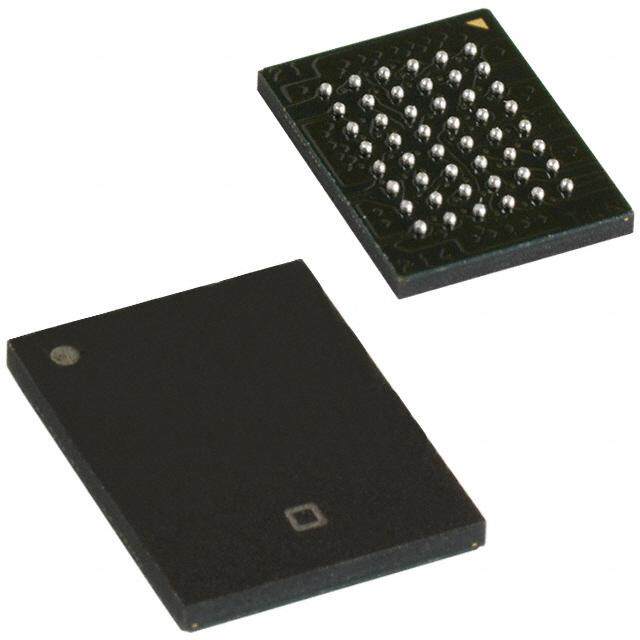
| 封装/外壳 | 28-SOIC(0.295",7.50mm 宽) |
| 封装/箱体 | SOIC-28 Wide |
| 工作温度 | -40°C ~ 85°C |
| 工厂包装数量 | 27 |
| 接口 | SPI |
| 支持标准 | 802.3 |
| 数据速率 | 10 Mb/s |
| 最大工作温度 | + 85 C |
| 最大电源电流 | 180 mA |
| 最小工作温度 | - 40 C |
| 标准 | 10 Base-T PHY |
| 标准包装 | 27 |
| 电压-电源 | 3.1 V ~ 3.6 V |
| 电流-电源 | 160mA |
| 配用 | /product-detail/zh/DM163024/DM163024-ND/1245284/product-detail/zh/AC164123/AC164123-ND/1212492/product-detail/zh/AC164121/AC164121-ND/807377 |


- 商务部:美国ITC正式对集成电路等产品启动337调查
- 曝三星4nm工艺存在良率问题 高通将骁龙8 Gen1或转产台积电
- 太阳诱电将投资9.5亿元在常州建新厂生产MLCC 预计2023年完工
- 英特尔发布欧洲新工厂建设计划 深化IDM 2.0 战略
- 台积电先进制程称霸业界 有大客户加持明年业绩稳了
- 达到5530亿美元!SIA预计今年全球半导体销售额将创下新高
- 英特尔拟将自动驾驶子公司Mobileye上市 估值或超500亿美元
- 三星加码芯片和SET,合并消费电子和移动部门,撤换高东真等 CEO
- 三星电子宣布重大人事变动 还合并消费电子和移动部门
- 海关总署:前11个月进口集成电路产品价值2.52万亿元 增长14.8%


PDF Datasheet 数据手册内容提取
ENC28J60 Data Sheet Stand-Alone Ethernet Controller with SPI Interface Preliminary © 2006 Microchip Technology Inc. DS39662B
Note the following details of the code protection feature on Microchip devices: (cid:129) Microchip products meet the specification contained in their particular Microchip Data Sheet. (cid:129) Microchip believes that its family of products is one of the most secure families of its kind on the market today, when used in the intended manner and under normal conditions. (cid:129) There are dishonest and possibly illegal methods used to breach the code protection feature. All of these methods, to our knowledge, require using the Microchip products in a manner outside the operating specifications contained in Microchip’s Data Sheets. Most likely, the person doing so is engaged in theft of intellectual property. (cid:129) Microchip is willing to work with the customer who is concerned about the integrity of their code. (cid:129) Neither Microchip nor any other semiconductor manufacturer can guarantee the security of their code. Code protection does not mean that we are guaranteeing the product as “unbreakable.” Code protection is constantly evolving. We at Microchip are committed to continuously improving the code protection features of our products. Attempts to break Microchip’s code protection feature may be a violation of the Digital Millennium Copyright Act. If such acts allow unauthorized access to your software or other copyrighted work, you may have a right to sue for relief under that Act. Information contained in this publication regarding device Trademarks applications and the like is provided only for your convenience The Microchip name and logo, the Microchip logo, Accuron, and may be superseded by updates. It is your responsibility to dsPIC, KEELOQ, microID, MPLAB, PIC, PICmicro, PICSTART, ensure that your application meets with your specifications. PROMATE, PowerSmart, rfPIC and SmartShunt are MICROCHIP MAKES NO REPRESENTATIONS OR registered trademarks of Microchip Technology Incorporated WARRANTIES OF ANY KIND WHETHER EXPRESS OR in the U.S.A. and other countries. IMPLIED, WRITTEN OR ORAL, STATUTORY OR OTHERWISE, RELATED TO THE INFORMATION, AmpLab, FilterLab, Migratable Memory, MXDEV, MXLAB, INCLUDING BUT NOT LIMITED TO ITS CONDITION, SEEVAL, SmartSensor and The Embedded Control Solutions QUALITY, PERFORMANCE, MERCHANTABILITY OR Company are registered trademarks of Microchip Technology FITNESS FOR PURPOSE. Microchip disclaims all liability Incorporated in the U.S.A. arising from this information and its use. Use of Microchip Analog-for-the-Digital Age, Application Maestro, CodeGuard, devices in life support and/or safety applications is entirely at dsPICDEM, dsPICDEM.net, dsPICworks, ECAN, the buyer’s risk, and the buyer agrees to defend, indemnify and ECONOMONITOR, FanSense, FlexROM, fuzzyLAB, hold harmless Microchip from any and all damages, claims, In-Circuit Serial Programming, ICSP, ICEPIC, Linear Active suits, or expenses resulting from such use. No licenses are Thermistor, Mindi, MiWi, MPASM, MPLIB, MPLINK, PICkit, conveyed, implicitly or otherwise, under any Microchip PICDEM, PICDEM.net, PICLAB, PICtail, PowerCal, intellectual property rights. PowerInfo, PowerMate, PowerTool, REAL ICE, rfLAB, rfPICDEM, Select Mode, Smart Serial, SmartTel, Total Endurance, UNI/O, WiperLock and ZENA are trademarks of Microchip Technology Incorporated in the U.S.A. and other countries. SQTP is a service mark of Microchip Technology Incorporated in the U.S.A. All other trademarks mentioned herein are property of their respective companies. © 2006, Microchip Technology Incorporated, Printed in the U.S.A., All Rights Reserved. Printed on recycled paper. Microchip received ISO/TS-16949:2002 certification for its worldwide headquarters, design and wafer fabrication facilities in Chandler and Tempe, Arizona, Gresham, Oregon and Mountain View, California. The Company’s quality system processes and procedures are for its PICmicro® 8-bit MCUs, KEELOQ® code hopping devices, Serial EEPROMs, microperipherals, nonvolatile memory and analog products. In addition, Microchip’s quality system for the design and manufacture of development systems is ISO 9001:2000 certified. Preliminary DS39662B-page ii © 2006 Microchip Technology Inc.
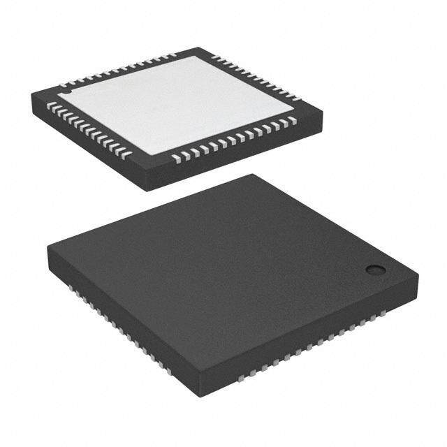
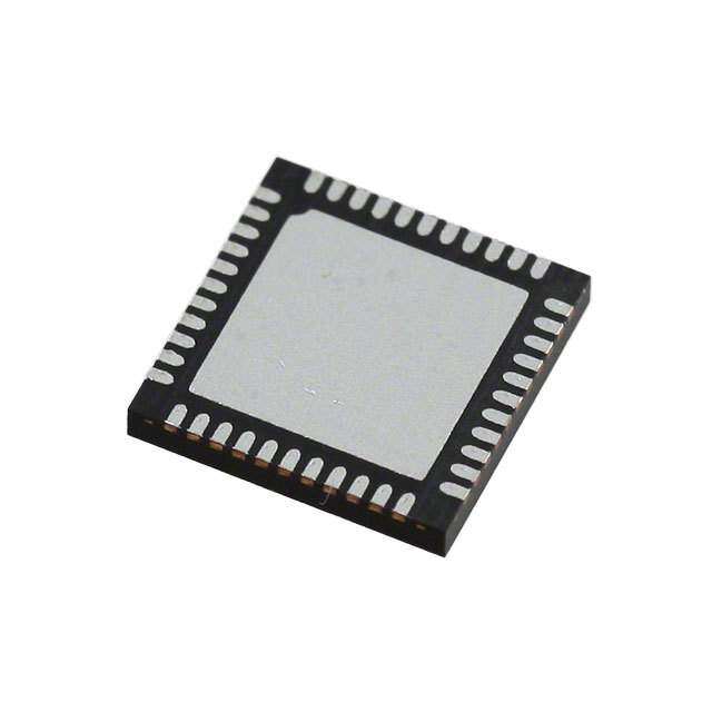
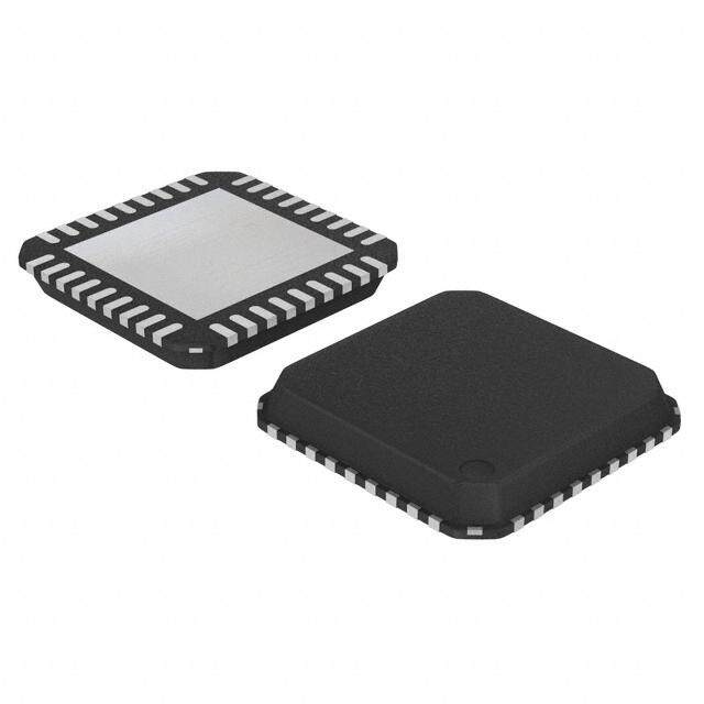
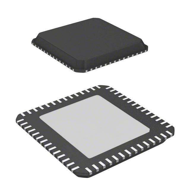
ENC28J60 Stand-Alone Ethernet Controller with SPI Interface Ethernet Controller Features Operational (cid:129) IEEE 802.3 compatible Ethernet controller (cid:129) Six interrupt sources and one interrupt output pin (cid:129) Integrated MAC and 10BASE-T PHY (cid:129) 25MHz clock input requirement (cid:129) Supports one 10BASE-T port with automatic (cid:129) Clock out pin with programmable prescaler polarity detection and correction (cid:129) Operating voltage of 3.1V to 3.6V (3.3V typical) (cid:129) Supports Full and Half-Duplex modes (cid:129) 5V tolerant inputs (cid:129) Programmable automatic retransmit on collision (cid:129) Temperature range: -40°C to +85°C Industrial, (cid:129) Programmable padding and CRC generation 0°C to +70°C Commercial (SSOP only) (cid:129) Programmable automatic rejection of erroneous (cid:129) 28-pin SPDIP, SSOP, SOIC, QFN packages packets (cid:129) SPI Interface with clock speeds up to 20MHz Package Types 28-Pin SPDIP, SSOP, SOIC Buffer (cid:129) 8-Kbyte transmit/receive packet dual port SRAM VCAP 1 28 VDD VSS 2 27 LEDA (cid:129) Configurable transmit/receive buffer size CLKOUT 3 26 LEDB (cid:129) Hardware-managed circular receive FIFO INT 4 25 VDDOSC NC* 5 E 24 OSC2 (cid:129) Byte-wide random and sequential access with SO 6 NC 23 OSC1 auto-increment SI 7 2 22 VSSOSC (cid:129) Internal DMA for fast data movement SCK 8 8J 21 VSSPLL CS 9 60 20 VDDPLL (cid:129) Hardware assisted checksum calculation for vari- RESET 10 19 VDDRX ous network protocols VSSRX 11 18 VSSTX TPIN- 12 17 TPOUT+ Medium Access Controller (MAC) TPIN+ 13 16 TPOUT- RBIAS 14 15 VDDTX Features (cid:129) Supports Unicast, Multicast and Broadcast (cid:129) pParocgkeratsmmable receive packet filtering and 28-pin QFN INTCLKOUTVSSVCAPVDD LEDALEDB wake-up host on logical AND or OR of the following: - Unicast destination address 28272625242322 - Multicast address NC* 1 21 VDDOSC - Broadcast address SO 2 20 OSC2 - Magic Packet™ SI 3 19 OSC1 SCK 4 ENC28J60 18 VSSOSC - Group destination addresses as defined by CS 5 17 VSSPLL 64-bit hash table RESET 6 16 VDDPLL - Programmable pattern matching of up to VSSRX 7 15 VDDRX 64 bytes at user-defined offset 8 91011121314 Physical Layer (PHY) Features (cid:129)(cid:129) LTowoop pbraocgkr ammomdeable LED outputs for LINK, TX, TPIN- TPIN+ RBIASVDDTX TPOUT-TPOUT+VSSTX RX, collision and full/half-duplex status * Reserved pin; always leave disconnected. Preliminary © 2006 Microchip Technology Inc. DS39662B-page 1
ENC28J60 Table of Contents 1.0 Overview......................................................................................................................................................................................3 2.0 External Connections...................................................................................................................................................................5 3.0 Memory Organization.................................................................................................................................................................11 4.0 Serial Peripheral Interface (SPI).................................................................................................................................................25 5.0 Ethernet Overview......................................................................................................................................................................31 6.0 Initialization.................................................................................................................................................................................33 7.0 Transmitting and Receiving Packets..........................................................................................................................................39 8.0 Receive Filters............................................................................................................................................................................47 9.0 Duplex Mode Configuration and Negotiation..............................................................................................................................53 10.0 Flow Control...............................................................................................................................................................................55 11.0 Reset..........................................................................................................................................................................................59 12.0 Interrupts....................................................................................................................................................................................63 13.0 Direct Memory Access Controller...............................................................................................................................................71 14.0 Power-Down...............................................................................................................................................................................73 15.0 Built-in Self-Test Controller........................................................................................................................................................75 16.0 Electrical Characteristics............................................................................................................................................................79 17.0 Packaging Information................................................................................................................................................................83 Index....................................................................................................................................................................................................89 The Microchip Web Site.......................................................................................................................................................................91 Customer Change Notification Service................................................................................................................................................91 Customer Support................................................................................................................................................................................91 Reader Response................................................................................................................................................................................92 Product Identification System...............................................................................................................................................................93 TO OUR VALUED CUSTOMERS It is our intention to provide our valued customers with the best documentation possible to ensure successful use of your Microchip products. To this end, we will continue to improve our publications to better suit your needs. Our publications will be refined and enhanced as new volumes and updates are introduced. If you have any questions or comments regarding this publication, please contact the Marketing Communications Department via E-mail at docerrors@microchip.com or fax the Reader Response Form in the back of this data sheet to (480) 792-4150. We welcome your feedback. Most Current Data Sheet To obtain the most up-to-date version of this data sheet, please register at our Worldwide Web site at: http://www.microchip.com You can determine the version of a data sheet by examining its literature number found on the bottom outside corner of any page. The last character of the literature number is the version number, (e.g., DS30000A is version A of document DS30000). Errata An errata sheet, describing minor operational differences from the data sheet and recommended workarounds, may exist for current devices. As device/documentation issues become known to us, we will publish an errata sheet. The errata will specify the revision of silicon and revision of document to which it applies. To determine if an errata sheet exists for a particular device, please check with one of the following: (cid:129) Microchip’s Worldwide Web site; http://www.microchip.com (cid:129) Your local Microchip sales office (see last page) When contacting a sales office, please specify which device, revision of silicon and data sheet (include literature number) you are using. Customer Notification System Register on our web site at www.microchip.com to receive the most current information on all of our products. Preliminary DS39662B-page 2 © 2006 Microchip Technology Inc.
ENC28J60 1.0 OVERVIEW The ENC28J60 consists of seven major functional blocks: The ENC28J60 is a stand-alone Ethernet controller 1. An SPI interface that serves as a communica- with an industry standard Serial Peripheral Interface tion channel between the host controller and the (SPI). It is designed to serve as an Ethernet network ENC28J60. interface for any controller equipped with SPI. 2. Control Registers which are used to control and The ENC28J60 meets all of the IEEE 802.3 specifica- monitor the ENC28J60. tions. It incorporates a number of packet filtering 3. A dual port RAM buffer for received and schemes to limit incoming packets. It also provides an transmitted data packets. internal DMA module for fast data throughput and hard- ware assisted checksum calculation, which is used in 4. An arbiter to control the access to the RAM various network protocols. Communication with the buffer when requests are made from DMA, host controller is implemented via an interrupt pin and transmit and receive blocks. the SPI, with clock rates of up to 20MHz. Two dedi- 5. The bus interface that interprets data and cated pins are used for LED link and network activity commands received via the SPI interface. indication. 6. The MAC (Medium Access Control) module that A simple block diagram of the ENC28J60 is shown in implements IEEE 802.3 compliant MAC logic. Figure1-1. A typical application circuit using the device 7. The PHY (Physical Layer) module that encodes is shown in Figure1-2. With the ENC28J60, two pulse and decodes the analog data that is present on transformers and a few passive components are all that the twisted pair interface. is required to connect a microcontroller to an Ethernet The device also contains other support blocks, such as network. the oscillator, on-chip voltage regulator, level translators to provide 5V tolerant I/Os and system control logic. FIGURE 1-1: ENC28J60 BLOCK DIAGRAM LEDA Buffer RX LEDB 8 Kbytes Dual Port RAM MAC RXBM TPOUT+ RXF (Filter) MII TX TPOUT- ch0 Interface CLKOUT DMA & Control Arbiter ch0 Checksum Registers PHY TPIN+ ch1 TX ch1 RX TPIN- TXBM INT Flow Control Bus Interface MIIM RBIAS Interface Host Interface CS(1) SI(1) OSC1 SO SPI System Control PoRweesre-ton RVeoglutalagteor O2s5c iMllaHtzor OSC2 SCK(1) RESET(1) VCAP Note1: These pins are 5V tolerant. Preliminary © 2006 Microchip Technology Inc. DS39662B-page 3
ENC28J60 FIGURE 1-2: TYPICAL ENC28J60-BASED INTERFACE MCU ENC28J60 TPIN+/- CS RJ45 I/O SI TPOUT+/- SDO SO SDI ETHERNET SCK SCK TX/RX MAC PHY TRANSFORMER Buffer INT LEDA INTX LEDB TABLE 1-1: PINOUT I/O DESCRIPTIONS Pin Number Pin Buffer Pin Name SPDIP, QFN Type Type Description SOIC, SSOP VCAP 1 25 P — 2.5V output from internal regulator. A low Equivalent Series Resistance (ESR) capacitor, with a typical value of 10 μF and a minimum value of 1μF to ground, must be placed on this pin. VSS 2 26 P — Ground reference. CLKOUT 3 27 O — Programmable clock output pin.(1) INT 4 28 O — INT interrupt output pin.(2) NC 5 1 O — Reserved function; always leave unconnected. SO 6 2 O — Data out pin for SPI interface.(2) SI 7 3 I ST Data in pin for SPI interface.(3) SCK 8 4 I ST Clock in pin for SPI interface.(3) CS 9 5 I ST Chip select input pin for SPI interface.(3,4) RESET 10 6 I ST Active-low device Reset input.(3, 4) VSSRX 11 7 P — Ground reference for PHY RX. TPIN- 12 8 I ANA Differential signal input. TPIN+ 13 9 I ANA Differential signal input. RBIAS 14 10 I ANA Bias current pin for PHY. Must be tied to ground via a resistor (refer to Section2.4 “Magnetics, Termination and Other External Components” for details). VDDTX 15 11 P — Positive supply for PHY TX. TPOUT- 16 12 O — Differential signal output. TPOUT+ 17 13 O — Differential signal output. VSSTX 18 14 P — Ground reference for PHY TX. VDDRX 19 15 P — Positive 3.3V supply for PHY RX. VDDPLL 20 16 P — Positive 3.3V supply for PHY PLL. VSSPLL 21 17 P — Ground reference for PHY PLL. VSSOSC 22 18 P — Ground reference for oscillator. OSC1 23 19 I ANA Oscillator input. OSC2 24 20 O — Oscillator output. VDDOSC 25 21 P — Positive 3.3V supply for oscillator. LEDB 26 22 O — LEDB driver pin.(5) LEDA 27 23 O — LEDA driver pin.(5) VDD 28 24 P — Positive 3.3V supply. Legend: I = Input, O = Output, P = Power, DIG = Digital input, ANA = Analog signal input, ST = Schmitt Trigger Note 1: Pins have a maximum current capacity of 8mA. 2: Pins have a maximum current capacity of 4mA. 3: Pins are 5V tolerant. 4: Pins have an internal weak pull-up to VDD. 5: Pins have a maximum current capacity of 12mA. Preliminary DS39662B-page 4 © 2006 Microchip Technology Inc.
ENC28J60 2.0 EXTERNAL CONNECTIONS 2.2 Oscillator Start-up Timer The ENC28J60 contains an Oscillator Start-up Timer 2.1 Oscillator (OST) to ensure that the oscillator and integrated PHY have stabilized before use. The OST does not expire The ENC28J60 is designed to operate at 25MHz with until 7500 OSC1 clock cycles (300μs) pass after a crystal connected to the OSC1 and OSC2 pins. The Power-on Reset or wake-up from Power-Down mode ENC28J60 design requires the use of a parallel cut occurs. During the delay, all Ethernet registers and crystal. Use of a series cut crystal may give a frequency buffer memory may still be read and written to through out of the crystal manufacturer specifications. A typical the SPI bus. However, software should not attempt to oscillator circuit is shown in Figure2-1. transmit any packets (set ECON1.TXRTS), enable The ENC28J60 may also be driven by an external clock reception of packets (set ECON1.RXEN) or access any source connected to the OSC1 pin as shown in MAC, MII or PHY registers during this period. Figure2-2. When the OST expires, the CLKRDY bit in the ESTAT register will be set. The application software should poll FIGURE 2-1: CRYSTAL OSCILLATOR this bit as necessary to determine when normal device OPERATION operation can begin. ENC28J60 Note: After a Power-on Reset, or the ENC28J60 is removed from Power-Down mode, the OSC1 CLKRDY bit must be polled before C1 To Internal Logic transmitting packets, enabling packet reception or accessing any MAC, MII or XTAL PHY registers. RF(2) RS(1) C2 OSC2 Note 1: A series resistor, RS, may be required for AT strip cut crystals. 2: The feedback resistor, RF, is typically in the range of 2 to 10MΩ. FIGURE 2-2: EXTERNAL CLOCK SOURCE(1) ENC28J60 3.3V Clock from OSC1 External System Open(2) OSC2 Note 1: Duty cycle restrictions must be observed. 2: A resistor to ground may be used to reduce system noise. This may increase system current. Preliminary © 2006 Microchip Technology Inc. DS39662B-page 5
ENC28J60 2.3 CLKOUT Pin value). Additionally, Power-Down mode may be entered and the CLKOUT function will continue to The clock out pin is provided to the system designer for operate. When Power-Down mode is cancelled, the use as the host controller clock or as a clock source for OST will be reset but the CLKOUT function will other devices in the system. The CLKOUT has an continue. When the CLKOUT function is disabled internal prescaler which can divide the output by 1, 2, (ECOCON = 0), the CLKOUT pin is driven low. 3, 4 or 8. The CLKOUT function is enabled and the The CLKOUT function is designed to ensure that mini- prescaler is selected via the ECOCON register mum timings are preserved when the CLKOUT pin (Register2-1). function is enabled, disabled or the prescaler value is To create a clean clock signal, the CLKOUT pin is held changed. No high or low pulses will be outputted which low for a period when power is first applied. After the exceed the frequency specified by the ECOCON Power-on Reset ends, the OST will begin counting. configuration. However, when switching frequencies, a When the OST expires, the CLKOUT pin will begin out- delay between two and eight OSC1 clock periods will putting its default frequency of 6.25MHz (main clock occur where no clock pulses will be produced (see divided by 4). At any future time that the ENC28J60 is Figure2-3). During this period, CLKOUT will be held reset by software or the RESET pin, the CLKOUT func- low. tion will not be altered (ECOCON will not change FIGURE 2-3: CLKOUT TRANSITION ECOCON 80 ns to 320 ns Delay Changed REGISTER 2-1: ECOCON: CLOCK OUTPUT CONTROL REGISTER U-0 U-0 U-0 U-0 U-0 R/W-1 R/W-0 R/W-0 — — — — — COCON2 COCON1 COCON0 bit 7 bit 0 Legend: R = Readable bit W = Writable bit U = Unimplemented bit, read as ‘0’ -n = Value at POR ‘1’ = Bit is set ‘0’ = Bit is cleared x = Bit is unknown bit 7-3 Unimplemented: Read as ‘0’ bit 2-0 COCON2:COCON0: Clock Output Configuration bits 11x = Reserved for factory test. Do not use. Glitch prevention not assured. 101 = CLKOUT outputs main clock divided by 8 (3.125 MHz) 100 = CLKOUT outputs main clock divided by 4 (6.25 MHz) 011 = CLKOUT outputs main clock divided by 3 (8.333333 MHz) 010 = CLKOUT outputs main clock divided by 2 (12.5 MHz) 001 = CLKOUT outputs main clock divided by 1 (25 MHz) 000 = CLKOUT is disabled. The pin is driven low. Preliminary DS39662B-page 6 © 2006 Microchip Technology Inc.
ENC28J60 2.4 Magnetics, Termination and Other A common-mode choke on the TPOUT interface, External Components placed between the TPOUT pins and the Ethernet transformer (not shown), is not recommend. If a com- To complete the Ethernet interface, the ENC28J60 mon-mode choke is used to reduce EMI emissions, it requires several standard components to be installed should be placed between the Ethernet transformer externally. These components should be connected as and pins 1 and 2 of the RJ-45 connector. Many Ether- shown in Figure2-4. net transformer modules include common-mode The internal analog circuitry in the PHY module requires chokes inside the same device package. The trans- that an external 2.32 kΩ, 1% resistor be attached from formers should have at least the isolation rating speci- RBIAS to ground. The resistor influences the TPOUT+/- fied in Table16-5 to protect against static voltages and signal amplitude. The resistor should be placed as close meet IEEE 802.3 isolation requirements (see as possible to the chip with no immediately adjacent Section16.0 “Electrical Characteristics” for specific signal traces to prevent noise capacitively coupling into transformer requirements). Both transmit and receive the pin and affecting the transmit behavior. It is interfaces additionally require two resistors and a recommended that the resistor be a surface mount type. capacitor to properly terminate the transmission line, minimizing signal reflections. Some of the device’s digital logic operates at a nominal 2.5V. An on-chip voltage regulator is incorporated to All power supply pins must be externally connected to generate this voltage. The only external component the same power source. Similarly, all ground refer- required is an external filter capacitor, connected from ences must be externally connected to the same VCAP to ground. The capacitor must have low equiva- ground node. Each VDD and VSS pin pair should have lent-series resistance (ESR), with a typical value of a 0.1μF ceramic bypass capacitor (not shown in the 10μF, and a minimum value of 1μF. The internal regu- schematic) placed as close to the pins as possible. lator is not designed to drive external loads. Since relatively high currents are necessary to operate On the TPIN+/TPIN- and TPOUT+/TPOUT- pins, the twisted-pair interface, all wires should be kept as 1:1center-taped pulse transformers rated for Ethernet short as possible. Reasonable wire widths should be operations are required. When the Ethernet module is used on power wires to reduce resistive loss. If the enabled, current is continually sunk through both differential data lines cannot be kept short, they should TPOUT pins. When the PHY is actively transmitting, a be routed in such a way as to have a 100Ω character- differential voltage is created on the Ethernet cable by istic impedance. varying the relative current sunk by TPOUT+ compared to TPOUT-. FIGURE 2-4: ENC28J60 ETHERNET TERMINATION AND EXTERNAL CONNECTIONS 3.3V ENC28J60 RJ-45 MCU 1 TPOUT+ Ferrite 1 I/O CS 49.9Ω, 1% Bead(1,3) SCK SCK 2 SDO SI 49.9Ω, 1% 0.1 μF(3) SDI SO TPOUT- 1:1 CT 3 TPIN+ Level 4 49.9Ω, 1% Shift Logic(2) 5 49.9Ω, 1% 0.1 μF INT0 INT TPIN- 1:1 CT 6 RBIAS 7 VCAP LEDA LEDB 8 10μF 2.32 kΩ, 1% 75Ω(3)75Ω(3)75Ω(3)75Ω(3) 1 nF, 2 kV(3) Note 1: Ferrite Bead should be rated for at least 80mA. 2: Required only if the microcontroller is operating at 5V. See Section2.5 “I/O Levels” for more information. 3: These components are installed for EMI reduction purposes. Preliminary © 2006 Microchip Technology Inc. DS39662B-page 7
ENC28J60 2.5 I/O Levels 2.6 LED Configuration The ENC28J60 is a 3.3V part; however, it was The LEDA and LEDB pins support automatic polarity designed to be easily integrated into 5V systems. The detection on Reset. The LEDs can be connected such SPI CS, SCK and SI inputs, as well as the RESET pin, that the pin must source current to turn the LED on, or are all 5V tolerant. On the other hand, if the host alternately connected such that the pin must sink cur- controller is operated at 5V, it quite likely will not be rent to turn the LED on. Upon system Reset, the within specifications when its SPI and interrupt inputs ENC28J60 will detect how the LED is connected and are driven by the 3.3V CMOS outputs on the begin driving the LED to the default state configured by ENC28J60. A unidirectional level translator would be the PHLCON register. If the LED polarity is changed necessary. while the ENC28J60 is operating, the new polarity will not be detected until the next system Reset occurs. An economical 74HCT08 (quad AND gate), 74ACT125 (quad 3-state buffer) or many other 5V CMOS chips LEDB is unique in that the connection of the LED is with TTL level input buffers may be used to provide the automatically read on Reset and determines how to ini- necessary level shifting. The use of 3-state buffers tialize the PHCON1.PDPXMD bit. If the pin sources permits easy integration into systems which share the current to illuminate the LED, the bit is cleared on SPI bus with other devices. Figure2-5 and Figure2-6 Reset and the PHY defaults to half-duplex operation. If show example translation schemes. the pin sinks current to illuminate the LED, the bit is set on Reset and the PHY defaults to full-duplex operation. FIGURE 2-5: LEVEL SHIFTING USING Figure2-7 shows the two available options. If no LED AND GATES is attached to the LEDB pin, the PDPXMD bit will reset to an indeterminate value. MCU ENC28J60 FIGURE 2-7: LEDB POLARITY AND RESET CONFIGURATION I/O CS OPTIONS SCK SCK SO SI Full-Duplex Operation: +3.3V PDPXMD = 1 SI SO OSC1 CLKOUT LEDB INT0 INT Half-Duplex Operation: PDPXMD = 0 FIGURE 2-6: LEVEL SHIFTING USING LEDB 3-STATE BUFFERS MCU ENC28J60 I/O CS SCK SCK SO SI The LEDs can also be configured separately to control their operating polarity (on or off when active), blink rate SI SO and blink stretch interval. The options are controlled by the LACFG3:LACFG0 and LBCFG3:LBCFG0 bits. OSC1 CLKOUT Typical values for blink stretch are listed in Table2-1. INT0 INT TABLE 2-1: LED BLINK STRETCH LENGTH Stretch Length Typical Stretch (ms) TNSTRCH (normal) 40 TMSTRCH (medium) 70 TLSTRCH (long) 140 Preliminary DS39662B-page 8 © 2006 Microchip Technology Inc.
ENC28J60 REGISTER 2-2: PHLCON: PHY MODULE LED CONTROL REGISTER R/W-0 R/W-0 R/W-1 R/W-1 R/W-0 R/W-1 R/W-0 R/W-0 r r r r LACFG3 LACFG2 LACFG1 LACFG0 bit 15 bit 8 R/W-0 R/W-0 R/W-1 R/W-0 R/W-0 R/W-0 R/W-1 R/W-x LBCFG3 LBCFG2 LBCFG1 LBCFG0 LFRQ1 LFRQ0 STRCH r bit 7 bit 0 Legend: R = Readable bit W = Writable bit U = Unimplemented bit, read as ‘0’ -n = Value at POR ‘1’ = Bit is set ‘0’ = Bit is cleared x = Bit is unknown bit 15-14 Reserved: Write as ‘0’ bit 13-12 Reserved: Write as ‘1’ bit 11-8 LACFG3:LACFG0: LEDA Configuration bits 1111 = Reserved 1110 = Display duplex status and collision activity (always stretched) 1101 = Display link status and transmit/receive activity (always stretched) 1100 = Display link status and receive activity (always stretched) 1011 = Blink slow 1010 = Blink fast 1001 = Off 1000 = On 0111 = Display transmit and receive activity (stretchable) 0110 = Reserved 0101 = Display duplex status 0100 = Display link status 0011 = Display collision activity (stretchable) 0010 = Display receive activity (stretchable) 0001 = Display transmit activity (stretchable) 0000 = Reserved bit 7-4 LBCFG3:LBCFG0: LEDB Configuration bits 1110 = Display duplex status and collision activity (always stretched) 1101 = Display link status and transmit/receive activity (always stretched) 1100 = Display link status and receive activity (always stretched) 1011 = Blink slow 1010 = Blink fast 1001 = Off 1000 = On 0111 = Display transmit and receive activity (stretchable) 0110 = Reserved 0101 = Display duplex status 0100 = Display link status 0011 = Display collision activity (stretchable) 0010 = Display receive activity (stretchable) 0001 = Display transmit activity (stretchable) 0000 = Reserved bit 3-2 LFRQ1:LFRQ0: LED Pulse Stretch Time Configuration bits (see Table2-1) 11 = Reserved 10 = Stretch LED events by TLSTRCH 01 = Stretch LED events by TMSTRCH 00 = Stretch LED events by TNSTRCH bit 1 STRCH: LED Pulse Stretching Enable bit 1 = Stretchable LED events will cause lengthened LED pulses based on LFRQ1:LFRQ0 configuration 0 = Stretchable LED events will only be displayed while they are occurring bit 0 Reserved: Write as ‘0’ Preliminary © 2006 Microchip Technology Inc. DS39662B-page 9
ENC28J60 NOTES: Preliminary DS39662B-page 10 © 2006 Microchip Technology Inc.
ENC28J60 3.0 MEMORY ORGANIZATION The Ethernet buffer contains transmit and receive memory used by the Ethernet controller in a single All memory in the ENC28J60 is implemented as static memory space. The sizes of the memory areas are RAM. There are three types of memory in the programmable by the host controller using the SPI ENC28J60: interface. The Ethernet buffer memory can only be (cid:129) Control Registers accessed via the read buffer memory and write buffer memory SPI commands (see Section4.2.2 “Read (cid:129) Ethernet Buffer Buffer Memory Command” and Section4.2.4 “Write (cid:129) PHY Registers Buffer Memory Command”). The Control registers’ memory contains the registers The PHY registers are used for configuration, control that are used for configuration, control and status and status retrieval of the PHY module. The registers retrieval of the ENC28J60. The Control registers are are not directly accessible through the SPI interface; directly read and written to by the SPI interface. they can only be accessed through Media Independent Interface Management (MIIM) implemented in the MAC. Figure3-1 shows the data memory organization for the ENC28J60. FIGURE 3-1: ENC28J60 MEMORY ORGANIZATION ECON1<1:0> Control Registers Ethernet Buffer 00h 0000h Buffer Pointers in Bank 0 = 00 Bank 0 19h 1Ah Common 1Fh Registers 00h = 01 Bank 1 19h 1Ah Common 1Fh Registers 00h = 10 Bank 2 19h 1Ah Common 1FFFh 1Fh Registers 00h = 11 Bank 3 19h PHY Registers 1Ah Common 00h Registers 1Fh 1Fh Note: Memory areas are not shown to scale. The size of the control memory space has been scaled to show detail. Preliminary © 2006 Microchip Technology Inc. DS39662B-page 11
ENC28J60 3.1 Control Registers Some of the available addresses are unimplemented. Any attempts to write to these locations are ignored The Control Registers provide the main interface while reads return ‘0’s. The register at address 1Ah in between the host controller and the on-chip Ethernet each bank is reserved; read and write operations controller logic. Writing to these registers controls the should not be performed on this register. All other operation of the interface, while reading the registers reserved registers may be read, but their contents must allows the host controller to monitor operations. not be changed. When reading and writing to registers The Control Register memory is partitioned into four which contain reserved bits, any rules stated in the banks, selectable by the bank select bits register definition should be observed. BSEL1:BSEL0 in the ECON1 register. Each bank is Control registers for the ENC28J60 are generically 32bytes long and addressed by a 5-bit address value. grouped as ETH, MAC and MII registers. Register The last five locations (1Bh to 1Fh) of all banks point to a names starting with “E” belong to the ETH group. common set of registers: EIE, EIR, ESTAT, ECON2 and Similarly, registers names starting with “MA” belong to ECON1. These are key registers used in controlling and the MAC group and registers prefixed with “MI” belong monitoring the operation of the device. Their common to the MII group. mapping allows easy access without switching the bank. The ECON1 and ECON2 registers are discussed later in this section. TABLE 3-1: ENC28J60 CONTROL REGISTER MAP Bank 0 Bank 1 Bank 2 Bank 3 Address Name Address Name Address Name Address Name 00h ERDPTL 00h EHT0 00h MACON1 00h MAADR5 01h ERDPTH 01h EHT1 01h Reserved 01h MAADR6 02h EWRPTL 02h EHT2 02h MACON3 02h MAADR3 03h EWRPTH 03h EHT3 03h MACON4 03h MAADR4 04h ETXSTL 04h EHT4 04h MABBIPG 04h MAADR1 05h ETXSTH 05h EHT5 05h — 05h MAADR2 06h ETXNDL 06h EHT6 06h MAIPGL 06h EBSTSD 07h ETXNDH 07h EHT7 07h MAIPGH 07h EBSTCON 08h ERXSTL 08h EPMM0 08h MACLCON1 08h EBSTCSL 09h ERXSTH 09h EPMM1 09h MACLCON2 09h EBSTCSH 0Ah ERXNDL 0Ah EPMM2 0Ah MAMXFLL 0Ah MISTAT 0Bh ERXNDH 0Bh EPMM3 0Bh MAMXFLH 0Bh — 0Ch ERXRDPTL 0Ch EPMM4 0Ch Reserved 0Ch — 0Dh ERXRDPTH 0Dh EPMM5 0Dh Reserved 0Dh — 0Eh ERXWRPTL 0Eh EPMM6 0Eh Reserved 0Eh — 0Fh ERXWRPTH 0Fh EPMM7 0Fh — 0Fh — 10h EDMASTL 10h EPMCSL 10h Reserved 10h — 11h EDMASTH 11h EPMCSH 11h Reserved 11h — 12h EDMANDL 12h — 12h MICMD 12h EREVID 13h EDMANDH 13h — 13h — 13h — 14h EDMADSTL 14h EPMOL 14h MIREGADR 14h — 15h EDMADSTH 15h EPMOH 15h Reserved 15h ECOCON 16h EDMACSL 16h Reserved 16h MIWRL 16h Reserved 17h EDMACSH 17h Reserved 17h MIWRH 17h EFLOCON 18h — 18h ERXFCON 18h MIRDL 18h EPAUSL 19h — 19h EPKTCNT 19h MIRDH 19h EPAUSH 1Ah Reserved 1Ah Reserved 1Ah Reserved 1Ah Reserved 1Bh EIE 1Bh EIE 1Bh EIE 1Bh EIE 1Ch EIR 1Ch EIR 1Ch EIR 1Ch EIR 1Dh ESTAT 1Dh ESTAT 1Dh ESTAT 1Dh ESTAT 1Eh ECON2 1Eh ECON2 1Eh ECON2 1Eh ECON2 1Fh ECON1 1Fh ECON1 1Fh ECON1 1Fh ECON1 Preliminary DS39662B-page 12 © 2006 Microchip Technology Inc.
ENC28J60 TABLE 3-2: ENC28J60 CONTROL REGISTER SUMMARY Value Details Register Name Bit 7 Bit 6 Bit 5 Bit 4 Bit 3 Bit 2 Bit 1 Bit 0 on on Reset Page EIE INTIE PKTIE DMAIE LINKIE TXIE r TXERIE RXERIE 0000 0000 65 EIR — PKTIF DMAIF LINKIF TXIF r TXERIF RXERIF -000 0000 66 ESTAT INT BUFER r LATECOL — RXBUSY TXABRT CLKRDY(1) 0000 -000 64 ECON2 AUTOINC PKTDEC PWRSV r VRPS — — — 1000 0--- 16 ECON1 TXRST RXRST DMAST CSUMEN TXRTS RXEN BSEL1 BSEL0 0000 0000 15 ERDPTL Read Pointer Low Byte ERDPT<7:0>) 1111 1010 17 ERDPTH — — — Read Pointer High Byte (ERDPT<12:8>) ---0 0101 17 EWRPTL Write Pointer Low Byte (EWRPT<7:0>) 0000 0000 17 EWRPTH — — — Write Pointer High Byte (EWRPT<12:8>) ---0 0000 17 ETXSTL TX Start Low Byte (ETXST<7:0>) 0000 0000 17 ETXSTH — — — TX Start High Byte (ETXST<12:8>) ---0 0000 17 ETXNDL TX End Low Byte (ETXND<7:0>) 0000 0000 17 ETXNDH — — — TX End High Byte (ETXND<12:8>) ---0 0000 17 ERXSTL RX Start Low Byte (ERXST<7:0>) 1111 1010 17 ERXSTH — — — RX Start High Byte (ERXST<12:8>) ---0 0101 17 ERXNDL RX End Low Byte (ERXND<7:0>) 1111 1111 17 ERXNDH — — — RX End High Byte (ERXND<12:8>) ---1 1111 17 ERXRDPTL RX RD Pointer Low Byte (ERXRDPT<7:0>) 1111 1010 17 ERXRDPTH — — — RX RD Pointer High Byte (ERXRDPT<12:8>) ---0 0101 17 ERXWRPTL RX WR Pointer Low Byte (ERXWRPT<7:0>) 0000 0000 17 ERXWRPTH — — — RX WR Pointer High Byte (ERXWRPT<12:8>) ---0 0000 17 EDMASTL DMA Start Low Byte (EDMAST<7:0>) 0000 0000 71 EDMASTH — — — DMA Start High Byte (EDMAST<12:8>) ---0 0000 71 EDMANDL DMA End Low Byte (EDMAND<7:0>) 0000 0000 71 EDMANDH — — — DMA End High Byte (EDMAND<12:8>) ---0 0000 71 EDMADSTL DMA Destination Low Byte (EDMADST<7:0>) 0000 0000 71 EDMADSTH — — — DMA Destination High Byte (EDMADST<12:8>) ---0 0000 71 EDMACSL DMA Checksum Low Byte (EDMACS<7:0>) 0000 0000 72 EDMACSH DMA Checksum High Byte (EDMACS<15:8>) 0000 0000 72 EHT0 Hash Table Byte 0 (EHT<7:0>) 0000 0000 52 EHT1 Hash Table Byte 1 (EHT<15:8>) 0000 0000 52 EHT2 Hash Table Byte 2 (EHT<23:16>) 0000 0000 52 EHT3 Hash Table Byte 3 (EHT<31:24>) 0000 0000 52 EHT4 Hash Table Byte 4 (EHT<39:32>) 0000 0000 52 EHT5 Hash Table Byte 5 (EHT<47:40>) 0000 0000 52 EHT6 Hash Table Byte 6 (EHT<55:48>) 0000 0000 52 EHT7 Hash Table Byte 7 (EHT<63:56>) 0000 0000 52 EPMM0 Pattern Match Mask Byte 0 (EPMM<7:0>) 0000 0000 51 EPMM1 Pattern Match Mask Byte 1 (EPMM<15:8>) 0000 0000 51 EPMM2 Pattern Match Mask Byte 2 (EPMM<23:16>) 0000 0000 51 EPMM3 Pattern Match Mask Byte 3 (EPMM<31:24>) 0000 0000 51 EPMM4 Pattern Match Mask Byte 4 (EPMM<39:32>) 0000 0000 51 EPMM5 Pattern Match Mask Byte 5 (EPMM<47:40>) 0000 0000 51 EPMM6 Pattern Match Mask Byte 6 (EPMM<55:48>) 0000 0000 51 EPMM7 Pattern Match Mask Byte 7 (EPMM<63:56>) 0000 0000 51 Legend: x = unknown, u = unchanged, — = unimplemented, q = value depends on condition, r = reserved, do not modify. Note 1: CLKRDY resets to ‘0’ on Power-on Reset but is unaffected on all other Resets. 2: EREVID is a read-only register. 3: ECOCON resets to ‘---- -100’ on Power-on Reset and ‘---- -uuu’ on all other Resets. Preliminary © 2006 Microchip Technology Inc. DS39662B-page 13
ENC28J60 TABLE 3-2: ENC28J60 CONTROL REGISTER SUMMARY (CONTINUED) Value Details Register Name Bit 7 Bit 6 Bit 5 Bit 4 Bit 3 Bit 2 Bit 1 Bit 0 on on Reset Page EPMCSL Pattern Match Checksum Low Byte (EPMCS<7:0>) 0000 0000 51 EPMCSH Pattern Match Checksum High Byte (EPMCS<15:0>) 0000 0000 51 EPMOL Pattern Match Offset Low Byte (EPMO<7:0>) 0000 0000 51 EPMOH — — — Pattern Match Offset High Byte (EPMO<12:8>) ---0 0000 51 ERXFCON UCEN ANDOR CRCEN PMEN MPEN HTEN MCEN BCEN 1010 0001 48 EPKTCNT Ethernet Packet Count 0000 0000 43 MACON1 — — — r TXPAUS RXPAUS PASSALL MARXEN ---0 0000 34 MACON3 PADCFG2 PADCFG1 PADCFG0 TXCRCEN PHDREN HFRMEN FRMLNEN FULDPX 0000 0000 35 MACON4 — DEFER BPEN NOBKOFF — — r r -000 --00 36 MABBIPG — Back-to-Back Inter-Packet Gap (BBIPG<6:0>) -000 0000 36 MAIPGL — Non-Back-to-Back Inter-Packet Gap Low Byte (MAIPGL<6:0>) -000 0000 34 MAIPGH — Non-Back-to-Back Inter-Packet Gap High Byte (MAIPGH<6:0>) -000 0000 34 MACLCON1 — — — — Retransmission Maximum (RETMAX<3:0>) ---- 1111 34 MACLCON2 — — Collision Window (COLWIN<5:0>) --11 0111 34 MAMXFLL Maximum Frame Length Low Byte (MAMXFL<7:0>) 0000 0000 34 MAMXFLH Maximum Frame Length High Byte (MAMXFL<15:8>) 0000 0110 34 MICMD — — — — — — MIISCAN MIIRD ---- --00 21 MIREGADR — — — MII Register Address (MIREGADR<4:0>) ---0 0000 19 MIWRL MII Write Data Low Byte (MIWR<7:0>) 0000 0000 19 MIWRH MII Write Data High Byte (MIWR<15:8>) 0000 0000 19 MIRDL MII Read Data Low Byte (MIRD<7:0>) 0000 0000 19 MIRDH MII Read Data High Byte(MIRD<15:8>) 0000 0000 19 MAADR5 MAC Address Byte 5 (MAADR<15:8>) 0000 0000 34 MAADR6 MAC Address Byte 6 (MAADR<7:0>) 0000 0000 34 MAADR3 MAC Address Byte 3 (MAADR<31:24>), OUI Byte 3 0000 0000 34 MAADR4 MAC Address Byte 4 (MAADR<23:16>) 0000 0000 34 MAADR1 MAC Address Byte 1 (MAADR<47:40>), OUI Byte 1 0000 0000 34 MAADR2 MAC Address Byte 2 (MAADR<39:32>), OUI Byte 2 0000 0000 34 EBSTSD Built-in Self-Test Fill Seed (EBSTSD<7:0>) 0000 0000 76 EBSTCON PSV2 PSV1 PSV0 PSEL TMSEL1 TMSEL0 TME BISTST 0000 0000 75 EBSTCSL Built-in Self-Test Checksum Low Byte (EBSTCS<7:0>) 0000 0000 76 EBSTCSH Built-in Self-Test Checksum High Byte (EBSTCS<15:8>) 0000 0000 76 MISTAT — — — — r NVALID SCAN BUSY ---- 0000 21 EREVID(2) — — — Ethernet Revision ID (EREVID<4:0>) ---q qqqq 22 ECOCON(3) — — — — — COCON2 COCON1 COCON0 ---- -100 6 EFLOCON — — — — — FULDPXS FCEN1 FCEN0 ---- -000 56 EPAUSL Pause Timer Value Low Byte (EPAUS<7:0>) 0000 0000 57 EPAUSH Pause Timer Value High Byte (EPAUS<15:8>) 0001 0000 57 Legend: x = unknown, u = unchanged, — = unimplemented, q = value depends on condition, r = reserved, do not modify. Note 1: CLKRDY resets to ‘0’ on Power-on Reset but is unaffected on all other Resets. 2: EREVID is a read-only register. 3: ECOCON resets to ‘---- -100’ on Power-on Reset and ‘---- -uuu’ on all other Resets. Preliminary DS39662B-page 14 © 2006 Microchip Technology Inc.
ENC28J60 3.1.1 ECON1 REGISTER The ECON1 register, shown in Register3-1, is used to control the main functions of the ENC28J60. Receive enable, transmit request, DMA control and bank select bits can all be found in ECON1. REGISTER 3-1: ECON1: ETHERNET CONTROL REGISTER 1 R/W-0 R/W-0 R/W-0 R/W-0 R/W-0 R/W-0 R/W-0 R/W-0 TXRST RXRST DMAST CSUMEN TXRTS RXEN BSEL1 BSEL0 bit 7 bit 0 Legend: R = Readable bit W = Writable bit U = Unimplemented bit, read as ‘0’ -n = Value at POR ‘1’ = Bit is set ‘0’ = Bit is cleared x = Bit is unknown bit 7 TXRST: Transmit Logic Reset bit 1 = Transmit logic is held in Reset 0 = Normal operation bit 6 RXRST: Receive Logic Reset bit 1 = Receive logic is held in Reset 0 = Normal operations bit 5 DMAST: DMA Start and Busy Status bit 1 = DMA copy or checksum operation is in progress 0 = DMA hardware is Idle bit 4 CSUMEN: DMA Checksum Enable bit 1 = DMA hardware calculates checksums 0 = DMA hardware copies buffer memory bit 3 TXRTS: Transmit Request to Send bit 1 = The transmit logic is attempting to transmit a packet 0 = The transmit logic is Idle bit 2 RXEN: Receive Enable bit 1 = Packets which pass the current filter configuration will be written into the receive buffer 0 = All packets received will be ignored bit 1-0 BSEL1:BSEL0: Bank Select bits 11 = SPI accesses registers in Bank 3 10 = SPI accesses registers in Bank 2 01 = SPI accesses registers in Bank 1 00 = SPI accesses registers in Bank 0 Preliminary © 2006 Microchip Technology Inc. DS39662B-page 15
ENC28J60 3.1.2 ECON2 REGISTER The ECON2 register, shown in Register3-2, is used to control other main functions of the ENC28J60. REGISTER 3-2: ECON2: ETHERNET CONTROL REGISTER 2 R/W-1 R/W-0(1) R/W-0 R/W-0 R/W-0 U-0 U-0 U-0 AUTOINC PKTDEC PWRSV r VRPS — — — bit 7 bit 0 Legend: R = Readable bit W = Writable bit U = Unimplemented bit, read as ‘0’ -n = Value at POR ‘1’ = Bit is set ‘0’ = Bit is cleared x = Bit is unknown bit 7 AUTOINC: Automatic Buffer Pointer Increment Enable bit 1 = Automatically increment ERDPT or EWRPT on reading from or writing to EDATA 0 = Do not automatically change ERDPT and EWRPT after the buffer is accessed bit 6 PKTDEC: Packet Decrement bit 1 = Decrement the EPKTCNT register by one 0 = Leave EPKTCNT unchanged bit 5 PWRSV: Power Save Enable bit 1 = MAC, PHY and control logic are in Low-Power Sleep mode 0 = Normal operation bit 4 Reserved: Maintain as ‘0’ bit 3 VRPS: Voltage Regulator Power Save Enable bit When PWRSV = 1: 1 = Internal voltage regulator is in Low-Current mode 0 = Internal voltage regulator is in Normal Current mode When PWRSV = 0: The bit is ignored; the regulator always outputs as much current as the device requires. bit 2-0 Unimplemented: Read as ‘0’ Note 1: This bit is automatically cleared once it is set. Preliminary DS39662B-page 16 © 2006 Microchip Technology Inc.
ENC28J60 3.2 Ethernet Buffer 3.2.2 TRANSMIT BUFFER The Ethernet buffer contains transmit and receive Any space within the 8-Kbyte memory, which is not memory used by the Ethernet controller. The entire programmed as part of the receive FIFO buffer, is buffer is 8Kbytes, divided into separate receive and considered to be the transmit buffer. The responsibility transmit buffer spaces. The sizes and locations of of managing where packets are located in the transmit transmit and receive memory are fully programmable buffer belongs to the host controller. Whenever the host by the host controller using the SPI interface. controller decides to transmit a packet, the ETXST and ETXND Pointers are programmed with addresses The relationship of the buffer spaces is shown in specifying where, within the transmit buffer, the partic- Figure3-2. ular packet to transmit is located. The hardware does not check that the start and end addresses do not 3.2.1 RECEIVE BUFFER overlap with the receive buffer. To prevent buffer The receive buffer constitutes a circular FIFO buffer corruption, the host controller must make sure to not managed by hardware. The register pairs transmit a packet while the ETXST and ETXND ERXSTH:ERXSTL and ERXNDH:ERXNDL serve as Pointers are overlapping the receive buffer, or while the Pointers to define the buffer’s size and location within ETXND Pointer is too close to the receive buffer. See the memory. The byte pointed to by ERXST and the Section7.1 “Transmitting Packets” for more byte pointed to by ERXND are both included in the information. FIFO buffer. 3.2.3 READING AND WRITING TO As bytes of data are received from the Ethernet THE BUFFER interface, they are written into the receive buffer sequentially. However, after the memory pointed to by The Ethernet buffer contents are accessed from the ERXND is written to, the hardware will automatically host controller though separate Read and Write Point- write the next byte of received data to the memory ers (ERDPT and EWRPT) combined with the read pointed to by ERXST. As a result, the receive hardware buffer memory and write buffer memory SPI will never write outside the boundaries of the FIFO. commands. While sequentially reading from the receive buffer, a wrapping condition will occur at the The host controller may program the ERXST and end of the receive buffer. While sequentially writing to ERXND Pointers when the receive logic is not enabled. the buffer, no wrapping conditions will occur. See The Pointers must not be modified while the receive Section4.2.2 “Read Buffer Memory Command” and logic is enabled (ECON1.RXEN is set). If desired, the Section4.2.4 “Write Buffer Memory Command” for Pointers may span the 1FFFh to 0000h memory more information. boundary; the hardware will still operate as a FIFO. The ERXWRPTH:ERXWRPTL registers define a 3.2.4 DMA ACCESS TO THE BUFFER location within the FIFO where the hardware will write The integrated DMA controller must read from the buffer bytes that it receives. The Pointer is read-only and is when calculating a checksum and it must read and write automatically updated by the hardware whenever a to the buffer when copying memory. The DMA follows new packet is successfully received. The Pointer is the same wrapping rules that SPI accesses do. While it useful for determining how much free space is sequentially reads, it will be subject to a wrapping condi- available within the FIFO. tion at the end of the receive buffer. All writes it does will The ERXRDPT registers define a location within the not be subject to any wrapping conditions. See FIFO where the receive hardware is forbidden to write Section13.0 “Direct Memory Access Controller” for to. In normal operation, the receive hardware will write more information. data up to, but not including, the memory pointed to by ERXRDPT. If the FIFO fills up with data and new data continues to arrive, the hardware will not overwrite the previously received data. Instead, the new data will be thrown away and the old data will be preserved. In order to continuously receive new data, the host con- troller must periodically advance this Pointer whenever it finishes processing some, or all, of the old received data. Preliminary © 2006 Microchip Technology Inc. DS39662B-page 17
ENC28J60 FIGURE 3-2: ETHERNET BUFFER ORGANIZATION Transmit Buffer Start 0000h (ETXSTH:ETXSTL) Buffer Write Pointer Transmit Buffer Data (EWRPTH:EWRPTL) AAh (WBM AAh) Transmit Buffer Transmit Buffer End (ETXNDH:ETXNDL) Receive Buffer Start (ERXSTH:ERXSTL) Receive Buffer (Circular FIFO) Buffer Read Pointer Receive Buffer Data (ERDPTH:ERDPTL) 55h (RBM 55h) Receive Buffer End 1FFFh (ERXNDH:ERXNDL) Preliminary DS39662B-page 18 © 2006 Microchip Technology Inc.
ENC28J60 3.3 PHY Registers To write to a PHY register: 1. Write the address of the PHY register to write to The PHY registers provide configuration and control of into the MIREGADR register. the PHY module, as well as status information about its operation. All PHY registers are 16 bits in width. There 2. Write the lower 8 bits of data to write into the are a total of 32 PHY addresses; however, only 9 loca- MIWRL register. tions are implemented. Writes to unimplemented 3. Write the upper 8 bits of data to write into the locations are ignored and any attempts to read these MIWRH register. Writing to this register auto- locations will return ‘0’. All reserved locations should be matically begins the MIIM transaction, so it must written as ‘0’; their contents should be ignored when be written to after MIWRL. The MISTAT.BUSY read. bit becomes set. Unlike the ETH, MAC and MII control registers, or the The PHY register will be written after the MIIM opera- buffer memory, the PHY registers are not directly tion completes, which takes 10.24μs. When the write accessible through the SPI control interface. Instead, operation has completed, the BUSY bit will clear itself. access is accomplished through a special set of MAC The host controller should not start any MIISCAN or control registers that implement Media Independent MIIRD operations while busy. Interface Management (MIIM). These control registers are referred to as the MII registers. The registers that 3.3.3 SCANNING A PHY REGISTER control access to the PHY registers are shown in The MAC can be configured to perform automatic Register3-3 and Register3-4. back-to-back read operations on a PHY register. This can significantly reduce the host controller complexity 3.3.1 READING PHY REGISTERS when periodic status information updates are desired. When a PHY register is read, the entire 16 bits are To perform the scan operation: obtained. 1. Write the address of the PHY register to read To read from a PHY register: from into the MIREGADR register. 1. Write the address of the PHY register to read 2. Set the MICMD.MIISCAN bit. The scan opera- from into the MIREGADR register. tion begins and the MISTAT.BUSY bit is set. The first read operation will complete after 10.24μs. 2. Set the MICMD.MIIRD bit. The read operation Subsequent reads will be done at the same begins and the MISTAT.BUSY bit is set. interval until the operation is cancelled. The 3. Wait 10.24μs. Poll the MISTAT.BUSY bit to be MISTAT.NVALID bit may be polled to determine certain that the operation is complete. While when the first read operation is complete. busy, the host controller should not start any MIISCAN operations or write to the MIWRH After setting the MIISCAN bit, the MIRDL and MIRDH register. registers will automatically be updated every 10.24μs. When the MAC has obtained the register There is no status information which can be used to contents, the BUSY bit will clear itself. determine when the MIRD registers are updated. Since the host controller can only read one MII register at a 4. Clear the MICMD.MIIRD bit. time through the SPI, it must not be assumed that the 5. Read the desired data from the MIRDL and values of MIRDL and MIRDH were read from the PHY MIRDH registers. The order that these bytes are at exactly the same time. accessed is unimportant. When the MIISCAN operation is in progress, the host 3.3.2 WRITING PHY REGISTERS controller must not attempt to write to MIWRH or start an MIIRD operation. The MIISCAN operation can be When a PHY register is written to, the entire 16 bits is cancelled by clearing the MICMD.MIISCAN bit and written at once; selective bit writes are not imple- then polling the MISTAT.BUSY bit. New operations may mented. If it is necessary to reprogram only select bits be started after the BUSY bit is cleared. in the register, the controller must first read the PHY register, modify the resulting data and then write the data back to the PHY register. Preliminary © 2006 Microchip Technology Inc. DS39662B-page 19
ENC28J60 - - 1 0 0 - 0 0 x - 0 1 0 0 - 0 x 1 - 0 0 0 0 - 0 0 0 - - 0 0 0 - 0 0 0 s e - - 0 0 0 - 0 0 0 u - - 0 0 0 0 0 0 1 Reset Val 00-q 0- 1--- -- 0000 10 0100 00 0000 00 00q- -- 0000 00 xxxx xx 0100 00 - 1 0 1 0 0 0 x 1 - - 0 0 0 0 0 x 1 0 - 0 0 0 - 0 x 0 0 - 0 0 - - 0 x 0 h 0 0 Bit — — 0) = 0 r — r r r V Bit 1 — JBSTAT REV3:PRE r — PGEIE r STRCH al details). T P n Bit 4Bit 3Bit 2 ——— ——LLSTA PHY Revision ( rrr ——— PLNKIErr PLNKIFrPGIF LFRQ1:LFRQ0 onfiguration” for additio 5 TY D C Bit — — r PLRI r r G0 2.6 “LE Bit 6 — — r — r r LBCF odify.ction Bit 9Bit 8Bit 7 (1)—PDPXMDr ——— PHY P/N (PPN5:PPN0) = 00h rHDLDISr (1)DPXSTAT—— rrr rrr LBCFG3: on condition, r = reserved, do not mof the LED to the LEDB pin (see Se R SUMMARY Bit 11Bit 10 PPWRSVr PHDPX— rJABBER COLSTATLSTAT rr rr LACFG3:LACFG0 qed, = value depends end on the connection GISTE Bit 12 — PFDPX 3h 0101 r RXSTAT r r r mplements bits dep ENC28J60 PHY RE Bit 15Bit 14Bit 13 PRSTPLOOPBK— ——— PHY Identifier (OUI3:OUI18) = 008 00PHY Identifier (OUI19:OUI24) = —FRCLNKTXDIS ——TXSTAT rrr rrr rrr uunknown, = unchanged, — = uniet values of the Duplex mode/statu LE 3-3: Name PHCON1 PHSTAT1 PHID1 PHID2 PHCON2 PHSTAT2 PHIE PHIR PHLCON xd: = 1:Res B dr ene TA Ad 00h 01h 02h 03h 10h 11h 12h 13h 14h LegNot Preliminary DS39662B-page 20 © 2006 Microchip Technology Inc.
ENC28J60 REGISTER 3-3: MICMD: MII COMMAND REGISTER U-0 U-0 U-0 U-0 U-0 U-0 R/W-0 R/W-0 — — — — — — MIISCAN MIIRD bit 7 bit 0 Legend: R = Readable bit W = Writable bit U = Unimplemented bit, read as ‘0’ -n = Value at POR ‘1’ = Bit is set ‘0’ = Bit is cleared x = Bit is unknown bit 7-2 Unimplemented: Read as ‘0’ bit 1 MIISCAN: MII Scan Enable bit 1 = PHY register at MIREGADR is continuously read and the data is placed in MIRD 0 = No MII Management scan operation is in progress bit 0 MIIRD: MII Read Enable bit 1 = PHY register at MIREGADR is read once and the data is placed in MIRD 0 = No MII Management read operation is in progress REGISTER 3-4: MISTAT: MII STATUS REGISTER U-0 U-0 U-0 U-0 R-0 R-0 R-0 R-0 — — — — r NVALID SCAN BUSY bit 7 bit 0 Legend: R = Readable bit W = Writable bit U = Unimplemented bit, read as ‘0’ -n = Value at POR ‘1’ = Bit is set ‘0’ = Bit is cleared x = Bit is unknown bit 7-4 Unimplemented: Read as ‘0’ bit 3 Reserved: Maintain as ‘0’ bit 2 NVALID: MII Management Read Data Not Valid bit 1 = The contents of MIRD are not valid yet 0 = The MII Management read cycle has completed and MIRD has been updated bit 1 SCAN: MII Management Scan Operation bit 1 = MII Management scan operation is in progress 0 = No MII Management scan operation is in progress bit 0 BUSY: MII Management Busy bit 1 = A PHY register is currently being read or written to 0 = The MII Management interface is Idle Preliminary © 2006 Microchip Technology Inc. DS39662B-page 21
ENC28J60 3.3.4 PHSTAT REGISTERS 3.3.5 PHID1 AND PHID2 REGISTERS The PHSTAT1 and PHSTAT2 registers contain read- The PHID1 and PHID2 registers are read-only only bits that show the current status of the PHY registers. They hold constant data that help identify the module’s operations, particularly the conditions of the Ethernet controller and may be useful for debugging communications link to the rest of the network. purposes. This includes: The PHSTAT1 register (Register3-5) contains the (cid:129) The part number of the PHY module LLSTAT bit; it clears and latches low if the physical (PPN5:PPN0) layer link has gone down since the last read of the (cid:129) The revision level of the PHY module register. Periodic polling by the host controller can be (PREV3:PREV0); and used to determine exactly when the link fails. It may be (cid:129) The PHY Identifier, as part of Microchip’s particularly useful if the link change interrupt is not corporate Organizationally Unique Identifier (OUI) used. (OUI3:OUI24) The PHSTAT1 register also contains a jabber status bit. The PHY part number and revision are part of PHID2. An Ethernet controller is said to be “jabbering” if it con- The upper two bytes of the PHY identifier are located in tinuously transmits data without stopping and allowing PHID1, with the remainder in PHID2. The exact other nodes to share the medium. Generally, the jabber locations within registers are shown in Table3-3. condition indicates that the local controller may be grossly violating the maximum packet size defined by The 22 bits of the OUI contained in the PHY Identifier the IEEE specification. This bit latches high to indicate (OUI3:OUI24, corresponding to PHID1<15:0> and that a jabber condition has occurred since the last read PHID2<15:10>) are concatenated with ‘00’ as the first of the register. two digits (OUI1 and OUI2) to generate the entire OUI. For convenience, this 24-bit string is usually interpreted The PHSTAT2 register (Register3-6) contains status in hexadecimal; the resulting OUI for Microchip Tech- bits which report if the PHY module is linked to the nology is 0004A3h. network and whether or not it is transmitting or receiving. Revision information is also stored in EREVID. This is a read-only control register which contains a 5-bit identifier for the specific silicon revision level of the device. Details of this register are shown in Table3-2. Preliminary DS39662B-page 22 © 2006 Microchip Technology Inc.
ENC28J60 REGISTER 3-5: PHSTAT1: PHYSICAL LAYER STATUS REGISTER 1 U-0 U-0 U-0 R-1 R-1 U-0 U-0 U-0 — — — PFDPX PHDPX — — — bit 15 bit 8 U-0 U-0 U-0 U-0 U-0 R/LL-0 R/LH-0 U-0 — — — — — LLSTAT JBSTAT — bit 7 bit 0 Legend: ‘1’ = Bit is set R = Read-only bit ‘0’ = Bit is cleared U = Unimplemented bit, read as ‘0’ -n = Value at POR R/L = Read-only latch bit LL = Bit latches low LH = Bit latches high bit 15-13 Unimplemented: Read as ‘0’ bit 12 PFDPX: PHY Full-Duplex Capable bit 1 = PHY is capable of operating at 10Mbps in Full-Duplex mode (this bit is always set) bit 11 PHDPX: PHY Half-Duplex Capable bit 1 = PHY is capable of operating at 10Mbps in Half-Duplex mode (this bit is always set) bit 10-3 Unimplemented: Read as ‘0’ bit 2 LLSTAT: PHY Latching Link Status bit 1 = Link is up and has been up continously since PHSTAT1 was last read 0 = Link is down or was down for a period since PHSTAT1 was last read bit 1 JBSTAT: PHY Latching Jabber Status bit 1 = PHY has detected a transmission meeting the jabber criteria since PHSTAT1 was last read 0 = PHY has not detected any jabbering transmissions since PHSTAT1 was last read bit 0 Unimplemented: Read as ‘0’ Preliminary © 2006 Microchip Technology Inc. DS39662B-page 23
ENC28J60 REGISTER 3-6: PHSTAT2: PHYSICAL LAYER STATUS REGISTER 2 U-0 U-0 R-0 R-0 R-0 R-0 R-x U-0 — — TXSTAT RXSTAT COLSTAT LSTAT DPXSTAT(1) — bit 15 bit 8 U-0 U-0 R-0 U-0 U-0 U-0 U-0 U-0 — — PLRITY — — — — — bit 7 bit 0 Legend: R = Readable bit W = Writable bit U = Unimplemented bit, read as ‘0’ -n = Value at POR ‘1’ = Bit is set ‘0’ = Bit is cleared x = Bit is unknown bit 15-14 Unimplemented: Read as ‘0’ bit 13 TXSTAT: PHY Transmit Status bit 1 = PHY is transmitting data 0 = PHY is not transmitting data bit 12 RXSTAT: PHY Receive Status bit 1 = PHY is receiving data 0 = PHY is not receiving data bit 11 COLSTAT: PHY Collision Status bit 1 = A collision is occuring 0 = A collision is not occuring bit 10 LSTAT: PHY Link Status bit (non-latching) 1 = Link is up 0 = Link is down bit 9 DPXSTAT: PHY Duplex Status bit(1) 1 = PHY is configured for full-duplex operation (PHCON1<8> is set) 0 = PHY is configured for half-duplex operation (PHCON1<8> is clear) bit 8-6 Unimplemented: Read as ‘0’ bit 5 PLRITY: Polarity Status bit 1 = The polarity of the signal on TPIN+/TPIN- is reversed 0 = The polarity of the signal on TPIN+/TPIN- is correct bit 4-0 Unimplemented: Read as ‘0’ Note 1: Reset values of the Duplex mode/status bit depends on the connection of the LED to the LEDB pin (see Section2.6 “LED Configuration” for additional details). Preliminary DS39662B-page 24 © 2006 Microchip Technology Inc.
ENC28J60 4.0 SERIAL PERIPHERAL Commands and data are sent to the device via the SI INTERFACE (SPI) pin, with data being clocked in on the rising edge of SCK. Data is driven out by the ENC28J60 on the SO line, on the falling edge of SCK. The CS pin must be 4.1 Overview held low while any operation is performed and returned high when finished. The ENC28J60 is designed to interface directly with the Serial Peripheral Interface (SPI) port available on many microcontrollers. The implementation used on this device supports SPI mode 0,0 only. In addition, the SPI port requires that SCK be at Idle in a low state; selectable clock polarity is not supported. FIGURE 4-1: SPI INPUT TIMING CS SCK SI MSb In LSb In SO High-Impedance State FIGURE 4-2: SPI OUTPUT TIMING CS SCK SO MSb Out LSb Out Don’t Care SI Preliminary © 2006 Microchip Technology Inc. DS39662B-page 25
ENC28J60 4.2 SPI Instruction Set followed by a 5-bit argument that specifies either a register address or a data constant. Write and bit field The operation of the ENC28J60 depends entirely on instructions are also followed by one or more bytes of commands given by an external host controller over the data. SPI interface. These commands take the form of A total of seven instructions are implemented on the instructions, of one or more bytes, which are used to ENC28J60. Table4-1 shows the command codes for access the control memory and Ethernet buffer spaces. all operations. At the least, instructions consist of a 3-bit opcode, TABLE 4-1: SPI INSTRUCTION SET FOR THE ENC28J60 Byte 0 Byte 1 and Following Instruction Name and Mnemonic Opcode Argument Data Read Control Register 0 0 0 a a a a a N/A (RCR) Read Buffer Memory 0 0 1 1 1 0 1 0 N/A (RBM) Write Control Register 0 1 0 a a a a a d d d d d d d d (WCR) Write Buffer Memory 0 1 1 1 1 0 1 0 d d d d d d d d (WBM) Bit Field Set 1 0 0 a a a a a d d d d d d d d (BFS) Bit Field Clear 1 0 1 a a a a a d d d d d d d d (BFC) System Reset Command (Soft Reset) 1 1 1 1 1 1 1 1 N/A (SRC) Legend: a = control register address, d = data payload. Preliminary DS39662B-page 26 © 2006 Microchip Technology Inc.
ENC28J60 4.2.1 READ CONTROL REGISTER registers in the current bank. If the 5-bit address is an COMMAND ETH register, then data in the selected register will immediately start shifting out MSb first on the SO pin. The Read Control Register (RCR) command allows the Figure4-3 shows the read sequence for these host controller to read any of the ETH, MAC and MII registers. registers in any order. The contents of the PHY regis- ters are read via a special MII register interface (see If the address specifies one of the MAC or MII registers, Section3.3.1 “Reading PHY Registers” for more a dummy byte will first be shifted out the SO pin. After information). the dummy byte, the data will be shifted out MSb first on the SO pin. The RCR operation is terminated by The RCR command is started by pulling the CS pin low. raising the CS pin. Figure4-4 shows the read The RCR opcode is then sent to the ENC28J60, sequence for MAC and MII registers. followed by a 5-bit register address (A4 through A0). The 5-bit address identifies any of the 32 control FIGURE 4-3: READ CONTROL REGISTER COMMAND SEQUENCE (ETH REGISTERS) CS 0 1 2 3 4 5 6 7 8 9 10 11 12 13 14 15 SCK Opcode Address SI 0 0 0 4 3 2 1 0 Data Out High-Impedance State SO 7 6 5 4 3 2 1 0 FIGURE 4-4: READ CONTROL REGISTER COMMAND SEQUENCE (MAC AND MII REGISTERS) CS 0 1 2 3 4 5 6 7 8 9 10 11 12 13 14 15 16 17 18 19 20 21 22 23 SCK Opcode Address SI 0 0 0 4 3 2 1 0 Dummy Byte Data Byte Out High-Impedance State SO 7 6 5 4 3 2 1 0 7 6 5 4 3 2 1 0 Preliminary © 2006 Microchip Technology Inc. DS39662B-page 27
ENC28J60 4.2.2 READ BUFFER MEMORY 4.2.3 WRITE CONTROL REGISTER COMMAND COMMAND The Read Buffer Memory (RBM) command allows the The Write Control Register (WCR) command allows host controller to read bytes from the integrated 8-Kbyte the host controller to write to any of the ETH, MAC and transmit and receive buffer memory. MII Control registers in any order. The PHY registers are written to via a special MII register interface (see If the AUTOINC bit in the ECON2 register is set, the Section3.3.2 “Writing PHY Registers” for more ERDPT Pointer will automatically increment to point to information). the next address after the last bit of each byte is read. The next address will normally be the current address The WCR command is started by pulling the CS pin incremented by one. However, if the last byte in the low. The WCR opcode is then sent to the ENC28J60, receive buffer is read (ERDPT = ERXND), the ERDPT followed by a 5-bit address (A4 through A0). The 5-bit Pointer will change to the beginning of the receive address identifies any of the 32 control registers in the buffer (ERXST). This allows the host controller to read current bank. After the WCR command and address packets from the receive buffer in a continuous stream are sent, actual data that is to be written is sent, MSb without keeping track of when a wraparound is needed. first. The data will be written to the addressed register If AUTOINC is set when address 1FFFh is read and on the rising edge of the SCK line. ERXND does not point to this address, the Read The WCR operation is terminated by raising the CS pin. Pointer will increment and wrap around to 0000h. If the CS line is allowed to go high before eight bits are The RBM command is started by pulling the CS pin low. loaded, the write will be aborted for that data byte. The RBM opcode is then sent to the ENC28J60, Refer to the timing diagram in Figure4-5 for a more followed by the 5-bit constant 1Ah. After the RBM com- detailed illustration of the byte write sequence. mand and constant are sent, the data stored in the memory pointed to by ERDPT will be shifted out MSb first on the SO pin. If the host controller continues to provide clocks on the SCK pin, without raising CS, the byte pointed to by ERDPT will again be shifted out MSb first on the SO pin. In this manner, with AUTOINC enabled, it is possible to continuously read sequential bytes from the buffer memory without any extra SPI command overhead. The RBM command is terminated by raising the CS pin. FIGURE 4-5: WRITE CONTROL REGISTER COMMAND SEQUENCE CS 0 1 2 3 4 5 6 7 8 9 10 11 12 13 14 15 SCK Opcode Address Data Byte SI 0 1 0 A4 3 2 1 0 D7 6 5 4 3 2 1 D0 High-Impedance State SO Preliminary DS39662B-page 28 © 2006 Microchip Technology Inc.
ENC28J60 4.2.4 WRITE BUFFER MEMORY any of the ETH registers in the current bank. After the COMMAND BFS command and address are sent, the data byte containing the bit field set information should be sent, The Write Buffer Memory (WBM) command allows the MSb first. The supplied data will be logically ORed to host controller to write bytes to the integrated 8-Kbyte the content of the addressed register on the rising transmit and receive buffer memory. edge of the SCK line for the D0 bit. If the AUTOINC bit in the ECON2 register is set, after If the CS line is brought high before eight bits are the last bit of each byte is written, the EWRPT Pointer loaded, the operation will be aborted for that data will automatically be incremented to point to the next byte. The BFS operation is terminated by raising the sequential address (current address + 1). If address CS pin. 1FFFh is written with AUTOINC set, the Write Pointer will increment to 0000h. 4.2.6 BIT FIELD CLEAR COMMAND The WBM command is started by lowering the CS pin. The Bit Field Clear (BFC) command is used to clear up The WBM opcode should then be sent to the to 8 bits in any of the ETH Control registers. Note that ENC28J60, followed by the 5-bit constant 1Ah. After this command cannot be used on the MAC registers, the WBM command and constant are sent, the data to MII registers, PHY registers or buffer memory. The BFC be stored in the memory pointed to by EWRPT should command uses the provided data byte to perform a bit- be shifted out MSb first to the ENC28J60. After 8 data wise NOTAND operation on the addressed register bits are received, the Write Pointer will automatically contents. As an example, if a register had the contents increment if AUTOINC is set. The host controller can of F1h and the BFC command was executed with an continue to provide clocks on the SCK pin and send operand of 17h, then the register would be changed to data on the SI pin, without raising CS, to keep writing to have the contents of E0h. the memory. In this manner, with AUTOINC enabled, it is possible to continuously write sequential bytes to the The BFC command is started by lowering the CS pin. buffer memory without any extra SPI command The BFC opcode should then be sent, followed by a overhead. 5-bit address (A4 through A0). The 5-bit address identifies any of the ETH registers in the current bank. The WBM command is terminated by bringing up the After the BFC command and address are sent, a data CS pin. Refer to Figure4-6 for a detailed illustration of byte containing the bit field clear information should the write sequence. be sent, MSb first. The supplied data will be logically inverted and subsequently ANDed to the contents of 4.2.5 BIT FIELD SET COMMAND the addressed register on the rising edge of the SCK The Bit Field Set (BFS) command is used to set up to line for the D0 bit. 8bits in any of the ETH Control registers. Note that this The BFC operation is terminated by bringing the CS command cannot be used on the MAC registers, MII pin high. If CS is brought high before eight bits are registers, PHY registers or buffer memory. The BFS com- loaded, the operation will be aborted for that data mand uses the provided data byte to perform a bit-wise byte. OR operation on the addressed register contents. The BFS command is started by pulling the CS pin low. The BFS opcode is then sent, followed by a 5-bit address (A4 through A0). The 5-bit address identifies FIGURE 4-6: WRITE BUFFER MEMORY COMMAND SEQUENCE CS 0 1 2 3 4 5 6 7 8 9 10 11 12 13 14 15 16 17 18 19 20 21 22 23 SCK Opcode Address Data Byte 0 Data Byte 1 SI 0 1 1 1 1 0 1 0 7 6 5 4 3 2 1 D0 7 6 5 4 3 2 1 0 High-Impedance State SO Preliminary © 2006 Microchip Technology Inc. DS39662B-page 29
ENC28J60 4.2.7 SYSTEM RESET COMMAND The command is started by pulling the CS pin low. The SRC opcode is the sent, followed by a 5-bit Soft Reset The System Reset Command (SRC) allows the host command constant of 1Fh. The SRC operation is termi- controller to issue a System Soft Reset command. nated by raising the CS pin. Unlike other SPI commands, the SRC is only a single- byte command and does not operate on any register. Figure4-7 shows a detailed illustration of the System Reset Command sequence. For more information on SRC’s Soft Reset, refer to Section11.2 “System Reset”. FIGURE 4-7: SYSTEM RESET COMMAND SEQUENCE CS 0 1 2 3 4 5 6 7 SCK Opcode Data Constant (1Fh) SI 1 1 1 1 1 1 1 1 High-Impedance State SO Preliminary DS39662B-page 30 © 2006 Microchip Technology Inc.
ENC28J60 5.0 ETHERNET OVERVIEW 5.1.1 PREAMBLE/START-OF-FRAME DELIMITER Before discussing the use of the ENC28J60 as an Ethernet interface, it may be helpful to review the When transmitting and receiving data with the structure of a typical data frame. Users requiring more ENC28J60, the preamble and start of frame delimiter information should refer to IEEE Standard 802.3 which bytes will automatically be generated or stripped from is the basis for the Ethernet protocol. the packets when they are transmitted or received. The host controller does not need to concern itself with them. Normally, the host controller will also not need to 5.1 Packet Format concern itself with padding and the CRC which the Normal IEEE 802.3 compliant Ethernet frames are ENC28J60 will also be able to automatically generate between 64 and 1518 bytes long. They are made up of when transmitting and verify when receiving. The five or six different fields: a destination MAC address, a padding and CRC fields will, however, be written into source MAC address, a type/length field, data payload, the receive buffer when packets arrive, so they may be an optional padding field and a Cyclic Redundancy evaluated by the host controller if needed. Check (CRC). Additionally, when transmitted on the Ethernet medium, a 7-byte preamble field and start-of- frame delimiter byte are appended to the beginning of the Ethernet packet. Thus, traffic seen on the twisted pair cabling will appear as shown in Figure5-1. FIGURE 5-1: ETHERNET PACKET FORMAT Number Field Comments of Bytes 7 Preamble Filtered out by the Module Start-of-Frame Delimiter 1 SFD (filtered out by the module) Destination Address, 6 DA such as Multicast, Broadcast or Unicast 6 SA Source Address 2 Type/Length Type of Packet or the Length of the Packet Used in the Calculation of the FCS Data Packet Payload 46-1500 (with optional padding) Padding 4 FCS(1) Frame Check Sequence – CRC Note 1: The FCS is transmitted starting with bit 31 and ending with bit 0. Preliminary © 2006 Microchip Technology Inc. DS39662B-page 31
ENC28J60 5.1.2 DESTINATION ADDRESS 5.1.5 DATA The destination address field is a 6-byte field filled with The data field is a variable length field anywhere from 0 the MAC address of the device that the packet is directed to 1500 bytes. Larger data packets will violate Ethernet to. If the Least Significant bit in the first byte of the MAC standards and will be dropped by most Ethernet nodes. address is set, the address is a multicast destination. For The ENC28J60, however, is capable of transmitting and example, 01-00-00-00-F0-00 and 33-45-67-89-AB-CD receiving larger packets when the Huge Frame Enable are multicast addresses, while 00-00-00-00-F0-00 and bit is set (MACON3.HFRMEN = 1). 32-45-67-89-AB-CD are not. 5.1.6 PADDING Packets with multicast destination addresses are designed to arrive and be important to a selected group The padding field is a variable length field added to of Ethernet nodes. If the destination address field is the meet IEEE 802.3 specification requirements when reserved multicast address, FF-FF-FF-FF-FF-FF, the small data payloads are used. The destination, source, packet is a broadcast packet and it will be directed to type, data and padding of an Ethernet packet must be everyone sharing the network. If the Least Significant no smaller than 60 bytes. Adding the required 4-byte bit in the first byte of the MAC address is clear, the CRC field, packets must be no smaller than 64 bytes. If address is a unicast address and will be designed for the data field is less than 46 bytes long, a padding field usage by only the addressed node. is required. The ENC28J60 incorporates receive filters which can When transmitting packets, the ENC28J60 automatically be used to discard or accept packets with multicast, generates zero padding if the MACON3.PADCFG<2:0> broadcast and/or unicast destination addresses. When bits are configured to do so. Otherwise, the host control- transmitting packets, the host controller is responsible ler should manually add padding to the packet before for writing the desired destination address into the transmitting it. The ENC28J60 will not prevent the transmit buffer. transmission of undersize packets should the host controller command such an action. 5.1.3 SOURCE ADDRESS When receiving packets, the ENC28J60 automatically The source address field is a 6-byte field filled with the rejects packets which are less than 18 bytes; it is MAC address of the node which created the Ethernet assumed that a packet this small does not contain even packet. Users of the ENC28J60 must generate a the minimum of source and destination addresses, type unique MAC address for each controller used. information and FCS checksum required for all pack- ets. All packets 18 bytes and larger will be subject to MAC addresses consist of two portions. The first three the standard receive filtering criteria and may be bytes are known as the Organizationally Unique accepted as normal traffic. To conform with IEEE 802.3 Identifier (OUI). OUIs are distributed by the IEEE. The requirements, the application itself will need to inspect last three bytes are address bytes at the discretion of all received packets and reject those smaller than 64 the company that purchased the OUI. bytes. When transmitting packets, the assigned source MAC address must be written into the transmit buffer by the 5.1.7 CRC host controller. The ENC28J60 will not automatically The CRC field is a 4-byte field which contains an indus- transmit the contents of the MAADR registers which try standard 32-bit CRC calculated with the data from are used for the unicast receive filter. the destination, source, type, data and padding fields. 5.1.4 TYPE/LENGTH When receiving packets, the ENC28J60 will check the CRC of each incoming packet. If ERXFCON.CRCEN is The type/length field is a 2-byte field which defines set, packets with invalid CRCs will automatically be which protocol the following packet data belongs to. discarded. If CRCEN is clear and the packet meets all Alternately, if the field is filled with the contents of other receive filtering criteria, the packet will be written 05DCh (1500) or any smaller number, the field is into the receive buffer and the host controller will be considered a length field and it specifies the amount of able to determine if the CRC was valid by reading the non-padding data which follows in the data field. Users receive status vector (see Section7.2 “Receiving implementing proprietary networks may choose to treat Packets”). this field as a length field, while applications implement- ing protocols such as the Internet Protocol (IP) or When transmitting packets, the ENC28J60 will auto- Address Resolution Protocol (ARP), should program matically generate a valid CRC and transmit it if the this field with the appropriate type defined by the MACON3.PADCFG<2:0> bits are configured to cause protocol’s specification when transmitting packets. this. Otherwise, the host controller must generate the CRC and place it in the transmit buffer. Given the com- plexity of calculating a CRC, it is highly recommended that the PADCFG bits be configured such that the ENC28J60 will automatically generate the CRC field. Preliminary DS39662B-page 32 © 2006 Microchip Technology Inc.
ENC28J60 6.0 INITIALIZATION 6.2 Transmission Buffer Before the ENC28J60 can be used to transmit and All memory which is not used by the receive buffer is receive packets, certain device settings must be initial- considered the transmission buffer. Data which is to be ized. Depending on the application, some configuration transmitted should be written into any unused space. options may need to be changed. Normally, these tasks After a packet is transmitted, however, the hardware may be accomplished once after Reset and do not will write a seven-byte status vector into memory after need to be changed thereafter. the last byte in the packet. Therefore, the host control- ler should leave at least seven bytes between each 6.1 Receive Buffer packet and the beginning of the receive buffer. No explicit action is required to initialize the transmission Before receiving any packets, the receive buffer must buffer. be initialized by programming the ERXST and ERXND Pointers. All memory between and including the 6.3 Receive Filters ERXST and ERXND addresses will be dedicated to the receive hardware. It is recommended that the ERXST The appropriate receive filters should be enabled or Pointer be programmed with an even address. disabled by writing to the ERXFCON register. See Section8.0 “Receive Filters” for information on how Applications expecting large amounts of data and to configure it. frequent packet delivery may wish to allocate most of the memory as the receive buffer. Applications that 6.4 Waiting For OST may need to save older packets or have several packets ready for transmission should allocate less If the initialization procedure is being executed immedi- memory. ately following a Power-on Reset, the ESTAT.CLKRDY When programming the ERXST or ERXND Pointer, the bit should be polled to make certain that enough time internal hardware copy of the ERXWRPT registers will has elapsed before proceeding to modify the MAC and automatically be updated with the value of ERXST. This PHY registers. For more information on the OST, see value will be used as the starting location when the Section2.2 “Oscillator Start-up Timer”. receive hardware begins writing received data. The ERXWRPT registers are updated by the hardware only when a new packet is successfully received. Note: After writing to ERXST or ERXND, the ERXWRPT registers are not updated immediately; only the internal hardware copy of the ERXWRPT registers is updated. Therefore, comparing if (ERXWRPT = = ERXST) is not practical in a firmware initialization routine. For tracking purposes, the ERXRDPT registers should additionally be programmed with the same value. To program ERXRDPT, the host controller must write to ERXRDPTL first, followed by ERXRDPTH. See Section7.2.4 “Freeing Receive Buffer Space” for more information. Preliminary © 2006 Microchip Technology Inc. DS39662B-page 33
ENC28J60 6.5 MAC Initialization Settings 4. Program the MAMXFL registers with the maxi- mum frame length to be permitted to be received Several of the MAC registers require configuration or transmitted. Normal network nodes are during initialization. This only needs to be done once; designed to handle packets that are 1518 bytes the order of programming is unimportant. or less. 1. Set the MARXEN bit in MACON1 to enable the 5. Configure the Back-to-Back Inter-Packet Gap MAC to receive frames. If using full duplex, most register, MABBIPG. Most applications will pro- applications should also set TXPAUS and gram this register with 15h when Full-Duplex RXPAUS to allow IEEE defined flow control to mode is used and 12h when Half-Duplex mode function. is used. 2. Configure the PADCFG, TXCRCEN and 6. Configure the Non-Back-to-Back Inter-Packet FULDPX bits of MACON3. Most applications Gap register low byte, MAIPGL. Most applications should enable automatic padding to at least will program this register with 12h. 60bytes and always append a valid CRC. For 7. If half duplex is used, the Non-Back-to-Back convenience, many applications may wish to set Inter-Packet Gap register high byte, MAIPGH, the FRMLNEN bit as well to enable frame length should be programmed. Most applications will status reporting. The FULDPX bit should be set program this register to 0Ch. if the application will be connected to a 8. If Half-Duplex mode is used, program the full-duplex configured remote node; otherwise, it Retransmission and Collision Window registers, should be left clear. MACLCON1 and MACLCON2. Most applications 3. Configure the bits in MACON4. For conform- will not need to change the default Reset values. ance to the IEEE 802.3 standard, set the If the network is spread over exceptionally long DEFER bit. cables, the default value of MACLCON2 may need to be increased. 9. Program the local MAC address into the MAADR1:MAADR6 registers. REGISTER 6-1: MACON1: MAC CONTROL REGISTER 1 U-0 U-0 U-0 R-0 R/W-0 R/W-0 R/W-0 R/W-0 — — — r TXPAUS RXPAUS PASSALL MARXEN bit 7 bit 0 Legend: R = Readable bit W = Writable bit U = Unimplemented bit, read as ‘0’ -n = Value at POR ‘1’ = Bit is set ‘0’ = Bit is cleared x = Bit is unknown bit 7-5 Unimplemented: Read as ‘0’ bit 4 Reserved: Maintain as ‘0’ bit 3 TXPAUS: Pause Control Frame Transmission Enable bit 1 = Allow the MAC to transmit pause control frames (needed for flow control in full duplex) 0 = Disallow pause frame transmissions bit 2 RXPAUS: Pause Control Frame Reception Enable bit 1 = Inhibit transmissions when pause control frames are received (normal operation) 0 = Ignore pause control frames which are received bit 1 PASSALL: Pass All Received Frames Enable bit 1 = Control frames received by the MAC will be written into the receive buffer if not filtered out 0 = Control frames will be discarded after being processed by the MAC (normal operation) bit 0 MARXEN: MAC Receive Enable bit 1 = Enable packets to be received by the MAC 0 = Disable packet reception Preliminary DS39662B-page 34 © 2006 Microchip Technology Inc.
ENC28J60 REGISTER 6-2: MACON3: MAC CONTROL REGISTER 3 R/W-0 R/W-0 R/W-0 R/W-0 R/W-0 R/W-0 R/W-0 R/W-0 PADCFG2 PADCFG1 PADCFG0 TXCRCEN PHDREN HFRMEN FRMLNEN FULDPX bit 7 bit 0 Legend: R = Readable bit W = Writable bit U = Unimplemented bit, read as ‘0’ -n = Value at POR ‘1’ = Bit is set ‘0’ = Bit is cleared x = Bit is unknown bit 7-5 PADCFG2:PADCFG0: Automatic Pad and CRC Configuration bits 111 = All short frames will be zero padded to 64 bytes and a valid CRC will then be appended 110 = No automatic padding of short frames 101 = MAC will automatically detect VLAN Protocol frames which have a 8100h type field and auto- matically pad to 64 bytes. If the frame is not a VLAN frame, it will be padded to 60 bytes. After padding, a valid CRC will be appended. 100 = No automatic padding of short frames 011 = All short frames will be zero padded to 64 bytes and a valid CRC will then be appended 010 = No automatic padding of short frames 001 = All short frames will be zero padded to 60 bytes and a valid CRC will then be appended 000 = No automatic padding of short frames bit 4 TXCRCEN: Transmit CRC Enable bit 1 = MAC will apend a valid CRC to all frames transmitted regardless of PADCFG. TXCRCEN must be set if PADCFG specifies that a valid CRC will be appended. 0 = MAC will not append a CRC. The last 4 bytes will be checked and if it is an invalid CRC, it will be reported in the transmit status vector. bit 3 PHDREN: Proprietary Header Enable bit 1 = Frames presented to the MAC contain a 4-byte proprietary header which will not be used when calculating the CRC 0 = No proprietary header is present. The CRC will cover all data (normal operation). bit 2 HFRMEN: Huge Frame Enable bit 1 = Frames of any size will be allowed to be transmitted and receieved 0 = Frames bigger than MAMXFL will be aborted when transmitted or received bit 1 FRMLNEN: Frame Length Checking Enable bit 1 = The type/length field of transmitted and received frames will be checked. If it represents a length, the frame size will be compared and mismatches will be reported in the transmit/receive status vector. 0 = Frame lengths will not be compared with the type/length field bit 0 FULDPX: MAC Full-Duplex Enable bit 1 = MAC will operate in Full-Duplex mode. PDPXMD bit must also be set. 0 = MAC will operate in Half-Duplex mode. PDPXMD bit must also be clear. Preliminary © 2006 Microchip Technology Inc. DS39662B-page 35
ENC28J60 REGISTER 6-3: MACON4: MAC CONTROL REGISTER 4 U-0 R/W-0 R/W-0 R/W-0 U-0 U-0 R-0 R-0 — DEFER BPEN NOBKOFF — — r r bit 7 bit 0 Legend: R = Readable bit W = Writable bit U = Unimplemented bit, read as ‘0’ -n = Value at POR ‘1’ = Bit is set ‘0’ = Bit is cleared x = Bit is unknown bit 7 Unimplemented: Read as ‘0’ bit 6 DEFER: Defer Transmission Enable bit (applies to half duplex only) 1 = When the medium is occupied, the MAC will wait indefinitely for it to become free when attempting to transmit (use this setting for 802.3 compliance) 0 = When the medium is occupied, the MAC will abort the transmission after the excessive deferral limit is reached bit 5 BPEN: No Backoff During Backpressure Enable bit (applies to half duplex only) 1 = After incidentally causing a collision during backpressure, the MAC will immediately begin retransmitting 0 = After incidentally causing a collision during backpressure, the MAC will delay using the Binary Exponential Backoff algorithm before attempting to retransmit (normal operation) bit 4 NOBKOFF: No Backoff Enable bit (applies to half duplex only) 1 = After any collision, the MAC will immediately begin retransmitting 0 = After any collision, the MAC will delay using the Binary Exponential Backoff algorithm before attempting to retransmit (normal operation) bit 3-2 Unimplemented: Read as ‘0’ bit 1-0 Reserved: Maintain as ‘0’ REGISTER 6-4: MABBIPG: MAC BACK-TO-BACK INTER-PACKET GAP REGISTER U-0 R/W-0 R/W-0 R/W-0 R/W-0 R/W-0 R/W-0 R/W-0 — BBIPG6 BBIPG5 BBIPG4 BBIPG3 BBIPG2 BBIPG1 BBIPG0 bit 7 bit 0 Legend: R = Readable bit W = Writable bit U = Unimplemented bit, read as ‘0’ -n = Value at POR ‘1’ = Bit is set ‘0’ = Bit is cleared x = Bit is unknown bit 7 Unimplemented: Read as ‘0’ bit 6-0 BBIPG6:BBIPG0: Back-to-Back Inter-Packet Gap Delay Time bits When FULDPX (MACON3<0>) = 1: Nibble time offset delay between the end of one transmission and the beginning of the next in a back-to-back sequence. The register value should be programmed to the desired period in nibble times minus 3. The recommended setting is 15h which represents the minimum IEEE specified Inter-Packet Gap (IPG) of 9.6μs. When FULDPX (MACON3<0>) = 0: Nibble time offset delay between the end of one transmission and the beginning of the next in a back-to-back sequence. The register value should be programmed to the desired period in nibble times minus 6. The recommended setting is 12h which represents the minimum IEEE specified Inter-Packet Gap (IPG) of 9.6μs. Preliminary DS39662B-page 36 © 2006 Microchip Technology Inc.
ENC28J60 6.6 PHY Initialization Settings If using half duplex, the host controller may wish to set the PHCON2.HDLDIS bit to prevent automatic Depending on the application, bits in three of the PHY loopback of the data which is transmitted. module’s registers may also require configuration. The PHY register, PHLCON, controls the outputs of The PHCON1.PDPXMD bit partially controls the LEDA and LEDB. If an application requires a LED device’s half/full-duplex configuration. Normally, this bit configuration other than the default, PHLCON must be is initialized correctly by the external circuitry (see altered to match the new requirements. The settings for Section2.6 “LED Configuration”). If the external LED operation are discussed in Section2.6 “LED circuitry is not present or incorrect, however, the host Configuration”. The PHLCON register is shown in controller must program the bit properly. Alternatively, Register2-2 (page9). for an externally configurable system, the PDPXMD bit may be read and the FULDPX bit be programmed to match. For proper duplex operation, the PHCON1.PDPXMD bit must also match the value of the MACON3.FULDPX bit. REGISTER 6-5: PHCON2: PHY CONTROL REGISTER 2 U-0 R/W-0 R/W-0 R/W-0 R/W-0 R/W-0 R/W-0 R/W-0 — FRCLNK TXDIS r r JABBER r HDLDIS bit 15 bit 8 R/W-0 R/W-0 R/W-0 R/W-0 R/W-0 R/W-0 R/W-0 R/W-0 r r r r r r r r bit 7 bit 0 Legend: R = Readable bit W = Writable bit U = Unimplemented bit, read as ‘0’ -n = Value at POR ‘1’ = Bit is set ‘0’ = Bit is cleared x = Bit is unknown bit 15 Unimplemented: Read as ‘0’ bit 14 FRCLNK: PHY Force Linkup bit 1 = Force linkup even when no link partner is detected 0 = Normal operation bit 13 TXDIS: Twisted-Pair Transmitter Disable bit 1 = Disable twisted-pair transmitter 0 = Normal operation bit 12-11 Reserved: Write as ‘0’ bit 10 JABBER: Jabber Correction Disable bit 1 = Disable jabber correction 0 = Normal operation bit 9 Reserved: Write as ‘0’ bit 8 HDLDIS: PHY Half-Duplex Loopback Disable bit When PHCON1<8> = 1 or PHCON1<14> = 1: This bit is ignored. When PHCON1<8> = 0 and PHCON1<14> = 0: 1 = Transmitted data will only be sent out on the twisted-pair interface 0 = Transmitted data will be looped back to the MAC and sent out on the twisted-pair interface bit 7-0 Reserved: Write as ‘0’ Preliminary © 2006 Microchip Technology Inc. DS39662B-page 37
ENC28J60 NOTES: Preliminary DS39662B-page 38 © 2006 Microchip Technology Inc.
ENC28J60 7.0 TRANSMITTING AND Additionally, the ENC28J60 requires a single per packet RECEIVING PACKETS control byte to precede the packet for transmission. The per packet control byte is organized as shown in Figure7-1. Before transmitting packets, the MAC 7.1 Transmitting Packets registers which alter the transmission characteristics should be initialized as documented in Section6.0 The MAC inside the ENC28J60 will automatically gener- “Initialization”. ate the preamble and start-of-frame delimiter fields when transmitting. Additionally, the MAC can generate any For an example of how the entire transmit packet and padding (if needed) and the CRC if configured to do so. results will look in memory, see Figure7-2. The host controller must generate and write all other frame fields into the buffer memory for transmission. FIGURE 7-1: FORMAT FOR PER PACKET CONTROL BYTES — — — — PHUGEEN PPADEN PCRCEN POVERRIDE bit 7 bit 0 bit 7-4 Unused bit 3 PHUGEEN: Per Packet Huge Frame Enable bit When POVERRIDE = 1: 1 = The packet will be transmitted in whole 0 = The MAC will transmit up to the number of bytes specified by MAMXFL. If the packet is larger than MAMXFL, it will be aborted after MAMXFL is reached. When POVERRIDE = 0: This bit is ignored. bit 2 PPADEN: Per Packet Padding Enable bit When POVERRIDE = 1: 1 = The packet will be zero padded to 60 bytes if it is less than 60 bytes 0 = The packet will be trasmitted without adding any padding bytes When POVERRIDE = 0: This bit is ignored. bit 1 PCRCEN: Per Packet CRC Enable bit When POVERRIDE = 1: 1 = A valid CRC will be calculated and attached to the frame 0 = No CRC will be appended. The last 4 bytes of the frame will be checked for validity as a CRC. When POVERRIDE = 0: This bit is ignored. bit 0 POVERRIDE: Per Packet Override bit 1 = The values of PCRCEN, PPADEN and PHUGEEN will override the configuration defined by MACON3 0 = The values in MACON3 will be used to determine how the packet will be transmitted Preliminary © 2006 Microchip Technology Inc. DS39662B-page 39
ENC28J60 FIGURE 7-2: SAMPLE TRANSMIT PACKET LAYOUT Buffer Pointers Address Memory Description PHUGEEN, PPADN, ETXST = 0120h 0120h 0Eh Control PCRCEN and POVERRIDE 0121h data[1] 0122h data[2] Destination Address, Data Packet Source Address, Type/Length and Data ETXND = 0156h 0156h data[m] 0157h tsv[7:0] 0158h tsv[15:8] 0159h tsv[23:16] Status Vector 016Ah tsv[31:24] Status Vector Written by the Hardware 016Bh tsv[39:32] 016Ch tsv[47:40] 016Dh tsv[55:48] 016Eh Start of the Next Packet To achieve the example layout shown in Figure7-2 and DMA and transmission engine share the same memory to transmit a packet, the host controller should: access port. Similarly, if the DMAST bit in ECON1 is set after TXRTS is already set, the DMA will wait until the 1. Appropriately program the ETXST Pointer to TXRTS bit becomes clear before doing anything. While point to an unused location in memory. It will the transmission is in progress, none of the unshaded point to the per packet control byte. In the bits (except for the EECON1 register’s bits) in Table7-2 example, it would be programmed to 0120h. It is should be changed. Additionally, none of the bytes to be recommended that an even address be used for transmitted should be read or written to through the SPI. ETXST. If the host controller wishes to cancel the transmission, 2. Use the WBM SPI command to write the per it can clear the TXRTS bit. packet control byte, the destination address, the source MAC address, the type/length and the When the packet is finished transmitting or was aborted data payload. due to an error/cancellation, the ECON1.TXRTS bit will be cleared, a seven-byte transmit status vector will be 3. Appropriately program the ETXND Pointer. It written to the location pointed to by ETXND + 1, the should point to the last byte in the data payload. EIR.TXIF will be set and an interrupt will be generated In the example, it would be programmed to (if enabled). The ETXST and ETXND Pointers will not 0156h. be modified. To check if the packet was successfully 4. Clear EIR.TXIF, set EIE.TXIE and set EIE.INTIE transmitted, the ESTAT.TXABRT bit should be read. If to enable an interrupt when done (if desired). it was set, the host controller may interrogate the 5. Start the transmission process by setting ESTAT.LATECOL bit in addition to the various fields in ECON1.TXRTS. the transmit status vector to determine the cause. The If a DMA operation was in progress while the TXRTS bit transmit status vector is organized as shown in was set, the ENC28J60 will wait until the DMA opera- Table7-1. Multi-byte fields are written in little-endian tion is complete before attempting to transmit the format. packet. This possible delay is required because the Preliminary DS39662B-page 40 © 2006 Microchip Technology Inc.
ENC28J60 TABLE 7-1: TRANSMIT STATUS VECTORS Bit Field Description 55-52 Zero 0 51 Transmit VLAN Tagged Frame Frame’s length/type field contained 8100h which is the VLAN protocol identifier. 50 Backpressure Applied Carrier sense method backpressure was previously applied. 49 Transmit Pause Control Frame The frame transmitted was a control frame with a valid pause opcode. 48 Transmit Control Frame The frame transmitted was a control frame. 47-32 Total Bytes Transmitted on Wire Total bytes transmitted on the wire for the current packet, including all bytes from collided attempts. 31 Transmit Underrun Reserved. This bit will always be ‘0’. 30 Transmit Giant Byte count for frame was greater than MAMXFL. 29 Transmit Late Collision Collision occurred beyond the collision window (MACLCON2). 28 Transmit Excessive Collision Packet was aborted after the number of collisions exceeded the retransmission maximum (MACLCON1). 27 Transmit Excessive Defer Packet was deferred in excess of 24,287 bit times (2.4287ms). 26 Transmit Packet Defer Packet was deferred for at least one attempt but less than an excessive defer. 25 Transmit Broadcast Packet’s destination address was a broadcast address. 24 Transmit Multicast Packet’s destination address was a multicast address. 23 Transmit Done Transmission of the packet was completed. 22 Transmit Length Out of Range Indicates that frame type/length field was larger than 1500 bytes (type field). 21 Transmit Length Check Error Indicates that frame length field value in the packet does not match the actual data byte length and is not a type field. MACON3.FRMLNEN must be set to get this error. 20 Transmit CRC Error The attached CRC in the packet did not match the internally generated CRC. 19-16 Transmit Collision Count Number of collisions the current packet incurred during transmission attempts. It applies to successfully transmitted packets and as such, will not show the possible maximum count of 16 collisions. 15-0 Transmit Byte Count Total bytes in frame not counting collided bytes. Preliminary © 2006 Microchip Technology Inc. DS39662B-page 41
ENC28J60 TABLE 7-2: SUMMARY OF REGISTERS USED FOR PACKET TRANSMISSION Reset Register Bit 7 Bit 6 Bit 5 Bit 4 Bit 3 Bit 2 Bit 1 Bit 0 Values Name on page EIE INTIE PKTIE DMAIE LINKIE TXIE r TXERIE RXERIE 13 EIR — PKTIF DMAIF LINKIF TXIF r TXERIF RXERIF 13 ESTAT INT BUFER r LATECOL — RXBUSY TXABRT CLKRDY 13 ECON1 TXRST RXRST DMAST CSUMEN TXRTS RXEN BSEL1 BSEL0 13 ETXSTL TX Start Low Byte (ETXST<7:0>) 13 ETXSTH — — — TX Start High Byte (ETXST<12:8>) 13 ETXNDL TX End Low Byte (ETXND<7:0>) 13 ETXNDH — — — TX End High Byte (ETXND<12:8>) 13 MACON1 — — — r TXPAUS RXPAUS PASSALL MARXEN 14 MACON3 PADCFG2 PADCFG1 PADCFG0 TXCRCEN PHDREN HFRMEN FRMLNEN FULDPX 14 MACON4 — DEFER BPEN NOBKOFF — — r r 14 MABBIPG — Back-to-Back Inter-Packet Gap (BBIPG<6:0>) 14 MAIPGL — Non-Back-to-Back Inter-Packet Gap Low Byte (MAIPGL<6:0>) 14 MAIPGH — Non-Back-to-Back Inter-Packet Gap High Byte (MAIPGH<6:0>) 14 MACLCON1 — — — — Retransmission Maximum (RETMAX<3:0>) 14 MACLCON2 — — Collision Window (COLWIN<5:0>) 14 MAMXFLL Maximum Frame Length Low Byte (MAMXFL<7:0>) 14 MAMXFLH Maximum Frame Length High Byte (MAMXFL<15:8>) 14 Legend: — = unimplemented, r = reserved bit. Shaded cells are not used. Preliminary DS39662B-page 42 © 2006 Microchip Technology Inc.
ENC28J60 7.2 Receiving Packets After reception is enabled, packets which are not filtered out will be written into the circular receive buffer. 7.2.1 ENABLING RECEPTION Any packet which does not meet the necessary filter criteria will be discarded and the host controller will not Assuming that the receive buffer has been initialized, have any means of identifying that a packet was thrown the MAC has been properly configured and the receive away. When a packet is accepted and completely filters have been configured to receive Ethernet written into the buffer, the EPKTCNT register will incre- packets, the host controller should: ment, the EIR.PKTIF bit will be set, an interrupt will be 1. If an interrupt is desired whenever a packet is generated (if enabled) and the Hardware Write Pointer, received, set EIE.PKTIE and EIE.INTIE. ERXWRPT, will automatically advance. 2. If an interrupt is desired whenever a packet is dropped due to insufficient buffer space, clear 7.2.2 RECEIVE PACKET LAYOUT EIR.RXERIF and set both EIE.RXERIE and Figure7-3 shows the layout of a received packet. The EIE.INTIE packets are preceded by a six-byte header which 3. Enable reception by setting ECON1.RXEN. contains a Next Packet Pointer, in addition to a receive After setting RXEN, the Duplex mode and the Receive status vector which contains receive statistics, includ- ing the packet’s size. This receive status vector is Buffer Start and End Pointers should not be modified. Additionally, to prevent unexpected packets from arriv- shown in Table7-3. ing, it is recommended that RXEN be cleared before If the last byte in the packet ends on an odd value altering the receive filter configuration (ERXFCON) and address, the hardware will automatically add a padding MAC address. byte when advancing the Hardware Write Pointer. As such, all packets will start on an even boundary. FIGURE 7-3: SAMPLE RECEIVE PACKET LAYOUT Address Memory Description Packet N – 1 End of the Previous Packet 101Fh 1020h 6Eh Low Byte Next Packet Pointer 1021h 10h High Byte 1022h rsv[7:0] status[7:0] 1023h rsv[15:8] status[15:8] Receive Status Vector 1024h rsv[23:16] status[23:16] 1025h rsv[30:24] status[31:24] 1026h data[1] 1027h data[2] Packet N Packet Data: Destination Address, Source Address, Type/Length, Data, Padding, CRC 1059h data[m-3] crc[31:24] 106Ah data[m-2] crc[23:16] 106Bh data[m-1] crc[15:8] 106Ch data[m] crc[7:0] Byte Skipped to Ensure 106Dh Even Buffer Address 106Eh Packet N + 1 Start of the Next Packet Preliminary © 2006 Microchip Technology Inc. DS39662B-page 43
ENC28J60 TABLE 7-3: RECEIVE STATUS VECTORS Bit Field Description 31 Zero 0 30 Receive VLAN Type Detected Current frame was recognized as a VLAN tagged frame. 29 Receive Unknown Opcode Current frame was recognized as a control frame but it contained an unknown opcode. 28 Receive Pause Control Frame Current frame was recognized as a control frame containing a valid pause frame opcode and a valid destination address. 27 Receive Control Frame Current frame was recognized as a control frame for having a valid type/length designating it as a control frame. 26 Dribble Nibble Indicates that after the end of this packet, an additional 1 to 7 bits were received. The extra bits were thrown away. 25 Receive Broadcast Packet Indicates packet received had a valid broadcast address. 24 Receive Multicast Packet Indicates packet received had a valid multicast address. 23 Received Ok Indicates that at the packet had a valid CRC and no symbol errors. 22 Length Out of Range Indicates that frame type/length field was larger than 1500 bytes (type field). 21 Length Check Error Indicates that frame length field value in the packet does not match the actual data byte length and specifies a valid length. 20 CRC Error Indicates that frame CRC field value does not match the CRC calculated by the MAC. 19 Reserved 18 Carrier Event Previously Seen Indicates that at some time since the last receive, a carrier event was detected. The carrier event is not associated with this packet. A carrier event is activity on the receive channel that does not result in a packet receive attempt being made. 17 Reserved 16 Long Event/Drop Event Indicates a packet over 50,000 bit times occurred or that a packet was dropped since the last receive. 15-0 Received Byte Count Indicates length of the received frame. This includes the destination address, source address, type/length, data, padding and CRC fields. This field is stored in little-endian format. 7.2.3 READING RECEIVED PACKETS In the event that the application needed to do random access to the packet, it would be necessary to manu- To process the packet, the host controller will normally ally calculate the proper ERDPT, taking care to not use the RBM SPI command and start reading from the exceed the end of the receive buffer if the packet spans beginning of the next Packet Pointer. The host controller the ERXND-to-ERXST buffer boundary. In other words, will save the next Packet Pointer, any necessary bytes given the packet start address and a desired offset, the from the receive status vector and then proceed to read application should follow the logic shown in the actual packet contents. If ECON2.AUTOINC is set, it Example7-1. will be able to sequentially read the entire packet without ever modifying the ERDPT registers. The Read Pointer would automatically wrap at the end of the circular receive buffer to the beginning. EXAMPLE 7-1: RANDOM ACCESS ADDRESS CALCULATION if Packet Start Address + Offset > ERXND, then ERDPT = Packet Start Address + Offset – (ERXND – ERXST + 1) else ERDPT = Packet Start Address + Offset Preliminary DS39662B-page 44 © 2006 Microchip Technology Inc.
ENC28J60 7.2.4 FREEING RECEIVE BUFFER SPACE Because only one Pointer is available to control buffer area ownership, the host controller must process pack- After the host controller has processed a packet (or part ets in the order they are received. If the host controller of the packet) and wishes to free the buffer space used wishes to save a packet to be processed later, it should by the processed data, the host controller must copy the packet to an unused location in memory. It advance the Receive Buffer Read Pointer, ERXRDPT. may accomplish this efficiently using the integrated The ENC28J60 will always write up to, but not includ- DMA controller (see Section13.0 “Direct Memory ing, the memory pointed to by the Receive Buffer Read Access Controller”). Pointer. If the ENC28J60 ever attempts to overwrite the Receive Buffer Read Pointer location, the packet in 7.2.5 RECEIVE BUFFER FREE SPACE progress will be aborted, the EIR.RXERIF will be set and an interrupt will be generated (if enabled). In this At any time the host controller wishes to know how manner, the hardware will never overwrite much receive buffer space is remaining, it should read unprocessed packets. Normally, the ERXRDPT will be the Hardware Write Pointer (ERXWRPT registers) and advanced to the value pointed to by the next Packet compare it with the ERXRDPT registers. Combined Pointer which precedes the receive status vector for with the known size of the receive buffer, the free space the current packet. Following such a procedure will not can be derived. require any Pointer calculations to account for Note: The ERXWRPT registers only update wrapping at the end of the circular receive buffer. when a packet has been successfully The Receive Buffer Read Pointer Low Byte received. If the host controller reads it just (ERXRDPTL register) is internally buffered to prevent before another packet is to be successfully the Pointer from moving when only one byte is updated completed, the value returned could be through the SPI. To move ERXRDPT, the host control- stale and off by the maximum frame length ler must write to ERXRDPTL first. The write will update permitted (MAMXFLN) plus 7. Further- the internal buffer but will not affect the register. When more, as the host controller reads one the host controller writes to ERXRDPTH, the internally byte of ERXWRPT, a new packet may buffered low byte will be loaded into the ERXRDPTL arrive and update the Pointer before the register at the same time. The ERXRDPT bytes can be host controller has an opportunity to read read in any order. When they are read, the actual value the other byte of ERXWRPT. of the registers will be returned. As a result, the When reading the ERXWRPT register with the receive buffered low byte is not readable. hardware enabled, special care must be taken to In addition to advancing the Receive Buffer Read ensure the low and high bytes are read as a matching Pointer, after each packet is fully processed, the host set. controller must write a ‘1’ to the ECON2.PKTDEC bit. To be assured that a matching set is obtained: Doing so will cause the EPKTCNT register to decrement by 1. After decrementing, if EPKTCNT is ‘0’, 1. Read the EPKTCNT register and save its the EIR.PKTIF flag will automatically be cleared. contents. Otherwise, it will remain set, indicating that additional 2. Read ERXWRPTL and ERXWRPTH. packets are in the receive buffer and are waiting to be 3. Read the EPKTCNT register again. processed. Attempts to decrement EPKTCNT below 0 4. Compare the two packet counts. If they are not are ignored. Additionally, if the EPKTCNT register ever the same, go back to step 2. maximizes at 255, all new packets which are received With the Hardware Write Pointer obtained, the free will be aborted, even if buffer space is available. To space can be calculated as shown in Example7-2. The indicate the error, the EIR.RXERIF will be set and an hardware prohibits moving the Write Pointer to the interrupt will be generated (if enabled). To prevent this same value occupied by ERXRDPT (except when the condition, the host controller must properly decrement Buffer Pointers are being configured), so at least one the counter whenever a packet is processed. byte will always go unused in the buffer. The example calculation reflects the lost byte. EXAMPLE 7-2: RECEIVE BUFFER FREE SPACE CALCULATION if ERXWRPT > ERXRDPT, then Free Space = (ERXND – ERXST) – (ERXWRPT – ERXRDPT) else if ERXWRPT = ERXRDPT, then Free Space = (ERXND – ERXST) else Free Space = ERXRDPT – ERXWRPT – 1 Preliminary © 2006 Microchip Technology Inc. DS39662B-page 45
ENC28J60 TABLE 7-4: SUMMARY OF REGISTERS USED FOR PACKET RECEPTION Reset Register Bit 7 Bit 6 Bit 5 Bit 4 Bit 3 Bit 2 Bit 1 Bit 0 Values Name on page EIE INTIE PKTIE DMAIE LINKIE TXIE r TXERIE RXERIE 13 EIR — PKTIF DMAIF LINKIF TXIF r TXERIF RXERIF 13 ESTAT INT BUFER r LATECOL — RXBUSY TXABRT CLKRDY 13 ECON2 AUTOINC PKTDEC PWRSV r VRPS — — — 13 ECON1 TXRST RXRST DMAST CSUMEN TXRTS RXEN BSEL1 BSEL0 13 ERXSTL RX Start Low Byte (ERXST<7:0>) 13 ERXSTH — — — RX Start High Byte (ERXST<12:8>) 13 ERXNDL RX End Low Byte (ERXND<7:0>) 13 ERXNDH — — — RX End High Byte (ERXND<12:8>) 13 ERXRDPTL RX RD Pointer Low Byte (ERXRDPT<7:0>) 13 ERXRDPTH — — — RX RD Pointer High Byte (ERXRDPT<12:8>) 13 ERXFCON UCEN ANDOR CRCEN PMEN MPEN HTEN MCEN BCEN 14 EPKTCNT Ethernet Packet Count 14 MACON1 — — — r TXPAUS RXPAUS PASSALL MARXEN 14 MACON3 PADCFG2 PADCFG1 PADCFG0 TXCRCEN PHDREN HFRMEN FRMLNEN FULDPX 14 MAMXFLL Maximum Frame Length Low Byte (MAMXFL<7:0>) 14 MAMXFLH Maximum Frame Length High Byte (MAMXFL<15:8>) 14 Legend: — = unimplemented, r = reserved bit. Shaded cells are not used. Preliminary DS39662B-page 46 © 2006 Microchip Technology Inc.
ENC28J60 8.0 RECEIVE FILTERS The individual filters are all configured by the ERXFCON register (Register8-1). More than one filter can be active To minimize the processing requirements of the host at any given time. Additionally, the filters can be config- controller, the ENC28J60 incorporates several different ured by the ANDOR bit to either logically AND, or receive filters which can automatically reject packets logically OR, the tests of several filters. In other words, which are not needed. Six different types of packet the filters may be set so that only packets accepted by filters are implemented: all active filters are accepted, or a packet accepted by (cid:129) Unicast any one filter is accepted. The flowcharts in Figure8-1 and Figure8-2 show the effect that each of the filters will (cid:129) Pattern Match have depending on the setting of ANDOR. (cid:129) Magic Packet™ The device can enter Promiscuous mode and receive (cid:129) Hash Table all packets by clearing the ERXFCON register. The (cid:129) Multicast proper setting of the register will depend on the (cid:129) Broadcast application requirements. Preliminary © 2006 Microchip Technology Inc. DS39662B-page 47
ENC28J60 REGISTER 8-1: ERXFCON: ETHERNET RECEIVE FILTER CONTROL REGISTER R/W-1 R/W-0 R/W-1 R/W-0 R/W-0 R/W-0 R/W-0 R/W-1 UCEN ANDOR CRCEN PMEN MPEN HTEN MCEN BCEN bit 7 bit 0 Legend: R = Readable bit W = Writable bit U = Unimplemented bit, read as ‘0’ -n = Value at POR ‘1’ = Bit is set ‘0’ = Bit is cleared x = Bit is unknown bit 7 UCEN: Unicast Filter Enable bit When ANDOR = 1: 1 = Packets not having a destination address matching the local MAC address will be discarded 0 = Filter disabled When ANDOR = 0: 1 = Packets with a destination address matching the local MAC address will be accepted 0 = Filter disabled bit 6 ANDOR: AND/OR Filter Select bit 1 = AND: Packets will be rejected unless all enabled filters accept the packet 0 = OR: Packets will be accepted unless all enabled filters reject the packet bit 5 CRCEN: Post-Filter CRC Check Enable bit 1 = All packets with an invalid CRC will be discarded 0 = The CRC validity will be ignored bit 4 PMEN: Pattern Match Filter Enable bit When ANDOR = 1: 1 = Packets must meet the Pattern Match criteria or they will be discarded 0 = Filter disabled When ANDOR = 0: 1 = Packets which meet the Pattern Match criteria will be accepted 0 = Filter disabled bit 3 MPEN: Magic Packet Filter Enable bit When ANDOR = 1: 1 = Packets must be Magic Packets for the local MAC address or they will be discarded 0 = Filter disabled When ANDOR = 0: 1 = Magic Packets for the local MAC address will be accepted 0 = Filter disabled bit 2 HTEN: Hash Table Filter Enable bit When ANDOR = 1: 1 = Packets must meet the Hash Table criteria or they will be discarded 0 = Filter disabled When ANDOR = 0: 1 = Packets which meet the Hash Table criteria will be accepted 0 = Filter disabled bit 1 MCEN: Multicast Filter Enable bit When ANDOR = 1: 1 = Packets must have the Least Significant bit set in the destination address or they will be discarded 0 = Filter disabled When ANDOR = 0: 1 = Packets which have the Least Significant bit set in the destination address will be accepted 0 = Filter disabled bit 0 BCEN: Broadcast Filter Enable bit When ANDOR = 1: 1 = Packets must have a destination address of FF-FF-FF-FF-FF-FF or they will be discarded 0 = Filter disabled When ANDOR = 0: 1 = Packets which have a destination address of FF-FF-FF-FF-FF-FF will be accepted 0 = Filter disabled Preliminary DS39662B-page 48 © 2006 Microchip Technology Inc.
ENC28J60 FIGURE 8-1: RECEIVE FILTERING USING OR LOGIC Packet Detected on Wire ANDOR = 0 (OR) UCENset? Yes Unicast Yes packet? No No Yes Pattern Yes PMENset? matches? No No MPENset? Yes MagicPacket Yes for us? No No Yes Yes HTEN set? Hash table bit set? No No MCEN set? Yes Multicast Yes destination? No No Yes Broadcast Yes BCEN set? destination? No CRCENset? Yes No No No CRCvalid? Yes Reject Packet Accept Packet Preliminary © 2006 Microchip Technology Inc. DS39662B-page 49
ENC28J60 FIGURE 8-2: RECEIVE FILTERING USING AND LOGIC Packet Detected on Wire ANDOR = 1 (AND) Yes Unicast No UCEN set? packet? No Yes Yes Pattern No PMEN set? matches? No Yes Yes No MPEN set? Magic Packet for us? No Yes HTEN set? Yes Hash table No bit set? No Yes MCEN set? Yes Multicast No destination? No Yes Yes Broadcast No BCEN set? destination? No Yes No CRCEN set? Yes No CRC valid? Yes Accept Packet Reject Packet Preliminary DS39662B-page 50 © 2006 Microchip Technology Inc.
ENC28J60 8.1 Unicast Filter the filter criteria will immediately not be met, even if the corresponding mask bits are all ‘0’. The pattern match The unicast receive filter checks the destination checksum registers should be programmed to the address of all incoming packets. If the destination checksum which is expected for the selected bytes. address exactly matches the contents of the MAADR The checksum is calculated in the same manner that registers, the packet will meet the unicast filter criteria. the DMA module calculates checksums (see Section13.2 “Checksum Calculations”). Data bytes 8.2 Pattern Match Filter which have corresponding mask bits programmed to ‘0’ are completely removed for purposes of calculating the The pattern match filter selects up to 64 bytes from the checksum, as opposed to treating the data bytes as incoming packet and calculates an IP checksum of the zero. bytes. The checksum is then compared to the EPMCS registers. The packet meets the pattern match filter As an example, if the application wished to filter all criteria if the calculated checksum matches the EPMCS packets having a particular source MAC address of registers. The pattern match filter may be useful for 00-04-A3-FF-FF-FF, it could program the pattern match filtering packets which have expected data inside them. offset to 0000h and then set bits 6 and 7 of EPMM0 and bits 0, 1, 2 and 3 of EPMM1 (assuming all other mask To use the pattern match filter, the host controller must bits are ‘0’). The proper checksum to program into the program the pattern match offset (EPMOH:EPMOL), all EPMCS registers would be 0x5BFC. As an alternative of the pattern match mask bytes (EPMM7:EPMM0) and configuration, it could program the offset to 0006h and the pattern match checksum register pair set bits 0, 1, 2, 3, 4 and 5 of EPMM0. The checksum (EPMCSH:EPMCSL). The pattern match offset should would still be 5BFCh. However, the second case would be loaded with the offset from the beginning of the des- be less desirable as packets less than 70 bytes long tination address field to the 64-byte window which will could never meet the pattern match criteria, even if be used for the checksum computation. Within the they would generate the proper checksum given the 64-byte window, each individual byte can be selectively mask configuration. included or excluded from the checksum computation by setting or clearing the respective bit in the pattern Another example of a pattern matching filter is match mask. If a packet is received which would cause illustrated in Figure8-3. the 64 byte window to extend past the end of the CRC, FIGURE 8-3: SAMPLE PATTERN MATCH FORMAT Input Configuration: EMPOH:EPMOL = 0006h EPMM7:EPMM0 = 0000000000001F0Ah EPMCSH:EPMCSL = 563Fh Field DA SA Type/Length Data FCS Received Data 11 22 33 44 55 66 77 88 99 AA BB CC 00 5A 09 0A 0B 0C 0D . . . 40 . . . FE 45 23 01 Byte # 0 1 2 3 4 5 6 7 8 9 10 11 12 13 14 15 16 17 18 . . . 70 . . . Bytes used for Checksum Computation 64-byte Window used for Pattern Match Values used for Checksum Computation = {88h, AAh, 09h, 0Ah, 0Bh, 0Ch, 0Dh, 00h} (00h padding byte added by hardware) Note: Received data is shown in hexadecimal. Byte numbers are shown in decimal format. Preliminary © 2006 Microchip Technology Inc. DS39662B-page 51
ENC28J60 8.3 Magic Packet™ Filter within it, then the packet will meet the Magic Packet filter criteria. The Magic Packet pattern consists of a sync The Magic Packet filter checks the destination address pattern of six 0xFF bytes, followed by 16 repeats of the and data fields of all incoming packets. If the destination destination address. See Figure8-4 for a sample Magic address matches the MAADR registers and the data Packet. field holds a valid Magic Packet pattern someplace FIGURE 8-4: SAMPLE MAGIC PACKET™ FORMAT Received Data Field Comments 11 22 33 44 55 66 DA 77 88 99 AA BB CC SA 00 FE Type/Length 09 0A 0B 0C 0D 0E FF FF FF FF FF 00 FF FF FF FF FF FF Sync Pattern 11 22 33 44 55 66 11 22 33 44 55 66 11 22 33 44 55 66 11 22 33 44 55 66 11 22 33 44 55 66 11 22 33 44 55 66 11 22 33 44 55 66 Data 11 22 33 44 55 66 Sixteen Repeats of 11 22 33 44 55 66 the Station Address 11 22 33 44 55 66 11 22 33 44 55 66 11 22 33 44 55 66 11 22 33 44 55 66 11 22 33 44 55 66 11 22 33 44 55 66 11 22 33 44 55 66 19 1A 1B 1C 1D 1E EF 54 32 10 FCS 8.4 Hash Table Filter 8.5 Multicast Filter The hash table receive filter performs a CRC over the The multicast receive filter checks the destination six destination address bytes in the packet. The CRC is address of all incoming packets. If the Least Significant then used as a Pointer into the bits of the EHT regis- bit of the first byte of the destination address is set, the ters. If the Pointer points to a bit which is set, the packet packet will meet the multicast filter criteria. meets the hash table filter criteria. For example, if the CRC is calculated to be 0x5, bit 5 in the hash table will 8.6 Broadcast Filter be checked. If it is set, the hash table filter criteria will be met. If every bit is clear in the hash table, the filter The broadcast receive filter checks the destination criteria will never be met. Similarly, if every bit is set in address of all incoming packets. If the destination the hash table, the filter criteria will always be met. address is FF-FF-FF-FF-FF-FF, the packet will meet the broadcast filter criteria. Preliminary DS39662B-page 52 © 2006 Microchip Technology Inc.
ENC28J60 9.0 DUPLEX MODE 2. If the collision occurs after the number of bytes CONFIGURATION AND specified by the “Collision Window” in MACLCON2 were transmitted, the packet will be NEGOTIATION immediately aborted without any retransmission attempts. Ordinarily, in 802.3 compliant The ENC28J60 does not support automatic duplex networks which are properly configured, this late negotiation. If it is connected to an automatic duplex collision will not occur. User intervention may be negotiation enabled network switch or Ethernet control- required to correct the issue. This problem may ler, the ENC28J60 will be detected as a half-duplex occur as a result of a full-duplex node attempting device. To communicate in Full-Duplex mode, the to transmit on the half-duplex medium. Alter- ENC28J60 and the remote node (switch, router or nately, the ENC28J60 may be attempting to Ethernet controller) must be manually configured for operate in Half-Duplex mode while it may be full-duplex operation. connected to a full-duplex network. Excessively long cabling and network size may also be a 9.1 Half-Duplex Operation possible cause of late collisions. The ENC28J60 operates in Half-Duplex mode when When set in Half-Duplex mode, the Reset default MACON3.FULDPX = 0 and PHCON1.PDPXMD = 0. If configuration will loop transmitted packets back to only one of these two bits is set, the ENC28J60 will be itself. Unless the receive filter configuration filters these in an indeterminate state and not function correctly. packets out, they will be written into the circular receive Since switching between Full and Half-Duplex modes buffer, just as any other network traffic. To stop this may result in this indeterminate state, the host control- behavior, the host controller should set the ler should not transmit any packets (maintain PHCON2.HDLDIS bit. ECON1.TXRTS clear) and packet reception should be disabled (ECON1.RXEN and ESTAT.RXBUSY should 9.2 Full-Duplex Operation be clear) during this period. The ENC28J60 operates in Full-Duplex mode when In Half-Duplex mode, only one Ethernet controller may MACON3.FULDPX = 1 and PHCON1.PDPXMD = 1. If be transmitting on the physical medium at any time. If only one of these two bits is clear, the ENC28J60 will the host controller sets the ECON1.TXRTS bit, be in an indeterminate state and not function correctly. requesting that a packet be transmitted while another Since switching between Full and Half-Duplex modes Ethernet controller is already transmitting, the may result in this indeterminate state, the host control- ENC28J60 will delay, waiting for the remote transmitter ler should not transmit any packets (maintain to stop. After the transmission stops, the ENC28J60 ECON1.TXRTS clear) and packet reception should be will attempt to transmit its packet. If another Ethernet disabled (ECON1.RXEN and ESTAT.RXBUSY should controller starts transmitting at approximately the same be clear) during this period. time that the ENC28J60 starts transmitting, the data on the wire will become corrupt and a collision will occur. In Full-Duplex mode, packets will be transmitted The hardware will handle this condition in one of two simultaneously while packets may be received. Given ways: this, it is impossible to cause any collisions when trans- mitting packets. Several configuration fields, such as 1. If the collision occurs before the number of bytes “Retransmission Maximum” (RETMAX) in MACLCON1 specified by the “Collision Window” in and “Collision Window” (COLWIN) in MACLCON2, will MACLCON2 were transmitted, the not be used. ECON1.TXRTS bit will remain set, a random exponential back off delay will elapse as defined When set in Full-Duplex mode, the Reset default by the IEEE 802.3 specification and then a new configuration will not loop transmitted packets back to attempt to transmit the packet from the begin- itself. If loopback is desired for diagnostic purposes, the ning will occur. The host controller will not need PHCON1.PLOOPBK bit should be set by the host to intervene. If the number of retransmission controller. Enabling loopback in Full-Duplex mode will attempts already matches the “Retransmission disable the twisted pair output driver and ignore all Maximum” (RETMAX) defined in MACLCON1, incoming data, thus dropping any link (if established). the packet will be aborted and ECON1.TXRTS All packets received as a result of the loopback config- will be cleared. The host controller will then be uration will be subject to all enabled receive filters, just responsible for taking appropriate action. The as ordinary network traffic would be. host controller will be able to determine that the packet was aborted instead of being success- fully transmitted by reading the ESTAT.TXABRT flag. For more information, see Section7.1 “Transmitting Packets”. A transmit abort will cause the transmit error interrupt. Preliminary © 2006 Microchip Technology Inc. DS39662B-page 53
ENC28J60 NOTES: Preliminary DS39662B-page 54 © 2006 Microchip Technology Inc.
ENC28J60 10.0 FLOW CONTROL matically decrement every 512 bit times or 51.2μs. While the timer is counting down, reception of packets The ENC28J60 implements hardware flow control for is still enabled. If new pause frames arrive, the timer will both Full and Half-Duplex modes. The operation of this be reinitialized with the new pause timer value. When feature differs depending on which mode is being used. the timer reaches zero or was sent a frame with a zero pause timer value, the MAC that received the pause 10.1 Half-Duplex Mode frame will resume transmitting any pending packets. To prevent a pause frame from stopping all traffic on the In Half-Duplex mode, setting the EFLOCON.FCEN0 bit entire network, Ethernet switches and routers do not causes flow control to be enabled. When FCEN0 is set, propagate pause control frames in Full-Duplex mode. a continuous preamble pattern of alternating ‘1’s and The pause operation only applies to the recipient. ‘0’s (55h) will automatically be transmitted on the Ethernet medium. Any connected nodes will see the A sample network is shown in Figure10-1. If transmission and either not transmit anything, waiting ComputerA were to be transmitting too much data to for the ENC28J60’s transmission to end, or will attempt the ENC28J60 in Full-Duplex mode, the ENC28J60 to transmit and immediately cause a collision. Because could transmit a pause control frame to stop the data a collision will always occur, no nodes on the network which is being sent to it. The Ethernet switch would will be able to communicate with each other and no take the pause frame and stop sending data to the new packets will arrive. ENC28J60. If ComputerA continues to send data, the Ethernet switch will buffer the data so it can be When the host controller tells the ENC28J60 to transmitted later when its pause timer expires. If the transmit a packet by setting ECON1.TXRTS, the Ethernet switch begins to run out of buffer space, it will preamble pattern will stop being transmitted. An Inter- likely transmit a pause control frame of its own to Packet Gap delay will pass as configured by register ComputerA. If, for some reason, the Ethernet switch MABBIPG and then the ENC28J60 will attempt to does not generate a pause control frame of its own, or transmit its packet. During the Inter-Packet Gap delay, one of the nodes does not properly handle the pause other nodes may begin to transmit. Because all traffic frame it receives, then packets will inevitably be was jammed previously, several nodes may begin dropped. In any event, any communication between transmitting and a series of collisions may occur. When ComputerA and ComputerB will always be completely the ENC28J60 successfully finishes transmitting its unaffected. packet or aborts it, the transmission of the preamble pattern will automatically restart. When the host FIGURE 10-1: SAMPLE FULL-DUPLEX controller wishes to no longer jam the network, it should NETWORK clear the FCEN0 bit. The preamble transmission will cease and normal network operation will resume. Given the detrimental network effects that are possible and lack of effectiveness, it is not recommend that half- duplex flow control be used unless the application will be in a closed network environment with proper testing. Computer A Computer B 10.2 Full-Duplex Mode In Full-Duplex mode (MACON3.FULDPX = 1), hardware flow control is implemented by means of transmitting pause control frames as defined by the IEEE 802.3 specification. Pause control frames are 64-byte frames consisting of the reserved multicast destination address Ethernet Switch of 01-80-C2-00-00-01, the source address of the sender, a special pause opcode, a two-byte pause timer value and padding/CRC. Normally, when a pause control frame is received by a MAC, the MAC will finish the packet it is transmitting and then stop transmitting any new frames. The pause timer value will be extracted from the control frame and MENCCP2228SJ6800 used to initialize an internal timer. The timer will auto- Preliminary © 2006 Microchip Technology Inc. DS39662B-page 55
ENC28J60 To enable flow control on the ENC28J60 in Full-Duplex When RXPAUS is set in the MACON1 register and a mode, the host controller must set the TXPAUS and valid pause frame arrives with a non-zero pause timer RXPAUS bits in the MACON1 register. Then, at any time value, the ENC28J60 will automatically inhibit that the receiver buffer is running out of space, the host transmissions. If the host controller sets the controller should turn flow control on by writing the value ECON1.TXRTS bit to send a packet, the hardware will 02h to the EFLOCON register. The hardware will period- simply wait until the pause timer expires before ically transmit pause frames loaded with the pause timer attempting to send the packet and subsequently clearing value specified in the EPAUS registers. The host the TXRTS bit. Normally, the host controller will never controller can continue to transmit its own packets know that a pause frame has been received. However, if without interfering with the flow control hardware. it is desirable to the host controller to know when the MAC is paused or not, it should set the PASSALL bit in When space has been made available for more packets MACON1 and then manually interpret the pause control in the receive buffer, the host controller should turn flow frames which may arrive. control off by writing the value 03h to the EFLOCON register. The hardware will send one last pause frame loaded with a pause timer value of 0000h. When the pause frame is received by the remote node, it will resume normal network operations. REGISTER 10-1: EFLOCON: ETHERNET FLOW CONTROL REGISTER U-0 U-0 U-0 U-0 U-0 R-0 R/W-0 R/W-0 — — — — — FULDPXS FCEN1 FCEN0 bit 7 bit 0 Legend: R = Readable bit W = Writable bit U = Unimplemented bit, read as ‘0’ -n = Value at POR ‘1’ = Bit is set ‘0’ = Bit is cleared x = Bit is unknown bit 7-3 Unimplemented: Read as ‘0’ bit 2 FULDPXS: Read-Only MAC Full-Duplex Shadow bit 1 = MAC is configured for Full-Duplex mode, FULDPX (MACON3<0>) is set 0 = MAC is configured for Half-Duplex mode, FULDPX (MACON3<0>) is clear bit 1-0 FCEN1:FCEN0: Flow Control Enable bits When FULDPXS = 1: 11 = Send one pause frame with a ‘0’ timer value and then turn flow control off 10 = Send pause frames periodically 01 = Send one pause frame then turn flow control off 00 = Flow control off When FULDPXS = 0: 11 = Flow control on 10 = Flow control off 01 = Flow control on 00 = Flow control off Preliminary DS39662B-page 56 © 2006 Microchip Technology Inc.
ENC28J60 TABLE 10-1: SUMMARY OF REGISTERS USED WITH FLOW CONTROL Reset Name Bit 7 Bit 6 Bit 5 Bit 4 Bit 3 Bit 2 Bit 1 Bit 0 Values on page ECON1 TXRST RXRST DMAST CSUMEN TXRTS RXEN BSEL1 BSEL0 13 MACON1 — — — r TXPAUS RXPAUS PASSALL MARXEN 14 MABBIPG — Back-to-Back Inter-Packet Gap (BBIPG<6:0>) 14 EFLOCON — — — — — FULDPXS FCEN1 FCEN0 14 EPAUSL Pause Timer Value Low Byte (EPAUS<7:0>) 14 EPAUSH Pause Timer Value High Byte (EPAUS<15:8>) 14 Legend: — = unimplemented, read as ‘0’. Shaded cells are not used. Preliminary © 2006 Microchip Technology Inc. DS39662B-page 57
ENC28J60 NOTES: Preliminary DS39662B-page 58 © 2006 Microchip Technology Inc.
ENC28J60 11.0 RESET The ENC28J60 differentiates between various kinds of Reset: (cid:129) Power-on Reset (POR) (cid:129) System Reset (cid:129) Transmit Only Reset (cid:129) Receive Only Reset (cid:129) Miscellaneous MAC and PHY Subsystem Resets A simplified block diagram of the On-Chip Reset Circuit is shown in Figure11-1. FIGURE 11-1: ON-CHIP RESET CIRCUIT Soft Reset Command Hardware Reset System Reset POR Reset Host Interface Reset Transmit Transmit Reset Reset Receive Receive Reset Preliminary © 2006 Microchip Technology Inc. DS39662B-page 59
ENC28J60 11.1 Power-on Reset (POR) After a System Reset, all PHY registers should not be read or written to until at least 50μs have passed since A Power-on Reset pulse is generated on-chip the Reset has ended. All registers will revert to their whenever VDD rises above a certain threshold. This Reset default values. The dual port buffer memory will allows the device to start in the initialized state when maintain state throughout the System Reset. VDD is adequate for operation. The POR circuitry is always enabled. As a result, most 11.3 Transmit Only Reset applications do not need to attach any external circuitry to the RESET pin to ensure a proper Reset at power- The Transmit Only Reset is performed by writing a ‘1’ to up. The RESET pin’s internal weak pull-up will maintain the TXRST bit in the ECON1 register using the SPI inter- a logical high level on the pin during normal device face. If a packet was being transmitted when the TXRST operation. bit was set, the hardware will automatically clear the TXRTS bit and abort the transmission. This action resets To ensure proper POR operation, a minimum rise rate the transmit logic only. The System Reset automatically for VDD is specified (parameter D003). The application performs the Transmit Only Reset. Other register and circuit must meet this requirement to allow the Oscillator control blocks, such as buffer management and host Start-up Timer and CLKOUT functions to reset properly. interface, are not affected by a Transmit Only Reset After a Power-on Reset, the contents of the dual port event. When the host controller wishes to return to buffer memory will be unknown. However, all registers normal operation, it should clear the TXRST bit. will be loaded with their specified Reset values. Certain portions of the ENC28J60 must not be accessed 11.4 Receive Only Reset immediately after a POR. See Section2.2 “Oscillator Start-up Timer” for more information. The Receive Only Reset is performed by writing a ‘1’ to the RXRST bit in the ECON1 register using the SPI 11.2 System Reset interface. If packet reception was enabled (the RXEN bit was set) when RXRST was set, the hardware will The System Reset of ENC28J60 can be accomplished automatically clear the RXEN bit. If a packet was being by either the RESET pin, or through the SPI interface. received, it would be immediately aborted. This action resets receive logic only. The System Reset automati- The RESET pin provides an asynchronous method for cally performs Receive Only Reset. Other register and triggering an external Reset of the device. A Reset is control blocks, such as the buffer management and generated by holding the RESET pin low. The host interface blocks, are not affected by a Receive ENC28J60 has a noise filter in the RESET path which Only Reset event. When the host controller wishes to detects and ignores small pulses of time tRSTLOW or return to normal operation, it should clear the RXRST less. When the RESET pin is held high, the ENC28J60 bit. will operate normally. The ENC28J60 can also be reset via the SPI using the System Reset Command. See Section4.0 “Serial Peripheral Interface (SPI)”. The RESET pin will not be driven low by any internal Resets, including a System Reset Command via the SPI interface. Preliminary DS39662B-page 60 © 2006 Microchip Technology Inc.
ENC28J60 11.5 PHY Subsystem Reset Unlike other Resets, the PHY cannot be removed from Reset immediately after setting PRST. The PHY The PHY module may be reset by writing a ‘1’ to the requires a delay, after which the hardware automati- PRST bit in the PHCON1 register (Register11-1). All cally clears the PRST bit. After a Reset is issued, the the PHY register contents will revert to their Reset host controller should poll PRST and wait for it to defaults. become clear before using the PHY. REGISTER 11-1: PHCON1: PHY CONTROL REGISTER 1 R/W-0 R/W-0 U-0 U-0 R/W-0 R/W-0 U-0 R/W-0 PRST PLOOPBK — — PPWRSV r — PDPXMD bit 15 bit 8 R/W-0 U-0 U-0 U-0 U-0 U-0 U-0 U-0 r — — — — — — — bit 7 bit 0 Legend: R = Readable bit W = Writable bit U = Unimplemented bit, read as ‘0’ -n = Value at POR ‘1’ = Bit is set ‘0’ = Bit is cleared x = Bit is unknown bit 15 PRST: PHY Software Reset bit 1 = PHY is processing a Software Reset (automatically resets to ‘0’ when done) 0 = Normal operation bit 14 PLOOPBK: PHY Loopback bit 1 = All data transmitted will be returned to the MAC. The twisted-pair interface will be disabled. 0 = Normal operation bit 13-12 Unimplemented: Read as ‘0’ bit 11 PPWRSV: PHY Power-Down bit 1 = PHY is shut down 0 = Normal operation bit 10 Reserved: Maintain as ‘0’ bit 9 Unimplemented: Read as ‘0’ bit 8 PDPXMD: PHY Duplex Mode bit 1 = PHY operates in Full-Duplex mode 0 = PHY operates in Half-Duplex mode bit 7 Reserved: Maintain as ‘0’ bit 6-0 Unimplemented: Read as ‘0’ Preliminary © 2006 Microchip Technology Inc. DS39662B-page 61
ENC28J60 NOTES: Preliminary DS39662B-page 62 © 2006 Microchip Technology Inc.
ENC28J60 12.0 INTERRUPTS When an enabled interrupt occurs, the interrupt pin will remain low until all flags which are causing the interrupt The ENC28J60 has multiple interrupt sources and an are cleared or masked off (enable bit is cleared) by the interrupt output pin to signal the occurrence of events host controller. If more than one interrupt source is to the host controller. The interrupt pin is designed for enabled, the host controller must poll each flag in the use by a host controller that is capable of detecting fall- EIR register to determine the source(s) of the interrupt. ing edges. It is recommended that the Bit Field Clear (BFC) SPI Interrupts are managed with two registers. The EIE command be used to reset the flag bits in the EIR reg- register contains the individual interrupt enable bits for ister rather than the normal Write Control Register each interrupt source, while the EIR register contains (WCR) command. This is necessary to prevent unin- the corresponding interrupt flag bits. When an interrupt tentionally altering a flag that changes during the write occurs, the interrupt flag is set. If the interrupt is command. The BFC and WCR commands are dis- enabled in the EIE register and the INTIE global inter- cussed in detail in Section4.0 “Serial Peripheral rupt enable bit is set, the INT pin will be driven low (see Interface (SPI)”. Figure12-1). After an interrupt occurs, the host controller should clear the global enable bit for the interrupt pin before Note: Except for the LINKIF interrupt flag, servicing the interrupt. Clearing the enable bit will interrupt flag bits are set when an interrupt cause the interrupt pin to return to the non-asserted condition occurs regardless of the state of state (high). Doing so will prevent the host controller its corresponding enable bit or the associ- from missing a falling edge should another interrupt ated global enable bit. User software occur while the immediate interrupt is being serviced. should ensure the appropriate interrupt flag After the interrupt has been serviced, the global enable bits are clear prior to enabling an interrupt. bit may be restored. If an interrupt event occurred while This feature allows for software polling. the previous interrupt was being processed, the act of resetting the global enable bit will cause a new falling edge on the interrupt pin to occur. FIGURE 12-1: ENC28J60 INTERRUPT LOGIC PKTIF PKTIE DMAIF PLNKIF PGIF DMAIE LINKIF PLNKIE PGEIE INT LINKIE INT TXIF TXIE INTIE TXERIF TXERIE RXERIF RXERIE Preliminary © 2006 Microchip Technology Inc. DS39662B-page 63
ENC28J60 12.1 INT Interrupt Enable (INTIE) When any of the above interrupts are enabled and generated, the virtual bit, INT in the ESTAT register The INT Interrupt Enable bit (INTIE) is a global enable (Register12-1), will be set to ‘1’. If EIE.INTIE is ‘1’, the bit which allows the following interrupts to drive the INT INT pin will be driven low. pin: 12.1.1 INT INTERRUPT REGISTERS (cid:129) Receive Error Interrupt (RXERIF) (cid:129) Transmit Error Interrupt (TXERIF) The registers associated with the INT interrupts are (cid:129) Transmit Interrupt (TXIF) shown in Register12-2, Register12-3, Register12-4 and Register12-5. (cid:129) Link Change Interrupt (LINKIF) (cid:129) DMA Interrupt (DMAIF) (cid:129) Receive Packet Pending Interrupt (PKTIF) REGISTER 12-1: ESTAT: ETHERNET STATUS REGISTER R-0 R/C-0 R-0 R/C-0 U-0 R-0 R/C-0 R/W-0 INT BUFER r LATECOL — RXBUSY TXABRT CLKRDY bit 7 bit 0 Legend: R = Readable bit C = Clearable bit U = Unimplemented bit, read as ‘0’ -n = Value at POR ‘1’ = Bit is set ‘0’ = Bit is cleared x = Bit is unknown bit 7 INT: INT Interrupt Flag bit 1 = INT interrupt is pending 0 = No INT interrupt is pending bit 6 BUFER: Ethernet Buffer Error Status bit 1 = An Ethernet read or write has generated a buffer error (overrun or underrun) 0 = No buffer error has occurred bit 5 Reserved: Read as ‘0’ bit 4 LATECOL: Late Collision Error bit 1 = A collision occurred after 64 bytes had been transmitted 0 = No collisions after 64 bytes have occurred bit 3 Unimplemented: Read as ‘0’ bit 2 RXBUSY: Receive Busy bit 1 = Receive logic is receiving a data packet 0 = Receive logic is Idle bit 1 TXABRT: Transmit Abort Error bit 1 = The transmit request was aborted 0 = No transmit abort error bit 0 CLKRDY: Clock Ready bit 1 = OST has expired; PHY is ready 0 = OST is still counting; PHY is not ready Preliminary DS39662B-page 64 © 2006 Microchip Technology Inc.
ENC28J60 REGISTER 12-2: EIE: ETHERNET INTERRUPT ENABLE REGISTER R/W-0 R/W-0 R/W-0 R/W-0 R/W-0 R/W-0 R/W-0 R/W-0 INTIE PKTIE DMAIE LINKIE TXIE r TXERIE RXERIE bit 7 bit 0 Legend: R = Readable bit W = Writable bit U = Unimplemented bit, read as ‘0’ -n = Value at POR ‘1’ = Bit is set ‘0’ = Bit is cleared x = Bit is unknown bit 7 INTIE: Global INT Interrupt Enable bit 1 = Allow interrupt events to drive the INT pin 0 = Disable all INT pin activity (pin is continuously driven high) bit 6 PKTIE: Receive Packet Pending Interrupt Enable bit 1 = Enable receive packet pending interrupt 0 = Disable receive packet pending interrupt bit 5 DMAIE: DMA Interrupt Enable bit 1 = Enable DMA interrupt 0 = Disable DMA interrupt bit 4 LINKIE: Link Status Change Interrupt Enable bit 1 = Enable link change interrupt from the PHY 0 = Disable link change interrupt bit 3 TXIE: Transmit Enable bit 1 = Enable transmit interrupt 0 = Disable transmit interrupt bit 2 Reserved: Maintain as ‘0’ bit 1 TXERIE: Transmit Error Interrupt Enable bit 1 = Enable transmit error interrupt 0 = Disable transmit error interrupt bit 0 RXERIE: Receive Error Interrupt Enable bit 1 = Enable receive error interrupt 0 = Disable receive error interrupt Preliminary © 2006 Microchip Technology Inc. DS39662B-page 65
ENC28J60 REGISTER 12-3: EIR: ETHERNET INTERRUPT REQUEST (FLAG) REGISTER U-0 R-0 R/C-0 R-0 R/C-0 R-0 R/C-0 R/C-0 — PKTIF DMAIF LINKIF TXIF r TXERIF RXERIF bit 7 bit 0 Legend: R = Readable bit C = Clearable bit U = Unimplemented bit, read as ‘0’ -n = Value at POR ‘1’ = Bit is set ‘0’ = Bit is cleared x = Bit is unknown bit 7 Unimplemented: Read as ‘0’ bit 6 PKTIF: Receive Packet Pending Interrupt Flag bit 1 = Receive buffer contains one or more unprocessed packets; cleared when PKTDEC is set 0 = Receive buffer is empty bit 5 DMAIF: DMA Interrupt Flag bit 1 = DMA copy or checksum calculation has completed 0 = No DMA interrupt is pending bit 4 LINKIF: Link Change Interrupt Flag bit 1 = PHY reports that the link status has changed; read PHIR register to clear 0 = Link status has not changed bit 3 TXIF: Transmit Interrupt Flag bit 1 = Transmit request has ended 0 = No transmit interrupt is pending bit 2 Reserved: Maintain as ‘0’ bit 1 TXERIF: Transmit Error Interrupt Flag bit 1 = A transmit error has occurred 0 = No transmit error has occurred bit 0 RXERIF: Receive Error Interrupt Flag bit 1 = A packet was aborted because there is insufficient buffer space or the packet count is 255 0 = No receive error interrupt is pending Preliminary DS39662B-page 66 © 2006 Microchip Technology Inc.
ENC28J60 REGISTER 12-4: PHIE: PHY INTERRUPT ENABLE REGISTER R-0 R-0 R-0 R-0 R-0 R-0 R-0 R-0 r r r r r r r r bit 15 bit 8 R-0 R-0 R/W-0 R/W-0 R-0 R-0 R/W-0 R/W-0 r r r PLNKIE r r PGEIE r bit 7 bit 0 Legend: R = Readable bit W = Writable bit U = Unimplemented bit, read as ‘0’ -n = Value at POR ‘1’ = Bit is set ‘0’ = Bit is cleared x = Bit is unknown bit 15-6 Reserved: Write as ‘0’, ignore on read bit 5 Reserved: Maintain as ‘0’ bit 4 PLNKIE: PHY Link Change Interrupt Enable bit 1 = PHY link change interrupt is enabled 0 = PHY link change interrupt is disabled bit 3-2 Reserved: Write as ‘0’, ignore on read bit 1 PGEIE: PHY Global Interrupt Enable bit 1 = PHY interrupts are enabled 0 = PHY interrupts are disabled bit 0 Reserved: Maintain as ‘0’ REGISTER 12-5: PHIR: PHY INTERRUPT REQUEST (FLAG) REGISTER R-x R-x R-x R-x R-x R-x R-x R-x r r r r r r r r bit 15 bit 8 R-x R-x R-0 R/SC-0 R-0 R/SC-0 R-x R-0 r r r PLNKIF r PGIF r r bit 7 bit 0 Legend: R = Readable bit SC = Self-clearing bit U = Unimplemented bit, read as ‘0’ -n = Value at POR ‘1’ = Bit is set ‘0’ = Bit is cleared x = Bit is unknown bit 15-6 Reserved: Do not modify bit 5 Reserved: Read as ‘0’ bit 4 PLNKIF: PHY Link Change Interrupt Flag bit 1 = PHY link status has changed since PHIR was last read; resets to ‘0’ when read 0 = PHY link status has not changed since PHIR was last read bit 3 Reserved: Read as ‘0’ bit 2 PGIF: PHY Global Interrupt Flag bit 1 = One or more enabled PHY interrupts have occurred since PHIR was last read; resets to ‘0’ when read 0 = No PHY interrupts have occurred bit 1 Reserved: Do not modify bit 0 Reserved: Read as ‘0’ Preliminary © 2006 Microchip Technology Inc. DS39662B-page 67
ENC28J60 12.1.2 RECEIVE ERROR INTERRUPT Upon any of these conditions, the EIR.TXERIF flag is set FLAG (RXERIF) to ‘1’. Once set, it can only be cleared by the host controller or by a Reset condition. If the transmit error The Receive Error Interrupt Flag (RXERIF) is used to interrupt is enabled (EIE.TXERIE = 1 and EIE.INTIE = 1), indicate a receive buffer overflow condition. Alternately, an interrupt is generated by driving the INT pin low for this interrupt may indicate that too many packets are in one OSC1 period. If the transmit error interrupt is not the receive buffer and more cannot be stored without enabled (EIE.TXERIE = 0 or EIE.INTIE = 0), the host overflowing the EPKTCNT register. controller may poll the ENC28J60 for the TXERIF and When a packet is being received and the receive buffer take appropriate action. Once the interrupt is processed, runs completely out of space, or EPKTCNT is 255 and the host controller should use the BFC command to clear cannot be incremented, the packet being received will the EIR.TXERIF bit. be aborted (permanently lost) and the EIR.RXERIF bit After a transmit abort, the TXRTS bit will be cleared, the will be set to ‘1’. Once set, RXERIF can only be cleared ESTAT.TXABRT bit will be set and the transmit status by the host controller or by a Reset condition. If the vector will be written at ETXND + 1. The MAC will not receive error interrupt and INT interrupt are enabled automatically attempt to retransmit the packet. The (EIE.RXERIE = 1 and EIE.INTIE = 1), an interrupt is host controller may wish to read the transmit status generated by driving the INT pin low. If the receive error vector and LATECOL bit to determine the cause of the interrupt is not enabled (EIE.RXERIE = 0 or EIE.INTIE abort. After determining the problem and solution, the = 0), the host controller may poll the ENC28J60 for the host controller should clear the LATECOL (if set) and RXERIF and take appropriate action. TXABRT bits so that future aborts can be detected Normally, upon the receive error condition, the host accurately. controller would process any packets pending from the In Full-Duplex mode, condition 5 is the only one that receive buffer and then make additional room for future should cause this interrupt. Collisions and other prob- packets by advancing the ERXRDPT registers (low lems related to sharing the network are not possible on byte first) and decrementing the EPKTCNT register. full-duplex networks. The conditions which cause the See Section7.2.4 “Freeing Receive Buffer Space” transmit error interrupt meet the requirements of the for more information on processing packets. Once transmit interrupt. As a result, when this interrupt processed, the host controller should use the BFC occurs, TXIF will also be simultaneously set. command to clear the EIR.RXERIF bit. 12.1.4 TRANSMIT INTERRUPT 12.1.3 TRANSMIT ERROR INTERRUPT FLAG (TXIF) FLAG (TXERIF) The Transmit Interrupt Flag (TXIF) is used to indicate The Transmit Error Interrupt Flag (TXERIF) is used to that the requested packet transmission has ended indicate that a transmit abort has occurred. An abort (ECON1.TXRTS has transitioned from ‘1’ to ‘0’). Upon can occur because of any of the following: transmission completion, abort or transmission cancella- 1. Excessive collisions occurred as defined by the tion by the host controller, the EIR.TXIF flag will be set to Retransmission Maximum (RETMAX) bits in the ‘1’. If the host controller did not clear the TXRTS bit and MACLCON1 register. the ESTAT.TXABRT bit is not set, then the packet was 2. A late collision occurred as defined by the successfully transmitted. Once TXIF is set, it can only be Collision Window (COLWIN) bits in the cleared by the host controller or by a Reset condition. If MACLCON2 register. the transmit interrupt is enabled (EIE.TXIE = 1 and 3. A collision after transmitting 64 bytes occurred EIE.INTIE = 1), an interrupt is generated by driving the (ESTAT.LATECOL set). INT pin low. If the transmit interrupt is not enabled (EIE.TXIE = 0 or EIE.INTIE = 0), the host controller may 4. The transmission was unable to gain an poll the ENC28J60 for the TXIF bit and take appropriate opportunity to transmit the packet because the action. Once processed, the host controller should use medium was constantly occupied for too long. the BFC command to clear the EIR.TXIF bit. The deferral limit (2.4287 ms) was reached and the MACON4.DEFER bit was clear. 5. An attempt to transmit a packet larger than the maximum frame length defined by the MAMXFL registers was made without setting the MACON3.HFRMEN bit or per packet POVERRIDE and PHUGEEN bits. Preliminary DS39662B-page 68 © 2006 Microchip Technology Inc.
ENC28J60 12.1.5 LINK CHANGE INTERRUPT 12.1.6 DMA INTERRUPT FLAG (DMAIF) FLAG (LINKIF) The DMA interrupt indicates that the DMA module has The LINKIF indicates that the link status has changed. completed its memory copy or checksum calculation The actual current link status can be obtained from the (ECON1.DMAST has transitioned from ‘1’ to ‘0’). Addi- PHSTAT1.LLSTAT or PHSTAT2.LSTAT (see Register3-5 tionally, this interrupt will be caused if the host controller and Register3-6). Unlike other interrupt sources, the link cancels a DMA operation by manually clearing the status change interrupt is created in the integrated PHY DMAST bit. Once set, DMAIF can only be cleared by the module; additional steps must be taken to enable it. host controller or by a Reset condition. If the DMA interrupt is enabled (EIE.DMAIE = 1 and EIE.INTIE = 1), By Reset default, LINKIF is never set for any reason. To an interrupt is generated by driving the INT pin low. If the receive it, the host controller must set the DMA interrupt is not enabled (EIE.DMAIE = 0 or PHIE.PLNKIE and PGEIE bits. After setting the two EIE.INTIE = 0), the host controller may poll the PHY interrupt enable bits, the LINKIF bit will then ENC28J60 for the DMAIF and take appropriate action. shadow the contents of the PHIR.PGIF bit. The PHY Once processed, the host controller should use the BFC only supports one interrupt, so the PGIF bit will always command to clear the EIR.DMAIF bit. be the same as the PHIR.PLNKIF bit (when both PHY enable bits are set). 12.1.7 RECEIVE PACKET PENDING Once LINKIF is set, it can only be cleared by the host INTERRUPT FLAG (PKTIF) controller or by a Reset. If the link change interrupt The Receive Packet Pending Interrupt Flag (PKTIF) is is enabled (EIE.LINKIE = 1, EIE.INTIE = 1, used to indicate the presence of one or more data pack- PHIE.PLNKIE=1 and PHIE.PGEIE = 1), an interrupt ets in the receive buffer and to provide a notification will be generated by driving the INT pin low. If the link means for the arrival of new packets. When the receive change interrupt is not enabled (EIE.LINKIE = 0, buffer has at least one packet in it, EIR.PKTIF will be set. EIE.INTIE = 0, PHIE.PLNKIE = 0 or PHIE.PGEIE = 0), In other words, this interrupt flag will be set anytime the the host controller may poll the ENC28J60 for the Ethernet Packet Count register (EPKTCNT) is non-zero. PHIR.PLNKIF bit and take appropriate action. If the receive packet pending interrupt is enabled The LINKIF bit is read-only. Because reading from PHY (EIE.PKTIE = 1 and EIE.INTIE = 1), an interrupt will be registers requires non-negligible time, the host controller generated by driving the INT pin low whenever a new may instead set PHIE.PLNKIE and PHIE.PGEIE and packet is successfully received and written into the then poll the EIR.LINKIF bit. Performing an MII read on receive buffer. If the receive packet pending interrupt is the PHIR register will clear the LINKIF, PGIF and not enabled (EIE.PKTIE = 0 or EIE.INTIE = 0), the host PLNKIF bits automatically and allow for future link status controller will not be notified when new packets arrive. change interrupts. See Section3.3 “PHY Registers” However, it may poll the PKTIF bit and take appropriate for information on accessing the PHY registers. action. The PKTIF bit can only be cleared by the host controller or by a Reset condition. In order to clear PKTIF, the EPKTCNT register must be decremented to ‘0’. See Section7.2 “Receiving Packets” for more informa- tion about clearing the EPKTCNT register. If the last data packet in the receive buffer is processed, EPKTCNT will become zero and the PKTIF bit will automatically be cleared. Preliminary © 2006 Microchip Technology Inc. DS39662B-page 69
ENC28J60 12.2 Wake-On-LAN/Remote Wake-up 12.2.1 SETUP STEPS FOR WAKING UP ON A MAGIC PACKET Wake-On-LAN or Remote Wake-up is useful in con- serving system power. The host controller and other 1. Set ERXFCON.CRCEN and ERXFCON.MPEN. subsystems can be put in Low-Power mode and be 2. Service all pending packets. woken up by the ENC28J60 when a wake-up packet is 3. Set EIE.PKTIE and EIE.INTIE. received from a remote station. The ENC28J60 must 4. Set up the host controller to wake-up on an not be in Power-Save mode and the transmit and external interrupt INT signal. receive modules must be enabled in order to receive a 5. Put the host controller and other subsystems to wake-up packet. The ENC28J60 wakes up the host Sleep to save power. controller via the INT signal when the Interrupt Mask registers are properly configured. The receive filter can Once a Magic packet is received, the EPKTCNT is also be set up to only receive a specific wake-up packet incremented to ‘1’, which causes the EIR.PKTIF bit to (see Register8-1 for available options). set. In turn, the ESTAT.INT bit is set and the INT signal Section12.2.1 “Setup Steps for Waking Up on a is driven low, causing the host to wake-up. Magic Packet” shows the steps necessary in configur- ing the ENC28J60 to send an interrupt signal to the host controller upon the reception of a Magic packet. Preliminary DS39662B-page 70 © 2006 Microchip Technology Inc.
ENC28J60 13.0 DIRECT MEMORY ACCESS 13.1 Copying Memory CONTROLLER To copy memory within the buffer: The ENC28J60 incorporates a dual purpose DMA 1. Appropriately program the EDMAST, EDMAND controller which can be used to copy data between and EDMADST register pairs. The EDMAST locations within the 8-Kbyte memory buffer. It can also registers should point to the first byte to copy be used to calculate a 16-bit checksum which is from, the EDMAND registers should point to the compatible with various industry standard protocols, last byte to copy and the EDMADST registers including TCP and IP. should point to the first byte in the destination range. The destination range will always be When a DMA operation begins, the EDMAST register linear, never wrapping at any values except from pair is copied into an Internal Source Pointer. The DMA 8191 to 0 (the 8-Kbyte memory boundary). will execute on one byte at a time and then increment Extreme care should be taken when the Internal Source Pointer. However, if a byte is programming the Start and End Pointers to processed and the Internal Source Pointer is equal to prevent a never ending DMA operation which the Receive Buffer End Pointer, ERXND, the Source would overwrite the entire 8-Kbyte buffer. Pointer will not be incremented. Instead, the Internal Source Pointer will be loaded with the Receive Buffer 2. If an interrupt at the end of the copy process is Start Pointer, ERXST. In this way, the DMA will follow desired, set EIE.DMAIE and EIE.INTIE and the circular FIFO structure of the receive buffer and clear EIR.DMAIF. received packets can be processed using one opera- 3. Verify that ECON1.CSUMEN is clear. tion. The DMA operation will end when the Internal 4. Start the DMA copy by setting ECON1.DMAST. Source Pointer matches the EDMAND Pointer. If a transmit operation is in progress (TXRTS set) while While any DMA operation is in progress, the DMA the DMAST bit is set, the ENC28J60 will wait until the Pointers and the ECON1.CSUMEN bit should not be transmit operation is complete before attempting to do modified. The DMA operation can be canceled at any the DMA copy. This possible delay is required because time by clearing the ECON1.DMAST bit. No registers the DMA and transmission engine share the same will change; however, some memory bytes may already memory access port. have been copied if a DMA copy was in progress. When the copy is complete, the DMA hardware will Note1: If the EDMAND Pointer cannot be clear the DMAST bit, set the DMAIF bit and generate reached because of the receive buffer an interrupt (if enabled). The Pointers and the wrapping behavior, the DMA operation EDMACS registers will not be modified. will never end. After the DMA module has been initialized and has 2: By design, the DMA module cannot begun its copy, two main clock cycles will be required be used to copy only one byte for each byte copied. As a result, if a maximum size (EDMAST=EDMAND). An attempt to 1518-byte packet was copied, the DMA module would do so will overwrite all memory in the require slightly more than 121.44μs to complete. The buffer and may never end. time required to copy a minimum size packet of 64bytes would be dominated by the time required to configure the DMA. Preliminary © 2006 Microchip Technology Inc. DS39662B-page 71
ENC28J60 13.2 Checksum Calculations Pointers will not be modified and no memory will be written to. The EDMACSH and EDMACSL registers will The checksum calculation logic treats the source data as contain the calculated checksum. The host controller a series of 16-bit big-endian integers. If the source range may write this value into a packet, compare this value contains an odd number of bytes, a padding byte of 00h with a received checksum, or use it for other purposes. is effectively added to the end of the series for purposes Various protocols, such as TCP and IP, have a checksum of calculating the checksum. The calculated checksum field inside a range of data which the checksum covers. is the 16-bit one’s complement of the one’s complement If such a packet is received and the host controller needs sum of all 16-bit integers. For example, if the bytes to validate the checksum, it can do the following: included in the checksum were {89h, ABh, CDh}, the checksum would begin by computing 89ABh + CD00h. 1. Read the checksum from the packet and save it A carry out of the 16th bit would occur in the example, so to a temporary location in 16-bit one’s complement arithmetic, it would be added 2. Write zeros to the checksum field. back to the first bit. The resulting value of 56ACh would 3. Calculate a new checksum using the DMA finally be complemented to achieve a checksum of controller. A953h. 4. Compare the results with the saved checksum To calculate a checksum: from step 1. 1. Program the EDMAST and EDMAND register Writing to the receive buffer is permitted when the write pairs to point to the first and last bytes of buffer address is protected by means of the ERXRDPT data to be included in the checksum. Care should Pointers. See Section7.2 “Receiving Packets” for be taken when programming these Pointers to additional information. prevent a never ending checksum calculation The IP checksum has unique mathematical properties due to receive buffer wrapping. which may be used in some cases to reduce the 2. To generate an optional interrupt when the processing requirements further. Writing to the receive checksum calculation is done, clear EIR.DMAIF, buffer may be unnecessary in some applications. set EIE.DMAIE and set EIE.INTIE. When operating the DMA in Checksum mode, it will 3. Start the calculation by setting ECON1.CSUMEN take one main clock cycle for every byte included in the and ECON1.DMAST. checksum. As a result, if a checksum over 1446 bytes When the checksum is finished being calculated, the were performed, the DMA module would require hardware will clear the DMAST bit, set the DMAIF bit slightly more than 57.84μs to complete the operation. and an interrupt will be generated if enabled. The DMA TABLE 13-1: SUMMARY OF REGISTERS ASSOCIATED WITH THE DMA CONTROLLER Reset Register Bit 7 Bit 6 Bit 5 Bit 4 Bit 3 Bit 2 Bit 1 Bit 0 Values Name on page EIE INTIE PKTIE DMAIE LINKIE TXIE r TXERIE RXERIE 13 EIR — PKTIF DMAIF LINKIF TXIF r TXERIF RXERIF 13 ECON1 TXRST RXRST DMAST CSUMEN TXRTS RXEN BSEL1 BSEL0 13 ERXNDL RX End Low Byte (ERXND<7:0>) 13 ERXNDH — — — RX End High Byte (ERXND<12:8>) 13 EDMASTL DMA Start Low Byte (EDMAST<7:0>) 13 EDMASTH — — — DMA Start High Byte (EDMAST<12:8>) 13 EDMANDL DMA End Low Byte (EDMAND<7:0>) 13 EDMANDH — — — DMA End High Byte (EDMAND<12:8>) 13 EDMADSTL DMA Destination Low Byte (EDMADST<7:0>) 13 EDMADSTH — — — DMA Destination High Byte (EDMADST<12:8>) 13 EDMACSL DMA Checksum Low Byte (EDMACS<7:0>) 13 EDMACSH DMA Checksum High Byte (EDMACS<15:8>) 13 Legend: — = unimplemented, read as ‘0’. Shaded cells are not used with the DMA controller. Preliminary DS39662B-page 72 © 2006 Microchip Technology Inc.
ENC28J60 14.0 POWER-DOWN When normal operation is desired, the host controller must perform a slightly modified procedure: The ENC28J60 may be commanded to power-down 1. Wake-up by clearing ECON2.PWRSV. via the SPI interface. When powered down, it will no longer be able to transmit and receive any packets. 2. Wait at least 300μs for the PHY to stabilize. To accomplish the delay, the host controller may To maximize power savings: poll ESTAT.CLKRDY and wait for it to become 1. Turn off packet reception by clearing set. ECON1.RXEN. 3. Restore receive capability by setting 2. Wait for any in-progress packets to finish being ECON1.RXEN. received by polling ESTAT.RXBUSY. This bit After leaving Sleep mode, there is a delay of many should be clear before proceeding. milliseconds before a new link is established (assuming 3. Wait for any current transmissions to end by an appropriate link partner is present). The host confirming ECON1.TXRTS is clear. controller may wish to wait until the link is established 4. Set ECON2.VRPS (if not already set). before attempting to transmit any packets. The link 5. Enter Sleep by setting ECON2.PWRSV. All status can be determined by polling the MAC, MII and PHY registers become PHSTAT2.LSTAT bit. Alternatively, the link change inaccessible as a result. Setting PWRSV also interrupt may be used if it is enabled. See clears ESTAT.CLKRDY automatically. Section12.1.5 “Link Change Interrupt Flag (LINKIF)” for additional details. In Sleep mode, all registers and buffer memory will maintain their states. The ETH registers and buffer memory will still be accessible by the host controller. Additionally, the clock driver will continue to operate. The CLKOUT function will be unaffected (see Section2.3 “CLKOUT Pin”). TABLE 14-1: SUMMARY OF REGISTERS USED WITH POWER-DOWN Reset Name Bit 7 Bit 6 Bit 5 Bit 4 Bit 3 Bit 2 Bit 1 Bit 0 Values on page ESTAT INT BUFER r LATECOL — RXBUSY TXABRT CLKRDY 13 ECON2 AUTOINC PKTDEC PWRSV r VRPS — — — 13 ECON1 TXRST RXRST DMAST CSUMEN TXRTS RXEN BSEL1 BSEL0 13 Legend: — = unimplemented, read as ‘0’, r = reserved bit. Shaded cells are not used for power-down. Preliminary © 2006 Microchip Technology Inc. DS39662B-page 73
ENC28J60 NOTES: Preliminary DS39662B-page 74 © 2006 Microchip Technology Inc.
ENC28J60 15.0 BUILT-IN SELF-TEST The BIST controller is operated through four registers: CONTROLLER (cid:129) EBSTCON register (control and status register) (cid:129) EBSTSD register (fill seed/initial shift value) The ENC28J60 features a Built-in Self-Test (BIST) (cid:129) EBSTCSH and EBSTCSL registers (high and low module which is designed to confirm proper operation bytes of generated checksum) of each bit in the 8-Kbyte memory buffer. Although it is primarily useful for testing during manufacturing, it The EBSTCON register (Register15-1) controls the remains present and available for diagnostic purposes module’s overall operation, selecting the testing modes by the user. The controller writes to all locations in the and starting the self-test process. The bit pattern for buffer memory and requires several pieces of hardware memory tests is provided by the EBSTSD seed regis- shared by normal Ethernet operations. Thus, the BIST ter; its content is either used directly, or as the seed for should only be used on Reset or after necessary a pseudo-random number generator, depending on the hardware is freed. When the BIST is used, the ECON1 Test mode. register’s DMAST, RXEN and TXRTS bits should all be clear. REGISTER 15-1: EBSTCON: ETHERNET SELF-TEST CONTROL REGISTER R/W-0 R/W-0 R/W-0 R/W-0 R/W-0 R/W-0 R/W-0 R/W-0 PSV2 PSV1 PSV0 PSEL TMSEL1 TMSEL0 TME BISTST bit 7 bit 0 Legend: R = Readable bit W = Writable bit U = Unimplemented bit, read as ‘0’ -n = Value at POR ‘1’ = Bit is set ‘0’ = Bit is cleared x = Bit is unknown bit 7-5 PSV2:PSV0: Pattern Shift Value bits When TMSEL<1:0> = 10: The bits in EBSTSD will shift left by this amount after writing to each memory location. When TMSEL<1:0> = 00, 01 or 11: This value is ignored. bit 4 PSEL: Port Select bit 1 = DMA and BIST modules will swap ports when accessing the memory 0 = Normal configuration bit 3-2 TMSEL1:TMSEL0: Test Mode Select bits 11 = Reserved 10 = Pattern shift fill 01 = Address fill 00 = Random data fill bit 1 TME: Test Mode Enable bit 1 = Enable Test mode 0 = Disable Test mode bit 0 BISTST: Built-in Self-Test Start/Busy bit 1 = Test in progress; cleared automatically when test is done 0 = No test running Preliminary © 2006 Microchip Technology Inc. DS39662B-page 75
ENC28J60 15.1 Using the BIST At any time during a test, the test can be canceled by clearing the BISTST, DMAST and TME bits. While the When the BIST controller is started, it will fill the entire BIST is filling memory, the EBSTSD register should not buffer with the data generated for the current test be accessed, nor should any configuration changes configuration and it will also calculate a checksum of occur. When the BIST completes its memory fill and the data as it is written. When the BIST is complete, the checksum generation, the BISTST bit will automatically EBSTCS registers will be updated with the checksum. be cleared. The host controller will be able to determine if the test The BIST module requires one main clock cycle for passed or failed by using the DMA module to calculate each byte that it writes into the RAM. The DMA mod- a checksum of all memory. The resulting checksum ule’s checksum implementation requires the same time generated by the DMA should match the BIST check- but it can be started immediately after the BIST is sum. If after any properly executed test, the checksums started. As a result, the minimum time required to do differ, a hardware fault may be suspected. one test pass is slightly greater than 327.68μs. The BIST controller supports 3 different operations: (cid:129) Random Data Fill 15.2 Random Data Fill Mode (cid:129) Address Fill In Random Data Fill mode, the BIST controller will write (cid:129) Pattern Shift Fill pseudo-random data into the buffer. The random data The ports through which the BIST and DMA modules is generated by a Linear Feedback Shift Register access the dual port SRAM can be swapped for each (LFSR) implementation. The random number genera- of the four Test modes to ensure proper read/write tor is seeded by the initial contents of the EBSTSD capability from both ports. register and the register will have new contents when the BIST is finished. To use the BIST: Because of the LFSR implementation, an initial seed of 1. Program the EDMAST register pair to 0000h. zero will generate a continuous pattern of zeros. As a 2. Program EDMAND and ERXND register pairs to result, a non-zero seed value will likely perform a more 1FFFh. extensive memory test. Selecting the same seed for 3. Configure the DMA for checksum generation by two separate trials will allow a repeat of the same test. setting CSUMEN in ECON1. 4. Write the seed/initial shift value byte to the 15.3 Address Fill Mode EBSTSD register (this is not necessary if Address Fill mode is used). In Address Fill mode, the BIST controller will write the low byte of each memory address into the associated 5. Enable Test mode, select the desired test, select buffer location. As an example, after the BIST is oper- the desired port configuration for the test. ated, the location 0000h should have 00h in it, location 6. Start the BIST by setting EBSTCON.BISTST. 0001h should have 01h in it, location 0E2Ah should 7. Start the DMA checksum by setting DMAST in have 2Ah in it and so on. With this fixed memory ECON1. The DMA controller will read the pattern, the BIST and DMA modules should always memory at the same rate the BIST controller will generate a checksum of F807h. The host controller write to it, so the DMA can be started any time may use Address Fill mode to confirm that the BIST after the BIST is started. and DMA modules themselves are both operating as 8. Wait for the DMA to complete by polling the intended. DMAST bit or receiving the DMA interrupt (if enabled). 15.4 Pattern Shift Fill Mode 9. Compare the EDMACS registers with the EBSTCS registers. In Pattern Shift Fill mode, the BIST controller writes the value of EBSTSD into memory location 0000h. Before To ensure full testing, the test should be redone with writing to location 0001h, it shifts the contents of the Port Select bit, PSEL, altered. When not using EBSTSD to the left by the value specified by the Address Fill mode, additional tests may be done with PSV2:PSV0 bits in EBSTCON. Bits that leave the most different seed values to gain greater confidence that significant end of EBSTSD are wrapped around to the the memory is working as expected. least significant side. This shift is repeated for each new address. As a result of shifting the data, a checker- board pattern can be written into the buffer memory to confirm that adjacent memory elements do not affect each other when accessed. Preliminary DS39662B-page 76 © 2006 Microchip Technology Inc.
ENC28J60 TABLE 15-1: SUMMARY OF REGISTERS ASSOCIATED WITH THE SELF-TEST CONTROLLER Reset Name Bit 7 Bit 6 Bit 5 Bit 4 Bit 3 Bit 2 Bit 1 Bit 0 Values on page ECON1 TXRST RXRST DMAST CSUMEN TXRTS RXEN BSEL1 BSEL0 13 ERXNDL RX End Low Byte (ERXND<7:0>) 13 ERXNDH — — — RX End High Byte (ERXND<12:8>) 13 EDMASTL DMA Start Low Byte (EDMAST<7:0>) 13 EDMASTH — — — DMA Start High Byte (EDMAST<12:8>) 13 EDMANDL DMA End Low Byte (EDMAND<7:0>) 13 EDMANDH — — — DMA End High Byte (EDMAND<12:8>) 13 EDMACSL DMA Checksum Low Byte (EDMACS<7:0>) 13 EDMACSH DMA Checksum High Byte (EDMACS<15:8>) 13 EBSTSD Built-in Self-Test Fill Seed (EBSTSD<7:0>) 14 EBSTCON PSV2 PSV1 PSV0 PSEL TMSEL1 TMSEL0 TME BISTST 14 EBSTCSL Built-in Self-Test Checksum Low Byte (EBSTCS<7:0>) 14 EBSTCSH Built-in Self-Test Checksum High Byte (EBSTCS<15:8>) 14 Legend: — = unimplemented, read as ‘0’. Shaded cells are not used. Preliminary © 2006 Microchip Technology Inc. DS39662B-page 77
ENC28J60 NOTES: Preliminary DS39662B-page 78 © 2006 Microchip Technology Inc.
ENC28J60 16.0 ELECTRICAL CHARACTERISTICS Absolute Maximum Ratings Storage temperature...............................................................................................................................-65°C to +150°C Ambient temperature under bias.............................................................................................-40°C to +85°C (Industrial) 0°C to +70°C (Commercial) Voltage on VDD, VDDOSC, VDDPLL, VDDRX, and VDDTX, with respect to VSS................................................-0.3V to 3.6V Voltage on RESET, CS, SCK and SI, with respect to VSS...........................................................................-0.3V to 6.0V Voltage on CLKOUT, SO, OSC1, OSC2, LEDA and LEDB, with respect to VSS...............................-0.3V to VDD + 0.3V Voltage on TPIN+/- and TPOUT+/- with respect to VSS...............................................................................-0.3V to 5.0V VCAP with respect to VSS (Note 1).............................................................................................................-0.3V to 2.75V ESD protection on all pins..........................................................................................................................................2 kV Current sourced or sunk by LEDA, LEDB...............................................................................................................12mA Current sourced or sunk by CLKOUT.......................................................................................................................8mA Current sourced or sunk by INT and SO...................................................................................................................4mA Note1: VCAP is not designed to supply an external load. No external voltage should be applied to this pin. † Notice: Stresses above those listed under “Maximum Ratings” may cause permanent damage to the device. This is a stress rating only and functional operation of the device at those or any other conditions above those indicated in the operational listings of this specification is not implied. Exposure to maximum rating conditions for extended periods may affect device reliability. Preliminary © 2006 Microchip Technology Inc. DS39662B-page 79
ENC28J60 16.1 DC Characteristics: ENC28J60 (Industrial and Commercial) Standard Operating Conditions DC CHARACTERISTICS -40°C ≤ TA ≤ +85°C, 3.10V ≤ VDD ≤ 3.60V (Industrial) 0°C ≤ TA ≤ +70°C, 3.10V ≤ VDD ≤ 3.60V (Commercial) Param. Sym Characteristic Min Typ Max Units Conditions No. D001 VDD Supply Voltage 3.10 3.30 3.60 V D002 VPOR VDD Power-on Reset — — 0.7 V See section on Power-on Voltage Reset for details D003 SVDD VDD Rise Rate to ensure 0.05 — — V/ms See section on Power-on internal Power-on Reset Reset for details signal VIH Input High Voltage D004 SCK, CS, SI, RESET 2.25 — 5.5 V D005 OSC1 0.7VDD — VDD V VIL Input Low Voltage D006 SCK, CS, SI, RESET VSS — 1.0 V D007 OSC1 VSS — 0.3 VDD V VOH Output High Voltage LEDA, LEDB VDD – 0.7 — — V IOH = -12.0 mA (Note1) CLKOUT VDD – 0.7 — — V IOH = -8.0 mA (Note1) INT, SO VDD – 0.7 — — V IOH = -4.0 mA (Note1) VOL Output Low Voltage LEDA, LEDB — — 0.4 V IOL = 12.0 mA CLKOUT — — 0.4 V IOL = 8.0 mA INT, SO — — 0.4 V IOL = 4.0 mA RPU Weak Pull-up Resistance 74K — 173K Ω IIL Input Leakage Current All input pins except OSC1 — — ±1 μA CS = RESET = VDD, VSS ≤ VPIN ≤ VDD, pins in high-impedance state (Note1) OSC1 pin — — ±200 μA OSC1 = VDD (Note1) IDD Operating Current Transmitting Ethernet — 160 180 mA VDD = 3.30V, FSCK = 10MHz, packets SO = Open, LEDA and LEDB open, ECON2<PWRSV> = 0 Active, not transmitting — 120 — mA VDD = 3.30V, Ethernet packets LEDA and LEDB open, ECON2<PWRSV> = 0 IDDS Standby Current — 1.2 2.0 mA CS = VDD, Inputs tied to VDD (Sleep mode) or VSS, VDD = 3.3V, TA = 25°C, ECON2<PWRSV> = 1 Note 1: Negative current is defined as current sourced by the pin. Preliminary DS39662B-page 80 © 2006 Microchip Technology Inc.
ENC28J60 TABLE 16-1: AC CHARACTERISTICS: ENC28J60 (INDUSTRIAL AND COMMERCIAL) Standard Operating Conditions AC CHARACTERISTICS -40°C ≤ TA ≤ +85°C, 3.10V ≤ VDD ≤ 3.60V (Industrial) 0°C ≤ TA ≤ +70°C, 3.10V ≤ VDD ≤ 3.60V (Commercial) TABLE 16-2: OSCILLATOR TIMING CHARACTERISTICS Param. Sym Characteristic Min Max Units Conditions No. FOSC Clock In Frequency 25 25 MHz TOSC Clock In Period 40 40 ns TDUTY Duty Cycle 40 60 % (external clock input) Δf Clock Tolerance — ±50 ppm TABLE 16-3: RESET AC CHARACTERISTICS Param. Sym Characteristic Min Max Units Conditions No. trl RESET Pin High Time 2 — μs (between Reset events) tRSTLOW RESET Pin Low Time to 400 — ns trigger Reset TABLE 16-4: CLKOUT PIN AC CHARACTERISTICS Param. Sym Characteristic Min Max Units Conditions No. thCLKOUT CLKOUT Pin High Time 16.5 — ns TDUTY = 50% (Note1) tlCLKOUT CLKOUT Pin Low Time 16.5 — ns TDUTY = 50% (Note1) trCLKOUT CLKOUT Pin Rise Time — 3 ns Measured from 0.1 VDD to 0.9 VDD, Load = 10 pF (Note1) tfCLKOUT CLKOUT Pin Fall Time — 4 ns Measured from 0.9 VDD to 0.1 VDD, Load = 10 pF (Note1) Note 1: CLKOUT prescaler is set to divide by one. TABLE 16-5: REQUIREMENTS FOR EXTERNAL MAGNETICS Parameter Min Norm Max Units Conditions RX Transformer Turns Ratio — 1:1 — — TX Transformer Turns Ratio — 1:1 — — Transformer Center Tap = 3.3V Insertion Loss 0.0 0.6 1.1 dB Primary Inductance 350 — — μH 8 mA bias Transformer Isolation — 1.5 — kV Differential to Common Mode Rejection 40 — — dB 0.1 to 10 MHz Return Loss -16 — — dB Preliminary © 2006 Microchip Technology Inc. DS39662B-page 81
ENC28J60 FIGURE 16-1: SPI INPUT TIMING TCSS TCSH TCSD CS SCK TSUTHD SI MSb In LSb In 1/FSCK SO High-Impedance FIGURE 16-2: SPI OUTPUT TIMING CS SCK TV TV TDIS SO MSb Out LSb Out 1/FSCK SI LSb In Don’t Care TABLE 16-6: SPI INTERFACE AC CHARACTERISTICS Param. Sym Characteristic Min Max Units Conditions No. FSCK Clock Frequency DC 20 MHz 1 TCSS CS Setup Time 50 — ns 10 — ns ETH registers and memory buffer 2 TCSH CS Hold Time 210 — ns MAC and MII registers 3 TCSD CS Disable Time 50 — ns 4 TSU Data Setup Time 10 — ns 5 THD Data Hold Time 10 — ns 6 TV Output Valid from Clock Low — 10 ns SO Load = 30 pF 7 TDIS Output Disable Time — 10 ns SO Load = 30 pF Preliminary DS39662B-page 82 © 2006 Microchip Technology Inc.
ENC28J60 17.0 PACKAGING INFORMATION 17.1 Package Marking Information 28-Lead SPDIP Example XXXXXXXXXXXXXXXXX ENC28J60-I/SPe3 XXXXXXXXXXXXXXXXX 0610017 YYWWNNN 28-Lead SOIC Example XXXXXXXXXXXXXXXXXXXX ENC28J60-I/SOe3 XXXXXXXXXXXXXXXXXXXX 0610017 XXXXXXXXXXXXXXXXXXXX YYWWNNN 28-Lead SSOP Example XXXXXXXXXXXX ENC28J60 XXXXXXXXXXXX -C/SS e3 YYWWNNN 0610017 28-Lead QFN Example XXXXXXXX ENC28J60 XXXXXXXX -I/MLe3 YYWWNNN 0610017 Legend: XX...X Customer-specific information Y Year code (last digit of calendar year) YY Year code (last 2 digits of calendar year) WW Week code (week of January 1 is week ‘01’) NNN Alphanumeric traceability code e3 Pb-free JEDEC designator for Matte Tin (Sn) * This package is Pb-free. The Pb-free JEDEC designator ( e 3 ) can be found on the outer packaging for this package. Note: In the event the full Microchip part number cannot be marked on one line, it will be carried over to the next line, thus limiting the number of available characters for customer-specific information. Preliminary © 2006 Microchip Technology Inc. DS39662B-page 83
ENC28J60 17.2 Package Details The following sections give the technical details of the packages. 28-Lead Skinny Plastic Dual In-line (SP) – 300 mil Body (PDIP) E1 D 2 n 1 α E A2 A L c β A1 B1 eB B p Units INCHES* MILLIMETERS Dimension Limits MIN NOM MAX MIN NOM MAX Number of Pins n 28 28 Pitch p .100 2.54 Top to Seating Plane A .140 .150 .160 3.56 3.81 4.06 Molded Package Thickness A2 .125 .130 .135 3.18 3.30 3.43 Base to Seating Plane A1 .015 0.38 Shoulder to Shoulder Width E .300 .310 .325 7.62 7.87 8.26 Molded Package Width E1 .275 .285 .295 6.99 7.24 7.49 Overall Length D 1.345 1.365 1.385 34.16 34.67 35.18 Tip to Seating Plane L .125 .130 .135 3.18 3.30 3.43 Lead Thickness c .008 .012 .015 0.20 0.29 0.38 Upper Lead Width B1 .040 .053 .065 1.02 1.33 1.65 Lower Lead Width B .016 .019 .022 0.41 0.48 0.56 Overall Row Spacing § eB .320 .350 .430 8.13 8.89 10.92 Mold Draft Angle Top α 5 10 15 5 10 15 Mold Draft Angle Bottom β 5 10 15 5 10 15 * Controlling Parameter § Significant Characteristic Notes: Dimension D and E1 do not include mold flash or protrusions. Mold flash or protrusions shall not exceed .010” (0.254mm) per side. JEDEC Equivalent: MO-095 Drawing No. C04-070 Preliminary DS39662B-page 84 © 2006 Microchip Technology Inc.
ENC28J60 28-Lead Plastic Small Outline (SO) – Wide, 300 mil Body (SOIC) E E1 p D B 2 n 1 h α 45° c A A2 φ β L A1 Units INCHES* MILLIMETERS Dimension Limits MIN NOM MAX MIN NOM MAX Number of Pins n 28 28 Pitch p .050 1.27 Overall Height A .093 .099 .104 2.36 2.50 2.64 Molded Package Thickness A2 .088 .091 .094 2.24 2.31 2.39 Standoff § A1 .004 .008 .012 0.10 0.20 0.30 Overall Width E .394 .407 .420 10.01 10.34 10.67 Molded Package Width E1 .288 .295 .299 7.32 7.49 7.59 Overall Length D .695 .704 .712 17.65 17.87 18.08 Chamfer Distance h .010 .020 .029 0.25 0.50 0.74 Foot Length L .016 .033 .050 0.41 0.84 1.27 Foot Angle Top φ 0 4 8 0 4 8 Lead Thickness c .009 .011 .013 0.23 0.28 0.33 Lead Width B .014 .017 .020 0.36 0.42 0.51 Mold Draft Angle Top α 0 12 15 0 12 15 Mold Draft Angle Bottom β 0 12 15 0 12 15 * Controlling Parameter § Significant Characteristic Notes: Dimensions D and E1 do not include mold flash or protrusions. Mold flash or protrusions shall not exceed .010” (0.254mm) per side. JEDEC Equivalent: MS-013 Drawing No. C04-052 Preliminary © 2006 Microchip Technology Inc. DS39662B-page 85
ENC28J60 28-Lead Plastic Shrink Small Outline (SS) – 209 mil Body, 5.30 mm (SSOP) E E1 p D B 2 n 1 A c A2 φ A1 L Units INCHES MILLIMETERS * Dimension Limits MIN NOM MAX MIN NOM MAX Number of Pins n 28 28 Pitch p .026 0.65 Overall Height A - - .079 - - 2.0 Molded Package Thickness A2 .065 .069 .073 1.65 1.75 1.85 Standoff A1 .002 - - 0.05 - - Overall Width E .295 .307 .323 7.49 7.80 8.20 Molded Package Width E1 .197 .209 .220 5.00 5.30 5.60 Overall Length D .390 .402 .413 9.90 10.20 10.50 Foot Length L .022 .030 .037 0.55 0.75 0.95 Lead Thickness c .004 - .010 0.09 - 0.25 Foot Angle φ 0° 4° 8° 0° 4° 8° Lead Width B .009 - .015 0.22 - 0.38 * Controlling Parameter Notes: Dimensions D and E1 do not include mold flash or protrusions. Mold flash or protrusions shall not exceed .010" (0.254mm) per side. Drawing No. C04-073 Revised 1-12-06 Preliminary DS39662B-page 86 © 2006 Microchip Technology Inc.
ENC28J60 28-Lead Plastic Quad Flat No Lead Package (ML) 6x6 mm Body (QFN) – With 0.55 mm Contact Length (Saw Singulated) E E2 EXPOSED METAL PAD (NOTE 2) e D D2 b 2 1 K n OPTIONAL ALTERNATE SEE DETAIL L INDEX INDEX TOP VIEW AREA INDICATORS BOTTOM VIEW (NOTE 1) A1 A DETAIL ALTERNATE PAD OUTLINE Units INCHES MILLIMETERS* Dimension Limits MIN NOM MAX MIN NOM MAX Number of Pins n 28 28 Pitch e .026 BSC 0.65 BSC Overall Height A .031 .035 .039 0.80 0.90 1.00 Standoff A1 .000 .001 .002 0.00 0.02 0.05 Contact Thickness A3 .008 REF 0.20 REF Overall Width E .232 .236 .240 5.90 6.00 6.10 Exposed Pad Width E2 .153 .167 .169 3.89 4.24 4.29 Overall Length D .232 .236 .240 5.90 6.00 6.10 Exposed Pad Length D2 .153 .167 .169 3.89 4.24 4.29 Contact Width β .009 .011 .013 0.23 0.28 0.33 Contact Length § L .018 .022 .024 0.45 0.55 0.65 Contact-to-Exposed Pad § K .008 – – 0.20 – – *Controlling Parameter §Significant Characteristic Notes: 1. Pin 1 visual index feature may vary, but must be located within the hatched area. 2. Exposed pad varies according to die attach paddle size. BSC: Basic Dimension. Theoretically exact value shown without tolerances. See ASME Y14.5M REF: Reference Dimension, usually without tolerance, for information purposes only. See ASME Y14.5M JEDEC equivalent: MO-220 Revised 09-12-05 Drawing No. C04-105 Preliminary © 2006 Microchip Technology Inc. DS39662B-page 87
ENC28J60 NOTES: Preliminary DS39662B-page 88 © 2006 Microchip Technology Inc.
ENC28J60 INDEX B Ethernet Overview..............................................................31 External Connections (Diagram)...........................................7 Block Diagrams Crystal Oscillator Operation..........................................5 F ENC28J60 Architecture................................................3 Filtering Ethernet Buffer Organization......................................18 Using AND Logic........................................................50 External Clock Source..................................................5 Using OR Logic..........................................................49 External Connections....................................................7 Flow Control........................................................................55 I/O Level Shifting Associated Registers..................................................57 3-State Buffers......................................................8 Full-Duplex Mode.......................................................55 AND Gate.............................................................8 Half-Duplex Mode.......................................................55 Interrupt Logic.............................................................63 Sample Full-Duplex Network (Diagram).....................55 LEDB Polarity Configuration.........................................8 Full-Duplex-Mode Memory Organization..................................................11 Operation....................................................................53 On-Chip Reset Circuit.................................................59 Typical Interface............................................................4 H Broadcast Filter...................................................................52 Half-Duplex-Mode Built-in Self-Test Controller.................................................75 Operation....................................................................53 Address Fill Mode.......................................................76 Hash Table Filter................................................................52 Associated Registers..................................................77 EBSTCS registers.......................................................76 I EBSTSD Register.......................................................76 I/O Level Shifting..................................................................8 Pattern Shift Fill Mode.................................................76 Using 3-State Buffers...................................................8 Random Data Fill Mode..............................................76 Using AND Gates.........................................................8 Use..............................................................................76 Initialization.........................................................................33 C MAC Settings..............................................................34 PHY Settings..............................................................37 Checksum Calculations......................................................72 Receive Buffer............................................................33 CLKOUT Pin.........................................................................6 Receive Filters............................................................33 Control Register Map..........................................................12 Transmit Buffer...........................................................33 Control Register Summary............................................13–14 Waiting for OST..........................................................33 Control Registers................................................................12 Interrupts............................................................................63 Customer Change Notification Service...............................91 DMA Flag (DMAIF).....................................................69 Customer Notification Service.............................................91 INT Enable (INTIE).....................................................64 Customer Support...............................................................91 Link Change Flag (LINKIF).........................................69 D Receive Error Flag (RXERIF).....................................68 Receive Packet Pending Flag (PKTIF).......................69 DMA Controller...................................................................71 Transmit Error Flag (TXERIF)....................................68 Access to Buffers........................................................17 Transmit Interrupt Flag (TXIF)....................................68 Associated Registers..................................................72 Checksum Calculations..............................................72 L Copying Memory.........................................................71 LED Configuration................................................................8 Duplex-Mode LEDB Polarity and Reset Configuration................................8 Configuration and Negotiation....................................53 M E Magic Packet Filter.............................................................52 Electrical Characteristics.....................................................79 Magnetics and External Components...................................7 Absolute Maximum Ratings........................................79 Memory Organization.........................................................11 AC Characteristics......................................................81 Multicast Filter.....................................................................52 CLKOUT Pin AC.........................................................81 DC Characteristics......................................................80 O Oscillator Timing.........................................................81 Oscillator...............................................................................5 Requirements for External Magnetics.........................81 CLKOUT Transition......................................................6 Reset AC.....................................................................81 Crystal Oscillator..........................................................5 SPI Interface AC.........................................................82 External Clock Source..................................................5 ENC28J60 Block Diagram....................................................3 Start-up Timer...............................................................5 EREVID Register................................................................22 Errata....................................................................................2 P Ethernet Buffer....................................................................17 Packaging Information........................................................83 Organization (Diagram)...............................................18 Details.........................................................................84 Ethernet Module Marking.......................................................................83 Transmitting and Receiving Data Receive Packet Layout.......................................43 Transmit Packet Layout......................................40 Preliminary © 2006 Microchip Technology Inc. DS39662B-page 89
ENC28J60 Packet Format.....................................................................31 PHCON2 (PHY Control 2)..........................................37 CRC Field...................................................................32 PHID (PHY Device ID)................................................22 Data Field....................................................................32 PHIE (PHY Interrupt Enable)......................................67 Destination Address....................................................32 PHIR (PHY Interrupt Request, Flag)...........................67 Padding Field..............................................................32 PHLCON (PHY Module LED Control)...........................9 Preamble/Start-of-Frame Delimiter.............................31 PHSTAT1 (Physical Layer Status 1)...........................23 Source Address..........................................................32 PHSTAT2 (Physical Layer Status 2)...........................24 Type/Length Field.......................................................32 Reset..................................................................................59 Pattern Match Filter.............................................................51 MAC and PHY Subsystem Resets.............................61 Per Packet Control Byte Format.........................................39 Power-on Reset..........................................................60 PHID Registers...................................................................22 Receive Only Reset....................................................60 PHSTAT Registers..............................................................22 System Reset.............................................................60 PHY Register Summary......................................................20 Transmit Only Reset...................................................60 PHY Registers.....................................................................19 S Reading.......................................................................19 Scanning.....................................................................19 Serial Peripheral Interface. See SPI. Writing.........................................................................19 SPI Pinout Diagrams....................................................................1 Bit Field Clear Command............................................29 Pinout I/O Descriptions.........................................................4 Bit Field Set Command...............................................29 Power-Down........................................................................73 Instruction Set.............................................................26 Associated Registers..................................................73 Overview.....................................................................25 Power-on Reset (POR).......................................................60 Read Buffer Memory Command.................................28 Read Control Register Command...............................27 R System Reset Command............................................30 Read Control Register (RCR).............................................27 Write Buffer Memory Command.................................29 Reader Response...............................................................92 Write Control Register Command...............................28 Reading and Writing to the Buffer.......................................17 System Reset.....................................................................60 Receive Buffer.....................................................................17 T Receive Filters....................................................................47 Broadcast....................................................................52 Termination Requirement.....................................................7 Hash Table..................................................................52 Timing Diagrams Magic Packet..............................................................52 CLKOUT Transition......................................................6 Magic Packet Format..................................................52 Read Control Register Command (ETH)....................27 Multicast......................................................................52 Read Control Register Command (MAC/MII).............27 Pattern Match..............................................................51 SPI Input.....................................................................82 Pattern Match Filter Format........................................51 SPI Input Timing.........................................................25 Unicast........................................................................51 SPI Output..................................................................82 Using AND Logic.........................................................50 SPI Output Timing......................................................25 Using OR Logic...........................................................49 System Reset Command Sequence...........................30 Receive Only Reset............................................................60 Write Buffer Memory Command Sequence................29 Receiving Packets...............................................................43 Write Control Register Command Sequence..............28 Associated Registers..................................................46 Transmit Buffer...................................................................17 Calculating Buffer Free Space....................................45 Transmit Only Reset...........................................................60 Calculating Free Receive Buffer Space......................45 Transmitting Packets..........................................................39 Calculating Random Access Address.........................44 Associated Registers..................................................42 Freeing Buffer Space..................................................45 Status Vectors............................................................41 Reading.......................................................................44 Typical ENC28J60-Based Interface......................................4 Status Vectors.............................................................44 U Registers EBSTCON (Ethernet Self-Test Control)......................75 Unicast Filter.......................................................................51 ECOCON (Clock Output Control).................................6 W ECON1 (Ethernet Control 1).......................................15 WWW, On-Line Support.......................................................2 ECON2 (Ethernet Control 2).......................................16 EFLOCON (Ethernet Flow Control)............................56 EIE (Ethernet Interrupt Enable)...................................65 EIR (Ethernet Interrupt Request, Flag).......................66 ERXFCON (Ethernet Receive Filter Control)..............48 ESTAT (Ethernet Status)............................................64 MABBIPG (MAC Back-to-Back Inter-Packet Gap)................................................36 MACON1 (MAC Control 1)..........................................34 MACON3 (MAC Control 3)..........................................35 MACON4 (MAC Control 4)..........................................36 MICMD (MII Command)..............................................21 MISTAT (MII Status)...................................................21 PHCON1 (PHY Control 1)...........................................61 Preliminary DS39662B-page 90 © 2006 Microchip Technology Inc.
ENC28J60 THE MICROCHIP WEB SITE CUSTOMER SUPPORT Microchip provides online support via our WWW site at Users of Microchip products can receive assistance www.microchip.com. This web site is used as a means through several channels: to make files and information easily available to (cid:129) Distributor or Representative customers. Accessible by using your favorite Internet (cid:129) Local Sales Office browser, the web site contains the following (cid:129) Field Application Engineer (FAE) information: (cid:129) Technical Support (cid:129) Product Support – Data sheets and errata, (cid:129) Development Systems Information Line application notes and sample programs, design resources, user’s guides and hardware support Customers should contact their distributor, documents, latest software releases and archived representative or field application engineer (FAE) for software support. Local sales offices are also available to help (cid:129) General Technical Support – Frequently Asked customers. A listing of sales offices and locations is Questions (FAQ), technical support requests, included in the back of this document. online discussion groups, Microchip consultant Technical support is available through the web site program member listing at: http://support.microchip.com (cid:129) Business of Microchip – Product selector and ordering guides, latest Microchip press releases, listing of seminars and events, listings of Microchip sales offices, distributors and factory representatives CUSTOMER CHANGE NOTIFICATION SERVICE Microchip’s customer notification service helps keep customers current on Microchip products. Subscribers will receive e-mail notification whenever there are changes, updates, revisions or errata related to a specified product family or development tool of interest. To register, access the Microchip web site at www.microchip.com, click on Customer Change Notification and follow the registration instructions. Preliminary © 2006 Microchip Technology Inc. DS39662B-page 91
ENC28J60 READER RESPONSE It is our intention to provide you with the best documentation possible to ensure successful use of your Microchip prod- uct. If you wish to provide your comments on organization, clarity, subject matter, and ways in which our documentation can better serve you, please FAX your comments to the Technical Publications Manager at (480) 792-4150. Please list the following information, and use this outline to provide us with your comments about this document. To: Technical Publications Manager Total Pages Sent ________ RE: Reader Response From: Name Company Address City / State / ZIP / Country Telephone: (_______) _________ - _________ FAX: (______) _________ - _________ Application (optional): Would you like a reply? Y N Device: ENC28J60 Literature Number: DS39662B Questions: 1. What are the best features of this document? 2. How does this document meet your hardware and software development needs? 3. Do you find the organization of this document easy to follow? If not, why? 4. What additions to the document do you think would enhance the structure and subject? 5. What deletions from the document could be made without affecting the overall usefulness? 6. Is there any incorrect or misleading information (what and where)? 7. How would you improve this document? Preliminary DS39662B-page 92 © 2006 Microchip Technology Inc.
ENC28J60 PRODUCT IDENTIFICATION SYSTEM To order or obtain information, e.g., on pricing or delivery, refer to the factory or the listed sales office. PART NO. -X /XX Examples: a) ENC28J60-I/SP: Industrial temperature, Device Temperature Package SPDIP package. Range b) ENC28J60-I/SO: Industrial temperature, SOIC package. c) ENC28J60T-I/SO: Tape and Reel, Industrial Device ENC28J60: Ethernet Controller w/SPI Interface temperature, SOIC package. ENC28J60T: Ethernet Controller w/SPI Interface (Tape and Reel) d) ENC28J60-C/SS: Commercial temperature, SSOP package. e) ENC28J60T-C/SS: Tape and Reel, Comercial Temperature I = -40°C to +85°C (Industrial) temperature, SSOP package. Range (SPDIP, SOIC and QFN packages only) f) ENC28J60-I/ML: Industrial temperature, C = 0°C to +70°C (Commercial) QFN package. (SSOP packages only) Package SP = SPDIP (Skinny Plastic DIP) SO = SOIC (Plastic Small Outline) SS = SSOP (Plastic Shrink Small Outline) ML = QFN (Quad Flat No Lead) Preliminary © 2006 Microchip Technology Inc. DS39662B-page 93
WORLDWIDE SALES AND SERVICE AMERICAS ASIA/PACIFIC ASIA/PACIFIC EUROPE Corporate Office Australia - Sydney India - Bangalore Austria - Wels 2355 West Chandler Blvd. Tel: 61-2-9868-6733 Tel: 91-80-4182-8400 Tel: 43-7242-2244-3910 Chandler, AZ 85224-6199 Fax: 61-2-9868-6755 Fax: 91-80-4182-8422 Fax: 43-7242-2244-393 Tel: 480-792-7200 China - Beijing India - New Delhi Denmark - Copenhagen Fax: 480-792-7277 Tel: 86-10-8528-2100 Tel: 91-11-5160-8631 Tel: 45-4450-2828 Technical Support: Fax: 86-10-8528-2104 Fax: 91-11-5160-8632 Fax: 45-4485-2829 http://support.microchip.com Web Address: China - Chengdu India - Pune France - Paris www.microchip.com Tel: 86-28-8676-6200 Tel: 91-20-2566-1512 Tel: 33-1-69-53-63-20 Fax: 86-28-8676-6599 Fax: 91-20-2566-1513 Fax: 33-1-69-30-90-79 Asia Pacific Office Suites 3707-14, 37th Floor China - Fuzhou Japan - Yokohama Germany - Munich Tower 6, The Gateway Tel: 86-591-8750-3506 Tel: 81-45-471- 6166 Tel: 49-89-627-144-0 Habour City, Kowloon Fax: 86-591-8750-3521 Fax: 81-45-471-6122 Fax: 49-89-627-144-44 Hong Kong China - Hong Kong SAR Korea - Gumi Italy - Milan Tel: 852-2401-1200 Tel: 852-2401-1200 Tel: 82-54-473-4301 Tel: 39-0331-742611 Fax: 852-2401-3431 Fax: 852-2401-3431 Fax: 82-54-473-4302 Fax: 39-0331-466781 Atlanta China - Qingdao Korea - Seoul Netherlands - Drunen Alpharetta, GA Tel: 86-532-8502-7355 Tel: 82-2-554-7200 Tel: 31-416-690399 Tel: 770-640-0034 Fax: 86-532-8502-7205 Fax: 82-2-558-5932 or Fax: 31-416-690340 Fax: 770-640-0307 China - Shanghai 82-2-558-5934 Spain - Madrid Boston Tel: 86-21-5407-5533 Malaysia - Penang Tel: 34-91-708-08-90 Westborough, MA Fax: 86-21-5407-5066 Tel: 60-4-646-8870 Fax: 34-91-708-08-91 Tel: 774-760-0087 China - Shenyang Fax: 60-4-646-5086 UK - Wokingham Fax: 774-760-0088 Tel: 86-24-2334-2829 Philippines - Manila Tel: 44-118-921-5869 Chicago Fax: 86-24-2334-2393 Tel: 63-2-634-9065 Fax: 44-118-921-5820 Itasca, IL China - Shenzhen Fax: 63-2-634-9069 Tel: 630-285-0071 Tel: 86-755-8203-2660 Singapore Fax: 630-285-0075 Fax: 86-755-8203-1760 Tel: 65-6334-8870 Dallas China - Shunde Fax: 65-6334-8850 Addison, TX Tel: 86-757-2839-5507 Taiwan - Hsin Chu Tel: 972-818-7423 Fax: 86-757-2839-5571 Tel: 886-3-572-9526 Fax: 972-818-2924 China - Wuhan Fax: 886-3-572-6459 Detroit Tel: 86-27-5980-5300 Taiwan - Kaohsiung Farmington Hills, MI Fax: 86-27-5980-5118 Tel: 886-7-536-4818 Tel: 248-538-2250 Fax: 248-538-2260 China - Xian Fax: 886-7-536-4803 Tel: 86-29-8833-7250 Taiwan - Taipei Kokomo Fax: 86-29-8833-7256 Tel: 886-2-2500-6610 Kokomo, IN Fax: 886-2-2508-0102 Tel: 765-864-8360 Fax: 765-864-8387 Thailand - Bangkok Tel: 66-2-694-1351 Los Angeles Fax: 66-2-694-1350 Mission Viejo, CA Tel: 949-462-9523 Fax: 949-462-9608 San Jose Mountain View, CA Tel: 650-215-1444 Fax: 650-961-0286 Toronto Mississauga, Ontario, Canada Tel: 905-673-0699 Fax: 905-673-6509 06/08/06 Preliminary DS39662B-page 94 © 2006 Microchip Technology Inc.
Mouser Electronics Authorized Distributor Click to View Pricing, Inventory, Delivery & Lifecycle Information: M icrochip: ENC28J60-I/ML ENC28J60-I/SO ENC28J60-I/SP