ICGOO在线商城 > 集成电路(IC) > 线性 - 放大器 - 仪表,运算放大器,缓冲器放大器 > EL5364ISZ-T7

 Datasheet下载
- 型号: EL5364ISZ-T7
- 制造商: Intersil
- 库位|库存: xxxx|xxxx
- 要求:
| 数量阶梯 | 香港交货 | 国内含税 |
| +xxxx | $xxxx | ¥xxxx |
查看当月历史价格
查看今年历史价格
EL5364ISZ-T7产品简介:
ICGOO电子元器件商城为您提供EL5364ISZ-T7由Intersil设计生产,在icgoo商城现货销售,并且可以通过原厂、代理商等渠道进行代购。 EL5364ISZ-T7价格参考。IntersilEL5364ISZ-T7封装/规格:线性 - 放大器 - 仪表,运算放大器,缓冲器放大器, Current Feedback Amplifier 3 Circuit 16-SOIC。您可以下载EL5364ISZ-T7参考资料、Datasheet数据手册功能说明书,资料中有EL5364ISZ-T7 详细功能的应用电路图电压和使用方法及教程。
EL5364ISZ-T7是Renesas Electronics America Inc.推出的一款高速、低功耗运算放大器,属于线性放大器类别,适用于需要高带宽和快速响应的模拟信号处理场景。该器件具有350MHz的增益带宽积和1000V/μs的压摆率,支持单电源或双电源工作,输入电压范围包含负轨,输出可接近轨到轨,适合处理宽动态范围信号。

典型应用场景包括:便携式医疗设备(如心电图仪、血糖仪)中的信号调理电路;工业自动化系统中的传感器信号放大与滤波;测试与测量仪器中的高速模拟前端;消费类电子产品中的音频与视频信号处理;以及通信系统中的线路驱动与接收缓冲。其小尺寸SOIC-8封装(ISZ)和T7卷带包装,便于自动化贴片生产,适用于高密度PCB设计。

此外,EL5364ISZ-T7具备良好的直流精度和交流性能,噪声低,失真小,可在-40°C至+85°C工业级温度范围内稳定工作,适合对可靠性要求较高的环境。综合来看,该运放广泛应用于中高速、低功耗、高精度的模拟信号放大与缓冲场合。
| 参数 | 数值 |
| -3db带宽 | 600MHz |
| 产品目录 | 集成电路 (IC) |
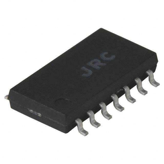
| 描述 | IC OPAMP CFA 600MHZ 16SOIC |
| 产品分类 | Linear - Amplifiers - Instrumentation, OP Amps, Buffer Amps |
| 品牌 | Intersil |
| 数据手册 | |
| 产品图片 |
|
| 产品型号 | EL5364ISZ-T7 |
| PCN组件/产地 | |
| rohs | 无铅 / 符合限制有害物质指令(RoHS)规范要求 |
| 产品系列 | - |
| 供应商器件封装 | 16-SOIC |
| 其它名称 | EL5364ISZ-T7DKR |
| 包装 | Digi-Reel® |
| 压摆率 | 4200 V/µs |
| 增益带宽积 | - |
| 安装类型 | 表面贴装 |
| 封装/外壳 | 16-SOIC(0.154",3.90mm 宽) |
| 工作温度 | -40°C ~ 85°C |
| 放大器类型 | 电流反馈 |
| 标准包装 | 1 |
| 电压-电源,单/双 (±) | 5 V ~ 12 V, ±2.5 V ~ 6 V |
| 电压-输入失调 | 1.5mV |
| 电流-电源 | 3.5mA |
| 电流-输入偏置 | 2µA |
| 电流-输出/通道 | 140mA |
| 电路数 | 3 |
| 输出类型 | - |


- 商务部:美国ITC正式对集成电路等产品启动337调查
- 曝三星4nm工艺存在良率问题 高通将骁龙8 Gen1或转产台积电
- 太阳诱电将投资9.5亿元在常州建新厂生产MLCC 预计2023年完工
- 英特尔发布欧洲新工厂建设计划 深化IDM 2.0 战略
- 台积电先进制程称霸业界 有大客户加持明年业绩稳了
- 达到5530亿美元!SIA预计今年全球半导体销售额将创下新高
- 英特尔拟将自动驾驶子公司Mobileye上市 估值或超500亿美元
- 三星加码芯片和SET,合并消费电子和移动部门,撤换高东真等 CEO
- 三星电子宣布重大人事变动 还合并消费电子和移动部门
- 海关总署:前11个月进口集成电路产品价值2.52万亿元 增长14.8%


PDF Datasheet 数据手册内容提取
DATASHEET EL5164, EL5165, EL5364 FN7389 600MHz Current Feedback Amplifiers with Enable Rev 9.00 January 30, 2014 The EL5164, EL5165, and EL5364 are current feedback Features amplifiers with a very high bandwidth of 600MHz. This makes these amplifiers ideal for today’s high speed video and monitor • 600MHz -3dB bandwidth applications. • 4700V/µs slew rate With a supply current of just 3.5mA per amplifier and the • 3.5mA supply current ability to run from a single supply voltage from 5V to 12V, • Single and dual supply operation, from 5V to 12V supply span these amplifiers are also ideal for handheld, portable or battery-powered equipment. • Fast enable/disable (EL5164 and EL5364 only) • Available in SOT-23 packages The EL5164 and EL5364 also incorporate an enable and disable function to reduce the supply current to 14µA typical • High speed, 1.4GHz product available (EL5166 and EL5167) per amplifier. Allowing the CE pin to float, or applying a low • 500MHz products available in Single (EL5162, EL5163), Dual logic level, enables the amplifier. (EL5262, EL5263) and Triple (EL5362) The EL5165 is offered in the 5 Ld SOT-23 package, EL5164 is • Pb-Free (RoHS compliant) available in the 6 Ld SOT-23 and the industry-standard 8 Ld SOIC Applications packages, and the EL5364 in a 16 Ld SOIC and 16 Ld QSOP packages. All operate over the industrial temperature range of • Video amplifiers -40°C to +85°C. • Cable drivers • RGB amplifiers • Test equipment • Instrumentation • Current to voltage converters Pin Configurations EL5164 EL5164 (8 LD SOIC) (6 LD SOT-23) TOP VIEW TOP VIEW NC 1 8 CE OUT 1 6 VS+ IN- 2 7 VS+ VS- 2 5 CE - + - + IN+ 3 6 OUT IN+ 3 4 IN- VS- 4 5 NC FN7389 Rev 9.00 Page 1 of 17 January 30, 2014
EL5164, EL5165, EL5364 Pin Configurations EL5165 EL5364 (5 LD SOT-23) (16 LD SOIC, QSOP) TOP VIEW TOP VIEW INA+ 1 16INA- OUT 1 5 VS+ - CEA 2 15OUTA VS- 2 + + - VS- 3 14VS+ IN+ 3 4 IN- + CEB 4 13OUTB - INB+ 5 12INB- NC 6 11 NC + CEC 7 10OUTC - INC+ 8 9 INC- Ordering Information PART NUMBER PART PACKAGE PKG. (Notes 2, 3) MARKING (Pb-free) DWG. # EL5164ISZ 5164ISZ 8 Ld SOIC (150 mil) M8.15E EL5164ISZ-T7 (Note 1) 5164ISZ 8 Ld SOIC (150 mil) M8.15E EL5164ISZ-T13 (Note 1) 5164ISZ 8 Ld SOIC (150 mil) M8.15E EL5164IWZ-T7 (Note 1) BAMA (Note 4) 6 Ld SOT-23 P6.064A EL5164IWZ-T7A (Note 1) BAMA (Note 4) 6 Ld SOT-23 P6.064A EL5165IWZ-T7 (Note 1) BANA (Note 4) 5 Ld SOT-23 P5.064A EL5165IWZ-T7A (Note 1) BANA (Note 4) 5 Ld SOT-23 P5.064A EL5364ISZ EL5364ISZ 16 Ld SOIC (150 mil) MDP0027 EL5364ISZ-T7 (Note 1) EL5364ISZ 16 Ld SOIC (150 mil) MDP0027 EL5364ISZ-T13 (Note 1) EL5364ISZ 16 Ld SOIC (150 mil) MDP0027 EL5364IUZ 5364IUZ 16 Ld QSOP (150 mil) MDP0040 EL5364IUZ-T7 (Note 1) 5364IUZ 16 Ld QSOP (150 mil) MDP0040 EL5364IUZ-T13 (Note 1) 5364IUZ 16 Ld QSOP (150 mil) MDP0040 EL5364IUZA 5364IUZ 16 Ld QSOP (150 mil) MDP0040 EL5364IUZA-T7 (Note 1) 5364IUZ 16 Ld QSOP (150 mil) MDP0040 EL5364IUZA-T13 (Note 1) 5364IUZ 16 Ld QSOP (150 mil) MDP0040 NOTES: 1. Please refer to TB347 for details on reel specifications. 2. These Intersil Pb-free plastic packaged products employ special Pb-free material sets, molding compounds/die attach materials, and 100% matte tin plate plus anneal (e3 termination finish, which is RoHS compliant and compatible with both SnPb and Pb-free soldering operations). Intersil Pb-free products are MSL classified at Pb-free peak reflow temperatures that meet or exceed the Pb-free requirements of IPC/JEDEC J STD-020. 3. For Moisture Sensitivity Level (MSL), please see product information page for EL5164, EL5165, EL5364. For more information on MSL, please see tech brief TB363. 4. The part marking is located on the bottom of the part. FN7389 Rev 9.00 Page 2 of 17 January 30, 2014
EL5164, EL5165, EL5364 Absolute Maximum Ratings Thermal Information (TA = +25°C) Supply Voltage between VS+ and VS-. . . . . . . . . . . . . . . . . . . . . . . . . . 13.2V Maximum Power Dissipation . . . . . . . . . . . . . . . . . . . see curves on page8 Maximum Continuous Output Current. . . . . . . . . . . . . . . . . . . . . . . . . 50mA Maximum Storage Temperature Range . . . . . . . . . . . . . -65°C to +150°C Pin Voltages. . . . . . . . . . . . . . . . . . . . . . . . . . . . . (VS-) - 0.5V to (VS+) + 0.5V Ambient Operating Temperature Range. . . . . . . . . . . . . . -40°C to +85°C Supply Slewrate between VS+ and VS-. . . . . . . . . . . . . . . . . . . . 1V/µs(Max) Maximum Operating Junction Temperature. . . . . . . . . . . . . . . . . . +125°C VIN-DIFF (VIN+ - VIN-) (When Disabled) . . . . . . . . . . . . . . . . . . . . . .±2V (Max) Pb-free reflow profile . . . . . . . . . . . . . . . . . . . . . . . . . . . . . . . . see link below http://www.intersil.com/pbfree/Pb-FreeReflow.asp CAUTION: Do not operate at or near the maximum ratings listed for extended periods of time. Exposure to such conditions may adversely impact product reliability and result in failures not covered by warranty Electrical Specifications VS+ = +5V, VS- = -5V, RF = 750 for AV = 1, RF = 375 for AV = 2, RL = 150, VCE = 0V, TA = +25°C unless otherwise specified. Boldface limits apply across the operating temperature range, -40°C to +85°C. MIN MAX PARAMETER DESCRIPTION CONDITIONS (Note 6) Typ (Note 6) UNIT AC PERFORMANCE BW -3dB Bandwidth AV = +1, RL = 500RF = 510 600 MHz AV = +2, RL = 150RF = 412 450 MHz BW1 0.1dB Bandwidth AV = +2, RL = 150RF = 412 50 MHz SR Slew Rate VOUT = -3V to +3V, AV = +2, RL=100 3500 4700 7000 V/µs (EL5164, EL5165) VOUT = -3V to +3V, AV = +2, RL=100 3000 4200 6000 V/µs (EL5364) tS 0.1% Settling Time VOUT = -2.5V to +2.5V, AV = +2, 15 ns RF = RG = 1k eN Input Voltage Noise f = 1MHz 2.1 nV/Hz iN- IN- Input Current Noise f = 1MHz 13 pA/Hz iN+ IN+ Input Current Noise f = 1MHz 13 pA/Hz HD2 5MHz, 2.5VP-P -81 dBc HD3 5MHz, 2.5VP-P -74 dBc dG Differential Gain Error (Note 5) AV = +2 0.01 % dP Differential Phase Error (Note 5) AV = +2 0.01 ° DC PERFORMANCE VOS Offset Voltage -5 1.5 +5 mV TCVOS Input Offset Voltage Temperature Measured from TMIN to TMAX 6 µV/°C Coefficient ROL Open Loop Transimpedance Gain 1.1 3 M INPUT CHARACTERISTICS CMIR Common Mode Input Range Guaranteed by CMRR test ±3 ±3.3 V CMRR Common Mode Rejection Ratio VIN = ±3V 50 62 75 dB -ICMR - Input Current Common Mode Rejection -1 0.1 +1 µA/V +IIN + Input Current -10 2 +10 µA -IIN - Input Current -10 2 +10 µA RIN Input Resistance + Input 300 650 1200 k CIN Input Capacitance 1 pF FN7389 Rev 9.00 Page 3 of 17 January 30, 2014
EL5164, EL5165, EL5364 Electrical Specifications VS+ = +5V, VS- = -5V, RF = 750 for AV = 1, RF = 375 for AV = 2, RL = 150, VCE = 0V, TA = +25°C unless otherwise specified. Boldface limits apply across the operating temperature range, -40°C to +85°C. (Continued) MIN MAX PARAMETER DESCRIPTION CONDITIONS (Note 6) Typ (Note 6) UNIT OUTPUT CHARACTERISTICS VO Output Voltage Swing RL = 150 to GND ±3.6 ±3.8 ±4.0 V RL = 1k to GND ±3.9 ±4.1 ±4.2 V IOUT Output Current RL = 10 to GND 100 140 190 mA SUPPLY ISON Supply Current - Enabled, per Amplifier No load, VIN = 0V 3.2 3.5 4.2 mA ISOFF+ Supply Current - Disabled, per Amplifier No load, VIN = 0V, EL5164 and EL5364 0 +25 µA Only ISOFF- Supply Current - Disabled, per Amplifier -25 -14 0 µA PSRR Power Supply Rejection Ratio DC, VS = ±4.75V to ±5.25V 65 79 dB -IPSR - Input Current Power Supply Rejection DC, VS = ±4.75V to ±5.25V -1 0.1 +1 µA/V ENABLE (EL5164, EL5364 ONLY) tEN Enable Time 200 ns tDIS Disable Time 800 ns IIHCE CE Pin Input High Current CE = VS+ 1 10 +25 µA IILCE CE Pin Input Low Current CE = (VS+) -5V -1 0 +1 µA VIHCE CE Input High Voltage for Power-down (VS+) - 1 V VILCE CE Input Low Voltage for Power-up (VS+) - 3 V NOTES: 5. Standard NTSC test, AC signal amplitude = 286mVP-P, f = 3.58MHz 6. Parameters with MIN and/or MAX limits are 100% tested at +25°C, unless otherwise specified. Temperature limits established by characterization and are not production tested. FN7389 Rev 9.00 Page 4 of 17 January 30, 2014
EL5164, EL5165, EL5364 Typical Performance Curves 5 5 4 ±VS = ±5V RF = 1.2k, C L= 5pF 4 ±VS = ±5V AV = +2 RF = 1.2k, CL = 3.5pF CL = 2.5pF AIN (dB) 123 RRFF == 11..22kk,, CCLL == 02..85ppFF AIN (dB) 123 AV = +5 RF = 160, RRGF = = 4 2120, RG = 55 G G D 0 D 0 ORMALIZE ---123 RRFF ==R F11 ..=58 kk2,,. 2CCkLL, ==C L00 ..=88 pp0FF.8pF ORMALIZE ---123 RRRFFF === 333069007,,, RRRGGG === 789577 N N RF = 412, RG = 100 -4 -4 RF = 560, RG = 135 -5 -5 100k 1M 10M 100M 1G 100k 1M 10M 100M 1G FREQUENCY (Hz) FREQUENCY (Hz) FIGURE 1. FREQUENCY RESPONSE FOR VARIOUS RF AND CL FIGURE 2. FREQUENCY RESPONSE FOR VARIOUS RF 6 5 5 ±VS = ±5V 4 VS+ = +5V B) 4 CAVL == +2.15pF B) 3 VCSL- = = 5 -p5FV RF = 412 AIN (d 23 RF = 510 AIN (d 21 ARVL == +1520 RF = 562 G G D 1 RF = 681 D 0 E E ALIZ 0 ALIZ -1 RF = 681 RM -1 RF = 750 RM -2 RF = 866 NO -2 RF = 909 NO -3 RF = 1.2k -3 RF = 1201 -4 RF = 1.5k -4 100k 1M 10M 100M 1G 100k 1M 10M 100M 1G FREQUENCY (Hz) FREQUENCY (Hz) FIGURE 3. FREQUENCY RESPONSE FOR VARIOUS RF FIGURE 4. FREQUENCY RESPONSE FOR VARIOUS RF 5 4 RL = 150 N (dB) 23 RRFG == 442222 E (V) INPUT 2V/DIV GAI 1 TUD D 0 LI E P Z M ALI -1 ±VS = 6V A RM -2 5V OUTPUT 1V/DIV NO -3 34VV ±AVVS = =+ ±25 V -4 2.5V RL = 150 -5 100k 1M 10M 100M 1G FREQUENCY (Hz) ns FIGURE 5. FREQUENCY RESPONSE FOR VARIOUS POWER FIGURE 6. OUTPUT RISE TIME SUPPLY VOLTAGES FN7389 Rev 9.00 Page 5 of 17 January 30, 2014
EL5164, EL5165, EL5364 Typical Performance Curves (Continued) 0 B) ---231000 VVAVSS +-= == + -+155VV dB) ---3210000 VVAVRVSSOL + -U== =T= +1 -=+015 50 2V VVP-P RR (d -40 TION ( -40 THD S R -50 P -50 O T S -60 -60 ±VS DI SECOND HARMONIC -70 -70 THIRD HARMONIC -80 -80 -90 1k 10k 100k 1M 10M 100M 0 10 20 30 40 50 60 FREQUENCY (Hz) FREQUENCY (MHz) FIGURE 7. PSRR vs FREQUENCY FIGURE 8. DISTORTION vs FREQUENCY (AV = +1) 0 dB) ---321000 VVAVRVSSOL +- U== =T= +1 -=+025 50V2VVP-P NCE () 110 VVAVSS +-= == + -+255VV N ( -40 DA O E RTI -50 THD MP 0.1 DISTO --7600 UTPUT I0.01 -80 O THIRD HARMONIC -90 SECOND HARMONIC -1000 10 20 30 40 50 60 10k 100k 1M 10M 100M FREQUENCY (MHz) FREQUENCY (Hz) FIGURE 9. DISTORTION vs FREQUENCY (AV = +2) FIGURE 10. OUTPUT IMPEDANCE vs FREQUENCY 10M ±VS = ±5V 1M z) H ±VS = ±6V V/ 10 n ) 100k ±5V E ( (OL ±4V OIS R 10k ±3V E N 1 ±2.5V G A T 1k OL V 0.1 100 10k 100k 1M 10M 100M 100 1k 10k 100k 1M FREQUENCY (Hz) FREQUENCY (Hz) FIGURE 11. OPEN LOOP TRANSIMPEDANCE GAIN (ROL) vs FIGURE 12. VOLTAGE NOISE vs FREQUENCY FREQUENCY FOR VARIOUS SUPPLY VOLTAGES FN7389 Rev 9.00 Page 6 of 17 January 30, 2014
EL5164, EL5165, EL5364 Typical Performance Curves (Continued) VS+ = +5V VS+ = +5V, VS- = -5V VS- = -5V AV = +2 z) RL = 150 H 100 A/ p E ( S CH1 OI N T 10 N E RR CH2 U C 1 100 1k 10k 100k FREQUENCY (Hz) FIGURE 13. CURRENT NOISE vs FREQUENCY FIGURE 14. TURN-ON DELAY, VIN = 100mVP-P 0.003 PHASE GAIN (%) 00..0000120 000...000000012 PHASE (°) CH1 ENTIAL --00..000012 GAIN --00..000021ENTIAL R R CH2 VVARVSSL +- == == +1 -+52550VV DIFFE -0.003 VATEVS +S= T= + F+2R5VE,Q VUSE- N= C-5YV, 3.58MHz ---000...000000345DIFFE 1V 0 -1V DC INPUT FIGURE 15. TURN-OFF DELAY, VIN = 100mVP-P FIGURE 16. DIFFERENTIAL GAIN/PHASE vs DC INPUT VOLTAGE AT 3.58MHz -30 4 VS+ = +5V -40 VS+ = +5V GAIN (dB) 123 VRRRCSLFGL- === == 145 4-p025202FV2 C K (dB) ---765000 VRRRSLFG - == == 14 4-025202V2 C TO B D L E 0 A -80 Z B T ALI -1 A OSS -90 A TO C RM -2 CR-100 A TO B O N -3 -110 -4 -120 -5 -130 10k 100k 1M 10M 100M 10k 100k 1M 10M 100M FREQUENCY (Hz) FREQUENCY (Hz) FIGURE 17. FREQUENCY RESPONSE FOR VARIOUS CHANNELS FIGURE 18. CROSSTALK BETWEEN CHANNELS (EL5364) (EL5364) FN7389 Rev 9.00 Page 7 of 17 January 30, 2014
EL5164, EL5165, EL5364 Typical Performance Curves (Continued) JEDEC JESD51-7 HIGH EFFECTIVE THERMAL JEDEC JESD51-7 HIGH EFFECTIVE THERMAL CONDUCTIVITY TEST BOARD CONDUCTIVITY TEST BOARD 1.4 1.4 1.250W SO16 (0.150”) W) 1.2 JA = +80°C/W W) 1.2 N ( 1.0 N ( 1.0 O O ATI 0.8 909mW ATI 0.8 893mW QSOP16 P P R DISSI 0.6 435mW JA = S+O1180°C/W R DISSI 0.6 JA = +112°C/W E 0.4 E 0.4 W W O O P 0.2 SOT23-5/6 P 0.2 JA = +230°C/W 0 0 0 25 50 7585 100 125 150 0 25 50 7585 100 125 150 AMBIENT TEMPERATURE (°C) AMBIENT TEMPERATURE (°C) FIGURE 19. PACKAGE POWER DISSIPATION vs AMBIENT FIGURE 20. PACKAGE POWER DISSIPATION vs AMBIENT TEMPERATURE TEMPERATURE JEDEC JESD51-3 LOW EFFECTIVE THERMAL JEDEC JESD51-3 LOW EFFECTIVE THERMAL CONDUCTIVITY TEST BOARD CONDUCTIVITY TEST BOARD 1.0 1.2 0.9 W) 0.8 W) 1.0 909mW POWER DISSIPATION ( 000000......642735 362951mmSWWOT23-5/6 JA = S+O1680°C/W POWER DISSIPATION ( 0000....8642 633mW JAJ QA= SS+=OO 1+51P16811 °0(6C0°C./1W/5W0”) 0.1 JA = +256°C/W 0 0 0 25 50 75 85 100 125 150 0 25 50 75 85 100 125 150 AMBIENT TEMPERATURE (°C) AMBIENT TEMPERATURE (°C) FIGURE 21. PACKAGE POWER DISSIPATION vs AMBIENT FIGURE 22. PACKAGE POWER DISSIPATION vs AMBIENT TEMPERATURE TEMPERATURE FN7389 Rev 9.00 Page 8 of 17 January 30, 2014
EL5164, EL5165, EL5364 Pin Descriptions EL5164 EL5164 EL5165 EL5364 (8 Ld SOIC) (6 Ld SOT-23) Pin Name Function Equivalent Circuit 1, 5 6, 11 NC Not connected 2 4 4 9, 12, 16 IN- Inverting input VS+ IN+ IN- VS- CIRCUIT 1 3 3 3 1, 5, 8 IN+ Non-inverting input (See circuit 1) 4 2 2 3 VS- Negative supply 6 1 1 10, 13, OUT Output VS+ 15 OUT VS- CIRCUIT 2 7 6 5 14 VS+ Positive supply 8 5 2, 4, 7 CE Chip enable, allowing the VS+ pin to float or applying a low logic level enables the corresponding amplifier. CE 0.5M INTERNAL 0V VS- CIRCUIT 3 Applications Information Power Supply Bypassing and Printed Circuit Board Layout Product Description As with any high frequency device, good printed circuit board The EL5164, EL5165, and EL5364 are current-feedback operational layout is necessary for optimum performance. Low impedance amplifiers that offer a wide -3dB bandwidth of 600MHz and a low ground plane construction is essential. Surface mount supply current of 3.5mA per amplifier. The EL5164, EL5165, and components are recommended, but if leaded components are EL5364 work with supply voltages ranging from a single 5V to 10V used, lead lengths should be as short as possible. The power and they are also capable of swinging to within 1V of either supply supply pins must be well bypassed to reduce the risk of on the output. Because of their current-feedback topology, the oscillation. The combination of a 4.7µF tantalum capacitor in EL5164, EL5165, and EL5364 do not have the normal gain- parallel with a 0.01µF capacitor has been shown to work well bandwidth product associated with voltage-feedback operational when placed at each supply pin. amplifiers. Instead, their -3dB bandwidth remains relatively For good AC performance, parasitic capacitance should be kept constant as closed-loop gain increases. This combination of high to a minimum, especially at the inverting input. (See the bandwidth and low power, together with aggressive pricing makes “Capacitance at the Inverting Input” on page10). Even when the EL5164, EL5165, and EL5364 ideal choices for many low- ground plane construction is used, it should be removed from the power/high-bandwidth applications such as portable, handheld, or area near the inverting input to minimize any stray capacitance battery-powered equipment. For varying bandwidth needs, consider at that node. Carbon or Metal-Film resistors are acceptable with the EL5166 and EL5167 with 1.4GHz bandwidth and an 8.5mA the Metal-Film resistors giving slightly less peaking and supply current, or the EL5162 and EL5163 with 500MHz bandwidth bandwidth because of additional series inductance. Use of and a 1.5mA supply current. Versions include single, dual, and triple sockets, particularly for the SO package, should be avoided if amp configurations with 5Ld SOT-23, 16 Ld QSOP, and 8 Ld SOIC possible. Sockets add parasitic inductance and capacitance or 16 Ld SOIC outlines. which results in additional peaking and overshoot. FN7389 Rev 9.00 Page 9 of 17 January 30, 2014
EL5164, EL5165, EL5364 Disable/Power-Down peaking can be easily modified by varying the value of the feedback resistor. The EL5164 and EL5364 amplifiers can be disabled, placing their outputs in a high impedance state. When disabled, the Because the EL5164, EL5165, and EL5364 are current-feedback amplifiers supply current reduces to <25µA per amplifier. An amplifiers, their gain-bandwidth product is not a constant for amplifier disables when its CE pin is pulled up to within 1V of the different closed-loop gains. This feature actually allows the positive supply. Similarly, the amplifier is enabled by floating or EL5164, EL5165, and EL5364 to maintain about the same -3dB pulling its CE pin to at least 3V below the positive supply. For a bandwidth. As gain is increased, bandwidth decreases slightly ±5V supply, this means that an amplifier enables when its CE is while stability increases. Since the loop stability is improving with 2V or less, and disables when CE is above 4V. Although the logic higher closed-loop gains, it becomes possible to reduce the value levels are not standard TTL, this choice of logic voltages allows of RF below the specified 412 and still retain stability, resulting the amplifiers to be enabled by tying CE to ground, even in 5V in only a slight loss of bandwidth with increased closed-loop gain. single supply applications. The CE pin can be driven from CMOS Supply Voltage Range and Single-Supply outputs. Operation When the amplifier is disabled, if the positive input is driven beyond ±2V with respect to the negative input, the device can The EL5164, EL5165, and EL5364 are designed to operate with become active and output the signal. An input diode clamp supply voltages having a span of 5V to 10V. In practical terms, network D1 and D2, as shown in Figure 23, can be used to keep this means that they will operate on dual supplies ranging from the device disabled while a large input signal is present. ±2.5V to ±5V. With a single-supply, the EL5164, EL5165, and EL5364 will operate from 5V to 10V. RG RF As supply voltages continue to decrease, it becomes necessary to +5V provide input and output voltage ranges that can get as close as possible to the supply voltages. The EL5164, EL5165, and EL5364 have an input range which extends to within 2V of either - D1 D2 CE VOUT supply. For example, on ±5V supplies, the EL5164, EL5165, and VIN + +5V EL5364 have an input range which spans ±3V. The output range of the EL5164, EL5165, and EL5364 is also quite large, extending to within 1V of the supply rail. On a ±5V supply, the -5V output is therefore capable of swinging from -4V to +4V. Single- FIGURE 23. DISABLED AMPLIFIER supply output range is larger because of the increased negative swing due to the external pull-down resistor to ground. Capacitance at the Inverting Input Any manufacturer’s high-speed voltage- or current-feedback Video Performance amplifier can be affected by stray capacitance at the inverting For good video performance, an amplifier must maintain the same input. For inverting gains, this parasitic capacitance has little output impedance and the same frequency response as DC levels effect because the inverting input is a virtual ground, but for non- are changed at the output. This is especially difficult when driving inverting gains, this capacitance (in conjunction with the a standard video load of 150, because of the change in output feedback and gain resistors) creates a pole in the feedback path current with DC level. Previously, good differential gain could only of the amplifier. This pole, if low enough in frequency, has the be achieved by running high idle currents through the output same destabilizing effect as a zero in the forward open-loop transistors (to reduce variations in output impedance.) These response. The use of large-value feedback and gain resistors currents were typically comparable to the entire 3.5mA supply exacerbates the problem by further lowering the pole frequency current of each EL5164, EL5165, and EL5364 amplifier. Special (increasing the possibility of oscillation.) circuitry has been incorporated in the EL5164, EL5165, and The EL5164, EL5165, and EL5364 are optimized for a 510 EL5364 to reduce the variation of output impedance with current feedback resistor at AV = +1. With the high bandwidth of these output. This results in dG and dP specifications of 0.01% and amplifiers, these resistor values might cause stability problems 0.01°, while driving 150 at a gain of 2. when combined with parasitic capacitance, thus ground plane is Video performance has also been measured with a 500 load at a not recommended around the inverting input pin of the amplifier. gain of +1. Under these conditions, the EL5164, EL5165, and EL5364 have dG and dP specifications of 0.01% and 0.01°, Feedback Resistor Values respectively. The EL5164, EL5165, and EL5364 have been designed and specified for a gain of +2 with RF approximately 412. This value of feedback resistor gives 450MHz of -3dB bandwidth at AV = 2 with 1dB of peaking. With AV = -2, an RF of 300 gives 275MHz of bandwidth with 1dB of peaking. Since the EL5164, EL5165, and EL5364 are current-feedback amplifiers, it is also possible to change the value of RF to get more bandwidth. As seen in the curves of “Frequency Response for Various RF”, bandwidth and FN7389 Rev 9.00 Page 10 of 17 January 30, 2014
EL5164, EL5165, EL5364 Output Drive Capability where: In spite of their low 3.5mA of supply current, the EL5164, EL5165, • VS = Supply voltage and EL5364 are capable of providing a minimum of ±100mA of • ISMAX = Maximum supply current of 4.2mA output current. With a minimum of ±100mA of output drive, the EL5164, EL5165, and EL5364 are capable of driving 50 loads to • VOUTMAX = Maximum output voltage (required) both rails, making it an excellent choice for driving isolation • RL = Load resistance transformers in telecommunications applications. Typical Application Circuits Driving Cables and Capacitive Loads When used as a cable driver, double termination is always 0.1µF recommended for reflection-free performance. For those +5V applications, the back-termination series resistor will decouple IN+ VS+ the EL5164, EL5165, and EL5364 from the cable and allow OUT IN- extensive capacitive drive. However, other applications may have VS- high capacitive loads without a back-termination resistor. In 0.1µF -5V these applications, a small resistor (usually between 5 and 50) can be placed in series with the output to eliminate most 375 5 peaking. The gain resistor (RG) can then be chosen to make up for any gain loss which may be created by this additional resistor at the output. In many cases it is also possible to simply increase +5V 0.1µF VOUT the value of the feedback resistor (RF) to reduce the peaking. Current Limiting IN+ VS+ OUT 5 IN- The EL5164, EL5165, and EL5364 have no internal output VS- 0.1µF current-limiting circuitry. If the output is shorted, it is possible to -5V exceed the Absolute Maximum Rating for output current or 375 375 power dissipation, potentially resulting in the destruction of the VIN device. FIGURE 24. INVERTING 200mA OUTPUT CURRENT DISTRIBUTION Power Dissipation AMPLIFIER With the high output drive capability of the EL5164, EL5165, and EL5364, it is possible to exceed the +125°C Absolute Maximum 375 375 junction temperature under certain very high load current 0.1µF conditions. Generally speaking when RL falls below about 25, it +5V is important to calculate the maximum junction temperature (TJMAX) for the application, to determine if power supply voltages, IN+ VS+ OUT load conditions, or package type need to be modified to remain IN- in the safe operating area. These parameters are calculated in VS- 0.1µF Equation 1: 375 -5V T = T + nPD (EQ. 1) JMAX MAX JA MAX 0.1µF 375 +5V where: VIN IN+ VS+ OUT • TMAX = Maximum ambient temperature IN- VOUT •JA = Thermal resistance of the package VS- 0.1µF -5V • n = Number of amplifiers in the package • PDMAX = Maximum power dissipation of each amplifier in the FIGURE 25. FAST-SETTLING PRECISION AMPLIFIER package PDMAX for each amplifier can be calculated in Equation 2: V OUTMAX PD = 2V I + V –V ---------------------------- MAX S SMAX S OUTMAX R L (EQ. 2) FN7389 Rev 9.00 Page 11 of 17 January 30, 2014
EL5164, EL5165, EL5364 0.1µF 0.1µF +5V +5V IN+ VS+ IN+ VS+ OUT OUT IN- IN- VS- VS- 0.1µF 0.1µF -5V -5V 375 162 0.1µF 375 375 VOUT+ 0.1µF 1k +5V 240 0.1µF +5V IINN+- VS+ OUT 162 VOUT- 0.1µF IN+ VS+ OUT VS- 1k IN- VOUT 0.1µF VS- -5V 0.1µF 375 375 -5V VIN 375 375 TRANSMITTER RECEIVER FIGURE 26. DIFFERENTIAL LINE DRIVER/RECEIVER © Copyright Intersil Americas LLC 2004-2014. All Rights Reserved. All trademarks and registered trademarks are the property of their respective owners. For additional products, see www.intersil.com/en/products.html Intersil products are manufactured, assembled and tested utilizing ISO9001 quality systems as noted in the quality certifications found at www.intersil.com/en/support/qualandreliability.html Intersil products are sold by description only. Intersil may modify the circuit design and/or specifications of products at any time without notice, provided that such modification does not, in Intersil's sole judgment, affect the form, fit or function of the product. Accordingly, the reader is cautioned to verify that datasheets are current before placing orders. Information furnished by Intersil is believed to be accurate and reliable. However, no responsibility is assumed by Intersil or its subsidiaries for its use; nor for any infringements of patents or other rights of third parties which may result from its use. No license is granted by implication or otherwise under any patent or patent rights of Intersil or its subsidiaries. For information regarding Intersil Corporation and its products, see www.intersil.com FN7389 Rev 9.00 Page 12 of 17 January 30, 2014
EL5164, EL5165, EL5364 Package Outline Drawing M8.15E 8 LEAD NARROW BODY SMALL OUTLINE PLASTIC PACKAGE Rev 0, 08/09 4 4.90 ± 0.10 A DETAIL "A" 0.22 ± 0.03 B 6.0 ± 0.20 3.90 ± 0.10 4 PIN NO.1 ID MARK 5 (0.35) x 45° 4° ± 4° 0.43 ± 0.076 1.27 0.25MC AB SIDE VIEW “B” TOP VIEW 1.75 MAX 1.45 ± 0.1 0.25 GAUGE PLANE C 0.175 ± 0.075 SEATING PLANE 0.10C SIDE VIEW “A 0.63 ±0.23 DETAIL "A" (1.27) (0.60) NOTES: (1.50) 1. Dimensions are in millimeters. Dimensions in ( ) for Reference Only. 2. Dimensioning and tolerancing conform to AMSE Y14.5m-1994. 3. Unless otherwise specified, tolerance : Decimal ± 0.05 (5.40) 4. Dimension does not include interlead flash or protrusions. Interlead flash or protrusions shall not exceed 0.25mm per side. 5. The pin #1 identifier may be either a mold or mark feature. 6. Reference to JEDEC MS-012. TYPICAL RECOMMENDED LAND PATTERN FN7389 Rev 9.00 Page 13 of 17 January 30, 2014
EL5164, EL5165, EL5364 Package Outline Drawing P6.064A 6 LEAD SMALL OUTLINE TRANSISTOR PLASTIC PACKAGE Rev 0, 2/10 1.90 0-3° 0.95 D 0.08-0.20 A 6 5 4 PIN 1 INDEX AREA 2.80 3 1.60 3 5 0.15 C D 2x (0.60) 1 2 3 0.20 C 2x SEE DETAIL X B 0.40 ±0.05 3 0.20 M C A-B D TOP VIEW END VIEW 10° TYP 5 0.15 C A-B (2 PLCS) 2.90 2x H 1.14 ±0.15 1.45 MAX C (0.25) GAUGE 0.10 C SEATING PLANE PLANE 0.05-0.15 SIDE VIEW DETAIL "X" 0.45±0.1 4 (0.60) (1.20) NOTES: (2.40) 1. Dimensions are in millimeters. Dimensions in ( ) for Reference Only. 2. Dimensioning and tolerancing conform to ASME Y14.5M-1994. 3. Dimension is exclusive of mold flash, protrusions or gate burrs. 4. Foot length is measured at reference to guage plane. 5. This dimension is measured at Datum “H”. 6. Package conforms to JEDEC MO-178AA. (0.95) (1.90) TYPICAL RECOMMENDED LAND PATTERN FN7389 Rev 9.00 Page 14 of 17 January 30, 2014
EL5164, EL5165, EL5364 Package Outline Drawing P5.064A 5 LEAD SMALL OUTLINE TRANSISTOR PLASTIC PACKAGE Rev 0, 2/10 1.90 0-3° D A 0.08-0.20 5 4 PIN 1 INDEX AREA 2.80 3 1.60 3 5 0.15 CD 2x 2 0.20 C (0.60) 2x 0.95 SEE DETAIL X B 0.40 ±0.05 3 END VIEW 0.20M C A-B D TOP VIEW 10° TYP (2 PLCS) 5 0.15 C A-B H 2.90 2x 1.45 MAX C 1.14 ±0.15 (0.25)GAUGE 0.10 C SEATING PLANE PLANE 0.45±0.1 4 SIDE VIEW 0.05-0.15 DETAIL "X" (0.60) (1.20) NOTES: 1. Dimensions are in millimeters. (2.40) Dimensions in ( ) for Reference Only. 2. Dimensioning and tolerancing conform to ASME Y14.5M-1994. 3. Dimension is exclusive of mold flash, protrusions or gate burrs. 4. Foot length is measured at reference to guage plane. 5. This dimension is measured at Datum “H”. 6. Package conforms to JEDEC MO-178AA. (0.95) (1.90) TYPICAL RECOMMENDED LAND PATTERN FN7389 Rev 9.00 Page 15 of 17 January 30, 2014
EL5164, EL5165, EL5364 Small Outline Package Family (SO) A D h X 45° NN (N/2)+1 A PIN #1 I.D. MARK E E1 c SEE DETAIL “X” 1 (N/2) B L1 0.010M C A B e H C A2 GAUGE SEATING PLANE 0.010 PLANE A1 L 4° ±4° 0.004 C 0.010M C A B b DETAIL X MDP0027 SMALL OUTLINE PACKAGE FAMILY (SO) INCHES SO16 SO16 (0.300”) SO20 SO24 SO28 SYMBOL SO-8 SO-14 (0.150”) (SOL-16) (SOL-20) (SOL-24) (SOL-28) TOLERANCE NOTES A 0.068 0.068 0.068 0.104 0.104 0.104 0.104 MAX - A1 0.006 0.006 0.006 0.007 0.007 0.007 0.007 0.003 - A2 0.057 0.057 0.057 0.092 0.092 0.092 0.092 0.002 - b 0.017 0.017 0.017 0.017 0.017 0.017 0.017 0.003 - c 0.009 0.009 0.009 0.011 0.011 0.011 0.011 0.001 - D 0.193 0.341 0.390 0.406 0.504 0.606 0.704 0.004 1, 3 E 0.236 0.236 0.236 0.406 0.406 0.406 0.406 0.008 - E1 0.154 0.154 0.154 0.295 0.295 0.295 0.295 0.004 2, 3 e 0.050 0.050 0.050 0.050 0.050 0.050 0.050 Basic - L 0.025 0.025 0.025 0.030 0.030 0.030 0.030 0.009 - L1 0.041 0.041 0.041 0.056 0.056 0.056 0.056 Basic - h 0.013 0.013 0.013 0.020 0.020 0.020 0.020 Reference - N 8 14 16 16 20 24 28 Reference - Rev. M 2/07 NOTES: 1. Plastic or metal protrusions of 0.006” maximum per side are not included. 2. Plastic interlead protrusions of 0.010” maximum per side are not included. 3. Dimensions “D” and “E1” are measured at Datum Plane “H”. 4. Dimensioning and tolerancing per ASME Y14.5M-1994 FN7389 Rev 9.00 Page 16 of 17 January 30, 2014
EL5164, EL5165, EL5364 Quarter Size Outline Plastic Packages Family (QSOP) MDP0040 A QUARTER SIZE OUTLINE PLASTIC PACKAGES FAMILY D N (N/2)+1 INCHES SYMBOL QSOP16 QSOP24 QSOP28 TOLERANCE NOTES L 0.025 0.025 0.025 ±0.009 - PIN #1 I.D. MARK L1 0.041 0.041 0.041 Basic - E E1 N 16 24 28 Reference - Rev. F 2/07 NOTES: 1 (N/2) 5. Plastic or metal protrusions of 0.006” maximum per side are not B included. 0.010 CAB 6. Plastic interlead protrusions of 0.010” maximum per side are not included. e 7. Dimensions “D” and “E1” are measured at Datum Plane “H”. H 8. Dimensioning and tolerancing per ASME Y14.5M-1994. C SEATING PLANE 0.004 C 0.007 CAB b L1 A c SEE DETAIL "X" 0.010 A2 GAUGE PLANE L A1 4°±4° DETAIL X MDP0040 QUARTER SIZE OUTLINE PLASTIC PACKAGES FAMILY INCHES SYMBOL QSOP16 QSOP24 QSOP28 TOLERANCE NOTES A 0.068 0.068 0.068 Max. - A1 0.006 0.006 0.006 ±0.002 - A2 0.056 0.056 0.056 ±0.004 - b 0.010 0.010 0.010 ±0.002 - c 0.008 0.008 0.008 ±0.001 - D 0.193 0.341 0.390 ±0.004 1, 3 E 0.236 0.236 0.236 ±0.008 - E1 0.154 0.154 0.154 ±0.004 2, 3 e 0.025 0.025 0.025 Basic - FN7389 Rev 9.00 Page 17 of 17 January 30, 2014