ICGOO在线商城 > 集成电路(IC) > 线性 - 放大器 - 仪表,运算放大器,缓冲器放大器 > AMC1100DUB
 Datasheet下载
- 型号: AMC1100DUB
- 制造商: Texas Instruments
- 库位|库存: xxxx|xxxx
- 要求:
| 数量阶梯 | 香港交货 | 国内含税 |
| +xxxx | $xxxx | ¥xxxx |
查看当月历史价格
查看今年历史价格
AMC1100DUB产品简介:
ICGOO电子元器件商城为您提供AMC1100DUB由Texas Instruments设计生产,在icgoo商城现货销售,并且可以通过原厂、代理商等渠道进行代购。 AMC1100DUB价格参考¥18.72-¥26.18。Texas InstrumentsAMC1100DUB封装/规格:线性 - 放大器 - 仪表,运算放大器,缓冲器放大器, 隔离 放大器 1 电路 差分 8-SOP。您可以下载AMC1100DUB参考资料、Datasheet数据手册功能说明书,资料中有AMC1100DUB 详细功能的应用电路图电压和使用方法及教程。
AMC1100DUB 是由 Texas Instruments(德州仪器)生产的一款隔离放大器,属于线性放大器类别中的仪表、运算放大器和缓冲器放大器。其主要应用场景包括以下方面:

 1. 医疗设备
   - 心电图(ECG)监测:AMC1100DUB 可用于高精度的生物电位信号采集,例如在心电图设备中隔离心脏电信号,确保患者与设备之间的电气安全。
   - 病人监护仪:在多参数监护仪中,该器件可以隔离和放大微弱的生理信号,同时防止干扰和噪声。

 2. 工业自动化
   - 电流传感器:AMC1100DUB 能够在电力监控系统中隔离并测量电流信号,适用于电机控制、变频器和电源管理系统。
   - 数据采集系统:用于工业环境中需要电气隔离的数据采集模块,保护敏感电路免受高压或噪声的影响。

 3. 能源管理
   - 智能电网:在电力计量和配电监控中,AMC1100DUB 提供高压隔离功能,确保准确测量电流和电压。
   - 太阳能逆变器:用于隔离光伏系统的直流侧和交流侧信号,实现高效能量转换的同时保障安全性。

 4. 汽车电子
   - 电池管理系统(BMS):在电动汽车中,AMC1100DUB 可以隔离和监测电池组的电压和电流,确保电池运行的安全性和稳定性。
   - 车载充电器:提供信号隔离功能,避免高压对低压控制电路的损害。

 5. 通信设备
   - 电源隔离:在通信基站或网络设备中,用于隔离电源和信号路径,减少电磁干扰并提高系统可靠性。
   - 信号调理:处理低电平信号并进行放大和隔离,以适应复杂的通信环境。

 核心优势
- 高共模抑制比(CMRR):能够有效抑制共模噪声,适合复杂电磁环境下的应用。
- 电气隔离:通过电容耦合技术实现高达 5kVrms 的隔离能力,确保人身和设备安全。
- 低功耗:适合对能效要求较高的便携式或电池供电设备。

综上所述,AMC1100DUB 广泛应用于需要高精度信号隔离和放大的领域,尤其适合涉及高压、噪声敏感或电气安全要求严格的场景。
| 参数 | 数值 |
| -3db带宽 | 100kHz |
| 产品目录 | 集成电路 (IC)半导体 |
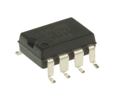
| 描述 | IC OPAMP ISOLATION 100KHZ 8SOP隔离放大器 4.25kV PEAK Iso Amp |
| 产品分类 | Linear - Amplifiers - Instrumentation, OP Amps, Buffer Amps集成电路 - IC |
| 品牌 | Texas Instruments |
| 产品手册 | http://www.ti.com/litv/sbas562 |
| 产品图片 |
|
| rohs | 符合RoHS无铅 / 符合限制有害物质指令(RoHS)规范要求 |
| 产品系列 | 放大器 IC,隔离放大器,Texas Instruments AMC1100DUB- |
| 数据手册 | |
| 产品型号 | AMC1100DUB |
| 产品种类 | 隔离放大器 |
| 供应商器件封装 | 8-SOP(2.54mm) |
| 共模抑制比—最小值 | 95 dB |
| 其它名称 | 296-30434-5 |
| 包装 | 管件 |
| 压摆率 | - |
| 商标 | Texas Instruments |
| 增益带宽积 | - |
| 安装类型 | 表面贴装 |
| 安装风格 | SMD/SMT |
| 封装 | Tube |
| 封装/外壳 | 8-SMD,鸥翼型 |
| 封装/箱体 | SOP-8 |
| 工作温度 | -40°C ~ 105°C |
| 工作温度范围 | - 40 C to + 105 C |
| 工作电源电压 | 3.3 V |
| 工厂包装数量 | 50 |
| 带宽 | 60 kHz |
| 放大器类型 | 隔离 |
| 标准包装 | 50 |
| 电压-电源,单/双 (±) | 2.7 V ~ 5.5 V |
| 电压-输入失调 | 200µV |
| 电流-电源 | 5.4mA |
| 电流-输入偏置 | - |
| 电流-输出/通道 | 20mA |
| 电源电流 | 8 mA |
| 电路数 | 1 |
| 系列 | AMC1100 |
| 输入补偿电压 | 1.5 mV |
| 输出类型 | 差分 |


PDF Datasheet 数据手册内容提取
Product Sample & Technical Tools & Support & Reference Folder Buy Documents Software Community Design AMC1100 SBAS562A–APRIL2012–REVISEDDECEMBER2014 AMC1100 Fully-Differential Isolation Amplifier 1 Features 3 Description • ±250-mVInputVoltageRangeOptimizedfor The AMC1100 is a precision isolation amplifier with 1 an output separated from the input circuitry by a ShuntResistors silicon dioxide (SiO ) barrier that is highly resistant to • VeryLowNonlinearity:0.075%maxat5V 2 magnetic interference. This barrier is certified to • LowOffsetError:1.5mVmax provide galvanic isolation of up to 4250 V , PEAK • LowNoise:3.1mV typ according to UL1577 and IEC60747-5-2. Used in RMS conjunction with isolated power supplies, this device • LowHigh-SideSupplyCurrent: prevents noise currents on a high common-mode 8mAmaxat5V voltage line from entering the local ground and • InputBandwidth:60kHzmin interferingwithordamagingsensitivecircuitry. • FixedGain:8(0.5%Accuracy) The AMC1100 input is optimized for direct connection • HighCommon-ModeRejectionRatio:108dB to shunt resistors or other low voltage level signal • Low-SideOperation:3.3V sources. The excellent performance of the device enables accurate current and voltage measurement • CertifiedGalvanicIsolation: in energy-metering applications. The output signal – UL1577andIEC60747-5-2Approved common-mode voltage is automatically adjusted to – IsolationVoltage:4250V eitherthe3-Vor5-Vlow-sidesupply. PEAK – WorkingVoltage:1200V The AMC1100 is fully specified over the extended PEAK – TransientImmunity:2.5kV/µsmin industrial temperature range of –40°C to +105°C and is available in the SMD-type, wide-body SOIC-8 • Typical10-YearLifeSpanatRatedWorking (DWV)andgullwing-8(DUB)packages. Voltage(seeApplicationReportSLLA197) • FullySpecifiedOvertheExtendedIndustrial DeviceInformation(1) TemperatureRange PARTNUMBER PACKAGE BODYSIZE(NOM) SOP(8) 9.50mm×6.57mm 2 Applications AMC1100 SOIC(8) 5.85mm×7.50mm • ShuntResistorBasedCurrentSensingin: (1) For all available packages, see the orderable addendum at – EnergyMeters theendofthedatasheet. – GreenEnergy – PowerMeasurementApplications Floating Power Supply HV+ AMC1100 Gate Driver 5.0 V VDD1 VDD2 3.3 V, or 5.0 V GND1 GND2 RSHUNT To Load VINP VOUTP ADS7263 VINN VOUTN Gate Driver HV- 1 An IMPORTANT NOTICE at the end of this data sheet addresses availability, warranty, changes, use in safety-critical applications, intellectualpropertymattersandotherimportantdisclaimers.PRODUCTIONDATA.
AMC1100 SBAS562A–APRIL2012–REVISEDDECEMBER2014 www.ti.com Table of Contents 1 Features.................................................................. 1 7.1 Overview.................................................................12 2 Applications........................................................... 1 7.2 FunctionalBlockDiagram.......................................12 3 Description............................................................. 1 7.3 FeatureDescription.................................................13 7.4 DeviceFunctionalModes........................................14 4 RevisionHistory..................................................... 2 8 ApplicationandImplementation........................ 15 5 PinConfigurationandFunctions......................... 3 8.1 ApplicationInformation............................................15 6 Specifications......................................................... 3 8.2 TypicalApplications................................................15 6.1 AbsoluteMaximumRatings......................................3 9 PowerSupplyRecommendations...................... 19 6.2 ESDRatings..............................................................3 10 Layout................................................................... 20 6.3 RecommendedOperatingConditions.......................4 6.4 ThermalInformation..................................................4 10.1 LayoutGuidelines.................................................20 6.5 RegulatoryInformation..............................................4 10.2 LayoutExample....................................................20 6.6 IEC60747-5-2InsulationCharacteristics.................4 11 DeviceandDocumentationSupport................. 21 6.7 IECSafetyLimitingValues.......................................5 11.1 DeviceSupport......................................................21 6.8 IEC61000-4-5Ratings.............................................5 11.2 DocumentationSupport........................................23 6.9 IEC60664-1Ratings.................................................5 11.3 Trademarks...........................................................23 6.10 PackageCharacteristics ........................................5 11.4 ElectrostaticDischargeCaution............................23 6.11 ElectricalCharacteristics.........................................6 11.5 Glossary................................................................23 6.12 TypicalCharacteristics............................................7 12 Mechanical,Packaging,andOrderable Information........................................................... 23 7 DetailedDescription............................................ 12 4 Revision History ChangesfromOriginal(April2012)toRevisionA Page • Changedformattomeetlatestdatasheetstandards............................................................................................................ 1 • AddedESDRatingtableandFeatureDescription,DeviceFunctionalModes,Applicationand Implementation,PowerSupplyRecommendations,Layout,DeviceandDocumentationSupport,andMechanical, Packaging,andOrderableInformationsections..................................................................................................................... 1 • AddedDWVpackagetodocument........................................................................................................................................ 1 • DeletedPackageandOrderingInformationsection............................................................................................................... 3 2 SubmitDocumentationFeedback Copyright©2012–2014,TexasInstrumentsIncorporated ProductFolderLinks:AMC1100
AMC1100 www.ti.com SBAS562A–APRIL2012–REVISEDDECEMBER2014 5 Pin Configuration and Functions DUBandDWVPackages SOP-8andSOIC-8 (TopView) VDD1 1 8 VDD2 VINP 2 7 VOUTP VINN 3 6 VOUTN GND1 4 5 GND2 PinDescriptions PIN FUNCTION NAME NO. DESCRIPTION GND1 4 Power High-sideanalogground GND2 5 Power Low-sideanalogground VDD1 1 Power High-sidepowersupply VDD2 8 Power Low-sidepowersupply VINN 3 Analoginput Invertinganaloginput VINP 2 Analoginput Noninvertinganaloginput VOUTN 6 Analogoutput Invertinganalogoutput VOUTP 7 Analogoutput Noninvertinganalogoutput 6 Specifications 6.1 Absolute Maximum Ratings overtheoperatingambienttemperaturerange(unlessotherwisenoted)(1) MIN MAX UNIT Supplyvoltage,VDD1toGND1orVDD2toGND2 –0.5 6 V AnaloginputvoltageatVINP,VINN GND1–0.5 VDD1+0.5 V Inputcurrenttoanypinexceptsupplypins ±10 mA Maximumjunctiontemperature,T Max 150 °C J Storagetemperaturerange,T –65 150 °C stg (1) StressesbeyondthoselistedunderAbsoluteMaximumRatingsmaycausepermanentdamagetothedevice.Thesearestressratings only,whichdonotimplyfunctionaloperationofthedeviceattheseoranyotherconditionsbeyondthoseindicatedunderRecommended OperatingConditions.Exposuretoabsolute-maximum-ratedconditionsforextendedperiodsmayaffectdevicereliability. 6.2 ESD Ratings VALUE UNIT Humanbodymodel(HBM),perANSI/ESDA/JEDECJS-001(1) ±2500 V(ESD) Electrostaticdischarge Chargeddevicemodel(CDM),perJEDECspecificationJESD22- V C101(2) ±1000 (1) JEDECdocumentJEP155statesthat500-VHBMallowssafemanufacturingwithastandardESDcontrolprocess. (2) JEDECdocumentJEP157statesthat250-VCDMallowssafemanufacturingwithastandardESDcontrolprocess. Copyright©2012–2014,TexasInstrumentsIncorporated SubmitDocumentationFeedback 3 ProductFolderLinks:AMC1100
AMC1100 SBAS562A–APRIL2012–REVISEDDECEMBER2014 www.ti.com 6.3 Recommended Operating Conditions overoperatingfree-airtemperaturerange(unlessotherwisenoted) MIN NOM MAX UNIT T Operatingambienttemperaturerange –40 105 °C A VDD1 High-sidepowersupply 4.5 5.0 5.5 V VDD2 Low-sidepowersupply 2.7 5.0 5.5 V 6.4 Thermal Information AMC1100 THERMALMETRIC(1) DUB(SOP) DWV(SOIC) UNIT 8PINS 8PINS R Junction-to-ambientthermalresistance 75.1 102.8 θJA R Junction-to-case(top)thermalresistance 61.6 49.8 θJC(top) R Junction-to-boardthermalresistance 39.8 56.6 θJB °C/W ψ Junction-to-topcharacterizationparameter 27.2 16.0 JT ψ Junction-to-boardcharacterizationparameter 39.4 55.2 JB R Junction-to-case(bottom)thermalresistance N/A N/A θJC(bot) (1) Formoreinformationabouttraditionalandnewthermalmetrics,seetheICPackageThermalMetricsapplicationreport,SPRA953. 6.5 Regulatory Information VDEANDIEC UL CSA Recognizedunder1577component RecognizedunderCSAcomponent CertifiedaccordingtoIEC60747-5-2 recognitionprogram acceptanceNO5program Filenumber:40016131 Filenumber:E181974 Filenumber:pending 6.6 IEC 60747-5-2 Insulation Characteristics overoperatingfree-airtemperaturerange(unlessotherwisenoted) PARAMETER TESTCONDITIONS VALUE UNIT V Maximumworkinginsulationvoltage 1200 V IORM PEAK Qualificationtest:afterinput/outputsafetytestsubgroup 1140 V 2/3V =V ×1.2,t=10s,partialdischarge<5pC PEAK PR IORM Qualificationtest:methodA,afterenvironmentaltests V Input-to-outputtestvoltage subgroup1,V =V ×1.6,t=10s,partialdischarge 1920 V PR PR IORM PEAK <5pC 100%productiontest:methodB1,V =V ×1.875, PR IORM 2250 V t=1s,partialdischarge<5pC PEAK V Transientovervoltage Qualificationtest:t=60s 4250 V IOTM PEAK Qualificationtest:V =V ,t=60s 4250 V TEST ISO PEAK V InsulationvoltageperUL ISO 100%productiontest:V =1.2xV ,t=1s 5100 V TEST ISO PEAK R Insulationresistance V =500V >109 Ω S IO PD Pollutiondegree 2 ° 4 SubmitDocumentationFeedback Copyright©2012–2014,TexasInstrumentsIncorporated ProductFolderLinks:AMC1100
AMC1100 www.ti.com SBAS562A–APRIL2012–REVISEDDECEMBER2014 6.7 IEC Safety Limiting Values Safetylimitingintendstopreventpotentialdamagetotheisolationbarrieruponfailureofinputoroutput(I/O)circuitry.I/O circuitryfailurecanallowlowresistancetoeithergroundorsupplyand,withoutcurrentlimiting,dissipatesufficientpowerto overheatthedieanddamagetheisolationbarrier,thuspotentiallyleadingtosecondarysystemfailures. Thesafety-limitingconstraintistheoperatingvirtualjunctiontemperaturerangespecifiedintheAbsoluteMaximumRatings table.Thepowerdissipationandjunction-to-airthermalimpedanceofthedeviceinstalledintheapplicationhardware determinethejunctiontemperature.Theassumedjunction-to-airthermalresistanceintheThermalInformationtableisthatof adeviceinstalledintheJESD51-3,LowEffectiveThermalConductivityTestBoardforLeadedSurface-MountPackagesand isconservative.Thepoweristherecommendedmaximuminputvoltagetimesthecurrent.Thejunctiontemperatureisthen theambienttemperatureplusthepowertimesthejunction-to-airthermalresistance. PARAMETER TESTCONDITIONS MIN TYP MAX UNIT I Safetyinput,output,orsupplycurrent θ =246°C/W,V =5.5V,T =+150°C,T =+25°C 10 mA S JA IN J A T Maximum-casetemperature +150 °C C 6.8 IEC 61000-4-5 Ratings PARAMETER TESTCONDITIONS VALUE UNIT V Surgeimmunity 1.2-μsor50-μsvoltagesurgeand8-μsor20-μscurrentsurge ±6000 V IOSM 6.9 IEC 60664-1 Ratings PARAMETER TESTCONDITIONS SPECIFICATION Basicisolationgroup Materialgroup II Ratedmainsvoltage≤150V I-IV RMS Ratedmainsvoltage≤300V I-IV RMS Installationclassification Ratedmainsvoltage≤400V I-III RMS Ratedmainsvoltage<600V I-III RMS 6.10 Package Characteristics(1) PARAMETER TESTCONDITIONS MIN TYP MAX UNIT Shortestterminal-to-terminaldistance L(I01) Minimumairgap(clearance) 7 mm throughair Shortestterminal-to-terminaldistance L(I02) Minimumexternaltracking(creepage) 7 mm acrosspackagesurface Trackingresistance CTI DINIEC60112andVDE0303part1 >400 V (comparativetrackingindex) Minimuminternalgap Distancethroughinsulation 0.014 mm (internalclearance) Inputtooutput,V =500V,allpinson IO eachsideofthebarriertiedtogetherto >1012 Ω RIO Isolationresistance createatwo-terminaldevice,TA<+85°C Inputtooutput,VIO=500V, >1011 Ω +85°C≤T <T max A A C Barriercapacitanceinputtooutput V =0.5V at1MHz 1.2 pF IO I PP C Inputcapacitancetoground V =0.5V at1MHz 3 pF I I PP (1) Creepageandclearancerequirementsshouldbeappliedaccordingtothespecificequipmentisolationstandardsofaspecific application.Careshouldbetakentomaintainthecreepageandclearancedistanceoftheboarddesigntoensurethatthemounting padsoftheisolatorontheprintedcircuitboard(PCB)donotreducethisdistance.CreepageandclearanceonaPCBbecomeequal accordingtothemeasurementtechniquesshownintheIsolationGlossarysection.Techniquessuchasinsertinggroovesorribsonthe PCBareusedtohelpincreasethesespecifications. Copyright©2012–2014,TexasInstrumentsIncorporated SubmitDocumentationFeedback 5 ProductFolderLinks:AMC1100
AMC1100 SBAS562A–APRIL2012–REVISEDDECEMBER2014 www.ti.com 6.11 Electrical Characteristics AllminimumandmaximumspecificationsareatT =–40°Cto+105°Candarewithinthespecifiedvoltagerange,unless A otherwisenoted.TypicalvaluesareatT =+25°C,VDD1=5V,andVDD2=3.3V. A PARAMETER TESTCONDITIONS MIN TYP MAX UNIT INPUT Maximuminputvoltagebefore VINP–VINN ±320 mV clipping Differentialinputvoltage VINP–VINN –250 250 mV V Common-modeoperatingrange –0.16 VDD1 V CM V Inputoffsetvoltage –1.5 ±0.2 1.5 mV OS TCV Inputoffsetthermaldrift –10 ±1.5 10 µV/K OS V from0Vto5Vat0Hz 108 dB IN CMRR Common-moderejectionratio V from0Vto5Vat50kHz 95 dB IN C InputcapacitancetoGND1 VINPorVINN 3 pF IN C Differentialinputcapacitance 3.6 pF IND R Differentialinputresistance 28 kΩ IN Small-signalbandwidth 60 100 kHz OUTPUT Nominalgain 8 Initial,atT =+25°C –0.5% ±0.05% 0.5% A G Gainerror ERR –1% ±0.05% 1% TCG Gainerrorthermaldrift ±56 ppm/K ERR 4.5V≤VDD2≤5.5V –0.075% ±0.015% 0.075% Nonlinearity 2.7V≤VDD2≤3.6V –0.1% ±0.023% 0.1% Nonlinearitythermaldrift 2.4 ppm/K Outputnoise VINP=VINN=0V 3.1 mV RMS vsVDD1,10-kHzripple 80 dB PSRR Power-supplyrejectionratio vsVDD2,10-kHzripple 61 dB Rise-and-falltime 0.5-Vstep,10%to90% 3.66 6.6 µs 0.5-Vstep,50%to10%,unfilteredoutput 1.6 3.3 µs V toV signaldelay 0.5-Vstep,50%to50%,unfilteredoutput 3.15 5.6 µs IN OUT 0.5-Vstep,50%to90%,unfilteredoutput 5.26 9.9 µs Common-modetransient CMTI V =1kV 2.5 3.75 kV/µs immunity CM 2.7V≤VDD2≤3.6V 1.15 1.29 1.45 V Outputcommon-modevoltage 4.5V≤VDD2≤5.5V 2.4 2.55 2.7 V Short-circuitcurrent 20 mA R Outputresistance 2.5 Ω OUT POWERSUPPLY VDD1 High-sidesupplyvoltage 4.5 5.0 5.5 V VDD2 Low-sidesupplyvoltage 2.7 5.0 5.5 V I High-sidesupplycurrent 5.4 8 mA DD1 2.7V<VDD2<3.6V 3.8 6 mA I Low-sidesupplycurrent DD2 4.5V<VDD2<5.5V 4.4 7 mA P High-sidepowerdissipation 27.0 44.0 mW DD1 2.7V<VDD2<3.6V 11.4 21.6 mW P Low-sidepowerdissipation DD2 4.5V<VDD2<5.5V 22.0 38.5 mW 6 SubmitDocumentationFeedback Copyright©2012–2014,TexasInstrumentsIncorporated ProductFolderLinks:AMC1100
AMC1100 www.ti.com SBAS562A–APRIL2012–REVISEDDECEMBER2014 6.12 Typical Characteristics AtVDD1=VDD2=5V,VINP=–250mVto+250mV,andVINN=0V,unlessotherwisenoted. 2 2 VDD2 = 2.7 V to 3.6 V 1.5 1.5 1 1 V) V) m 0.5 m 0.5 et ( et ( Offs 0 Offs 0 ut −0.5 ut −0.5 p p n n I I −1 −1 −1.5 −1.5 −2 −2 4.5 4.75 5 5.25 5.5 2.7 3 3.3 3.6 VDD1 (V) VDD2 (V) Figure1.InputOffsetvsHigh-SideSupplyVoltage Figure2.InputOffsetvsLow-SideSupplyVoltage 2 2 VDD2 = 4.5 V to 5.5 V 1.5 1.5 1 1 V) V) m 0.5 m 0.5 et ( et ( Offs 0 Offs 0 ut −0.5 ut −0.5 p p n n I I −1 −1 −1.5 −1.5 −2 −2 4.5 4.75 5 5.25 5.5 −40 −25 −10 5 20 35 50 65 80 95 110 125 VDD2 (V) Temperature (°C) Figure3.InputOffsetvsLow-SideSupplyVoltage Figure4.InputOffsetvsTemperature 130 40 120 30 110 20 A) dB) 100 nt (µ 10 RR ( 90 urre 0 M C C 80 ut −10 p n I 70 −20 60 −30 50 −40 0.1 1 10 100 −400 −300 −200 −100 0 100 200 300 400 Input Frequency (kHz) Input Voltage (mV) Figure5.Common-ModeRejectionRatiovs Figure6.InputCurrentvsInputVoltage InputFrequency Copyright©2012–2014,TexasInstrumentsIncorporated SubmitDocumentationFeedback 7 ProductFolderLinks:AMC1100
AMC1100 SBAS562A–APRIL2012–REVISEDDECEMBER2014 www.ti.com Typical Characteristics (continued) AtVDD1=VDD2=5V,VINP=–250mVto+250mV,andVINN=0V,unlessotherwisenoted. 120 1 0.8 110 0.6 Hz) 0.4 dwidth (k 19000 Error (%) 0.02 Ban ain −0.2 ut 80 G p −0.4 n I −0.6 70 −0.8 60 −1 −40 −25 −10 5 20 35 50 65 80 95 110 125 4.5 4.75 5 5.25 5.5 Temperature (°C) VDD1 (V) Figure7.InputBandwidthvsTemperature Figure8.GainErrorvsHigh-SideSupplyVoltage 1 1 VDD2 = 2.7 V to 3.6 V VDD2 = 4.5 V to 5.5 V 0.8 0.8 0.6 0.6 0.4 0.4 %) %) or ( 0.2 or ( 0.2 Err 0 Err 0 ain −0.2 ain −0.2 G G −0.4 −0.4 −0.6 −0.6 −0.8 −0.8 −1 −1 2.7 3 3.3 3.6 4.5 4.75 5 5.25 5.5 VDD2 (V) VDD2 (V) Figure9.GainErrorvsLow-SideSupplyVoltage Figure10.GainErrorvsLow-SideSupplyVoltage 1 10 0.8 0 0.6 −10 0.4 B) or (%) 0.2 Gain (d −−3200 ain Err −0.20 alized −40 G −0.4 orm −50 N −0.6 −60 −0.8 −70 −1 −80 −40 −25 −10 5 20 35 50 65 80 95 110 125 1 10 100 500 Temperature (°C) Input Frequency (kHz) Figure11.GainErrorvsTemperature Figure12.NormalizedGainvsInputFrequency 8 SubmitDocumentationFeedback Copyright©2012–2014,TexasInstrumentsIncorporated ProductFolderLinks:AMC1100
AMC1100 www.ti.com SBAS562A–APRIL2012–REVISEDDECEMBER2014 Typical Characteristics (continued) AtVDD1=VDD2=5V,VINP=–250mVto+250mV,andVINN=0V,unlessotherwisenoted. 0 5 −30 4.5 VOUTP VOUTN −60 4 −90 Output Phase (°) −−−−−221114185200000 Output Voltage (V) 123...52535 −270 1 −300 −330 0.5 −360 0 1 10 100 1000 −400 −300 −200 −100 0 100 200 300 400 Input Frequency (kHz) Input Voltage (mV) Figure13.OutputPhasevsInputFrequency Figure14.OutputVoltagevsInputVoltage 3.6 0.1 3.3 VDD2 = 2.7 V to 3.6 V VOUTP 0.08 VOUTN 3 0.06 2.7 oltage (V) 122...814 arity (%) 00..00024 V e utput 11..25 Nonlin −0.02 O −0.04 0.9 −0.06 0.6 0.3 −0.08 0 −0.1 −400 −300 −200 −100 0 100 200 300 400 4.5 4.75 5 5.25 5.5 Input Voltage (mV) VDD1 (V) Figure15.OutputVoltagevsInputVoltage Figure16.NonlinearityvsHigh-SideSupplyVoltage 0.1 0.1 VDD2 = 2.7 V to 3.6 V VDD2 = 4.5 V to 5.5 V 0.08 0.08 0.06 0.06 0.04 0.04 %) %) y ( 0.02 y ( 0.02 arit 0 arit 0 e e n n nli −0.02 nli −0.02 o o N N −0.04 −0.04 −0.06 −0.06 −0.08 −0.08 −0.1 −0.1 2.7 3 3.3 3.6 4.5 4.75 5 5.25 5.5 VDD2 (V) VDD2 (V) Figure17.NonlinearityvsLow-SideSupplyVoltage Figure18.NonlinearityvsLow-SideSupplyVoltage Copyright©2012–2014,TexasInstrumentsIncorporated SubmitDocumentationFeedback 9 ProductFolderLinks:AMC1100
AMC1100 SBAS562A–APRIL2012–REVISEDDECEMBER2014 www.ti.com Typical Characteristics (continued) AtVDD1=VDD2=5V,VINP=–250mVto+250mV,andVINN=0V,unlessotherwisenoted. 0.1 0.1 VDD2 = 3 V 0.08 0.08 VDD2 = 5 V 0.06 0.06 0.04 0.04 %) %) y ( 0.02 y ( 0.02 arit 0 arit 0 e e n n nli −0.02 nli −0.02 o o N N −0.04 −0.04 −0.06 −0.06 −0.08 −0.08 −0.1 −0.1 −250 −200 −150 −100 −50 0 50 100 150 200 250 −40 −25 −10 5 20 35 50 65 80 95 110 125 Input Voltage (mV) Temperature (°C) Figure19.NonlinearityvsInputVoltage Figure20.NonlinearityvsTemperature 2600 100 VDD1 2400 90 VDD2 2200 80 z)) 2000 70 H qrt( 1800 dB) 60 V/s 1600 R ( 50 n R e ( 1400 PS 40 s Noi 1200 30 1000 20 800 10 600 0 0.1 1 10 100 1 10 100 Frequency (kHz) Ripple Frequency (kHz) Figure21.OutputNoiseDensityvsFrequency Figure22.Power-SupplyRejectionRatiovs RippleFrequency 10 9 s) 8 µ e ( 7 500 mV/div m Ti 6 Fall 5 e/ Ris 4 put 3 ut 200 mV/div O 2 1 0 500 mV/div −40 −25 −10 5 20 35 50 65 80 95 110 125 Temperature (°C) Time (2ms/div) Figure23.OutputRiseandFallTimevsTemperature Figure24.Full-ScaleStepResponse 10 SubmitDocumentationFeedback Copyright©2012–2014,TexasInstrumentsIncorporated ProductFolderLinks:AMC1100
AMC1100 www.ti.com SBAS562A–APRIL2012–REVISEDDECEMBER2014 Typical Characteristics (continued) AtVDD1=VDD2=5V,VINP=–250mVto+250mV,andVINN=0V,unlessotherwisenoted. 10 5 50% to 10% VDD2 rising 9 50% to 50% V) VDD2 falling 8 50% to 90% e ( 4 g a s) 7 Volt Delay (µ 56 −Mode 3 nal 4 mon 2 g m Si 3 Co 2 put 1 ut 1 O 0 0 −40 −25 −10 5 20 35 50 65 80 95 110 125 3.5 3.6 3.7 3.8 3.9 4 4.1 4.2 4.3 4.4 4.5 Temperature (°C) VDD2 (V) Figure25.OutputSignalDelayTimevsTemperature Figure26.OutputCommon-ModeVoltagevs Low-SideSupplyVoltage 5 8 VDD2 = 2.7 V to 3.6 V IDD1 V) VDD2 = 4.5 V to 5.5 V 7 IDD2 e ( 4 ag 6 olt A) V m −Mode 3 urrent ( 45 n C mmo 2 pply 3 o u C S put 1 2 Out 1 0 0 −40 −25 −10 5 20 35 50 65 80 95 110 125 4.5 4.75 5 5.25 5.5 Temperature (°C) Supply Voltage (V) Figure27.OutputCommon-ModeVoltagevsTemperature Figure28.SupplyCurrentvsSupplyVoltage 8 8 VDD2 = 2.7 V to 3.6 V 7 7 6 6 A) m A) 5 nt ( 5 m e D2 ( 4 Curr 4 D y I 3 pl 3 p u S 2 2 1 1 IDD1 IDD2 0 0 2.7 3 3.3 3.6 −40 −25 −10 5 20 35 50 65 80 95 110 125 VDD2 (V) Temperature (°C) Figure29.Low-SideSupplyCurrentvs Figure30.SupplyCurrentvsTemperature Low-SideSupplyVoltage Copyright©2012–2014,TexasInstrumentsIncorporated SubmitDocumentationFeedback 11 ProductFolderLinks:AMC1100
AMC1100 SBAS562A–APRIL2012–REVISEDDECEMBER2014 www.ti.com 7 Detailed Description 7.1 Overview The AMC1100 consists of a delta-sigma modulator input stage including an internal reference and clock generator. The output of the modulator and clock signal are differentially transmitted over the integrated capacitive isolation barrier that separates the high- and low-voltage domains. The received bitstream and clock signals are synchronized and processed by a third-order analog filter with a nominal gain of 8 on the low-side andpresentedasadifferentialoutputofthedevice,asshownintheFunctionalBlockDiagram section. The SiO -based capacitive isolation barrier supports a high level of magnetic field immunity, as described in 2 application report SLLA181, ISO72x Digital Isolator Magnetic-Field Immunity (available for download at www.ti.com). 7.2 Functional Block Diagram VDD1 VDD2 Isolation Barrier 2.56-V 2.5-V Reference Reference DATA TX RX VINP Retiming and VOUTP û(cid:8)-Modulator 3rd order active VINN low-pass filter VOUTN TX RX CLK RC oscillator GND1 GND2 12 SubmitDocumentationFeedback Copyright©2012–2014,TexasInstrumentsIncorporated ProductFolderLinks:AMC1100
AMC1100 www.ti.com SBAS562A–APRIL2012–REVISEDDECEMBER2014 7.3 Feature Description The differential analog input of the AMC1100 is a switched-capacitor circuit based on a second-order modulator stage that digitizes the input signal into a 1-bit output stream. The device compares the differential input signal (V = VINP – VINN) against the internal reference of 2.5 V using internal capacitors that are continuously IN charged and discharged with a typical frequency of 10 MHz. With the S1 switches closed, C charges to the IND voltage difference across VINP and VINN. For the discharge phase, both S1 switches open first and then both S2 switches close. C discharges to approximately GND1 + 0.8 V during this phase. Figure 31 shows the IND simplifiedequivalentinputcircuitry. VDD1 GND1 GND1 CINP = 3 pF Equivalent 3 pF 400 : Curcuit GND1 + 0.8 V S1 S2 CIND = 3.6 pF RIN = 28 k: 400 : GND1 + 0.8 V S1 S2 3 pF CINN = 3 pF R 1 IN fCLK*CIND GND1 GND1 GND1 (fCLK = 10 MHz) Figure31. EquivalentInputCircuit The analog input range is tailored to directly accommodate a voltage drop across a shunt resistor used for current sensing. However, there are two restrictions on the analog input signals, VINP and VINN. If the input voltage exceeds the range GND1 – 0.5 V to VDD1 + 0.5 V, the input current must be limited to 10 mA to protect the implemented input protection diodes from damage. In addition, the device linearity and noise performance areensuredonlywhenthedifferentialanaloginputvoltageremainswithin ±250mV. Copyright©2012–2014,TexasInstrumentsIncorporated SubmitDocumentationFeedback 13 ProductFolderLinks:AMC1100
AMC1100 SBAS562A–APRIL2012–REVISEDDECEMBER2014 www.ti.com 7.4 Device Functional Modes The AMC1100 is powered on when the supplies are connected. The device is operated off a 5-V nominal supply on the high-side. The potential of the ground reference GND1 can be floating, which is usually the case in shunt- based current-measurement applications. TI recommends tying one side of the shunt to the GND1 pin of the AMC1100tomaintaintheoperatingcommon-moderangerequirementsofthedevice. The low-side of the AMC1100 can be powered from a supply source with a nominal voltage of 3.0 V, 3.3 V, or 5.0 V. When operated at 5 V, the common-mode voltage of the output stage is set to 2.55 V nominal; in both othercases,thecommon-modevoltageisautomaticallysetto1.29V. Although usually applied in shunt-based current-sensing circuits, the AMC1100 can also be used for isolated voltage measurement applications, as shown in a simplified way in Figure 32. In such applications, usually a resistor divider (R and R in Figure 32) is used to match the relatively small input voltage range of the 1 2 AMC1100. R and the AMC1100 input resistance (R ) also create a resistance divider that results in additional 2 IN gain error. With the assumption that R and R have a considerably higher value than R , the resulting total gain 1 IN 2 errorcanbeestimatedusingEquation1: R G = G + 2 ERRTOT ERR R IN where: • G =devicegainerror. (1) ERR L1 R 1 R R 2 IN L2 Figure32. VoltageMeasurementApplication 14 SubmitDocumentationFeedback Copyright©2012–2014,TexasInstrumentsIncorporated ProductFolderLinks:AMC1100
AMC1100 www.ti.com SBAS562A–APRIL2012–REVISEDDECEMBER2014 8 Application and Implementation NOTE Information in the following applications sections is not part of the TI component specification, and TI does not warrant its accuracy or completeness. TI’s customers are responsible for determining suitability of components for their purposes. Customers should validateandtesttheirdesignimplementationtoconfirmsystemfunctionality. 8.1 Application Information The AMC1100 offers unique linearity, high input common-mode rejection, and low dc errors and drift. These featuresmaketheAMC1100arobust,high-performanceisolationamplifierforindustrialapplicationswhereusers andsubsystemsmustbeprotectedfromhighvoltagepotentials. 8.2 Typical Applications 8.2.1 TheAMC1100inFrequencyInverters A typical operation for the AMC1100 is isolated current and voltage measurement in frequency inverter applications (such as industrial motor drives, photovoltaic inverters, or uninterruptible power supplies), as conceptually shown in Figure 33. Depending on the end application, only two or three phase currents are being sensed. DC Link Gate Driver Gate Driver Gate Driver RSHUNT RSHUNT RSHUNT AMC1100 Gate Driver Gate Driver Gate Driver VDD1 VDD2 GND1 GND2 VINP VOUTP ADC1P AMC1100 VINN VOUTN ADC1N VDD1 VDD2 AMC1100 GND1 GND2 VDD1 VDD2 VINP VOUTP ADC2P AMC1100 GND1 GND2 VINN VOUTN ADC2N VDD1 VDD2 VINP VOUTP ADC3P GND1 GND2 VINN VOUTN ADC3N VINP VOUTP ADC4P VINN VOUTN ADC4N Figure33. IsolatedCurrentandVoltageSensinginFrequencyInverters 8.2.1.1 DesignRequirements Current measurement through the phase of a motor power line is done via the shunt resistor R (in a two- SHUNT terminal shunt); see Figure 34. For better performance, the differential signal is filtered using RC filters (components R , R , and C ). Optionally, C and C can be used to reduce charge dumping from the inputs. In 2 3 2 3 4 this case, care must be taken when choosing the quality of these capacitors; mismatch in values of these capacitors leads to a common-mode error at the modulator input. Using NP0 capacitors is recommended, if necessary. Copyright©2012–2014,TexasInstrumentsIncorporated SubmitDocumentationFeedback 15 ProductFolderLinks:AMC1100
AMC1100 SBAS562A–APRIL2012–REVISEDDECEMBER2014 www.ti.com Typical Applications (continued) Phase Isolation Barrier TMC320 R C/F28xxx 1 Device 1 14 VDD1 VDD2 R C(1) C(1) 2 1 5 12W 0.1mF 0.1mF R 2 13 VINP VOUTP RSHUNT 1R23W 3C320(1 )pF R C ADC 3 11 VINN VOUTN C C 3 4 10 pF 10 pF (optional) (optional) 4 9 GND1 GND2 Figure34. Shunt-BasedCurrentSensingwiththeAMC1100 TheisolatedvoltagemeasurementcanbeperformedasdescribedintheDeviceFunctionalModes section. 8.2.1.2 DetailedDesignProcedure The floating ground reference (GND1) is derived from the end of the shunt resistor, which is connected to the negative input of the AMC1100 (VINN). If a four-terminal shunt is used, the inputs of the AMC1100 are connected to the inner leads and GND1 is connected to one of the outer shunt leads. The differential input of the AMC1100ensuresaccurateoperationeveninnoisyenvironments. The differential output of the AMC1100 can either directly drive an analog-to-digital converter (ADC) input or can befurtherfilteredbeforebeingprocessedbytheADC. 8.2.1.3 ApplicationCurve In frequency inverter applications the power switches must be protected in case of an overcurrent condition. To allowfastpoweringoffofthesystem,lowdelaycausedbytheisolationamplifierisrequired.Figure35 showsthe typicalfull-scalestepresponseoftheAMC1100. 500 mV/div 200 mV/div 500 mV/div Time (2ms/div) Figure35.TypicalStepResponseoftheAMC1100 16 SubmitDocumentationFeedback Copyright©2012–2014,TexasInstrumentsIncorporated ProductFolderLinks:AMC1100
AMC1100 www.ti.com SBAS562A–APRIL2012–REVISEDDECEMBER2014 Typical Applications (continued) 8.2.2 TheAMC1100inEnergyMetering Resulting from its immunity to magnetic fields, the AMC1100 can be used for shunt-based current sensing in smart electricity meter (e-meter) designs, as shown in Figure 36. Three AMC1100 devices are used for isolated current sensing. For voltage sensing, resistive dividers are usually used to reduce the common-mode voltage to levelsthatallownon-isolatedmeasurement. L1 L2 L3 VDD2 = DVDD VDD1A AMC1100 4G-Modulator VDD1B AMC1100 3x dig. filter for ADC currents MSP430F47167 DVDD Metrology MCU VDD1C AMC1100 ADC Sync ADC SysCLK 3x dig. filter for Application ADC voltage Data MCU ADC ADC Digital Core N Figure36. TheAMC1100inanE-MeterApplication 8.2.2.1 DesignRequirements For best performance, an RC low-pass filter can be used in front of the AMC1100. Further improvement can be achieved by filtering the output signal of the device. In both cases, the values of the resistors and the capacitors mustbetailoredtothebandwidthrequirementsofthesystem. Copyright©2012–2014,TexasInstrumentsIncorporated SubmitDocumentationFeedback 17 ProductFolderLinks:AMC1100
AMC1100 SBAS562A–APRIL2012–REVISEDDECEMBER2014 www.ti.com Typical Applications (continued) The analog output of the device is converted to the digital domain using the on-chip analog-to-digital converters (ADCs) of a suitable metrology microcontroller. The architecture of the MSP430F471x7 family of ultra-low power microcontrollers is tailored for this kind of applications. The MSP430F471x7 offers up to seven ADCs for simultaneous sampling: six of which are used for the three phase currents and voltages whereas the seventh channel can be used for additional voltage sensing of the neutral line for applications that require anti-tampering measures. 8.2.2.2 DetailedDesignProcedure The high-side supply for the AMC1100 can be derived from the phase voltage using a capacitive-drop power supply (cap-drop), as shown in Figure 37 and described in the application report SLAA552, AMC1100: ReplacementofInputMainSensingTransformerinInverterswithIsolateAmplifier. Phase 5.1 V 470 n / 400 V 220 1N4007 5.6V 470 µ / 10 V Neutral GND Figure37. Cap-DropHigh-SidePowerSupplyfortheAMC1100 Alternatively, the high-side power supply for each AMC1100 can also be derived from the low-side supply using the SN6501 to drive a transformer, as proven by the TI reference design TIPD121, Isolated Current Sensing ReferenceDesignSolution,5A,2kV. 8.2.2.3 ApplicationCurve Oneofthekeyparametersofane-meterisitsnoiseperformance,whichismainlyinfluencedbytheperformance of the ADC and the current sensor. When using a shunt-based approach, the sensor front-end consists of the actual shunt resistor and the isolated amplifier. Figure 38 shows the typical output noise density of the AMC1100 asabasisforoverallperformanceestimations. 2600 2400 2200 z)) 2000 H qrt( 1800 s V/ 1600 n e ( 1400 s Noi 1200 1000 800 600 0.1 1 10 100 Frequency (kHz) Figure38.OutputNoiseDensityoftheAMC1100 18 SubmitDocumentationFeedback Copyright©2012–2014,TexasInstrumentsIncorporated ProductFolderLinks:AMC1100
AMC1100 www.ti.com SBAS562A–APRIL2012–REVISEDDECEMBER2014 9 Power Supply Recommendations In a typical frequency inverter application, the high-side power supply for the AMC1100 (VDD1) is derived from the system supply, as shown in Figure 39. For lowest cost, a Zener diode can be used to limit the voltage to 5 V ± 10%. A 0.1-µF decoupling capacitor is recommended for filtering this power-supply path. Place this capacitor (C )ascloseaspossibletotheVDD1pinforbestperformance.Ifbetterfilteringisrequired,anadditional1-µFto 1 10-µFcapacitorcanbeused. Floating Power Supply HV+ 20 V R1 AMC1100 Gate Driver 800(cid:13)(cid:3) 5.1 V VDD1 VDD2 3.3 V, or 5.0 V Z1 C1 C4 1N751A 0.1(cid:29)F 0.1(cid:29)F GND1 GND2 RSHUNT to load VINP VOUTP R2 C3 12(cid:13)(cid:3) ADS7263 330pF VINN VOUTN R3 Gate Driver 12(cid:13)(cid:3) HV- Figure39. ZenerDiodeBasedHigh-SideSupply For higher power efficiency and better performance, a buck converter can be used; an example of such an approach is based on the LM5017. A reference design including performance test results and layout documentation can be downloaded at PMP9480, Isolated Bias Supplies + Isolated Amplifier Combo for Line VoltageorCurrentMeasurement. Copyright©2012–2014,TexasInstrumentsIncorporated SubmitDocumentationFeedback 19 ProductFolderLinks:AMC1100
AMC1100 SBAS562A–APRIL2012–REVISEDDECEMBER2014 www.ti.com 10 Layout 10.1 Layout Guidelines A layout recommendation showing the critical placement of the decoupling capacitors that be placed as close as possibletotheAMC1100whilemaintainingadifferentialroutingoftheinputsignalsisshowninFigure40. To maintain the isolation barrier and the common-mode transient immunity (CMTI) of the device, keep the distance between the high-side ground (GND1) and the low-side ground (GND2) at a maximum; that is, the entireareaunderneaththedevicemustbekeptfreeofanyconductingmaterials. 10.2 Layout Example Top View VDD1 VDD2 12W VINP VOUTP 0.1mF SMD 0603 330 pF 0.1mF 0.1mF To Shunt SMD SMD Device SSMMDD To Filter or ADC 12W 0603 1206 1206 SMD 0603 VINN VOUTN 1206 GND1 GND2 LEGEND Clearance area. Top layer; copper pour and traces Keep free of any conductive materials. High-side area Controller-side area Via Figure40. ExampleLayout 20 SubmitDocumentationFeedback Copyright©2012–2014,TexasInstrumentsIncorporated ProductFolderLinks:AMC1100
AMC1100 www.ti.com SBAS562A–APRIL2012–REVISEDDECEMBER2014 11 Device and Documentation Support 11.1 Device Support 11.1.1 DeviceNomenclature 11.1.1.1 IsolationGlossary Creepage Distance: The shortest path between two conductive input-to-output leads measured along the surfaceoftheinsulation.Theshortestdistancepathisfoundaroundtheendofthepackagebody. Clearance: The shortest distance between two conductive input-to-output leads measured through air (line of sight). Input-to-Output Barrier Capacitance: The total capacitance between all input terminals connected together, andalloutputterminalsconnectedtogether. Input-to-Output Barrier Resistance: The total resistance between all input terminals connected together, and alloutputterminalsconnectedtogether. PrimaryCircuit: Aninternalcircuitdirectlyconnectedtoanexternalsupplymainsorotherequivalentsourcethat suppliestheprimarycircuitelectricpower. Secondary Circuit: A circuit with no direct connection to primary power that derives its power from a separate isolatedsource. Comparative Tracking Index (CTI): CTI is an index used for electrical insulating materials. It is defined as the numericalvalueofthevoltagethatcausesfailurebytrackingduringstandardtesting.Trackingistheprocessthat produces a partially conducting path of localized deterioration on or through the surface of an insulating material as a result of the action of electric discharges on or close to an insulation surface. The higher CTI value of the insulatingmaterial,thesmallertheminimumcreepagedistance. Generally, insulation breakdown occurs either through the material, over its surface, or both. Surface failure may arise from flashover or from the progressive insulation surface degradation by small localized sparks. Such sparks result from a surface film of a conducting contaminant breaking on the insulation. The resulting break in the leakage current produces an overvoltage at the site of the discontinuity, and an electric spark is generated. These sparks often cause carbonization on insulation material and lead to a carbon track between points of differentpotential.Thisprocessisknownastracking. 11.1.1.1.1 Insulation: Operationalinsulation—Insulationneededforcorrectequipmentoperation. Basicinsulation—Insulationtoprovidebasicprotectionagainstelectricshock. Supplementary insulation—Independent insulation applied in addition to basic insulation in order to ensure protectionagainstelectricshockintheeventofafailureofthebasicinsulation. Copyright©2012–2014,TexasInstrumentsIncorporated SubmitDocumentationFeedback 21 ProductFolderLinks:AMC1100
AMC1100 SBAS562A–APRIL2012–REVISEDDECEMBER2014 www.ti.com Device Support (continued) Doubleinsulation—Insulationcomprisingbothbasicandsupplementaryinsulation. Reinforced insulation—A single insulation system that provides a degree of protection against electric shock equivalenttodoubleinsulation. 11.1.1.1.2 PollutionDegree: Pollution Degree 1—No pollution, or only dry, nonconductive pollution occurs. The pollution has no influence on deviceperformance. Pollution Degree 2—Normally, only nonconductive pollution occurs. However, a temporary conductivity caused bycondensationistobeexpected. Pollution Degree 3—Conductive pollution, or dry nonconductive pollution that becomes conductive because of condensation,occurs.Condensationistobeexpected. PollutionDegree4—Continuousconductivityoccursasaresultofconductivedust,rain,orotherwetconditions. 11.1.1.1.3 InstallationCategory: OvervoltageCategory—Thissectionisdirectedatinsulationcoordinationbyidentifyingthetransientovervoltages thatmayoccur,andbyassigningfourdifferentlevelsasindicatedinIEC60664. 1. SignalLevel:Specialequipmentorpartsofequipment. 2. LocalLevel:Portableequipmentandsoforth 3. DistributionLevel:Fixedinstallation. 4. PrimarySupplyLevel:Overheadlines,cablesystems. Eachcategoryshouldbesubjecttosmallertransientsthanthepreviouscategory. 22 SubmitDocumentationFeedback Copyright©2012–2014,TexasInstrumentsIncorporated ProductFolderLinks:AMC1100
AMC1100 www.ti.com SBAS562A–APRIL2012–REVISEDDECEMBER2014 11.2 Documentation Support 11.2.1 RelatedDocumentation High-VoltageLifetimeoftheISO72xFamilyofDigitalIsolators,SLLA197 ISO72xDigitalIsolatorMagnetic-FieldImmunity,SLLA181 AMC1100:ReplacementofInputMainSensingTransformerinInverterswithIsolateAmplifier,SLAA552 IsolatedCurrentSensingReferenceDesignSolution,5A,2kV,TIPD121 IsolatedBiasSupplies+IsolatedAmplifierComboforLineVoltageorCurrentMeasurement,PMP9480 TPS62120DataSheet,SLVSAD5 MSP430F471xxDataSheet,SLAS626 SN6501DataSheet,SLLSEA0 LM5017DataSheet,SNVS783 11.3 Trademarks Alltrademarksarethepropertyoftheirrespectiveowners. 11.4 Electrostatic Discharge Caution This integrated circuit can be damaged by ESD. Texas Instruments recommends that all integrated circuits be handled with appropriateprecautions.Failuretoobserveproperhandlingandinstallationprocedurescancausedamage. ESDdamagecanrangefromsubtleperformancedegradationtocompletedevicefailure.Precisionintegratedcircuitsmaybemore susceptibletodamagebecauseverysmallparametricchangescouldcausethedevicenottomeetitspublishedspecifications. 11.5 Glossary SLYZ022—TIGlossary. Thisglossarylistsandexplainsterms,acronyms,anddefinitions. 12 Mechanical, Packaging, and Orderable Information The following pages include mechanical, packaging, and orderable information. This information is the most current data available for the designated devices. This data is subject to change without notice and revision of thisdocument.Forbrowser-basedversionsofthisdatasheet,refertotheleft-handnavigation. Copyright©2012–2014,TexasInstrumentsIncorporated SubmitDocumentationFeedback 23 ProductFolderLinks:AMC1100
PACKAGE OPTION ADDENDUM www.ti.com 31-Oct-2016 PACKAGING INFORMATION Orderable Device Status Package Type Package Pins Package Eco Plan Lead/Ball Finish MSL Peak Temp Op Temp (°C) Device Marking Samples (1) Drawing Qty (2) (6) (3) (4/5) AMC1100DUB ACTIVE SOP DUB 8 50 Green (RoHS CU NIPDAU Level-3-260C-168 HR -40 to 105 AMC1100 & no Sb/Br) AMC1100DUBR ACTIVE SOP DUB 8 350 Green (RoHS CU NIPDAU Level-3-260C-168 HR -40 to 105 AMC1100 & no Sb/Br) AMC1100DWV ACTIVE SOIC DWV 8 64 Green (RoHS CU NIPDAU | CU SN Level-2-260C-1 YEAR -40 to 105 AMC1100 & no Sb/Br) AMC1100DWVR ACTIVE SOIC DWV 8 1000 Green (RoHS CU NIPDAU | CU SN Level-2-260C-1 YEAR -40 to 105 AMC1100 & no Sb/Br) (1) The marketing status values are defined as follows: ACTIVE: Product device recommended for new designs. LIFEBUY: TI has announced that the device will be discontinued, and a lifetime-buy period is in effect. NRND: Not recommended for new designs. Device is in production to support existing customers, but TI does not recommend using this part in a new design. PREVIEW: Device has been announced but is not in production. Samples may or may not be available. OBSOLETE: TI has discontinued the production of the device. (2) Eco Plan - The planned eco-friendly classification: Pb-Free (RoHS), Pb-Free (RoHS Exempt), or Green (RoHS & no Sb/Br) - please check http://www.ti.com/productcontent for the latest availability information and additional product content details. TBD: The Pb-Free/Green conversion plan has not been defined. Pb-Free (RoHS): TI's terms "Lead-Free" or "Pb-Free" mean semiconductor products that are compatible with the current RoHS requirements for all 6 substances, including the requirement that lead not exceed 0.1% by weight in homogeneous materials. Where designed to be soldered at high temperatures, TI Pb-Free products are suitable for use in specified lead-free processes. Pb-Free (RoHS Exempt): This component has a RoHS exemption for either 1) lead-based flip-chip solder bumps used between the die and package, or 2) lead-based die adhesive used between the die and leadframe. The component is otherwise considered Pb-Free (RoHS compatible) as defined above. Green (RoHS & no Sb/Br): TI defines "Green" to mean Pb-Free (RoHS compatible), and free of Bromine (Br) and Antimony (Sb) based flame retardants (Br or Sb do not exceed 0.1% by weight in homogeneous material) (3) MSL, Peak Temp. - The Moisture Sensitivity Level rating according to the JEDEC industry standard classifications, and peak solder temperature. (4) There may be additional marking, which relates to the logo, the lot trace code information, or the environmental category on the device. (5) Multiple Device Markings will be inside parentheses. Only one Device Marking contained in parentheses and separated by a "~" will appear on a device. If a line is indented then it is a continuation of the previous line and the two combined represent the entire Device Marking for that device. (6) Lead/Ball Finish - Orderable Devices may have multiple material finish options. Finish options are separated by a vertical ruled line. Lead/Ball Finish values may wrap to two lines if the finish value exceeds the maximum column width. Addendum-Page 1
PACKAGE OPTION ADDENDUM www.ti.com 31-Oct-2016 Important Information and Disclaimer:The information provided on this page represents TI's knowledge and belief as of the date that it is provided. TI bases its knowledge and belief on information provided by third parties, and makes no representation or warranty as to the accuracy of such information. Efforts are underway to better integrate information from third parties. TI has taken and continues to take reasonable steps to provide representative and accurate information but may not have conducted destructive testing or chemical analysis on incoming materials and chemicals. TI and TI suppliers consider certain information to be proprietary, and thus CAS numbers and other limited information may not be available for release. In no event shall TI's liability arising out of such information exceed the total purchase price of the TI part(s) at issue in this document sold by TI to Customer on an annual basis. Addendum-Page 2
PACKAGE MATERIALS INFORMATION www.ti.com 26-Feb-2019 TAPE AND REEL INFORMATION *Alldimensionsarenominal Device Package Package Pins SPQ Reel Reel A0 B0 K0 P1 W Pin1 Type Drawing Diameter Width (mm) (mm) (mm) (mm) (mm) Quadrant (mm) W1(mm) AMC1100DUBR SOP DUB 8 350 330.0 24.4 10.9 10.01 5.85 16.0 24.0 Q1 AMC1100DWVR SOIC DWV 8 1000 330.0 16.4 12.05 6.15 3.3 16.0 16.0 Q1 PackMaterials-Page1
PACKAGE MATERIALS INFORMATION www.ti.com 26-Feb-2019 *Alldimensionsarenominal Device PackageType PackageDrawing Pins SPQ Length(mm) Width(mm) Height(mm) AMC1100DUBR SOP DUB 8 350 346.0 346.0 29.0 AMC1100DWVR SOIC DWV 8 1000 350.0 350.0 43.0 PackMaterials-Page2
None
PACKAGE OUTLINE DUB0008A SOP - 4.85 mm max height SCALE 1.200 SMALL OUTLINE PACKAGE C 10.7 TYP SEATING PLANE 10.1 PIN 1 ID A 0.1 C 8 1 6X 2.54 9.55 2X 9.02 7.62 NOTE 3 4X (1.524) 4 5 0.555 4X (0.99) 6.87 8X 0.355 B 6.37 0.1 C A B 6.82 6.32 TOP MOLD 0.355 TYP 0.204 SEE DETAIL A 4.85 MAX 0.635 GAGE PLANE 1.45 0.38 MIN 0 -8 1.15 DETAIL A TYPICAL 4222355/G 04/2019 NOTES: 1. All linear dimensions are in millimeters. Any dimensions in parenthesis are for reference only. Dimensioning and tolerancing per ASME Y14.5M. 2. This drawing is subject to change without notice. 3. This dimension does not include mold flash, protrusions, or gate burrs. Mold flash, protrusions, or gate burrs shall not exceed 0.254 mm per side. www.ti.com
EXAMPLE BOARD LAYOUT DUB0008A SOP - 4.85 mm max height SMALL OUTLINE PACKAGE 8X (2.35) 8X (2.35) SYMM SYMM 1 1 8 8 8X (0.65) (R0.05) 8X (0.65) (R0.05) TYP TYP SYMM SYMM 6X (2.54) 6X (2.54) 5 5 4 4 (9.1) (9.45) IPC-7351 NOMINAL HV / ISOLATION OPTION 6.75 mm CLEARANCE/CREEPAGE 7.1 mm CLEARANCE/CREEPAGE LAND PATTERN EXAMPLES EXPOSED METAL SHOWN SCALE:5X METAL UNDER SOLDER MASK SOLDER MASK METAL SOLDER MASK OPENING OPENING 0.07 MAX EXPOSED METAL 0.07 MIN EXPOSED METAL ALL AROUND ALL AROUND NON SOLDER MASK SOLDER MASK DEFINED DEFINED SOLDER MASK DETAILS NOT TO SCALE 4222355/G 04/2019 NOTES: (continued) 4. Publication IPC-7351 may have alternate designs. 5. Solder mask tolerances between and around signal pads can vary based on board fabrication site. www.ti.com
EXAMPLE STENCIL DESIGN DUB0008A SOP - 4.85 mm max height SMALL OUTLINE PACKAGE 8X (2.35) SYMM 8X (2.35) SYMM 1 1 8 8 (R0.05) (R0.05) 8X (0.65) 8X (0.65) TYP TYP SYMM SYMM 6X (2.54) 6X (2.54) 5 5 4 4 (9.1) (9.45) IPC-7351 NOMINAL HV / ISOLATION OPTION 6.75 mm CLEARANCE/CREEPAGE 7.1 mm CLEARANCE/CREEPAGE SOLDER PASTE EXAMPLE BASED ON 0.125 mm THICK STENCIL SCALE:5X 4222355/G 04/2019 NOTES: (continued) 6. Laser cutting apertures with trapezoidal walls and rounded corners may offer better paste release. IPC-7525 may have alternate design recommendations. 7. Board assembly site may have different recommendations for stencil design. www.ti.com
PACKAGE OUTLINE DWV0008A SOIC - 2.8 mm max height SCALE 2.000 SOIC C SEATING PLANE 11.5 0.25 PIN 1 ID TYP 0.1 C AREA 6X 1.27 8 1 5.95 2X 5.75 3.81 NOTE 3 4 5 0.51 8X 0.31 7.6 0.25 C A B A B 2.8 MAX 7.4 NOTE 4 0.33 TYP 0.13 SEE DETAIL A (2.286) 0.25 GAGE PLANE 0.46 0.36 0 -8 1.0 0.5 DETAIL A (2) TYPICAL 4218796/A 09/2013 NOTES: 1. All linear dimensions are in millimeters. Dimensions in parenthesis are for reference only. Dimensioning and tolerancing per ASME Y14.5M. 2. This drawing is subject to change without notice. 3. This dimension does not include mold flash, protrusions, or gate burrs. Mold flash, protrusions, or gate burrs shall not exceed 0.15 mm, per side. 4. This dimension does not include interlead flash. Interlead flash shall not exceed 0.25 mm, per side. www.ti.com
EXAMPLE BOARD LAYOUT DWV0008A SOIC - 2.8 mm max height SOIC 8X (1.8) SYMM SEE DETAILS 8X (0.6) SYMM 6X (1.27) (10.9) LAND PATTERN EXAMPLE 9.1 mm NOMINAL CLEARANCE/CREEPAGE SCALE:6X METAL SOLDER MASK SOLDER MASK METAL OPENING OPENING 0.07 MAX 0.07 MIN ALL AROUND ALL AROUND NON SOLDER MASK SOLDER MASK DEFINED DEFINED SOLDER MASK DETAILS 4218796/A 09/2013 NOTES: (continued) 5. Publication IPC-7351 may have alternate designs. 6. Solder mask tolerances between and around signal pads can vary based on board fabrication site. www.ti.com
EXAMPLE STENCIL DESIGN DWV0008A SOIC - 2.8 mm max height SOIC 8X (1.8) SYMM 8X (0.6) SYMM 6X (1.27) (10.9) SOLDER PASTE EXAMPLE BASED ON 0.125 mm THICK STENCIL SCALE:6X 4218796/A 09/2013 NOTES: (continued) 7. Laser cutting apertures with trapezoidal walls and rounded corners may offer better paste release. IPC-7525 may have alternate design recommendations. 8. Board assembly site may have different recommendations for stencil design. www.ti.com
IMPORTANTNOTICEANDDISCLAIMER TIPROVIDESTECHNICALANDRELIABILITYDATA(INCLUDINGDATASHEETS),DESIGNRESOURCES(INCLUDINGREFERENCE DESIGNS),APPLICATIONOROTHERDESIGNADVICE,WEBTOOLS,SAFETYINFORMATION,ANDOTHERRESOURCES“ASIS” ANDWITHALLFAULTS,ANDDISCLAIMSALLWARRANTIES,EXPRESSANDIMPLIED,INCLUDINGWITHOUTLIMITATIONANY IMPLIEDWARRANTIESOFMERCHANTABILITY,FITNESSFORAPARTICULARPURPOSEORNON-INFRINGEMENTOFTHIRD PARTYINTELLECTUALPROPERTYRIGHTS. TheseresourcesareintendedforskilleddevelopersdesigningwithTIproducts.Youaresolelyresponsiblefor(1)selectingtheappropriate TIproductsforyourapplication,(2)designing,validatingandtestingyourapplication,and(3)ensuringyourapplicationmeetsapplicable standards,andanyothersafety,security,orotherrequirements.Theseresourcesaresubjecttochangewithoutnotice.TIgrantsyou permissiontousetheseresourcesonlyfordevelopmentofanapplicationthatusestheTIproductsdescribedintheresource.Other reproductionanddisplayoftheseresourcesisprohibited.NolicenseisgrantedtoanyotherTIintellectualpropertyrightortoanythird partyintellectualpropertyright.TIdisclaimsresponsibilityfor,andyouwillfullyindemnifyTIanditsrepresentativesagainst,anyclaims, damages,costs,losses,andliabilitiesarisingoutofyouruseoftheseresources. TI’sproductsareprovidedsubjecttoTI’sTermsofSale(www.ti.com/legal/termsofsale.html)orotherapplicabletermsavailableeitheron ti.comorprovidedinconjunctionwithsuchTIproducts.TI’sprovisionoftheseresourcesdoesnotexpandorotherwisealterTI’sapplicable warrantiesorwarrantydisclaimersforTIproducts. MailingAddress:TexasInstruments,PostOfficeBox655303,Dallas,Texas75265 Copyright©2019,TexasInstrumentsIncorporated