ICGOO在线商城 > DSS5140U-7

 Datasheet下载
- 型号: DSS5140U-7
- 制造商: Diodes Inc.
- 库位|库存: xxxx|xxxx
- 要求:
| 数量阶梯 | 香港交货 | 国内含税 |
| +xxxx | $xxxx | ¥xxxx |
查看当月历史价格
查看今年历史价格
DSS5140U-7产品简介:
ICGOO电子元器件商城为您提供DSS5140U-7由Diodes Inc.设计生产,在icgoo商城现货销售,并且可以通过原厂、代理商等渠道进行代购。 提供DSS5140U-7价格参考以及Diodes Inc.DSS5140U-7封装/规格参数等产品信息。 你可以下载DSS5140U-7参考资料、Datasheet数据手册功能说明书, 资料中有DSS5140U-7详细功能的应用电路图电压和使用方法及教程。
| 参数 | 数值 |
| 产品目录 | |
| 描述 | TRANS BIPOLAR PNP -40V SOT-323 |
| 产品分类 | 晶体管(BJT) - 单路 |
| 品牌 | Diodes Incorporated |
| 数据手册 | |
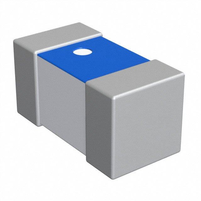
| 产品图片 |
|
| 产品型号 | DSS5140U-7 |
| rohs | 无铅 / 符合限制有害物质指令(RoHS)规范要求 |
| RoHS指令信息 | http://diodes.com/download/4349 |
| 产品系列 | - |
| 不同 Ib、Ic时的 Vce饱和值(最大值) | 500mV @ 100mA,1A |
| 不同 Ic、Vce 时的DC电流增益(hFE)(最小值) | 300 @ 100mA,5V |
| 产品目录页面 | |
| 供应商器件封装 | SOT-323 |
| 其它名称 | DSS5140U7 |
| 功率-最大值 | 400mW |
| 包装 | 带卷 (TR) |
| 安装类型 | 表面贴装 |
| 封装/外壳 | SC-70,SOT-323 |
| 晶体管类型 | PNP |
| 标准包装 | 3,000 |
| 电压-集射极击穿(最大值) | 40V |
| 电流-集电极(Ic)(最大值) | 1A |
| 电流-集电极截止(最大值) | 100nA |
| 频率-跃迁 | 150MHz |


- 商务部:美国ITC正式对集成电路等产品启动337调查
- 曝三星4nm工艺存在良率问题 高通将骁龙8 Gen1或转产台积电
- 太阳诱电将投资9.5亿元在常州建新厂生产MLCC 预计2023年完工
- 英特尔发布欧洲新工厂建设计划 深化IDM 2.0 战略
- 台积电先进制程称霸业界 有大客户加持明年业绩稳了
- 达到5530亿美元!SIA预计今年全球半导体销售额将创下新高
- 英特尔拟将自动驾驶子公司Mobileye上市 估值或超500亿美元
- 三星加码芯片和SET,合并消费电子和移动部门,撤换高东真等 CEO
- 三星电子宣布重大人事变动 还合并消费电子和移动部门
- 海关总署:前11个月进口集成电路产品价值2.52万亿元 增长14.8%


PDF Datasheet 数据手册内容提取
DSS5140U 40V PNP LOW SATURATION TRANSISTOR IN SOT323 Features Mechanical Data BVCEO > -40V Case: SOT323 IC = -1A Continuous Collector Current Case Material: Molded Plastic, “Green” Molding Compound. ICM = -2A Peak Pulse Current UL Flammability Classification Rating 94V-0 Low Saturation Voltage VCE(sat) < -500mV @ IC = -1A Moisture Sensitivity: Level 1 per J-STD-020 Ultra-Small Surface Mount Package Terminals: Finish — Matte Tin Plated leads. Solderable per Complementary NPN Type: DSS4140U MIL-STD-202, Method 208 e3 Totally Lead-Free & Fully RoHS Compliant (Notes 1 & 2) Weight: 0.006 grams (Approximate) Halogen and Antimony Free. “Green” Device (Note 3) Qualified to AEC-Q101 Standards for High Reliability SOT323 C B E Top View Top View Pin-Out Device Symbol Ordering Information (Note 4) Device Compliance Marking Reel Size (inches) Tape Width (mm) Quantity per reel DSS5140U-7 AEC-Q101 ZP6 7 8 3,000 Notes: 1. No purposely added lead. Fully EU Directive 2002/95/EC (RoHS) & 2011/65/EU (RoHS 2) compliant. 2. See http://www.diodes.com/quality/lead_free.html for more information about Diodes Incorporated’s definitions of Halogen- and Antimony-free, "Green" and Lead-free. 3. Halogen- and Antimony-free "Green” products are defined as those which contain <900ppm bromine, <900ppm chlorine (<1500ppm total Br + Cl) and <1000ppm antimony compounds. 4. For packaging details, go to our website at http://www.diodes.com/products/packages.html. Marking Information ZP6 = Product Type Marking Code ZP6 M YM = Date Code Marking Y Y = Year (ex: A = 2013) M = Month (ex: 9 = September) Date Code Key Year 2010 2011 2012 2013 2014 2015 2016 2017 2018 2019 2020 Code X Y Z A B C D E F G H Month Jan Feb Mar Apr May Jun Jul Aug Sep Oct Nov Dec Code 1 2 3 4 5 6 7 8 9 O N D DSS5140U 1 of 7 October 2014 Document number: DS31690 Rev. 3 - 2 www.diodes.com © Diodes Incorporated
DSS5140U Absolute Maximum Ratings (@TA = +25°C, unless otherwise specified.) Characteristic Symbol Value Unit Collector-Base Voltage VCBO -40 V Collector-Emitter Voltage VCEO -40 V Emitter-Base Voltage VEBO -5 V Collector Current - Continuous IC -1 A Peak Pulse Collector Current ICM -2 A Peak Base Current IBM -1 A Thermal Characteristics (@TA = +25°C, unless otherwise specified.) Characteristic Symbol Value Unit (Note 5) 400 Power Dissipation (Note 6) PD 500 mW (Note 5) 313 Thermal Resistance, Junction to Ambient (Note 6) RJA 250 °C/W Thermal Resistance, Junction to Leads (Note 7) RJL 350 °C/W Operating and Storage Temperature Range TJ, TSTG -55 to +150 °C ESD Ratings (Note 8) Characteristic Symbol Value Unit JEDEC Class Electrostatic Discharge - Human Body Model ESD HBM 4,000 V 3A Electrostatic Discharge - Machine Model ESD MM 400 V C Notes: 5. For a device mounted with collector lead on minimum recommended pad layout 1oz copper that is on a single-sided 1.6mm FR4 PCB; device is measured under still air conditions whilst operating in a steady-state. 6. Same as Note 5, except the collector lead is on a 25mm x 25mm 1oz copper. 7. Thermal resistance from junction to solder-point (at the end of the leads). 8. Refer to JEDEC specification JESD22-A114 and JESD22-A115. DSS5140U 2 of 7 October 2014 Document number: DS31690 Rev. 3 - 2 www.diodes.com © Diodes Incorporated
DSS5140U Thermal Characteristics and Derating Information 600 10 Pw = 1ms 500 mW) T (A) 1 Pw = 10ms ON ( 400 REN TI R A U P C SI 300 R 0.1 DIS TO Pw = 100ms R C E E DC W 200 LL O O P C 0.01 , D , C P 100 RJA = 313°C/W -I 0 0.001 0 25 50 75 100 125 150 0.1 1 10 100 TA, AMBIENT TEMPERATURE (°C) -VCE, COLLECTOR-EMITTER VOLTAGE (V) Fig. 2 Typical Collector Current Fig. 1 Power Dissipation vs. Ambient Temperature (Note 3) vs. Collector-Emitter Voltage (Note 3) 1 E D = 0.7 C N D = 0.5 A ST D = 0.3 SI E R 0.1 L D = 0.1 A M R D = 0.05 HE D = 0.9 RJA(t) = r(t) * RJA T T D = 0.02 RJA = 272°C/W N E 0.01 P(pk) NSI D = 0.01 t1 RA D = 0.005 t2 T TJ - TA = P * RJA(t) (t), Duty Cycle, D = t1/t2 r D = Single Pulse 0.001 0.00001 0.0001 0.001 0.01 0.1 1 10 100 1,000 10,000 t, PULSE DURATION TIME (s) 1 Fig. 3 Transient Thermal Response (Note 3) DSS5140U 3 of 7 October 2014 Document number: DS31690 Rev. 3 - 2 www.diodes.com © Diodes Incorporated
DSS5140U Electrical Characteristics (@TA = +25°C, unless otherwise specified.) Characteristic Symbol Min Typ Max Unit Test Condition OFF CHARACTERISTICS Collector-Base Breakdown Voltage BVCBO -40 V IC = -100µA, IE = 0 Collector-Emitter Breakdown Voltage (Note 9) BVCEO -40 V IC = -10mA, IB = 0 Emitter-Base Breakdown Voltage BVEBO -5 V IE = -100µA, IC = 0 Collector Cutoff Current ICBO --15000 nµAA VVCCBB == --4400VV,, IIEE == 00 , TJ = +150°C Collector Cutoff Current ICES -100 nA VCE = -40V, VBE = 0 Emitter Cutoff Current IEBO -100 nA VEB = -5V, IC = 0 ON CHARACTERISTICS (Note 9) 300 VCE = -5V, IC = -1mA DC Current Gain hFE 320500 800 VVCCEE == --55VV,, IICC == --150000mmAA 160 VCE = -5V, IC = 1A -200 IC = -100mA, IB = -1mA Collector-Emitter Saturation Voltage VCE(SAT) -250 mV IC = -500mA, IB = -50mA -500 IC = -1A, IB = -100mA Collector-Emitter Saturation Resistance RCE(SAT) 500 mΩ IC = -500mA, IB = -50mA Base-Emitter Saturation Voltage VBE(SAT) -1.1 V IC = -1A, IB = -50mA Base-Emitter Turn On Voltage VBE(ON) -1 V VCE = -5V, IC = -1A SMALL SIGNAL CHARACTERISTICS Output Capacitance Cobo 13 pF VCB = -10V, f = 1.0MHz Current Gain-Bandwidth Product fT 150 MHz VCE = -10V, IC = -50mA, f = 100MHz SWITCHING CHARACTERISTICS Turn-On Time ton 60 ns Delay Time td 25 ns Rise Time tr 35 ns VCC = -10V Turn-Off Time toff 250 ns IC = -0.5A, IB1 = -IB2 = -25mA Storage Time ts 220 ns Fall Time tf 30 ns Note: 9. Measured under pulsed conditions. Pulse width ≤ 300µs. Duty cycle ≤ 2%. DSS5140U 4 of 7 October 2014 Document number: DS31690 Rev. 3 - 2 www.diodes.com © Diodes Incorporated
DSS5140U Typical Electrical Characteristics (@TA = +25°C, unless otherwise specified.) 1,000 VCE = -5V 800 TA = 150°C N AI T G 600 TA = 85°C N E R R U TA = 25°C C 400 C D ,E F h 200 TA = -55°C 0 1 10 100 1,000 -I , COLLECTOR CURRENT (mA) C Fig. 4 Typical DC Current Gain vs. Collector Current V) 1.2 E ( G TA 1.0 IC/IB = 10 L O V N O 0.8 TI A R TA = -55°C U T 0.6 A R S TA = 25°C E T 0.4 T MI TA = 85°C E E- S 0.2 TA = 150°C A B , T) A 0 S E( 0.1 1 10 100 1,000 B V -I , COLLECTOR CURRENT (mA) - C Fig. 7 Typical Base-Emitter Saturation Voltage vs. Collector Current 1,000 f = 1MHz pF) 100 E ( C N Cibo A T CI A P A C 10 Cobo 1 0.1 1 10 100 V , REVERSE VOLTAGE (V) R Fig. 8 Typical Capacitance Characteristics DSS5140U 5 of 7 October 2014 Document number: DS31690 Rev. 3 - 2 www.diodes.com © Diodes Incorporated
DSS5140U Package Outline Dimensions Please see AP02002 at http://www.diodes.com/datasheets/ap02002.pdf for the latest version. H SOT323 Dim Min Max Typ K A 0.25 0.40 0.30 B 1.15 1.35 1.30 M a C 2.00 2.20 2.10 J D L D 0.650 BSC A F 0.375 0.475 0.425 G 1.20 1.40 1.30 H 1.80 2.20 2.15 J 0.00 0.10 0.05 K 0.90 1.00 0.95 C B L 0.25 0.40 0.30 M 0.10 0.18 0.11 a 8°C All Dimensions in mm G Suggested Pad Layout Please see AP02001 at http://www.diodes.com/datasheets/ap02001.pdf for the latest version. Y Dimensions SOT323 Z 2.8 Z C X 0.7 Y 0.9 C 1.9 E 1.0 X E DSS5140U 6 of 7 October 2014 Document number: DS31690 Rev. 3 - 2 www.diodes.com © Diodes Incorporated
DSS5140U IMPORTANT NOTICE DIODES INCORPORATED MAKES NO WARRANTY OF ANY KIND, EXPRESS OR IMPLIED, WITH REGARDS TO THIS DOCUMENT, INCLUDING, BUT NOT LIMITED TO, THE IMPLIED WARRANTIES OF MERCHANTABILITY AND FITNESS FOR A PARTICULAR PURPOSE (AND THEIR EQUIVALENTS UNDER THE LAWS OF ANY JURISDICTION). Diodes Incorporated and its subsidiaries reserve the right to make modifications, enhancements, improvements, corrections or other changes without further notice to this document and any product described herein. Diodes Incorporated does not assume any liability arising out of the application or use of this document or any product described herein; neither does Diodes Incorporated convey any license under its patent or trademark rights, nor the rights of others. Any Customer or user of this document or products described herein in such applications shall assume all risks of such use and will agree to hold Diodes Incorporated and all the companies whose products are represented on Diodes Incorporated website, harmless against all damages. Diodes Incorporated does not warrant or accept any liability whatsoever in respect of any products purchased through unauthorized sales channel. Should Customers purchase or use Diodes Incorporated products for any unintended or unauthorized application, Customers shall indemnify and hold Diodes Incorporated and its representatives harmless against all claims, damages, expenses, and attorney fees arising out of, directly or indirectly, any claim of personal injury or death associated with such unintended or unauthorized application. Products described herein may be covered by one or more United States, international or foreign patents pending. Product names and markings noted herein may also be covered by one or more United States, international or foreign trademarks. This document is written in English but may be translated into multiple languages for reference. Only the English version of this document is the final and determinative format released by Diodes Incorporated. LIFE SUPPORT Diodes Incorporated products are specifically not authorized for use as critical components in life support devices or systems without the express written approval of the Chief Executive Officer of Diodes Incorporated. As used herein: A. Life support devices or systems are devices or systems which: 1. are intended to implant into the body, or 2. support or sustain life and whose failure to perform when properly used in accordance with instructions for use provided in the labeling can be reasonably expected to result in significant injury to the user. B. A critical component is any component in a life support device or system whose failure to perform can be reasonably expected to cause the failure of the life support device or to affect its safety or effectiveness. Customers represent that they have all necessary expertise in the safety and regulatory ramifications of their life support devices or systems, and acknowledge and agree that they are solely responsible for all legal, regulatory and safety-related requirements concerning their products and any use of Diodes Incorporated products in such safety-critical, life support devices or systems, notwithstanding any devices- or systems-related information or support that may be provided by Diodes Incorporated. Further, Customers must fully indemnify Diodes Incorporated and its representatives against any damages arising out of the use of Diodes Incorporated products in such safety-critical, life support devices or systems. Copyright © 2014, Diodes Incorporated www.diodes.com DSS5140U 7 of 7 October 2014 Document number: DS31690 Rev. 3 - 2 www.diodes.com © Diodes Incorporated
Mouser Electronics Authorized Distributor Click to View Pricing, Inventory, Delivery & Lifecycle Information: D iodes Incorporated: DSS5140U-7