ICGOO在线商城 > 集成电路(IC) > PMIC - 监控器 > DS1706RESA+

 Datasheet下载
- 型号: DS1706RESA+
- 制造商: Maxim
- 库位|库存: xxxx|xxxx
- 要求:
| 数量阶梯 | 香港交货 | 国内含税 |
| +xxxx | $xxxx | ¥xxxx |
查看当月历史价格
查看今年历史价格
DS1706RESA+产品简介:
ICGOO电子元器件商城为您提供DS1706RESA+由Maxim设计生产,在icgoo商城现货销售,并且可以通过原厂、代理商等渠道进行代购。 DS1706RESA+价格参考。MaximDS1706RESA+封装/规格:PMIC - 监控器, 推挽式,图腾柱 监控器 1 通道 8-SOIC。您可以下载DS1706RESA+参考资料、Datasheet数据手册功能说明书,资料中有DS1706RESA+ 详细功能的应用电路图电压和使用方法及教程。
Maxim Integrated(现为Analog Devices旗下品牌)的DS1706RESA+是一款电压监控器(Voltage Monitor),属于PMIC(电源管理集成电路)中的监控器类别。该芯片主要用于监测电源电压的稳定性,确保系统在电压异常时能够及时做出反应,常用于需要高可靠性的电子系统中。

应用场景包括:

1. 工业控制系统:用于监测工业设备的电源电压,防止因电压过低或波动导致设备误动作或损坏。

2. 通信设备:在路由器、交换机等通信设备中,确保系统在电源异常时能及时复位或告警,提高系统稳定性。

3. 嵌入式系统与单片机系统:为嵌入式控制器提供电源监控功能,保障系统在电压不足时不执行错误操作。

4. 消费电子产品:如智能家电、智能仪表等,用于监测主电源或电池电压,防止低电压运行造成数据丢失或硬件损坏。

5. 汽车电子:在车载电子系统中用于监控电池或电源模块电压,保障汽车电子设备的正常运行。

DS1706RESA+具有低功耗、精准电压检测阈值和手动复位功能,适用于多种对电源监控有较高要求的应用场景。
| 参数 | 数值 |
| 产品目录 | 集成电路 (IC)半导体 |
| 描述 | IC MICROMONITOR 3.3V 20% 8-SOIC监控电路 3.3/5V MicroMonitor |
| 产品分类 | |
| 品牌 | Maxim Integrated |
| 产品手册 | |
| 产品图片 |
|
| rohs | 符合RoHS无铅 / 符合限制有害物质指令(RoHS)规范要求 |
| 产品系列 | 电源管理 IC,监控电路,Maxim Integrated DS1706RESA+MicroMonitor™ |
| NumberofInputsMonitored | 1 Input |
| 数据手册 | |
| 产品型号 | DS1706RESA+ |
| 产品培训模块 | http://www.digikey.cn/PTM/IndividualPTM.page?site=cn&lang=zhs&ptm=25703http://www.digikey.cn/PTM/IndividualPTM.page?site=cn&lang=zhs&ptm=25705 |
| 产品种类 | 监控电路 |
| 人工复位 | Manual Reset |
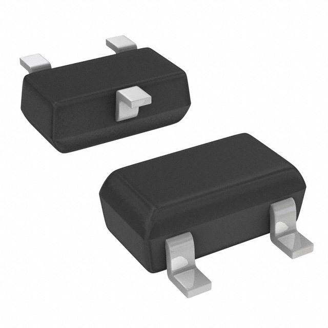
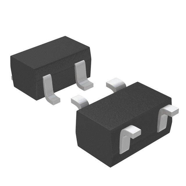
| 供应商器件封装 | 8-SOIC N |
| 功率失效检测 | Yes |
| 包装 | 管件 |
| 受监控电压数 | 1 |
| 商标 | Maxim Integrated |
| 复位 | 低有效 |
| 复位超时 | 最小为 130 ms |
| 安装类型 | 表面贴装 |
| 封装 | Tube |
| 封装/外壳 | 8-SOIC(0.154",3.90mm 宽) |
| 封装/箱体 | SOIC-8 |
| 工作温度 | -40°C ~ 85°C |
| 工作电源电流 | 60 uA |
| 工厂包装数量 | 100 |
| 应用说明 | |
| 最大工作温度 | + 85 C |
| 最小工作温度 | - 40 C |
| 标准包装 | 100 |
| 欠电压阈值 | 2.55 V |
| 电压-阈值 | 2.63V |
| 电池备用开关 | No Backup |
| 电源电压-最大 | 5.5 V |
| 电源电压-最小 | 1.2 V |
| 监视器 | Watchdog |
| 类型 | Voltage Supervisory |
| 系列 | DS1706R |
| 芯片启用信号 | No Chip Enable |
| 被监测输入数 | 1 Input |
| 输出 | 推挽式,图腾柱 |
| 输出类型 | Active Low, Push-Pull |
| 过电压阈值 | 2.7 V |
| 重置延迟时间 | 285 ms |
| 阈值电压 | 3.3 V, 5 V |
| 零件号别名 | 90-1706R+S00 DS1706R |


- 商务部:美国ITC正式对集成电路等产品启动337调查
- 曝三星4nm工艺存在良率问题 高通将骁龙8 Gen1或转产台积电
- 太阳诱电将投资9.5亿元在常州建新厂生产MLCC 预计2023年完工
- 英特尔发布欧洲新工厂建设计划 深化IDM 2.0 战略
- 台积电先进制程称霸业界 有大客户加持明年业绩稳了
- 达到5530亿美元!SIA预计今年全球半导体销售额将创下新高
- 英特尔拟将自动驾驶子公司Mobileye上市 估值或超500亿美元
- 三星加码芯片和SET,合并消费电子和移动部门,撤换高东真等 CEO
- 三星电子宣布重大人事变动 还合并消费电子和移动部门
- 海关总署:前11个月进口集成电路产品价值2.52万亿元 增长14.8%


PDF Datasheet 数据手册内容提取
19-5212; Rev 4/10 DS1705/DS1706 3.3V and 5.0V MicroMonitor www.maxim-ic.com FEATURES PIN ASSIGNMENT Halts and restarts an out-of-control microprocessor PBRST 1 8 WDS Holds microprocessor in check during power V 2 7 RST CC transients GND 3 6 ST Automatically restarts microprocessor after IN 4 5 NMI power failure 8-Pin DIP (300 -mil) Monitors pushbutton for external override Accurate 5%, 10% or 20% resets for 3.3V PBRST 1 8 WDS systems and 5% or 10% resets for 5.0V V 2 7 RST(*RST) systems CC Eliminates the need for discrete components GND 3 6 ST 3.3V 20% tolerance for use with 3.0V IN 4 5 NMI systems 8-Pin SOIC (150-mil) Pin-compatible with the MAXIM RST(*RST) 1 8 ST MAX705/MAX706 in 8-pin DIP, 8-pin SOIC, WDS 2 7 NMI and -SOP PBRST 3 6 IN 8-pin DIP, 8-pin SOIC and 8-pin -SOP VCC 4 5 GND packages 8-Pin -SOP (118-mil) See Mech. Drawings Section on website Industrial temperature range -40C to +85C DS1705 and DS1706_R/S/T (*DS1706L and DS1706P) PIN DESCRIPTION PBRST - Pushbutton Reset Input V - Power Supply CC GND - Ground IN - Input NMI - Non-maskable Interrupt ST - Strobe Input RST - Active Low Reset Output *RST - Active High Reset Output (DS1706P and DS1706L only) WDS - Watchdog Status Output DESCRIPTION The DS1705/DS1706 3.3- or 5.0-Volt MicroMonitor monitors three vital conditions for a microprocessor: power supply, software execution, and external override. A precision temperature compensated reference and comparator circuit monitor the status of V at the device and at an upstream point for maximum CC protection. When the sense input detects an out-of-tolerance condition, a non-maskable interrupt is generated. As the voltage at the device degrades, an internal power fail signal is generated which forces 1 of 12
DS1705/DS1706 the reset to an active state. When V returns to an in-tolerance condition, the reset signal is kept in the CC active state for a minimum of 130 ms to allow the power supply and processor to stabilize. The second function the DS1705/DS1706 performs is pushbutton reset control. The DS1705/DS1706 debounces the pushbutton input and guarantees an active reset pulse width of 130 ms minimum. The third function is a watchdog timer. The DS1705/DS1706 has an internal timer that forces the WDS output signal to the active state if the strobe input is not driven low prior to time-out. OPERATION Power Monitor The DS1705/DS1706 detects out-of-tolerance power supply conditions and warns a processor-based system of impending power failure. When V falls below the minimum V tolerance, a comparator CC CC outputs the RST (or RST) signal. RST (or RST) is an excellent control signal for a microprocessor, as processing is stopped at the last possible moment of valid V . On power-up, RST (or RST) are kept CC active for a minimum of 130 ms to allow the power supply and processor to stabilize. Pushbutton Reset The DS1705/DS1706 provides an input pin for direct connection to a pushbutton reset (see Figure 2). The pushbutton reset input requires an active low signal. Internally, this input is debounced and timed such that a RST (or RST) signal of at least 130 ms minimum will be generated. The 130 ms delay commences as the pushbutton reset input is released from the low level. The pushbutton can be initiated by connecting the WDS or NMI outputs to the PBRST input as shown in Figure 3. Non-Maskable Interrupt The DS1705/DS1706 generates a non-maskable interrupt (NMI) for early warning of a power failure. A precision comparator monitors the voltage level at the IN pin relative to an on-chip reference generated by an internal band gap. The IN pin is a high impedance input allowing for a user-defined sense point. An external resistor voltage divider network (Figure 5) is used to interface with high voltage signals. This sense point may be derived from a regulated supply or from a higher DC voltage level closer to the main system power input. Since the IN trip point V is 1.25 volts, the proper values for R1 and R2 can be TP determined by the equation as shown in Figure 5. Proper operation of the DS1705/DS1706 requires that the voltage at the IN pin be limited to V . Therefore, the maximum allowable voltage at the supply being CC monitored (V ) can also be derived as shown in Figure 5. A simple approach to solving the equation is MAX to select a value for R2 high enough to keep power consumption low, and solve for R1. The flexibility of the IN input pin allows for detection of power loss at the earliest point in a power supply system, maximizing the amount of time for system shutdown between NMI and RST (or RST). When the supply being monitored decays to the voltage sense point, the DS1705/DS1706 pulses the NMI output to the active state for a minimum 200 s. The NMI power-fail detection circuitry also has built-in hysteresis of 100 V. The supply must be below the voltage sense point for approximately 5 s before a low NMI will be generated. In this way, power supply noise is removed from the monitoring function, preventing false interrupts. During a power-up, any detected IN pin levels below V by the comparator TP are disabled from generating an interrupt until V rises to V . As a result, any potential NMI pulse CC CCTP will not be initiated until V reaches V . CC CCTP Connecting NMI to PBRST would allow non-maskable interrupt to generate an automatic reset when an out-of-tolerance condition occurred in a monitored supply. An example is shown in Figure 3. 2 of 12
DS1705/DS1706 Watchdog Timer The watchdog timer function forces WDS signals active when the ST input is not clocked within the 1 second time-out period. Time-out of the watchdog starts when RST (or RST) becomes inactive. If a high- to-low transition occurs on the ST input pin prior to time-out, the watchdog timer is reset and begins to time out again. If the watchdog timer is allowed to time out, the WDS signal is driven active (low) for a minimum of 130 ms. The ST input can be derived from many microprocessor outputs. The typical signals used are the microprocessors address signals, data signals, or control signals. When the microprocessor functions normally, these signals would, as a matter of routine, cause the watchdog to be reset prior to time-out. To guarantee that the watchdog timer does not time out, a high-to-low transition must occur at or less than the minimum watchdog time-out of 1 second. A typical circuit example is shown in Figure 6. MICROMONITOR BLOCK DIAGRAM Figure 1 40k 180k PUSH-BUTTON RESET Figure 2 3 of 12
DS1705/DS1706 PUSH-BUTTON RESET CONTROLLED BY NMI AND WDS Figure 3 TIMING DIAGRAM: PUSHBUTTON RESET Figure 4 NON-MASKABLE INTERRUPT CIRCUIT EXAMPLE Figure 5 R1 R2 V SENSE V = X 1.25 V = X V SENSE MAX CC R2 V TP Example: V = 4.50V at the trip point SENSE V = 3.3V CC 10 kΩ = R2 4.50 Therefore: X 3.3 = 11.88V maximum 1.25 R1 10k 4.5 = X 1.25 R1 = 26 kΩ 10k 4 of 12
DS1705/DS1706 WATCHDOG TIMER Figure 6 TIMING DIAGRAM: STROBE INPUT Figure 7 TIMING DIAGRAM: NON-MASKABLE INTERRUPT Figure 8 5 of 12
DS1705/DS1706 TIMING DIAGRAM: POWER-DOWN Figure 9 6 of 12
DS1705/DS1706 TIMING DIAGRAM: POWER-UP Figure 10 7 of 12
DS1705/DS1706 ABSOLUTE MAXIMUM RATINGS Voltage Range on V Pin Relative to Ground -0.5V to +7.0V CC Voltage Range on I/O Relative to Ground* -0.5V to (V + 0.5V) CC Operating Temperature Range -40C to +85C Storage Temperature Range -55C to +125C Lead Temperature (soldering, 10s) +260C Soldering Temperature (reflow) Lead(Pb)-free +260C Containing lead(Pb) +240C This is a stress rating only and functional operation of the device at these or any other conditions above those indicated in the operation sections of this specification is not implied. Exposure to absolute maximum rating conditions for extended periods of time may affect reliability. *The voltage input on IN, ST, and PBRST can be exceeded if the input current is less than 10 mA. RECOMMENDED DC OPERATING CONDITIONS (T = -40C to +85C) A PARAMETER SYMBOL MIN TYP MAX UNITS NOTES Supply Voltage V 1.2 5.5 V 1 CC ST and PBRST Input High Level VIH 2.0 VCC+0.3 V 1, 3 V -0.5 1, 4 CC ST and PBRST Input Low Level VIL -0.03 +0.5 V 1 DC ELECTRICAL CHARACTERISTICS (V = 1.2V to 5.5V, T = -40C to +85C.) CC A PARAMETER SYMBOL MIN TYP MAX UNITS NOTES V Trip Point DS1705/DS1706L V 4.50 4.65 4.75 V 1 CC CCTP V Trip Point DS1706 V 4.25 4.40 4.50 V 1 CC CCTP V Trip Point DS1706T V 3.00 3.08 3.15 V 1 CC CCTP V Trip Point DS1706S V 2.85 2.93 3.00 V 1 CC CCTP V Trip Point DS1706P or R V 2.55 2.63 2.70 V 1 CC CCTP Input Leakage I -1.0 +1.0 A 2 IL Output Current @ 2.4V I 350 A 3 OH Output Current @ 0.4V I 10 mA 3 OL Output Voltage @ -500 A V V -0.3 V -0.1 V 3 OH CC CC Operating Current I 60 A 5 CC @ V < 5.5V CC Operating Current I 50 A 5 CC @ V < 3.6V CC IN Input Trip Point V 1.20 1.25 1.30 V 1 TP CAPACITANCE (T = +25C) A PARAMETER SYMBOL MIN TYP MAX UNITS NOTES Input Capacitance C 5 pF IN Output Capacitance C 7 pF OUT 8 of 12
DS1705/DS1706 AC ELECTRICAL CHARACTERISTICS (V = 1.2V to 5.5V, T = -40C to +85C.) CC A PARAMETER SYMBOL MIN TYP MAX UNITS NOTES PBRST = VIL tPB 150 ns Reset Active Time t 130 205 285 ms RST ST Pulse Width tST 10 ns 6 VCC Detect to RST and RST tRPD 5 8 s 9 V Slew Rate t 20 s CC F VCC Detect to RST and RST tRPU 130 205 285 ms 7 V Slew Rate t 0 ns CC R PBRST Stable Low to RST and RST tPDLY 250 ns Watchdog Timeout t 1.0 1.6 2.2 s 8 TD VIN Detect to NMI tIPD 5 8 s 9 NOTES: 1. All voltages are referenced to ground. 2. PBRST is internally pulled up to V with an internal impedance of 40 ktypical and the ST input is CC internally pulled up to V with an internal impedance of 180 ktypical. CC 3. V ≥ 2.4V. CC 4. V < 2.4V. CC 5. Measured with outputs open and all inputs at V or ground. CC 6. Must not exceed t minimum. TD 7. t = 5 s. R 8. Minimum watchdog time-out tested at 2.7V for the 3.3V devices and 4.5V for the 5.0V devices. 9. Noise immunity pulses < 2 s will not cause a reset. 9 of 12
DS1705/DS1706 PART MARKING CODES DS170AB 8-pin DIP yywwrv cccccc (300 MIL) ###xx 8-pin SOIC DS170AB yywwrv (150 MIL) ###xx cccccc 8-pin µSOP 170AB (118 MIL) ywwrv ###xx BRAND CODES CODE DESCRIPTION VALUES AB Device type and tolerance 5_, 6_, 6L, 6P, 6R, 6S, 6T (where’_’ is a blank) yww or yyww Date Code. Identifies the year and work y, the last digit of the year. week the device was assembled. yy, the last two digits of the year. ww, the work week (values 01 through 52). rv Die Revision A letter followed by a number (eg. B1) ###xx Lot Code Three numbers followed by 2 letters cccccc Country of Assembly Abbreviation of country name. 10 of 12
DS1705/DS1706 ORDERING INFORMATION PART TEMP RANGE PIN-PACKAGE VERSION DS1705EPA -40°C to +85°C 8-pin PDIP (300 mils) 5V-5% MONITOR, /RST, /WDS DS1705ESA -40°C to +85°C 8-pin SO (150 mils) 5V-5% MONITOR, /RST, /WDS DS1705EUA -40°C to +85°C 8-pin µSOP (118 mils) 5V-5% MONITOR, /RST, /WDS DS1706EPA -40°C to +85°C 8-pin PDIP (300 mils) 5V-10% MONITOR, /RST, /WDS DS1706ESA -40°C to +85°C 8-pin SO (150 mils) 5V-10% MONITOR, /RST, /WDS DS1706EUA -40°C to +85°C 8-pin µSOP (118 mils) 5V-10% MONITOR, /RST, /WDS DS1706LEPA -40°C to +85°C 8-pin PDIP (300 mils) 5V-5% MONITOR, RST, /WDS DS1706LESA -40°C to +85°C 8-pin SO (150 mils) 5V-5% MONITOR, RST, /WDS DS1706LEUA -40°C to +85°C 8-pin µSOP (118 mils) 5V-5% MONITOR, RST, /WDS DS1706PEPA -40°C to +85°C 8-pin PDIP (300 mils) 3.3V-20% MONITOR, RST, /WDS DS1706PESA -40°C to +85°C 8-pin SO (150 mils) 3.3V-20% MONITOR, RST, /WDS DS1706PEUA -40°C to +85°C 8-pin µSOP (118 mils) 3.3V-20% MONITOR, RST, /WDS DS1706REPA -40°C to +85°C 8-pin PDIP (300 mils) 3.3V-20% MONITOR, /RST, /WDS DS1706RESA -40°C to +85°C 8-pin SO (150 mils) 3.3V-20% MONITOR, /RST, /WDS DS1706REUA -40°C to +85°C 8-pin µSOP (118 mils) 3.3V-20% MONITOR, /RST, /WDS DS1706SEPA -40°C to +85°C 8-pin PDIP (300 mils) 3.3V-10% MONITOR, /RST, /WDS DS1706SESA -40°C to +85°C 8-pin SO (150 mils) 3.3V-10% MONITOR, /RST, /WDS DS1706SEUA -40°C to +85°C 8-pin µSOP (118 mils) 3.3V-10% MONITOR, /RST, /WDS DS1706TEPA -40°C to +85°C 8-pin PDIP (300 mils) 3.3V-5% MONITOR, /RST, /WDS DS1706TESA -40°C to +85°C 8-pin SO (150 mils) 3.3V-5% MONITOR, /RST, /WDS DS1706TEUA -40°C to +85°C 8-pin µSOP (118 mils) 3.3V-5% MONITOR, /RST, /WDS Note: Devices are also available in a lead(Pb)-free/RoHS-compliant package. Specify lead-free by adding a plus (+) to the part number when ordering. E = -40°C to +85°C temperature range A = 8-lead device P = Plastic DIP (300 mils) S = SO (150 mils) U = µSOP (118 mils) PACKAGE INFORMATION For the latest package outline information and land patterns, go to www.maxim-ic.com/packages. Note that a “+”, “#”, or “-” in the package code indicates RoHS status only. Package drawings may show a different suffix character, but the drawing pertains to the package regardless of RoHS status. PACKAGE TYPE PACKAGE CODE DOCUMENT NO. 8 PDIP P8-2 21-0043 8 SO S8-2 21-0041 8 SOP U8-1 21-0036 11 of 12
DS1705/DS1706 REVISION HISTORY REVISION PAGES DESCRIPTION DATE CHANGED Added the lead temperature and updated the soldering 4/10 8, 9 temperature in the Absolute Maximum Ratings; corrected Note 9. 12 of 12 Maxim cannot assume responsibility for use of any circuitry other than circuitry entirely embodied in a Maxim product. No circuit patent licenses are implied. Maxim reserves the right to change the circuitry and specifications without notice at any time. Maxim Integrated Products, 120 San Gabriel Drive, Sunnyvale, CA 94086 408-737-7600 © 2010 Maxim Integrated Products Maxim is a registered trademark of Maxim Integrated Products, Inc. The Dallas logo is a registered trademark of Maxim Integrated Products, Inc.
Mouser Electronics Authorized Distributor Click to View Pricing, Inventory, Delivery & Lifecycle Information: M axim Integrated: DS1706EUA+ DS1705EPA+ DS1705ESA+ DS1705ESA+T&R DS1706ESA+ DS1706LEPA+ DS1706LESA+ DS1706LESA+T&R DS1706RESA+ DS1706SESA+ DS1706TESA+ DS1705EPA DS1705ESA DS1705EUA+ DS1705EUA+T&R DS1706EPA DS1706EPA+ DS1706ESA+T&R DS1706EUA+T&R DS1706LEPA DS1706LEUA+ DS1706LEUA+T&R DS1706PEPA DS1706PEPA+ DS1706PESA+ DS1706PESA+T&R DS1706PEUA+ DS1706PEUA+T&R DS1706REPA+ DS1706RESA+T&R DS1706REUA+ DS1706REUA+T&R DS1706SEPA+ DS1706SESA+T&R DS1706SEUA+ DS1706SEUA+T&R DS1706TEPA+ DS1706TESA DS1706TESA+T&R DS1706TEUA+ DS1706TEUA+T&R