ICGOO在线商城 > 集成电路(IC) > 逻辑 - 信号开关,多路复用器,解码器 > DS10CP154ATSQ/NOPB

 Datasheet下载
- 型号: DS10CP154ATSQ/NOPB
- 制造商: Texas Instruments
- 库位|库存: xxxx|xxxx
- 要求:
| 数量阶梯 | 香港交货 | 国内含税 |
| +xxxx | $xxxx | ¥xxxx |
查看当月历史价格
查看今年历史价格
DS10CP154ATSQ/NOPB产品简介:
ICGOO电子元器件商城为您提供DS10CP154ATSQ/NOPB由Texas Instruments设计生产,在icgoo商城现货销售,并且可以通过原厂、代理商等渠道进行代购。 DS10CP154ATSQ/NOPB价格参考¥34.89-¥58.75。Texas InstrumentsDS10CP154ATSQ/NOPB封装/规格:逻辑 - 信号开关,多路复用器,解码器, Crosspoint Switch 1 x 4:4 40-WQFN (6x6)。您可以下载DS10CP154ATSQ/NOPB参考资料、Datasheet数据手册功能说明书,资料中有DS10CP154ATSQ/NOPB 详细功能的应用电路图电压和使用方法及教程。
Texas Instruments 的 DS10CP154ATSQ/NOPB 是一款高速信号开关/多路复用器,主要应用于需要高频信号路由的通信和工业系统中。该器件属于逻辑类集成电路中的信号开关与多路复用器类别。

其典型应用场景包括:

1. 通信设备:用于高速数据通信系统中对差分信号进行切换或选择,如在背板、交换系统或光模块中实现信号路径的灵活控制。

2. 测试与测量仪器:在示波器、信号发生器等设备中作为高速信号选择开关,实现多个输入信号的快速切换与处理。

3. 工业控制系统:用于高精度工业自动化设备中,对传感器或多路信号源进行高效切换,提升系统集成度与响应速度。

4. 视频与广播设备:在高清视频传输系统中实现高速差分信号(如LVDS)的多路选择与传输。

该芯片支持高达3.2Gbps的数据速率,采用低电压差分信号(LVDS)技术,具有低功耗、低串扰和高信号完整性等优点,适用于高性能数字系统设计。
| 参数 | 数值 |
| 产品目录 | 集成电路 (IC)半导体 |
| 描述 | IC CROSSPOINT SWITCH 4X4 40LLP模拟和数字交叉点 IC Auto 1.5Gbps 4X4 LVDS Crosspt Switch |
| 产品分类 | |
| 品牌 | Texas Instruments |
| 产品手册 | |
| 产品图片 |
|
| rohs | 符合RoHS无铅 / 符合限制有害物质指令(RoHS)规范要求 |
| 产品系列 | 通信及网络 IC,模拟和数字交叉点 IC,Texas Instruments DS10CP154ATSQ/NOPB- |
| 数据手册 | |
| 产品型号 | DS10CP154ATSQ/NOPB |
| 产品 | LVDS Crosspoint Switch |
| 产品目录页面 | |
| 产品种类 | 模拟和数字交叉点 IC |
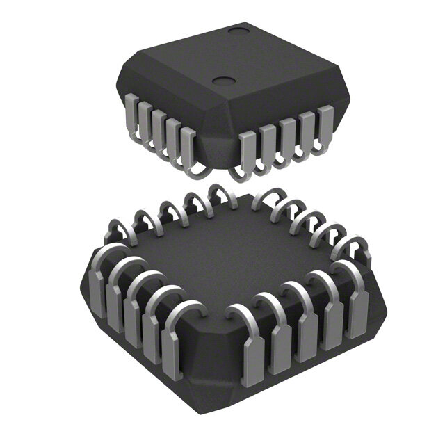
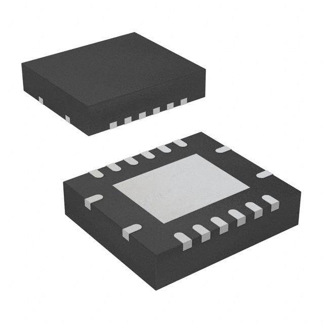
| 供应商器件封装 | 40-LLP-EP(6x6) |
| 其它名称 | DS10CP154ATSQ/NOPBDKR |
| 包装 | Digi-Reel® |
| 商标 | Texas Instruments |
| 安装类型 | 表面贴装 |
| 安装风格 | SMD/SMT |
| 封装 | Reel |
| 封装/外壳 | 40-WFQFN 裸露焊盘 |
| 封装/箱体 | WQFN-40 |
| 工作温度 | -40°C ~ 85°C |
| 工作电源电压 | 3.3 V |
| 工厂包装数量 | 250 |
| 数据速率 | 1.5 Gb/s |
| 最大工作温度 | + 85 C |
| 最小工作温度 | - 40 C |
| 标准包装 | 1 |
| 独立电路 | 1 |
| 电压-电源 | 3 V ~ 3.6 V |
| 电压源 | 单电源 |
| 电流-输出高,低 | - |
| 电源电压-最大 | 3.6 V |
| 电源电压-最小 | 3 V |
| 电源类型 | Digital |
| 电路 | 1 x 4:4 |
| 类型 | 交点开关 |
| 系列 | DS10CP154A |
| 输入电平 | LVDS, CML, LVPECL |
| 输出电平 | LDVS |
| 配置 | 4 x 4 |
| 阵列数量 | 1 |


- 商务部:美国ITC正式对集成电路等产品启动337调查
- 曝三星4nm工艺存在良率问题 高通将骁龙8 Gen1或转产台积电
- 太阳诱电将投资9.5亿元在常州建新厂生产MLCC 预计2023年完工
- 英特尔发布欧洲新工厂建设计划 深化IDM 2.0 战略
- 台积电先进制程称霸业界 有大客户加持明年业绩稳了
- 达到5530亿美元!SIA预计今年全球半导体销售额将创下新高
- 英特尔拟将自动驾驶子公司Mobileye上市 估值或超500亿美元
- 三星加码芯片和SET,合并消费电子和移动部门,撤换高东真等 CEO
- 三星电子宣布重大人事变动 还合并消费电子和移动部门
- 海关总署:前11个月进口集成电路产品价值2.52万亿元 增长14.8%


PDF Datasheet 数据手册内容提取
DS10CP154A www.ti.com SNLS306C–AUGUST2008–REVISEDAPRIL2013 DS10CP154A 1.5 Gbps 4x4 LVDS Crosspoint Switch CheckforSamples:DS10CP154A FEATURES DESCRIPTION 1 • DC-1.5GbpsLowJitter,LowSkew,Low The DS10CP154A is a 1.5 Gbps 4x4 LVDS crosspoint switch optimized for high-speed signal PowerOperation routing and switching over FR-4 printed circuit board • PinandSMBusConfigurable,Fully backplanes and balanced cables. Fully differential Differential,Non-BlockingArchitecture signal paths ensure exceptional signal integrity and • WideInputCommonModeRangeEnablesDC noise immunity. The non-blocking architecture allows CoupledInterfacetoCMLorLVPECLDrivers connections of any input to any output or outputs. The switch configuration can be accomplished via • LOSCircuitryDetectsOpenInputsFault external pins or the System Management Bus Condition (SMBus) interface. In addition, the SMBus circuitry • On-chip100Ω InputandOutputTermination enables the loss of signal (LOS) monitors that can MinimizesInsertionandReturnLosses, inform a system of the presence of an open inputs ReducesComponentCountandMinimizes condition(e.g.disconnectedcable). BoardSpace Wide input common mode range allows the switch to • 8kVESDonLVDSI/OPinsProtectsAdjoining accept signals with LVDS, CML and LVPECL levels; Components the output levels are LVDS. A very small package footprint requires a minimal space on the board while • Small6mmx6mmWQFN-40SpaceSaving the flow-through pinout allows easy board layout. Package Each differential input and output is internally terminated with a 100Ω resistor to lower return APPLICATIONS losses, reduce component count and further minimize • High-speedChannelSelectApplications boardspace. • ClockandDataBufferingandMuxing • SD/HDSDIRouters Typical Application INPUT CARD OUTPUT CARD AdaptSivDe /E HqDualizer BACKPLANES CRaeSbcDlleo /cD HkreDivr e+r AdaptSivDe /E HqDualizer DS10CP154 DS10CP154 CRaeSbcDlleo /cD HkreDivr e+r 4x4 LVDS 4x4 LVDS Crosspoint Switch Crosspoint Switch AdaptSivDe /E HqDualizer CRaeSbcDlleo /cD HkreDivr e+r AdaptSivDe /E HqDua lizer CRaeSbcDlleo /cD HkreDivr e+r DS10CP154 4x4 LVDS Crosspoint Switch CROSSPOINT CARD 1 Pleasebeawarethatanimportantnoticeconcerningavailability,standardwarranty,anduseincriticalapplicationsof TexasInstrumentssemiconductorproductsanddisclaimerstheretoappearsattheendofthisdatasheet. PRODUCTIONDATAinformationiscurrentasofpublicationdate. Copyright©2008–2013,TexasInstrumentsIncorporated Products conform to specifications per the terms of the Texas Instruments standard warranty. Production processing does not necessarilyincludetestingofallparameters.
DS10CP154A SNLS306C–AUGUST2008–REVISEDAPRIL2013 www.ti.com Block Diagram S00 – S31 8 IN0+ OUT0+ IN0- OUT0+ IN1+ OUT1+ IN1- OUT1- 4 X 4 IN2+ OUT2+ IN2- OUT2- IN3+ OUT3+ IN3- OUT3- System Management Bus PWDN 4 b A L n m D C R s S S D EN_ AD Connection Diagram 0 1 2 3 R R R R L A D D D D C C WDN 00/SC 01/SD 10/AD 11/AD 20/AD 21/AD C N N P S S S S S S N 0 9 8 7 6 5 4 3 2 1 4 3 3 3 3 3 3 3 3 3 IN0+ 1 30 VDD IN0- 2 29 OUT0+ VDD 3 28 OUT0- IN1+ 4 27 OUT1+ DAP IN1- 5 26 OUT1- IN2+ 6 (GND) 25 VDD IN2- 7 24 OUT2+ VDD 8 23 OUT2- IN3+ 9 22 OUT3+ IN3- 10 21 OUT3- 1 2 3 4 5 6 7 8 9 0 1 1 1 1 1 1 1 1 1 2 C C 0 1 D D b C C C N N S3 S3 VD GN _sm N N N N E Figure1. WQFNPackage SeePackageNumberRTA0040A 2 SubmitDocumentationFeedback Copyright©2008–2013,TexasInstrumentsIncorporated ProductFolderLinks:DS10CP154A
DS10CP154A www.ti.com SNLS306C–AUGUST2008–REVISEDAPRIL2013 PINDESCRIPTIONS Pin PinName I/O,Type PinDescription Number IN0+,IN0-, 1,2, I,LVDS Invertingandnon-invertinghighspeedLVDSinputpins. IN1+,IN1-, 4,5, IN2+,IN2-, 6,7, IN3+,IN3- 9,10 OUT0+,OUT0-, 29,28, O,LVDS Invertingandnon-invertinghighspeedLVDSoutputpins. OUT1+,OUT1-, 27,26, OUT2+,OUT2-, 24,23, OUT3+,OUT3- 22,21 EN_smb 17 I,LVCMOS SystemManagementBus(SMBus)modeenablepin.Thepinhasaninternal 20kpulldown.Whenthepinissettoa[1],thedeviceisintheSMBusmode. AllSMBusregistersareresetwhenthepinistoggled. S00/SCL, 37, I/O,LVCMOS ForEN_smb=[0],thesepinsselectwhichLVDSinputisroutedtotheOUT0. S01/SDA 36 IntheSMBusmode,whentheEN_smb=[1],thesepinsaretheSMBusclock inputanddataI/Opinsrespectively. S10/ADDR0, 35, I/O,LVCMOS ForEN_smb=[0],thesepinsselectwhichLVDSinputisroutedtotheOUT1. S11/ADDR1 34 IntheSMBusmode,whentheEN_smb=[1],thesepinsaretheUser-Set SMBusSlaveAddressinputs. S20/ADDR2, 33, I/O,LVCMOS ForEN_smb=[0],thesepinsselectwhichLVDSinputisroutedtotheOUT2. S21/ADDR3 32 IntheSMBusmode,whentheEN_smb=[1],thesepinsaretheUser-Set SMBusSlaveAddressinputs. S30,S31 13,14 I,LVCMOS ForEN_smb=[0],thesepinsselectwhichLVDSinputisroutedtotheOUT3. IntheSMBusmode,whentheEN_smb=[1],thesepinsarenon-functional andshouldbetiedtoeitherlogic[0]or[1]. PWDN 38 I,LVCMOS ForEN_smb=[0],thisisthepowerdownpin.WhenthePWDNissettoa[0], thedeviceisinthepowerdownmode.TheSMBuscircuitrycanstillbe accessedprovidedtheEN_smbpinissettoa[1]. IntheSMBusmode,thedeviceispoweredupbyeithersettingthePWDNpin to[1]ORbywritinga[1]totheControlRegisterD[7]bit(SoftPWDN).The devicewillbepowereddownbysettingthePWDNpinto[0]ANDbywritinga [0]totheControlRegisterD[7]bit(SoftPWDN). NC 11,12,18, Noconnectpins.Maybeleftfloating. 19,20,31, 39,40 VDD 3,8, Power Powersupplypins. 15,25,30 GND 16,DAP Power Groundpinandpad(DAP-dieattachpad). Copyright©2008–2013,TexasInstrumentsIncorporated SubmitDocumentationFeedback 3 ProductFolderLinks:DS10CP154A
DS10CP154A SNLS306C–AUGUST2008–REVISEDAPRIL2013 www.ti.com Absolute Maximum Ratings(1)(2) SupplyVoltage −0.3Vto+4V LVCMOSInputVoltage −0.3Vto(V +0.3V) CC LVCMOSOutputVoltage −0.3Vto(V +0.3V) CC LVDSInputVoltage −0.3Vto+4V DifferentialInputVoltage|VID| 1.0V LVDSOutputVoltage −0.3Vto(V +0.3V) CC LVDSDifferentialOutputVoltage 0Vto1.0V LVDSOutputShortCircuitCurrentDuration 5ms JunctionTemperature +150°C StorageTemperatureRange −65°Cto+150°C LeadTemperatureRange Soldering(4sec.) +260°C MaximumPackagePowerDissipationat RTA0040APackage 4.65W 25°C DerateRTA0040APackage 37.2mW/°Cabove+25°C PackageThermalResistance θ +26.9°C/W JA θ +3.8°C/W JC ESDSusceptibility HBM(3) ≥8kV MM(4) ≥250V CDM(5) ≥1250V (1) AbsoluteMaximumRatingsindicatelimitsbeyondwhichdamagetothedevicemayoccur,includinginoperabilityanddegradationof devicereliabilityand/orperformance.Functionaloperationofthedeviceand/ornon-degradationattheAbsoluteMaximumRatingsor otherconditionsbeyondthoseindicatedintheRecommendedOperatingConditionsisnotimplied.TheRecommendedOperating Conditionsindicateconditionsatwhichthedeviceisfunctionalandthedeviceshouldnotbeoperatedbeyondsuchconditions. (2) IfMilitary/Aerospacespecifieddevicesarerequired,pleasecontacttheTexasInstrumentsSalesOffice/Distributorsforavailabilityand specifications. (3) HumanBodyModel,applicablestd.JESD22-A114C (4) MachineModel,applicablestd.JESD22-A115-A (5) FieldInducedChargeDeviceModel,applicablestd.JESD22-C101-C Recommended Operating Conditions Min Typ Max Units SupplyVoltage(V ) 3.0 3.3 3.6 V CC ReceiverDifferentialInputVoltage(V ) 0 1.0 V ID OperatingFreeAirTemperature(T ) −40 +25 +85 °C A SMBus(SDA,SCL) 3.6 V Electrical Characteristics(1)(2)(3) Overrecommendedoperatingsupplyandtemperaturerangesunlessotherwisespecified. Parameter TestConditions Min Typ Max Units LVCMOSDCSPECIFICATIONS V HighLevelInputVoltage 2.0 V V IH DD V LowLevelInputVoltage GND 0.8 V IL I HighLevelInputCurrent V =3.6V 0 ±10 μA IH IN V =3.6V CC EN_smbpin 40 175 250 μA I LowLevelInputCurrent V =GND,V =3.6V 0 ±10 μA IL IN CC V InputClampVoltage I =−18mA,V =0V −0.9 −1.5 V CL CL CC V LowLevelOutputVoltage I =4mA SDApin 0.4 V OL OL (1) TheElectricalCharacteristicstableslistensuredspecificationsunderthelistedRecommendedOperatingConditionsexceptas otherwisemodifiedorspecifiedbytheElectricalCharacteristicsConditionsand/orNotes.Typicalspecificationsareestimationsonlyand arenotensured. (2) Currentintodevicepinsisdefinedaspositive.Currentoutofdevicepinsisdefinedasnegative.Allvoltagesarereferencedtoground exceptV andΔV . OD OD (3) TypicalvaluesrepresentmostlikelyparametricnormsforV =+3.3VandT =+25°C,andattheRecommendedOperationConditions CC A atthetimeofproductcharacterizationandarenotensured. 4 SubmitDocumentationFeedback Copyright©2008–2013,TexasInstrumentsIncorporated ProductFolderLinks:DS10CP154A
DS10CP154A www.ti.com SNLS306C–AUGUST2008–REVISEDAPRIL2013 Electrical Characteristics(1)(2)(3) (continued) Overrecommendedoperatingsupplyandtemperaturerangesunlessotherwisespecified. Parameter TestConditions Min Typ Max Units LVDSINPUTDCSPECIFICATIONS V InputDifferentialVoltage 0 1 V ID V DifferentialInputHighThreshold V =+0.05VorV -0.05V 0 +100 mV TH CM CC V DifferentialInputLowThreshold −100 0 mV TL V CommonModeVoltageRange V =100mV V - CMR ID 0.05 CC V 0.05 V =3.6Vor0V I InputCurrent IN ±1 ±10 μA IN V =3.6Vor0V CC C InputCapacitance AnyLVDSInputPintoGND 1.7 pF IN R InputTerminationResistor BetweenIN+andIN- 100 Ω IN LVDSOUTPUTDCSPECIFICATIONS V DifferentialOutputVoltage 250 350 450 mV OD ΔVOD ChangeinMagnitudeofVODforComplimentary RL=100Ω -35 35 mV OutputStates V OffsetVoltage 1.05 1.2 1.375 V OS ΔVOS ChangeinMagnitudeofVOSforComplimentary RL=100Ω -35 35 mV OutputStates I OutputShortCircuitCurrent(4) OUTtoGND -25 -55 mA OS OUTtoV 7 55 mA CC C OutputCapacitance AnyLVDSOutputPintoGND 1.2 pF OUT R OutputTerminationResistor BetweenOUT+andOUT- 100 Ω OUT SUPPLYCURRENT I SupplyCurrent PWDN=0 40 50 mA CC1 I SupplyCurrent PWDN=1;BroadcastMode(1:4) 103 125 mA CC2 I SupplyCurrent PWDN=1;QuadBufferMode(4:4) 115 140 mA CC3 (4) Outputshortcircuitcurrent(I )isspecifiedasmagnitudeonly,minussignindicatesdirectiononly. OS AC Electrical Characteristics(1)(2) Overrecommendedoperatingsupplyandtemperaturerangesunlessotherwisespecified. Parameter TestConditions Min Typ Max Units LVDSOUTPUTACSPECIFICATIONS(3) t DifferentialPropagationDelayLowto 500 675 ps PLHD High R =100Ω L t DifferentialPropagationDelayHighto 460 675 ps PHLD Low t PulseSkew|t −t |(4) 40 100 ps SKD1 PLHD PHLD t ChanneltoChannelSkew(5) 40 125 ps SKD2 t ParttoPartSkew(6) 50 225 ps SKD3 t RiseTime 145 350 ps LHT R =100Ω L t FallTime 145 350 ps HLT (1) TheElectricalCharacteristicstableslistensuredspecificationsunderthelistedRecommendedOperatingConditionsexceptas otherwisemodifiedorspecifiedbytheElectricalCharacteristicsConditionsand/orNotes.Typicalspecificationsareestimationsonlyand arenotensured. (2) TypicalvaluesrepresentmostlikelyparametricnormsforV =+3.3VandT =+25°C,andattheRecommendedOperationConditions CC A atthetimeofproductcharacterizationandarenotensured. (3) Specificationisensuredbycharacterizationandisnottestedinproduction. (4) t ,|t −t |,PulseSkew,isthemagnitudedifferenceindifferentialpropagationdelaytimebetweenthepositivegoingedgeand SKD1 PLHD PHLD thenegativegoingedgeofthesamechannel. (5) t ,ChanneltoChannelSkew,isthedifferenceinpropagationdelay(t ort )amongalloutputchannelsinBroadcastmode SKD2 PLHD PHLD (anyoneinputtoalloutputs). (6) t ,ParttoPartSkew,isdefinedasthedifferencebetweentheminimumandmaximumdifferentialpropagationdelays.This SKD3 specificationappliestodevicesatthesameV andwithin5°Cofeachotherwithintheoperatingtemperaturerange. CC Copyright©2008–2013,TexasInstrumentsIncorporated SubmitDocumentationFeedback 5 ProductFolderLinks:DS10CP154A
DS10CP154A SNLS306C–AUGUST2008–REVISEDAPRIL2013 www.ti.com AC Electrical Characteristics(1)(2) (continued) Overrecommendedoperatingsupplyandtemperaturerangesunlessotherwisespecified. Parameter TestConditions Min Typ Max Units t PowerUpTime TimefromPWDN=LHtoOUTnactive 7 20 μs ON t PowerDownTime TimefromPWDN=HLtoOUTn 6 25 ns OFF inactive t SelectTime TimefromSn=LHorHLtonewsignal 8 12 ns SEL atOUTn JITTERPERFORMANCE(3) t V =350mV 135MHz 1 2.0 ps RJ1 ID V =1.2V tRJ2 RandomJitter CCloMck(RZ) 311MHz 0.5 1.2 ps t (RMSValue)(7) 503MHz 0.5 1.0 ps RJ3 t 750MHz 0.5 1.0 ps RJ4 t V =350mV 270Mbps 7 30 ps DJ1 ID V =1.2V tDJ2 DeterministicJitter KC2M8.5(NRZ) 622Mbps 12 26 ps t (PeaktoPeakValue)(8) 1.06Gbps 9 24 ps DJ3 t 1.5Gbps 12 28 ps DJ4 t V =350mV 270mbps 0.008 0.036 UI TJ1 ID P-P V =1.2V tTJ2 TotalJitter PCRMBS-23(NRZ) 622Mbps 0.007 0.043 UIP-P t (PeaktoPeakValue)(9) 1.06Gbps 0.008 0.064 UI TJ3 P-P t 1.5Gbps 0.007 0.072 UI TJ4 P-P SMBusACSPECIFICATIONS f SMBusOperatingFrequency 10 100 kHz SMB t BusfreetimebetweenStopandStart BUF 4.7 μs Conditions t Holdtimeafter(Repeated)Start HD:SDA Condition.Afterthisperiod,thefirstclock 4.0 μs isgenerated. t RepeatedStartConditionsetuptime. 4.7 μs SU:SDA t StopConditionsetuptime 4.0 μs SU:SDO t Dataholdtime 300 ns HD:DAT t Datasetuptime 250 ns SU:DAT t Detectclocklowtimeout 25 35 ms TIMEOUT t Clocklowperiod 4.7 μs LOW t Clockhighperiod 4.0 50 μs HIGH t Timeinwhichadevicemustbe POR 500 ms operationalafterpower-onreset (7) Measuredonaclockedgewithahistogramandanaccumulationof1500histogramhits.Inputstimulusjitterissubtractedgeometrically. (8) Testedwithacombinationofthe1100000101(K28.5+character)and0011111010(K28.5-character)patterns.Inputstimulusjitteris subtractedalgebraically. (9) Measuredonaneyediagramwithahistogramandanaccumulationof3500histogramhits.Inputstimulusjitterissubtracted. 6 SubmitDocumentationFeedback Copyright©2008–2013,TexasInstrumentsIncorporated ProductFolderLinks:DS10CP154A
DS10CP154A www.ti.com SNLS306C–AUGUST2008–REVISEDAPRIL2013 DC Test Circuits ¼ DS10CP154 VOH IN+ OUT+ Power Supply R D RL Power Supply IN- OUT- VOL AC Test Circuits and Timing Diagrams ¼ DS10CP154 IN+ OUT+ Signal Generator R D RL IN- OUT- FUNCTIONAL DESCRIPTION The DS10CP154A is a 1.5 Gbps 4x4 LVDS digital crosspoint switch optimized for high-speed signal routing and switching over lossy FR-4 printed circuit board backplanes and balanced cables. The DS10CP154A operates in twomodes:PinMode(EN_smb=0)andSMBusMode(EN_smb=1). When in the Pin Mode, the switch is fully configurable with external pins. This is possible with two input select pinsperoutput(e.g.S00andS01pinsforOUT0). In the Pin Mode, feedback from the LOS (Loss Of Signal) monitor circuitry is not available (there is not an LOS outputpin). When in the SMBus Mode, the full switch configuration and SoftPWDN can be programmed via the SMBus interface.Inaddition,byusingtheSMBusinterface,ausercanobtainthefeedbackfromthebuilt-inLOScircuitry whichdetectsanopeninputsfaultcondition. In the SMBus Mode, the S00 and S01 pins become SMBus clock (SCL) input and data (SDA) input pins respectively;theS10,S11,S21andS21pinsbecometheUser-SetSMBusSlaveAddressinputpins(ADDR0,1, 2 and 3) while the S30 and S31 pins become non-functional (tieing these two pins to either H or L is recommendedifthedevicewillfunctiononlyintheSMBusmode). In the SMBus Mode, the PWDN pin remains functional. How this pin functions in each mode is detailed in the followingsections. Copyright©2008–2013,TexasInstrumentsIncorporated SubmitDocumentationFeedback 7 ProductFolderLinks:DS10CP154A
DS10CP154A SNLS306C–AUGUST2008–REVISEDAPRIL2013 www.ti.com DS10CP154A OPERATION IN THE PIN MODE PowerUp In the Pin Mode, when the power is applied to the device power suppy pins, the DS10CP154A enters the Power Up mode when the PWDN pin is set to logic H. When in the Power Down mode (PWDN pin is set to logic L), all circuitryisshutdownexcepttheminimumrequiredcircuitryfortheLOSandSMBusSlaveoperation. SwitchConfiguration In the Pin Mode, the DS10CP154A operates as a fully pin-configurable crosspoint switch. The following truth tablesillustratehowtheswichcanbeconfiguredwithexternalpins. SwitchConfigurationTruthTables Table1.InputSelectPinsConfigurationfortheOutputOUT0 S01 S00 INPUTSELECTED 0 0 IN0 0 1 IN1 1 0 IN2 1 1 IN3 Table2.InputSelectPinsConfigurationfortheOutputOUT1 S11 S10 INPUTSELECTED 0 0 IN0 0 1 IN1 1 0 IN2 1 1 IN3 Table3.InputSelectPinsConfigurationfortheOutputOUT2 S21 S20 INPUTSELECTED 0 0 IN0 0 1 IN1 1 0 IN2 1 1 IN3 Table4.InputSelectPinsConfigurationfortheOutputOUT3 S31 S30 INPUTSELECTED 0 0 IN0 0 1 IN1 1 0 IN2 1 1 IN3 8 SubmitDocumentationFeedback Copyright©2008–2013,TexasInstrumentsIncorporated ProductFolderLinks:DS10CP154A
DS10CP154A www.ti.com SNLS306C–AUGUST2008–REVISEDAPRIL2013 DS10CP154A OPERATION IN THE SMBUS MODE TheDS10CP154AoperatesasaslaveontheSystemManagementBus(SMBus)whentheEN_smbpinissetto ahigh(1).Undertheseconditions,theSCLpinisaclockinputwhiletheSDApinisaserialdatainputpin. DeviceAddress Based on the SMBus 2.0 specification, the DS10CP154A has a 7-bit slave address. The three most significant bits of the slave address are hard wired inside the DS10CP154A and are “101”. The four least significant bits of theaddressareassignedtopinsADDR3-ADDR0andaresetbyconnectingthesepinstoGNDforalow(0)orto VCCforahigh(1).Thecompleteslaveaddressisshowninthefollowingtable: Table5.DS10CP154ASlaveAddress 1 0 1 ADDR3 ADDR2 ADDR1 ADDR0 MSB LSB ThisslaveaddressconfigurationallowsuptosixteenDS10CP154AdevicesonasingleSMBusbus. TransferofDataviatheSMBus DuringnormaloperationthedataonSDAmustbestableduringthetimewhenSCKishigh. TherearethreeuniquestatesfortheSMBus: START:AHIGHtoLOWtransitiononSDAwhileSCKishighindicatesamessageSTARTcondition. STOP:ALOWtoHIGHtransitiononSDAwhileSCKishighindicatesamessageSTOPcondition. IDLE: If SCK and SDA are both high for a time exceeding tBUF from the last detected STOP condition or if they arehighforatotalexceedingthemaximumspecificationfortHIGHthenthebuswilltransfertotheIDLEstate. SMBusTransactions A transaction begins with the host placing the DS10CP154A SMBus into the START condition, then a byte (8 bits) is transferred, MSB first, followed by a ninth ACK bit. ACK bits are ‘0’ to signify an ACK, or ‘1’ to signify NACK, after this the host holds the SCL line low, and waits for the receiver to raise the SDA line as an ACKnowledgethatthebytehasbeenreceived. WritingtoaRegister Towritearegister,thefollowingprotocolisused(seeSMBus2.0specification): 1)TheHostdrivesaSTARTcondition,the7-bitSMBusaddress,anda“0”indicatingaWRITE. 2)TheDevice(Slave)drivesanACKbit(“0”). 3)TheHostdrivesthe8-bitRegisterAddress. 4)TheDevicedrivesanACKbit(“0”). 5)TheHostdrivesthe8-bitdatabyte. 6)TheDevicedrivesanACKbit“0”. 7)TheHostdrivesaSTOPcondition. The WRITE transaction is completed, the bus goes Idle and communication with other SMBus devices may now occur. Copyright©2008–2013,TexasInstrumentsIncorporated SubmitDocumentationFeedback 9 ProductFolderLinks:DS10CP154A
DS10CP154A SNLS306C–AUGUST2008–REVISEDAPRIL2013 www.ti.com ReadingFromaRegister Toreadaregister,thefollowingprotocolisused(seeSMBus2.0specification): 1)TheHostdrivesaSTARTcondition,the7-bitSMBusaddress,anda“0”indicatingaWRITE. 2)TheDevice(Slave)drivesanACKbit(“0”). 3)TheHostdrivesthe8-bitRegisterAddress. 4)TheDevicedrivesanACKbit(“0”). 5)TheHostdrivesaSTARTcondition. 6)TheHostdrivesthe7-bitSMBusAddress,anda“1”indicatingaREAD. 7)TheDevicedrivesanACKbit“0”. 8)TheDevicedrivesthe8-bitdatavalue(registercontents). 9)TheHostdrivesaNACKbit“1”indicatingendofREADtransfer. 10)TheHostdrivesaSTOPcondition. The READ transaction is completed, the bus goes Idle and communication with other SMBus devices may now occur. REGISTER DESCRIPTIONS TherearethreedataregistersintheDS10CP154AaccessibleviatheSMBusinterface. Table6.DS10CP154ASMBusDataRegisters Address Name Access Description (hex) 0 SwitchConfiguration R/W SwitchConfigurationRegister 3 Control R/W Powerdown,LOSEnableandPinControlRegister 4 LOS RO LossOfSignal(LOS)ReportingRegister n R D D A 4 SCL SMBus EN_smb SDA Interface Switch LOS Control Configuration Register Register Register SwitchConfigurationRegister The Switch Configuration register is utilized to configure the switch. The following two tables show the Switch ConfigurationRegistermappingandassociatedtruthtable. Bit Default BitName Access Description D[1:0] 00 InputSelect0 R/W SelectswhichinputisroutedtotheOUT0. D[3:2] 00 InputSelect1 R/W SelectswhichinputisroutedtotheOUT1. D[5:4] 00 InputSelect2 R/W SelectswhichinputisroutedtotheOUT2. D[7:6] 00 InputSelect3 R/W SelectswhichinputisroutedtotheOUT3. 10 SubmitDocumentationFeedback Copyright©2008–2013,TexasInstrumentsIncorporated ProductFolderLinks:DS10CP154A
DS10CP154A www.ti.com SNLS306C–AUGUST2008–REVISEDAPRIL2013 Table7.SwitchConfigurationRegisterTruthTable D1 D0 InputRoutedtotheOUT0 0 0 IN0 0 1 IN1 1 0 IN2 1 1 IN3 The switch configuration logic has a SmartPWDN circuitry which automatically optimizes the device's power consumption based on the switch configuration (i.e. It places unused I/O blocks and other unused circuitry in the powerdownstate). ControlRegister The Control register enables SoftPWDN control, individual output power down (PWDNn) control and LOS CircuitryEnablecontrolviatheSMBus.Thefollowingtableshowstheregistermapping. Bit Default BitName Access Description D[3:0] 1111 PWDNn R/W Writinga[0]tothebitD[n]willpowerdowntheoutput OUTnwheneitherthePWDNpinORtheControl RegisterbitD[7](SoftPWDN)issettoahigh[1]. D[4] x n/a R/W Undefined. D[5] x n/a R/W Undefined. D[6] 0 EN_LOS R/W Writinga[1]tothebitD[6]willenabletheLOScircuitry andreceiversonallfourinputs.TheSmartPWDN circuitrywillnotdisableanyoftheinputsnorany supportingLOScircuitrydependingontheswitch configuration. D[7] 0 SoftPWDN R/W Writinga[0]tothebitD[7]willplacethedeviceinto thepowerdownmode.ThispinisORedtogetherwith thePWDNpin. Table8.DS10CP154APowerModesTruthTable PWDN SoftPWDN PWDNn DS25CP104PowerMode 0 0 x PowerDownMode.Inthismode,all circuitryisshutdownexcepttheminimum requiredcircuitryfortheLOSandSMBus Slaveoperation.TheSMBuscircuitry allowsenablingtheLOScircuitryand receiversonallinputsinthismodeby settingtheEN_LOSbittoa[1]. 0 1 x PowerUpMode.Inthismode,the 1 0 x SmartPWDNcircuitrywillautomatically 1 1 x powerdownanyunusedI/Oandlogic blocksandothersupportingcircuitry dependingontheswitchconfiguration. Anoutputwillbeenabledonlywhenthe SmartPWDNcircuitryindicatesthatthat particularoutputisneededforthe particularswitchconfigurationandthe respectivePWDNnbithaslogichigh[1]. Aninputwillbeenabledwhenthe SmartPWDNcircuitryindicatesthatthat particularinputisneededforthe particularswitchconfigurationorthe EN_LOSbitissettoa[1]. Copyright©2008–2013,TexasInstrumentsIncorporated SubmitDocumentationFeedback 11 ProductFolderLinks:DS10CP154A
DS10CP154A SNLS306C–AUGUST2008–REVISEDAPRIL2013 www.ti.com LOSRegister The LOS register reports an open inputs fault condition for each of the inputs. The following table shows the registermapping. Bit Default BitName Access Description D[0] 0 LOS0 RO Readinga[0]fromthebitD[0]indicatesanopeninputsfault conditionontheIN0.A[1]indicatespresenceofavalid signal. D[1] 0 LOS1 RO Readinga[0]fromthebitD[1]indicatesanopeninputsfault conditionontheIN1.A[1]indicatespresenceofavalid signal. D[2] 0 LOS2 RO Readinga[0]fromthebitD[2]indicatesanopeninputsfault conditionontheIN2.A[1]indicatespresenceofavalid signal. D[3] 0 LOS3 RO Readinga[0]fromthebitD[3]indicatesanopeninputsfault conditionontheIN3.A[1]indicatespresenceofavalid signal. D[7:4] 0000 Reserved RO Reservedforfutureuse.Returnsundefinedvaluewhenread. INPUT INTERFACING The DS10CP154A accepts differential signals and allows simple AC or DC coupling. With a wide common mode range,theDS10CP154AcanbeDC-coupledwithallcommondifferentialdrivers(i.e.LVPECL,LVDS,CML).The following three figures illustrate typical DC-coupled interface to common differential drivers. Note that the DS10CP154Ainputsareinternallyterminatedwitha100Ω resistor. LVDS DS10CP154 Driver 100: Differential T-Line Receiver OUT+ IN+ 100: OUT- IN- Figure2. TypicalLVDSDriverDC-CoupledInterfacetoDS10CP154AInput CML3.3V or CML2.5V Driver VCC DS10CP154 Receiver 50: 50: 100: Differential T-Line OUT+ IN+ 100: OUT- IN- Figure3. TypicalCMLDriverDC-CoupledInterfacetoDS10CP154AInput 12 SubmitDocumentationFeedback Copyright©2008–2013,TexasInstrumentsIncorporated ProductFolderLinks:DS10CP154A
DS10CP154A www.ti.com SNLS306C–AUGUST2008–REVISEDAPRIL2013 LVPECL LVDS Driver 100: Differential T-Line Receiver OUT+ IN+ 100: OUT- IN- 150-250: 150-250: Figure4. TypicalLVPECLDriverDC-CoupledInterfacetoDS10CP154AInput OUTPUT INTERFACING The DS10CP154A outputs signals that are compliant to the LVDS standard. Its outputs can be DC-coupled to most common differential receivers. The following figure illustrates typical DC-coupled interface to common differential receivers and assumes that the receivers have high impedance inputs. While most differential receivers have a common mode input range that can accomodate LVDS compliant signals, it is recommended to checkrespectivereceiver'sdatasheetpriortoimplementingthesuggestedinterfaceimplementation. DS10CP154 Differential Driver Receiver 100: Differential T-Line OUT+ IN+ CML or 100: 100: LVPECL or LVDS OUT- IN- Figure5. TypicalDS10CP154AOutputDC-CoupledInterfacetoanLVDS,CMLorLVPECLReceiver Copyright©2008–2013,TexasInstrumentsIncorporated SubmitDocumentationFeedback 13 ProductFolderLinks:DS10CP154A
DS10CP154A SNLS306C–AUGUST2008–REVISEDAPRIL2013 www.ti.com REVISION HISTORY ChangesfromRevisionB(April2013)toRevisionC Page • ChangedlayoutofNationalDataSheettoTIformat.......................................................................................................... 13 14 SubmitDocumentationFeedback Copyright©2008–2013,TexasInstrumentsIncorporated ProductFolderLinks:DS10CP154A
PACKAGE OPTION ADDENDUM www.ti.com 6-Feb-2020 PACKAGING INFORMATION Orderable Device Status Package Type Package Pins Package Eco Plan Lead/Ball Finish MSL Peak Temp Op Temp (°C) Device Marking Samples (1) Drawing Qty (2) (6) (3) (4/5) DS10CP154ATSQ/NOPB ACTIVE WQFN RTA 40 250 Green (RoHS SN Level-3-260C-168 HR -40 to 85 1CP154AS & no Sb/Br) DS10CP154ATSQX/NOPB ACTIVE WQFN RTA 40 2500 Green (RoHS SN Level-3-260C-168 HR -40 to 85 1CP154AS & no Sb/Br) (1) The marketing status values are defined as follows: ACTIVE: Product device recommended for new designs. LIFEBUY: TI has announced that the device will be discontinued, and a lifetime-buy period is in effect. NRND: Not recommended for new designs. Device is in production to support existing customers, but TI does not recommend using this part in a new design. PREVIEW: Device has been announced but is not in production. Samples may or may not be available. OBSOLETE: TI has discontinued the production of the device. (2) RoHS: TI defines "RoHS" to mean semiconductor products that are compliant with the current EU RoHS requirements for all 10 RoHS substances, including the requirement that RoHS substance do not exceed 0.1% by weight in homogeneous materials. Where designed to be soldered at high temperatures, "RoHS" products are suitable for use in specified lead-free processes. TI may reference these types of products as "Pb-Free". RoHS Exempt: TI defines "RoHS Exempt" to mean products that contain lead but are compliant with EU RoHS pursuant to a specific EU RoHS exemption. Green: TI defines "Green" to mean the content of Chlorine (Cl) and Bromine (Br) based flame retardants meet JS709B low halogen requirements of <=1000ppm threshold. Antimony trioxide based flame retardants must also meet the <=1000ppm threshold requirement. (3) MSL, Peak Temp. - The Moisture Sensitivity Level rating according to the JEDEC industry standard classifications, and peak solder temperature. (4) There may be additional marking, which relates to the logo, the lot trace code information, or the environmental category on the device. (5) Multiple Device Markings will be inside parentheses. Only one Device Marking contained in parentheses and separated by a "~" will appear on a device. If a line is indented then it is a continuation of the previous line and the two combined represent the entire Device Marking for that device. (6) Lead/Ball Finish - Orderable Devices may have multiple material finish options. Finish options are separated by a vertical ruled line. Lead/Ball Finish values may wrap to two lines if the finish value exceeds the maximum column width. Important Information and Disclaimer:The information provided on this page represents TI's knowledge and belief as of the date that it is provided. TI bases its knowledge and belief on information provided by third parties, and makes no representation or warranty as to the accuracy of such information. Efforts are underway to better integrate information from third parties. TI has taken and continues to take reasonable steps to provide representative and accurate information but may not have conducted destructive testing or chemical analysis on incoming materials and chemicals. TI and TI suppliers consider certain information to be proprietary, and thus CAS numbers and other limited information may not be available for release. In no event shall TI's liability arising out of such information exceed the total purchase price of the TI part(s) at issue in this document sold by TI to Customer on an annual basis. Addendum-Page 1
PACKAGE OPTION ADDENDUM www.ti.com 6-Feb-2020 Addendum-Page 2
PACKAGE MATERIALS INFORMATION www.ti.com 20-Sep-2016 TAPE AND REEL INFORMATION *Alldimensionsarenominal Device Package Package Pins SPQ Reel Reel A0 B0 K0 P1 W Pin1 Type Drawing Diameter Width (mm) (mm) (mm) (mm) (mm) Quadrant (mm) W1(mm) DS10CP154ATSQ/NOPB WQFN RTA 40 250 178.0 16.4 6.3 6.3 1.5 12.0 16.0 Q1 DS10CP154ATSQX/NOP WQFN RTA 40 2500 330.0 16.4 6.3 6.3 1.5 12.0 16.0 Q1 B PackMaterials-Page1
PACKAGE MATERIALS INFORMATION www.ti.com 20-Sep-2016 *Alldimensionsarenominal Device PackageType PackageDrawing Pins SPQ Length(mm) Width(mm) Height(mm) DS10CP154ATSQ/NOPB WQFN RTA 40 250 210.0 185.0 35.0 DS10CP154ATSQX/NOPB WQFN RTA 40 2500 367.0 367.0 38.0 PackMaterials-Page2
None
IMPORTANTNOTICEANDDISCLAIMER TI PROVIDES TECHNICAL AND RELIABILITY DATA (INCLUDING DATASHEETS), DESIGN RESOURCES (INCLUDING REFERENCE DESIGNS), APPLICATION OR OTHER DESIGN ADVICE, WEB TOOLS, SAFETY INFORMATION, AND OTHER RESOURCES “AS IS” AND WITH ALL FAULTS, AND DISCLAIMS ALL WARRANTIES, EXPRESS AND IMPLIED, INCLUDING WITHOUT LIMITATION ANY IMPLIED WARRANTIES OF MERCHANTABILITY, FITNESS FOR A PARTICULAR PURPOSE OR NON-INFRINGEMENT OF THIRD PARTY INTELLECTUAL PROPERTY RIGHTS. These resources are intended for skilled developers designing with TI products. You are solely responsible for (1) selecting the appropriate TI products for your application, (2) designing, validating and testing your application, and (3) ensuring your application meets applicable standards, and any other safety, security, or other requirements. These resources are subject to change without notice. TI grants you permission to use these resources only for development of an application that uses the TI products described in the resource. Other reproduction and display of these resources is prohibited. No license is granted to any other TI intellectual property right or to any third party intellectual property right. TI disclaims responsibility for, and you will fully indemnify TI and its representatives against, any claims, damages, costs, losses, and liabilities arising out of your use of these resources. TI’s products are provided subject to TI’s Terms of Sale (www.ti.com/legal/termsofsale.html) or other applicable terms available either on ti.com or provided in conjunction with such TI products. TI’s provision of these resources does not expand or otherwise alter TI’s applicable warranties or warranty disclaimers for TI products. Mailing Address: Texas Instruments, Post Office Box 655303, Dallas, Texas 75265 Copyright © 2020, Texas Instruments Incorporated