ICGOO在线商城 > 集成电路(IC) > 逻辑 - 信号开关,多路复用器,解码器 > 74HC139D,653
 Datasheet下载
- 型号: 74HC139D,653
- 制造商: NXP Semiconductors
- 库位|库存: xxxx|xxxx
- 要求:
| 数量阶梯 | 香港交货 | 国内含税 |
| +xxxx | $xxxx | ¥xxxx |
查看当月历史价格
查看今年历史价格
74HC139D,653产品简介:
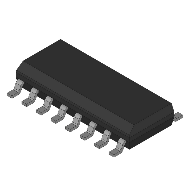
ICGOO电子元器件商城为您提供74HC139D,653由NXP Semiconductors设计生产,在icgoo商城现货销售,并且可以通过原厂、代理商等渠道进行代购。 74HC139D,653价格参考¥0.59-¥0.78。NXP Semiconductors74HC139D,653封装/规格:逻辑 - 信号开关,多路复用器,解码器, Decoder/Demultiplexer 1 x 2:4 16-SO。您可以下载74HC139D,653参考资料、Datasheet数据手册功能说明书,资料中有74HC139D,653 详细功能的应用电路图电压和使用方法及教程。
Nexperia USA Inc. 的74HC139D,653是一款高速CMOS逻辑器件,属于双2-4线译码器/解码器,广泛应用于数字电路系统中。该器件可将两个输入地址信号译码为四个互斥的低电平有效输出,常用于存储器地址解码、I/O端口选择和系统总线控制等场景。

典型应用场景包括微控制器系统中用于外设芯片(如RAM、ROM、UART等)的片选信号生成,实现多设备间的地址空间分配;在工业控制和通信设备中,作为逻辑控制单元的一部分,用于信号路由与模块切换;还可用于FPGA或CPLD外围电路中,简化地址译码逻辑,提高系统集成度。

74HC139D,653采用SO-14封装,工作电压范围为2V至6V,兼容TTL电平,具备低功耗、高抗干扰性和稳定可靠的特点,适用于消费电子、工业自动化、汽车电子和通信基础设施等领域。其引脚布局清晰,易于设计导入,是中小规模数字系统中常用的解码解决方案之一。
| 参数 | 数值 |
| 产品目录 | 集成电路 (IC)半导体 |
| 描述 | IC DECODER/DEMUX DUAL 16SOIC编码器、解码器、复用器和解复用器 DUAL 2-4 LINE DECODER/DEMUX |
| 产品分类 | |
| 品牌 | NXP Semiconductors |
| 产品手册 | |
| 产品图片 |
|
| rohs | 符合RoHS无铅 / 符合限制有害物质指令(RoHS)规范要求 |
| 产品系列 | 逻辑集成电路,编码器、解码器、复用器和解复用器,NXP Semiconductors 74HC139D,65374HC |
| 数据手册 | |
| 产品型号 | 74HC139D,653 |
| PCN封装 | |
| PCN组件/产地 | |
| 产品培训模块 | http://www.digikey.cn/PTM/IndividualPTM.page?site=cn&lang=zhs&ptm=24983 |
| 产品种类 | 编码器、解码器、复用器和解复用器 |
| 传播延迟时间 | 50 ns |
| 供应商器件封装 | 16-SO |
| 其它名称 | 568-7626-1 |
| 包装 | 剪切带 (CT) |
| 商标 | NXP Semiconductors |
| 安装类型 | 表面贴装 |
| 安装风格 | SMD/SMT |
| 封装 | Reel |
| 封装/外壳 | 16-SOIC(0.154",3.90mm 宽) |
| 封装/箱体 | SOT-109 |
| 工作温度 | -40°C ~ 125°C |
| 工厂包装数量 | 2500 |
| 最大工作温度 | + 125 C |
| 最小工作温度 | - 40 C |
| 标准包装 | 1 |
| 独立电路 | 2 |
| 电压-电源 | 2 V ~ 6 V |
| 电压源 | 单电源 |
| 电流-输出高,低 | 5.2mA,5.2mA |
| 电源电压-最大 | 6 V |
| 电源电压-最小 | 2 V |
| 电路 | 1 x 2:4 |
| 类型 | 解码器/多路分解器 |
| 输入/输出线数量 | 2 / 4 |
| 输入线路数量 | 2 |
| 输出线路数量 | 4 |
| 逻辑系列 | HC |
| 零件号别名 | 74HC139D-T |


- 商务部:美国ITC正式对集成电路等产品启动337调查
- 曝三星4nm工艺存在良率问题 高通将骁龙8 Gen1或转产台积电
- 太阳诱电将投资9.5亿元在常州建新厂生产MLCC 预计2023年完工
- 英特尔发布欧洲新工厂建设计划 深化IDM 2.0 战略
- 台积电先进制程称霸业界 有大客户加持明年业绩稳了
- 达到5530亿美元!SIA预计今年全球半导体销售额将创下新高
- 英特尔拟将自动驾驶子公司Mobileye上市 估值或超500亿美元
- 三星加码芯片和SET,合并消费电子和移动部门,撤换高东真等 CEO
- 三星电子宣布重大人事变动 还合并消费电子和移动部门
- 海关总署:前11个月进口集成电路产品价值2.52万亿元 增长14.8%


PDF Datasheet 数据手册内容提取
INTEGRATED CIRCUITS DATA SHEET For a complete data sheet, please also download: •The IC06 74HC/HCT/HCU/HCMOS Logic Family Specifications •The IC06 74HC/HCT/HCU/HCMOS Logic Package Information •The IC06 74HC/HCT/HCU/HCMOS Logic Package Outlines 74HC/HCT139 Dual 2-to-4 line decoder/demultiplexer Product specification September 1993 File under Integrated Circuits, IC06
Philips Semiconductors Product specification Dual 2-to-4 line decoder/demultiplexer 74HC/HCT139 FEATURES GENERAL DESCRIPTION • Demultiplexing capability The 74HC/HCT139 are high-speed Si-gate CMOS devices and are pin compatible with low power Schottky TTL • Two independent 2-to-4 decoders (LSTTL). It is specified in compliance with JEDEC • Multifunction capability standard no. 7A. • Active LOW mutually exclusive outputs The 74HC/HCT139 are high-speed, dual 2-to-4 line decoder/multiplexers. This device has two independent • Output capability: standard decoders, each accepting two binary weighted inputs • I category: MSI (nA and nA ) and providing four mutually exclusive active CC 0 1 LOW outputs (nY to nY3). Each decoder has an active 0 LOW enable input (nE). When nEis HIGH, every output is forced HIGH. The enable can be used as the data input for a 1-to-4 demultiplexer application. The “139” is identical to the HEF4556 of the HE4000B family. QUICK REFERENCE DATA GND = 0 V; T = 25(cid:176) C; t = t = 6 ns amb r f TYPICAL SYMBOL PARAMETER CONDITIONS UNIT HC HCT t / t propagation delay C = 15 pF; V = 5 V PHL PLH L CC nA to nY 11 13 ns n n nE to nY 10 13 ns 3 n C input capacitance 3.5 3.5 pF I C power dissipation capacitance per multiplexer notes 1 and 2 42 44 pF PD Notes 1. C is used to determine the dynamic power dissipation (P inm W): PD D P = C · V 2· f +(cid:229) (C · V 2· f )where: D PD CC i L CC o f = input frequency in MHz i f = output frequency in MHz o (cid:229) (C · V 2· f )= sum of outputs L CC o C =output load capacitance in pF L V =supply voltage in V CC 2. For HC the condition is V =GND to V I CC For HCT the condition is V =GND to V - 1.5 V I CC APPLICATIONS • Memory decoding or data-routing • Code conversion ORDERING INFORMATION See“74HC/HCT/HCU/HCMOS Logic Package Information”. September1993 2
Philips Semiconductors Product specification Dual 2-to-4 line decoder/demultiplexer 74HC/HCT139 PIN DESCRIPTION PIN NO. SYMBOL NAME AND FUNCTION 1, 15 1E, 2E enable inputs (active LOW) 2, 3 1A , 1A address inputs 0 1 4, 5, 6, 7 1Y to 1Y outputs (active LOW) 0 3 8 GND ground (0 V) 12, 11, 10, 9 2Y to 2Y outputs (active LOW) 0 3 14, 13 2A , 2A address inputs 0 1 16 V positive supply voltage CC Fig.1 Pin configuration. Fig.2 Logic symbol. (a) (b) Fig.3 IEC logic symbol. September1993 3
Philips Semiconductors Product specification Dual 2-to-4 line decoder/demultiplexer 74HC/HCT139 Fig.4 Functional diagram. FUNCTION TABLE INPUTS OUTPUTS nE nA nA nY nY nY nY 0 1 0 1 2 3 H X X H H H H L L L L H H H L H L H L H H L L H H H L H L H H H H H L Notes 1. H = HIGH voltage level L = LOW voltage level X = don’t care Fig.5 Logic diagram (one decoder/demultiplexer). September1993 4
Philips Semiconductors Product specification Dual 2-to-4 line decoder/demultiplexer 74HC/HCT139 DC CHARACTERISTICS FOR 74HC For the DC characteristics see“74HC/HCT/HCU/HCMOS Logic Family Specifications”. Output capability: standard I category: MSI CC AC CHARACTERISTICS FOR 74HC GND = 0 V; t = t = 6 ns; C = 50 pF r f L T ((cid:176) C) TEST CONDITIONS amb 74HC SYMBOL PARAMETER UNIT WAVEFORMS V +25 - 40to+85 - 40to+125 CC (V) min. typ. max. min. max. min. max. 39 145 180 220 2.0 propagation delay t / t 14 29 36 44 ns 4.5 Fig.6 PHL PLH nA toY n n 11 25 31 38 6.0 33 135 170 205 2.0 propagation delay t / t 12 27 34 41 ns 4.5 Fig.7 PHL PLH nEto nY n 10 23 29 35 6.0 19 75 95 110 2.0 output transition t / t 7 15 19 22 ns 4.5 Figs 6 and 7 THL TLH time 6 13 16 19 6.0 September1993 5
Philips Semiconductors Product specification Dual 2-to-4 line decoder/demultiplexer 74HC/HCT139 DC CHARACTERISTICS FOR HCT For the DC characteristics see“74HC/HCT/HCU/HCMOS Logic Family Specifications”. Output capability: standard I category: MSI CC Note to HCT types The value of additional quiescent supply current (D I ) for a unit load of 1 is given in the family specifications. CC To determineD I per input, multiply this value by the unit load coefficient shown in the table below. CC INPUT UNIT LOAD COEFFICIENT 1A 0.70 n 2A 0.70 n nE 1.35 AC CHARACTERISTICS FOR 74HCT GND = 0 V; t = t = 6 ns; C = 50 pF f f L T ((cid:176) C) TEST CONDITIONS amb 74HCT SYMBOL PARAMETER UNIT WAVEFORMS V +25 - 40to+85 - 40to+125 CC (V) min. typ. max. min. max. min. max. propagation delay t / t 16 34 43 51 ns 4.5 Fig.6 PHL PLH nA toY n n propagation delay t / t 16 34 43 51 ns 4.5 Fig.7 PHL PLH nEto nY n output transition t / t 7 15 19 22 ns 4.5 Figs 6 and 7 THL TLH time September1993 6
Philips Semiconductors Product specification Dual 2-to-4 line decoder/demultiplexer 74HC/HCT139 AC WAVEFORMS (1) HC : VM= 50%; VI= GND to VCC. HCT:VM= 1.3 V; VI=GND to 3 V. Fig.6 Waveforms showing the address input (nA )to output (nY ) propagation delays and the output transition n n times. (1) HC : VM= 50%; VI= GND to VCC. HCT:VM= 1.3 V; VI=GND to 3 V. Fig.7 Waveforms showing the enable input (nE) to output (nY )propagation delays and the output transition n times. PACKAGE OUTLINES See“74HC/HCT/HCU/HCMOS Logic Package Outlines”. September1993 7