ICGOO在线商城 > DKI06108

 Datasheet下载
- 型号: DKI06108
- 制造商: Sanken
- 库位|库存: xxxx|xxxx
- 要求:
| 数量阶梯 | 香港交货 | 国内含税 |
| +xxxx | $xxxx | ¥xxxx |
查看当月历史价格
查看今年历史价格
DKI06108产品简介:
ICGOO电子元器件商城为您提供DKI06108由Sanken设计生产,在icgoo商城现货销售,并且可以通过原厂、代理商等渠道进行代购。 提供DKI06108价格参考¥10.00-¥12.50以及SankenDKI06108封装/规格参数等产品信息。 你可以下载DKI06108参考资料、Datasheet数据手册功能说明书, 资料中有DKI06108详细功能的应用电路图电压和使用方法及教程。
| 参数 | 数值 |
| 产品目录 | |
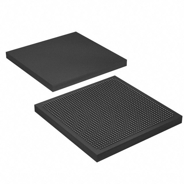
| 描述 | MOSFET N-CH 60V 47A TO-252 |
| 产品分类 | FET - 单 |
| FET功能 | 逻辑电平栅极,4.5V 驱动 |
| FET类型 | MOSFET N 通道,金属氧化物 |
| 品牌 | Sanken |
| 数据手册 | |
| 产品图片 |
|
| 产品型号 | DKI06108 |
| rohs | 无铅 / 符合限制有害物质指令(RoHS)规范要求 |
| 产品系列 | - |
| 不同Id时的Vgs(th)(最大值) | 2.5V @ 650µA |
| 不同Vds时的输入电容(Ciss) | 2520pF @ 25V |
| 不同Vgs时的栅极电荷(Qg) | 38.6nC @ 10V |
| 不同 Id、Vgs时的 RdsOn(最大值) | 9.1 mOhm @ 23.6A, 10V |
| 供应商器件封装 | TO-252-3 |
| 其它名称 | DKI06108DKR |
| 功率-最大值 | 47W |
| 包装 | Digi-Reel® |
| 安装类型 | 表面贴装 |
| 封装/外壳 | TO-252-3,DPak(2 引线+接片),SC-63 |
| 标准包装 | 1 |
| 漏源极电压(Vdss) | 60V |
| 电流-连续漏极(Id)(25°C时) | 47A (Tc) |


- 商务部:美国ITC正式对集成电路等产品启动337调查
- 曝三星4nm工艺存在良率问题 高通将骁龙8 Gen1或转产台积电
- 太阳诱电将投资9.5亿元在常州建新厂生产MLCC 预计2023年完工
- 英特尔发布欧洲新工厂建设计划 深化IDM 2.0 战略
- 台积电先进制程称霸业界 有大客户加持明年业绩稳了
- 达到5530亿美元!SIA预计今年全球半导体销售额将创下新高
- 英特尔拟将自动驾驶子公司Mobileye上市 估值或超500亿美元
- 三星加码芯片和SET,合并消费电子和移动部门,撤换高东真等 CEO
- 三星电子宣布重大人事变动 还合并消费电子和移动部门
- 海关总署:前11个月进口集成电路产品价值2.52万亿元 增长14.8%


PDF Datasheet 数据手册内容提取
60 V, 47 A, 7.2 mΩ Low RDS(ON) N ch Trench Power MOSFET DKI06108 Features Package V --------------------------------- 60 V (I = 100 µA) TO-252 (BR)DSS D (4) I ---------------------------------------------------------- 47 A D D R ---------- 9.7 mΩ max. (V = 10 V, I = 23.6 A) DS(ON) GS D Q ------ 16.9 nC (V = 4.5 V, V = 30 V, I = 28.5 A) g GS DS D Low Total Gate Charge High Speed Switching Low On-Resistance (1) (2) (3) (3) (2) (1) Capable of 4.5 V Gate Drive G D S S D G Not to scale 100 % UIL Tested RoHS Compliant Applications Equivalent circuit DC-DC converters Synchronous Rectification D(2)(4) Power Supplies G(1) S(3) Absolute Maximum Ratings Unless otherwise specified, T = 25 °C A Parameter Symbol Test conditions Rating Unit Drain to Source Voltage V 60 V DS Gate to Source Voltage V ± 20 V GS Continuous Drain Current I T = 25 °C 47 A D C PW ≤ 100µs Pulsed Drain Current I 94 A DM Duty cycle ≤ 1 % Continuous Source Current I 47 A (Body Diode) S Pulsed Source Current PW ≤ 100µs I 94 A (Body Diode) SM Duty cycle ≤ 1 % V = 30 V, L = 1 mH, DD I = 9.4 A, unclamped, Single Pulse Avalanche Energy E AS 89 mJ AS R = 4.7 Ω G Refer to Figure 1 Avalanche Current I 16.7 A AS Power Dissipation P T = 25 °C 47 W D C Operating Junction Temperature T 150 °C J Storage Temperature Range T − 55 to 150 °C STG DKI06108-DS Rev.1.5 SANKEN ELECTRIC CO.,LTD. 1 Mar. 11, 2015 http://www.sanken-ele.co.jp
DKI06108 Thermal Characteristics Unless otherwise specified, T = 25 °C A Parameter Symbol Test Conditions Min. Typ. Max. Unit Thermal Resistance R − − 2.7 °C/W (Junction to Case) θJC Thermal Resistance R Mounted on PCB* − − 35.7 °C/W (Junction to Ambient) θJA * 1 inch square 2 oz copper pad on 1.5 × 1.5 inch PCB. Electrical Characteristics Unless otherwise specified, T = 25 °C A Parameter Symbol Test Conditions Min. Typ. Max. Unit Drain to Source Breakdown V I = 100 μA, V = 0 V 60 − − V Voltage (BR)DSS D GS Drain to Source Leakage Current I V = 60 V, V = 0 V − − 100 µA DSS DS GS Gate to Source Leakage Current I V = ± 20 V − − ± 100 nA GSS GS Gate Threshold Voltage V V = V , I = 650 µA 1.0 2.0 2.5 V GS(th) DS GS D Static Drain to Source ID = 23.6 A, VGS = 10 V − 7.2 9.7 mΩ R On-Resistance DS(ON) I = 11.8 A, V = 4.5 V − 8.8 12.1 mΩ D GS Gate Resistance R f = 1 MHz − 1.5 − Ω G Input Capacitance C − 2520 − iss V = 25 V DS Output Capacitance C V = 0 V − 280 − pF oss GS f = 1 MHz Reverse Transfer Capacitance C − 135 − rss Total Gate Charge (V = 10 V) Q − 36.2 − GS g1 Total Gate Charge (V = 4.5 V) Q − 16.9 − GS g2 V = 30 V DS nC I = 28.5 A Gate to Source Charge Q D − 6.1 − gs Gate to Drain Charge Q − 5.4 − gd Turn-On Delay Time t − 4.5 − d(on) V = 30 V Rise Time t DD − 5.0 − r I = 28.5 A D ns V = 10 V, R = 4.7 Ω Turn-Off Delay Time t GS G − 21.6 − d(off) Refer to Figure 2 Fall Time t − 10.7 − f Source to Drain Diode Forward V I = 23.6 A, V = 0 V − 0.9 1.5 V Voltage SD S GS Source to Drain Diode Reverse Recovery Time trr IF = 28.5 A − 34.8 − ns di/dt = 100 A/µs Source to Drain Diode Reverse Q Refer to Figure 3 − 42.3 − nC Recovery Charge rr DKI06108-DS Rev.1.5 SANKEN ELECTRIC CO.,LTD. 2 Mar. 11, 2015
DKI06108 Test Circuits and Waveforms 1 V L E LI 2 (BR)DSS AS 2 AS V V (BR)DSS DD V(BR)DSS I D V DS I AS RG VDD V GS VDS VDD 0 V I D (a) Test Circuit (b) Waveform Figure 1 Unclamped Inductive Switching R L 90% V GS V 10% DS R V G VDD 90% GS V DS 0 V 10% t t t t P.W. = 10 μs d(on) r d(off) f Duty cycle ≤ 1 % t t on off (a) Test Circuit (b) Waveform Figure 2 Switching Time D.U.T. I L F I F VDD trr R G 0 V I × 90 % RM VGS di/dt 0 V I RM (a) Test Circuit (b) Waveform Figure 3 Diode Reverse Recovery Time DKI06108-DS Rev.1.5 SANKEN ELECTRIC CO.,LTD. 3 Mar. 11, 2015
DKI06108 RDS(ON)-ID characteristics (typical) RDS(ON)-ID characteristics (typical) ID-VGS characteristics (typical) VGS=10V VGS=4.5V VDS=5V 25 30 100 25 20 80 mΩ) 15 Tc = 125℃ mΩ)20 Tc = 125℃ 60 ON) ( 75℃ ON) (15 75℃ D (A) S( 10 S( I 40 Tc =125℃ RD 25℃ RD10 25℃ 75℃ 5 5 20 25℃ 0 0 0 0 20 40 60 80 100 0 20 40 60 80 100 0 1 2 3 4 5 6 VGS (V) ID (A) ID (A) IDR-VSDcharacteristics (typical) IDR-VSDcharacteristics (typical) VDS-VGS characteristics (typical) Tc=25℃ Tc=25℃ VDS=0V 0.3 100 100 VGS=10V 80 80 0.2 VDS (V) ID=18.9A IDR (A) 4600 VGS=4.35VV IDR (A) 4600 Tc =125℃ 0.1 ID=14.3A 75℃ ID=11.8A 20 0V 20 25℃ 0.0 0 0 0 5 10 15 0 0.5 1 1.5 0 0.5 1 1.5 VGS (V) VSD (V) VSD (V) Capacitance-VDS characteristics (typical) VGS -Qg characteristics(typical) Vth-Tc characteristics (typical) 10000 15 3 Ciss acitance (pF)1000 Coss VGS (V) 10 Vth (V) 2 p Ca 100 5 1 Crss ID=650uA Tc=25℃ VGS=VDS Ta=25℃ VDS=30V VGS=0V ID=28.5A 10 f=1MHz 0 0 0 10 20 30 40 50 0 10 20 30 40 25 50 75 100 125 150 Qg (nC) Tc (℃) VDS (V) RDS(ON)-Tc characteristics (typical) RDS(ON)-Tc characteristics (typical) BVDSS-Tc characteristics (typical) 20 20 78 76 16 16 74 ))N(mΩ12 ))N(mΩ 12 )DSS (V 72 (SO 8 (SO 8 BV 70 RD RD 68 ID=1mA 4 ID=23.6A 4 VGS=0V VGS=10V ID=11.8A 66 VGS=4.5V 0 0 64 25 50 75 100 125 150 25 50 75 100 125 150 25 50 75 100 125 150 Tc (℃) Tc (℃) Tc (℃) DKI06108-DS Rev.1.5 SANKEN ELECTRIC CO.,LTD. 4 Mar. 11, 2015
DKI06108 PD-Ta Derating SAFE OPERATING AREA 50 1000 ID(pulse)MAX 40 100 PT=100μs 30 W) D(A)10 PT=1ms ( 20 I D P 1 10 1 shot Tc=25℃ 0 0 50 100 150 0.10.1 1 10 100 VDS (V) Ta (℃) TRANSIENT THERMAL RESISTANCE -PULSE WIDTH 1.E+01 W) ℃/ 1.E+00 h j-c ( Rt 1.E-01 Tc = 25℃ 1shot VDS < 10V 1.E-02 1.E-04 1.E-03 1.E-02 1.E-01 1.E+00 1.E+01 1.E+02 P.T. (sec) DKI06108-DS Rev.1.5 SANKEN ELECTRIC CO.,LTD. 5 Mar. 11, 2015
DKI06108 Package Outline TO252 Symbol Min. Max. A 2.18 2.39 A1 -- 0.13 b 0.70 0.89 b1 0.70 0.86 b2 0.76 1.14 b3 4.95 5.46 c 0.46 0.61 c1 0.41 0.56 c2 0.46 0.89 D 5.97 6.22 D1 5.21 -- E 6.35 6.73 E1 4.32 -- e 2.29 H 9.40 10.41 L 1.40 1.78 L1 2.60 2.90 L2 0.51 L3 1.65 1.95 L4 0.60 0.90 L5 0.89 1.27 θ 1° 5° θ1 7°REF φ 1.20 REF NOTES: 1) Dimension is in millimeters 2) Pb-free. Device composition compliant with the RoHS directive Marking Diagram SK DKI××××× Part Number YMDD XXXB Lot Number Y is the Last digit of the year (0 to 9) M is the Month (1 to 9, O, N or D) DD is the Date (two digit of 01 to 31) XXX is the suffix No. B expresses Pb free pins DKI06108-DS Rev.1.5 SANKEN ELECTRIC CO.,LTD. 6 Mar. 11, 2015
DKI06108 OPERATING PRECAUTIONS In the case that you use Sanken products or design your products by using Sanken products, the reliability largely depends on the degree of derating to be made to the rated values. Derating may be interpreted as a case that an operation range is set by derating the load from each rated value or surge voltage or noise is considered for derating in order to assure or improve the reliability. In general, derating factors include electric stresses such as electric voltage, electric current, electric power etc., environmental stresses such as ambient temperature, humidity etc. and thermal stress caused due to self-heating of semiconductor products. For these stresses, instantaneous values, maximum values and minimum values must be taken into consideration. In addition, it should be noted that since power devices or IC’s including power devices have large self-heating value, the degree of derating of junction temperature affects the reliability significantly. Because reliability can be affected adversely by improper storage environments and handling methods, please observe the following cautions. Cautions for Storage Ensure that storage conditions comply with the standard temperature (5 to 35°C) and the standard relative humidity (around 40 to 75%); avoid storage locations that experience extreme changes in temperature or humidity. Avoid locations where dust or harmful gases are present and avoid direct sunlight. Reinspect for rust on leads and solderability of the products that have been stored for a long time. Cautions for Testing and Handling When tests are carried out during inspection testing and other standard test periods, protect the products from power surges from the testing device, shorts between the product pins, and wrong connections. Ensure all test parameters are within the ratings specified by Sanken for the products. Remarks About Using Thermal Silicone Grease When thermal silicone grease is used, it shall be applied evenly and thinly. If more silicone grease than required is applied, it may produce excess stress. The thermal silicone grease that has been stored for a long period of time may cause cracks of the greases, and it cause low radiation performance. In addition, the old grease may cause cracks in the resin mold when screwing the products to a heatsink. Fully consider preventing foreign materials from entering into the thermal silicone grease. When foreign material is immixed, radiation performance may be degraded or an insulation failure may occur due to a damaged insulating plate. The thermal silicone greases that are recommended for the resin molded semiconductor should be used. Our recommended thermal silicone grease is the following, and equivalent of these. Type Suppliers G746 Shin-Etsu Chemical Co., Ltd. YG6260 Momentive Performance Materials Japan LLC SC102 Dow Corning Toray Co., Ltd. Soldering When soldering the products, please be sure to minimize the working time, within the following limits: ・Reflow Preheat ; 180 °C / 90 ± 30 s Solder heating ; 250 °C / 10 ± 1s (260 °C peak, 2 times) ・Soldering iron ; 380 ± 10 °C / 3.5 ± 0.5s (1 time) Electrostatic Discharge When handling the products, the operator must be grounded. Grounded wrist straps worn should have at least 1MΩ of resistance from the operator to ground to prevent shock hazard, and it should be placed near the operator. Workbenches where the products are handled should be grounded and be provided with conductive table and floor mats. When using measuring equipment such as a curve tracer, the equipment should be grounded. When soldering the products, the head of soldering irons or the solder bath must be grounded in order to prevent leak voltages generated by them from being applied to the products. The products should always be stored and transported in Sanken shipping containers or conductive containers, or be wrapped in aluminum foil. DKI06108-DS Rev.1.5 SANKEN ELECTRIC CO.,LTD. 7 Mar. 11, 2015
DKI06108 IMPORTANT NOTES The contents in this document are subject to changes, for improvement and other purposes, without notice. Make sure that this is the latest revision of the document before use. Application examples, operation examples and recommended examples described in this document are quoted for the sole purpose of reference for the use of the products herein and Sanken can assume no responsibility for any infringement of industrial property rights, intellectual property rights, life, body, property or any other rights of Sanken or any third party which may result from its use. Unless otherwise agreed in writing by Sanken, Sanken makes no warranties of any kind, whether express or implied, as to the products, including product merchantability, and fitness for a particular purpose and special environment, and the information, including its accuracy, usefulness, and reliability, included in this document. Although Sanken undertakes to enhance the quality and reliability of its products, the occurrence of failure and defect of semiconductor products at a certain rate is inevitable. Users of Sanken products are requested to take, at their own risk, preventative measures including safety design of the equipment or systems against any possible injury, death, fires or damages to the society due to device failure or malfunction. Sanken products listed in this document are designed and intended for the use as components in general purpose electronic equipment or apparatus (home appliances, office equipment, telecommunication equipment, measuring equipment, etc.). When considering the use of Sanken products in the applications where higher reliability is required (transportation equipment and its control systems, traffic signal control systems or equipment, fire/crime alarm systems, various safety devices, etc.), and whenever long life expectancy is required even in general purpose electronic equipment or apparatus, please contact your nearest Sanken sales representative to discuss, prior to the use of the products herein. The use of Sanken products without the written consent of Sanken in the applications where extremely high reliability is required (aerospace equipment, nuclear power control systems, life support systems, etc.) is strictly prohibited. When using the products specified herein by either (i) combining other products or materials therewith or (ii) physically, chemically or otherwise processing or treating the products, please duly consider all possible risks that may result from all such uses in advance and proceed therewith at your own responsibility. Anti radioactive ray design is not considered for the products listed herein. Sanken assumes no responsibility for any troubles, such as dropping products caused during transportation out of Sanken’s distribution network. The contents in this document must not be transcribed or copied without Sanken’s written consent. DKI06108-DS Rev.1.5 SANKEN ELECTRIC CO.,LTD. 8 Mar. 11, 2015