ICGOO在线商城 > DC6M602X6/1215A,13

 Datasheet下载
- 型号: DC6M602X6/1215A,13
- 制造商: NXP Semiconductors
- 库位|库存: xxxx|xxxx
- 要求:
| 数量阶梯 | 香港交货 | 国内含税 |
| +xxxx | $xxxx | ¥xxxx |
查看当月历史价格
查看今年历史价格
DC6M602X6/1215A,13产品简介:
ICGOO电子元器件商城为您提供DC6M602X6/1215A,13由NXP Semiconductors设计生产,在icgoo商城现货销售,并且可以通过原厂、代理商等渠道进行代购。 提供DC6M602X6/1215A,13价格参考以及NXP SemiconductorsDC6M602X6/1215A,13封装/规格参数等产品信息。 你可以下载DC6M602X6/1215A,13参考资料、Datasheet数据手册功能说明书, 资料中有DC6M602X6/1215A,13详细功能的应用电路图电压和使用方法及教程。
DC6M602X6/1215A,13 是 NXP USA Inc.(现为恩智浦半导体)推出的一款高集成度 DC-DC 开关稳压器模块,属于 PMIC(电源管理集成电路)类别。该器件典型应用于对空间、效率与可靠性要求严苛的嵌入式与工业系统中。

主要应用场景包括:
• 工业自动化设备(如 PLC、传感器节点、IO 模块),为其微控制器(如 i.MX 系列)、FPGA 或通信接口(CAN、RS-485)提供稳定、低噪声的 3.3V/5V 或可配置输出电压;
• 汽车电子控制单元(ECU)中的次级电源轨,支持 AEC-Q100 认证的外围电路供电(需结合外围设计满足车规要求);
• 医疗便携设备(如手持诊断仪、监护模块),得益于其小尺寸封装(集成电感)、高转换效率(>90%)和低待机功耗,延长电池续航;
• 网络通信设备(如边缘网关、小型基站),为以太网 PHY、Wi-Fi/BLE 模组或 DDR 内存提供高效、低纹波的中间电源;
• 通用嵌入式系统(如基于 ARM Cortex-M/A 的开发平台),作为主电源后级的紧凑型 POL(Point-of-Load)稳压方案,简化电源设计并提升抗干扰能力。

该型号支持宽输入电压范围(通常为 4.5–18 V),具备过流、过热及短路保护,内置软启动与使能控制,适用于需要快速部署、高可靠性和低 EMI 的中低功率(典型输出电流 ≤2 A)场景。注意:具体参数应以官方最新数据手册(如 NXP DC6M602X6 系列文档)为准。
| 参数 | 数值 |
| 产品目录 | 集成电路 (IC) |
| 描述 | IC REG BUCK 1.2V/1.5V 6-WLCSP |
| 产品分类 | |
| 品牌 | NXP Semiconductors |
| 数据手册 | |
| 产品图片 |
|
| 产品型号 | DC6M602X6/1215A,13 |
| PCN过时产品 | |
| PWM类型 | - |
| rohs | 无铅 / 符合限制有害物质指令(RoHS)规范要求 |
| 产品系列 | - |
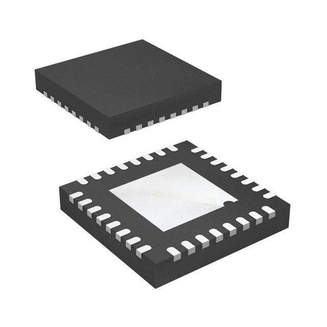
| 供应商器件封装 | 6-WLCSP(1.36x.96) |
| 其它名称 | 568-10423-6 |
| 包装 | Digi-Reel® |
| 同步整流器 | 是 |
| 安装类型 | 表面贴装 |
| 封装/外壳 | 6-XFBGA,WLCSP |
| 工作温度 | -40°C ~ 85°C |
| 标准包装 | 1 |
| 特色产品 | http://www.digikey.cn/product-highlights/zh/dc6m60xx6-family/50364 |
| 电压-输入 | 2.3 V ~ 5.5 V |
| 电压-输出 | 1.2V,1.5V |
| 电流-输出 | 650mA |
| 类型 | 降压(降压) |
| 输出数 | 1 |
| 输出类型 | 固定 |
| 频率-开关 | 6MHz |


- 商务部:美国ITC正式对集成电路等产品启动337调查
- 曝三星4nm工艺存在良率问题 高通将骁龙8 Gen1或转产台积电
- 太阳诱电将投资9.5亿元在常州建新厂生产MLCC 预计2023年完工
- 英特尔发布欧洲新工厂建设计划 深化IDM 2.0 战略
- 台积电先进制程称霸业界 有大客户加持明年业绩稳了
- 达到5530亿美元!SIA预计今年全球半导体销售额将创下新高
- 英特尔拟将自动驾驶子公司Mobileye上市 估值或超500亿美元
- 三星加码芯片和SET,合并消费电子和移动部门,撤换高东真等 CEO
- 三星电子宣布重大人事变动 还合并消费电子和移动部门
- 海关总署:前11个月进口集成电路产品价值2.52万亿元 增长14.8%


PDF Datasheet 数据手册内容提取
DC6M60xX6 family 6 MHz, 650 mA, ultra small DC-to-DC buck converter Rev. 2 — 29 January 2013 Product data sheet 1. Product profile 1.1 General description The DC6M60xX6 family consists of highly efficient 6MHz, 650mA step-down DC-to-DC converters. The devices convert input voltages between 2.3V and 5.5V to fixed output voltages of 1.2V, 1.5V, 1.8V or 2.85V. The devices of DC6M60xX6 family are optimized for battery-driven applications. Their high efficiency of up to 95% enables an extended battery life in all portable designs. Buck operation at a switching frequency of 6MHz allows using only a small low-cost 470nH coil and two capacitors. Besides working with standard chip inductors, the DC6M60xX6 family devices also support Printed-Circuit Board (PCB) coils and air coils. Product versions with and without automatic mode selection between Pulse Frequency Modulation(PFM) and Pulse Width Modulation (PWM) are available. Optionally the devices can be switched to forced PWM mode. 1.2 Features and benefits Efficiency up to95% Extremely low output ripple in PWM and PFM mode 2% total DC output voltage accuracy Soft start function for limiting inrush current Short circuit and over-temperature protection Integrated flyback diode Enable input operates with an active HIGH or with a clock signal Optional power good indicator output (XSHUTDOWN version) Wafer-Level Chip-Size Package (WLCSP) with 0.4 mm pitch 1.3 Applications Smartphones Tablet PCs Mobile handsets Mobile Internet Devices (MID) Digital Still Cameras (DSC) Portable Media Players (PMP) 1.4 Quick reference data I =650mA (max) Switching frequency f =6MHz O clk(PWM) V =1.2V, 1.5V, 1.8V or 2.85V V =2.3V to 5.5V O I Supply current I =0.2A in standby CC mode
DC6M60xX6 family NXP Semiconductors 6 MHz, 650 mA, ultra small DC-to-DC buck converter 2. Pinning information bump A1 index area MODE A1 A2 IN SW B1 B2 EN FB C1 C2 GND 018aaa210 Transparent top view solder balls facing down Fig 1. Pin configuration WLCSP6 T able 1. Pin description Symbol Pin Description MODE [1] A1 voltage select/mode select/XSHUTDOWN IN A2 supply input voltage SW B1 output voltage switch regulator EN B2 enable FB C1 control feedback GND C2 ground [1] Mode function depends on the chosen version of the buck converter as listed in Table3. DC6M60XX6_FAM All information provided in this document is subject to legal disclaimers. © NXP B.V. 2013. All rights reserved. Product data sheet Rev. 2 — 29 January 2013 2 of 26
DC6M60xX6 family NXP Semiconductors 6 MHz, 650 mA, ultra small DC-to-DC buck converter 3. Ordering information DC6M60xX6 family is available with different modes or output voltages and can be supplied upon request and acceptance from NXP Semiconductors. For more details, see Section19. Table 2. Ordering info rmation Type number Package Name Description Version DC6M60xX6 family WLCSP6 wafer-level chip-size package; 6 bumps (32) [1] - [1] Size 1.360.960.47mm 3.1 Ordering options Table 3. Ordering opt ions for DC6M601X6 and DC6M603X6[1] Type number Mode option Nominal output voltage (V ) O(nom) DC6M601X6/12S select automatic PWM/PFM or forcedPWMmode 1.2V DC6M601X6/15S select automatic PWM/PFM or forcedPWMmode 1.5V DC6M601X6/18S select automatic PWM/PFM or forcedPWMmode 1.8V DC6M601X6/285S select automatic PWM/PFM or forcedPWMmode 2.85V DC6M603X6/12A power good (XSHUTDOWN) output; automatic PWM/PFM mode 1.2V DC6M603X6/15A power good (XSHUTDOWN) output; automatic PWM/PFM mode 1.5V DC6M603X6/18A power good (XSHUTDOWN) output; automatic PWM/PFM mode 1.8V [1] For detail information about options see Section5, about functional selection see Section5.6. Table 4. Ordering opt ions for DC6M602X6[1] Type number Mode option Nominal output voltage (V ) O(nom) MODE = LOW MODE = HIGH DC6M602X6/1215A output voltage select; automatic PWM/PFM mode 1.2V 1.5V DC6M602X6/1218A output voltage select; automatic PWM/PFM mode 1.2V 1.8V DC6M602X6/1518A output voltage select; automatic PWM/PFM mode 1.5V 1.8V DC6M602X6/1215F output voltage select; forced PWM mode 1.2V 1.5V DC6M602X6/1218F output voltage select; forced PWM mode 1.2V 1.8V DC6M602X6/1518F output voltage select; forced PWM mode 1.5V 1.8V [1] For detail information about options see Section5, about functional selection see Section5.6. DC6M60XX6_FAM All information provided in this document is subject to legal disclaimers. © NXP B.V. 2013. All rights reserved. Product data sheet Rev. 2 — 29 January 2013 3 of 26
DC6M60xX6 family NXP Semiconductors 6 MHz, 650 mA, ultra small DC-to-DC buck converter 3.1.1 Naming convention (cid:2)(cid:3)(cid:4)(cid:5)(cid:4)(cid:6)(cid:7)(cid:8)(cid:4)(cid:9)(cid:10)(cid:11)(cid:10)(cid:12)(cid:13) (cid:14)(cid:15)(cid:16)(cid:17)(cid:18)(cid:16)(cid:19)(cid:20)(cid:21) (cid:5)"#(cid:18)*%(cid:27)$"(cid:19)(cid:22)"(cid:28)(cid:27)$"(cid:19) (cid:4)(cid:5)(cid:22)(cid:23)(cid:22)(cid:4)(cid:22)(cid:5)(cid:24)(cid:25) (cid:13)(cid:22)(cid:23)(cid:22)%(cid:18)(cid:27)"(cid:22)!"#(cid:18)*%(cid:27)$"(cid:19)(cid:22)(cid:29)&(cid:14)(cid:5)(cid:22)"(cid:15)(cid:22)&’(cid:5)(cid:31) (cid:14)(cid:22)(cid:23)(cid:22)("(cid:15)(cid:20)(cid:16)#(cid:22)&’(cid:5)(cid:22)!"#(cid:16) /(cid:22)(cid:23)(cid:22))(cid:16)*(cid:16)(cid:20)(cid:27)(cid:22)!"#(cid:18)*%(cid:27)$"(cid:19) (cid:26)(cid:18)(cid:27)(cid:28)(cid:18)(cid:27)(cid:22)(cid:20)(cid:18)(cid:15)(cid:15)(cid:16)(cid:19)(cid:27)(cid:22)(cid:29)(cid:30)(cid:26)(cid:31) (cid:22)(cid:23)(cid:22) (cid:7)(cid:11)(cid:22)!(cid:13) (cid:26)(cid:18)(cid:27)(cid:28)(cid:18)(cid:27)(cid:22)+"*(cid:27)%,(cid:16)(cid:22)(cid:29)5(cid:26)(cid:31) (cid:11)(cid:22)(cid:23)(cid:22)(cid:11)(cid:6)(cid:6)(cid:22)!(cid:13) (cid:10)(cid:7)(cid:22)(cid:23)(cid:22)(cid:10)6(cid:7)(cid:22)5 (cid:4)(cid:22)(cid:23)(cid:22)(cid:4)(cid:11)(cid:6)(cid:22)!(cid:13) &%(cid:20)3%,(cid:16)(cid:22)$#(cid:16)(cid:19)(cid:27)$($(cid:16)(cid:15) (cid:10)(cid:11)(cid:22)(cid:23)(cid:22)(cid:10)6(cid:11)(cid:22)5 (cid:8)(cid:4)(cid:22)(cid:23)(cid:22)’4(cid:3)/&(cid:4) (cid:10)(cid:11)(cid:10)(cid:12)(cid:22)(cid:23)(cid:22)(cid:10)6(cid:11)(cid:22)5(cid:22)"(cid:15)(cid:22)(cid:10)6(cid:12)(cid:22)5 (cid:5)"#(cid:16)(cid:22)"(cid:28)(cid:27)$"(cid:19) (cid:10)(cid:22)(cid:23)(cid:22)%(cid:18)(cid:27)"(cid:22)&’(cid:5)(cid:9)&(cid:14)(cid:5)(cid:22)"(cid:15)(cid:22)("(cid:15)(cid:20)(cid:16)#(cid:22)&’(cid:5)(cid:22))(cid:16)*(cid:16)(cid:20)(cid:27) (cid:7)(cid:22)(cid:23)(cid:22)+"*(cid:27)%,(cid:16)(cid:22))(cid:16)*(cid:16)(cid:20)(cid:27) -(cid:22)(cid:23)(cid:22)(cid:28)".(cid:16)(cid:15)(cid:22),""#(cid:22)(cid:29)(cid:8)/(cid:24)01(cid:2)(cid:26)’2(cid:31)(cid:22)"(cid:18)(cid:27)(cid:28)(cid:18)(cid:27) (cid:2)(cid:2)(cid:2)(cid:3)(cid:4)(cid:4)(cid:5)(cid:4)(cid:6)(cid:7) Fig 2. Naming convention 4. Block diagram (cid:4)(cid:3) (cid:7)(cid:8)(cid:9)(cid:4) (cid:2)(cid:3) (cid:2)(cid:3) (cid:6)(cid:17)(cid:3)(cid:9)(cid:12)(cid:17)(cid:18) (cid:13)(cid:14)(cid:15)(cid:16) (cid:19)(cid:4)(cid:7)(cid:18)(cid:4)(cid:20)(cid:17)(cid:19)(cid:21)(cid:20)(cid:4) (cid:11)(cid:17)(cid:19)(cid:22)(cid:23)(cid:9)(cid:8)(cid:12) (cid:5)(cid:6) (cid:7)(cid:8)(cid:9)(cid:4) (cid:8)(cid:13)(cid:4)(cid:20)(cid:22)(cid:21)(cid:20)(cid:20)(cid:4)(cid:3)(cid:19) (cid:22)(cid:8)(cid:3)(cid:19)(cid:20)(cid:8)(cid:25) (cid:9)(cid:4)(cid:19)(cid:4)(cid:22)(cid:19)(cid:8)(cid:20) (cid:6)(cid:2)(cid:17)(cid:10)(cid:24)(cid:10)(cid:21)(cid:18)(cid:18)(cid:25)(cid:26) (cid:20)(cid:28) (cid:18)(cid:11)(cid:7)(cid:24)(cid:12)(cid:4)(cid:3)(cid:4)(cid:20)(cid:17)(cid:19)(cid:8)(cid:20) (cid:17)(cid:3)(cid:9) (cid:12)(cid:17)(cid:19)(cid:4)(cid:24)(cid:9)(cid:20)(cid:2)(cid:13)(cid:4)(cid:20) (cid:10)(cid:11) (cid:18)(cid:8)(cid:11)(cid:4)(cid:20)(cid:24)(cid:10)(cid:17)(cid:13)(cid:4)(cid:24)(cid:7)(cid:8)(cid:9)(cid:4) (cid:13)(cid:14)(cid:15)(cid:16) (cid:25)(cid:8)(cid:12)(cid:2)(cid:22) (cid:20)(cid:29) (cid:27)(cid:4)(cid:20)(cid:8)(cid:24)(cid:22)(cid:21)(cid:20)(cid:20)(cid:4)(cid:3)(cid:19) (cid:10)(cid:8)(cid:5)(cid:19)(cid:24)(cid:10)(cid:19)(cid:17)(cid:20)(cid:19) (cid:9)(cid:4)(cid:19)(cid:4)(cid:22)(cid:19)(cid:8)(cid:20) (cid:12)(cid:3)(cid:9) (cid:2)(cid:2)(cid:2)(cid:3)(cid:4)(cid:4)(cid:5)(cid:4)(cid:5)(cid:4) Fig 3. Block diagram DC6M60XX6_FAM All information provided in this document is subject to legal disclaimers. © NXP B.V. 2013. All rights reserved. Product data sheet Rev. 2 — 29 January 2013 4 of 26
DC6M60xX6 family NXP Semiconductors 6 MHz, 650 mA, ultra small DC-to-DC buck converter 5. Functional description The step-down converter (Figure4) generates a regulated constant output voltage behind an externally connected coil at pin SW. For this operation only the inductor and two filter capacitors are required. No additional flyback diode is needed. Place the pick-off pin for FB behind the inductor to sense the output voltage. 5(cid:30) (cid:13)(cid:7) (cid:13)(cid:10) (cid:30)2 (cid:5)(cid:26)(cid:2)7 9(cid:7) 9(cid:10) 4"(cid:29)(cid:16):(cid:27)(cid:31) 5(cid:26) 72 /’ (cid:3)$(cid:29)(cid:16):(cid:27)(cid:31) (cid:3)(cid:7) (cid:3)(cid:10) (cid:3)"(cid:29)(cid:16):(cid:27)(cid:31) 82(cid:2) (cid:14)9 (cid:2)(cid:2)(cid:2)(cid:3)(cid:4)(cid:4)(cid:5)(cid:4)(cid:5)(cid:8) Fig 4. Simple application schematic The step-down converter starts a switching cycle with an active P-channel MOS(PMOS) which allows rising the output voltage until a defined value is reached. Then the feedback circuit turns off the PMOS switch and turns on the N-channel MOS (NMOS) as active rectification. The step-down converter (Figure3) consists of an integrated oscillator. It runs at high frequency to compare the return path and to control the PWM/PFM logic block and the break-before-make circuit of the integrated NMOS and PMOS transistor. This allows reaching constant output voltage with high efficiency and low output ripple. 5.1 Automatic PWM/PFM mode Battery-driven applications need power-saving options. Therefore the DC-to-DC converter provides a current-sensing circuit which detects the output current. Ifthe current is below a certain threshold, the system switches to PFM mode. In this operation, the converter uses less current and saves battery operation time. This automode can be switched off to the forced PFM mode (see Section5.6). 5.2 Inrush current limiter (soft start) The DC6M60xX6 family has an integrated soft start function to limit the maximum inrush current and to reduce an input voltage dip. Therefore the system has a turn-on procedure which starts up step-by-step over 300s and limits the inrush current via a duty cycle control up to the maximum current capability. 5.3 Thermal protection The DC6M60xX6 family products have an integrated thermal protection. The protection circuit senses the internal temperature of the chip and switches off the integrated PMOS power switch transistor when a defined maximum temperature is reached. After the temperature returns to a safe value, the system restarts with a soft start. DC6M60XX6_FAM All information provided in this document is subject to legal disclaimers. © NXP B.V. 2013. All rights reserved. Product data sheet Rev. 2 — 29 January 2013 5 of 26
DC6M60xX6 family NXP Semiconductors 6 MHz, 650 mA, ultra small DC-to-DC buck converter 5.4 Short-circuit and overcurrent protection The short-circuit and overcurrent protection senses the current through the integrated PMOS high-side driver. If the diagnostic circuit detects an overcurrent, the system switches off the PMOS to break the current flow. 5.5 Enable (EN) All products have an enable pin EN which enables the device by a constant logic HIGH signal but also by applying an alternating (clock) signal to the enable pin. All devices start with a soft start (Section5.2). If EN is forced to a LOW level, the system is in Power-down mode. Then the input current is negligible and the output voltage sets to LOW via a resistor. It is possible to enable all DC6M60xX6 family products by applying a clock signal which is used to enable other parts of a certain circuit such as camera modules based on the Standard Mobile Imaging Architecture (SMIA) specification. The required signal frequency has to be in the range of 5MHz to 27MHz with a duty cycle between 40% and 60%. Table 5. Function selection EN logic level Description HIGH or clock signal operation LOW shut down 5.6 Function selection (MODE) Depending on the product version, three different operation modes are available for the MODE pin. 5.6.1 Automatic PWM/PFM and forced PWM mode The default operation mode is the automatic selection mode. This mode switches the device between PWM and PFM to reduce power consumption as described in Section5.1. The automatic mode of DC6M601X6 can be switched off to use only the PWM mode. DC6M602X6 does not have this option but is available with fix mode (automatic or forced PWM). Table 6. Function selection DC6M601X6 MODE logic level Description LOW automatic PWM/PFM mode HIGH forced PWM mode 5.6.2 Output voltage select DC6M602X6 offers the option to select the output voltage V depending on the logic level O applied to the MODE pin. Depending on the logic input level either the LOW or the HIGH output voltage is selected. Table7 illustrates this behavior. DC6M60XX6_FAM All information provided in this document is subject to legal disclaimers. © NXP B.V. 2013. All rights reserved. Product data sheet Rev. 2 — 29 January 2013 6 of 26
DC6M60xX6 family NXP Semiconductors 6 MHz, 650 mA, ultra small DC-to-DC buck converter Table 7. Output voltage selection DC6M602X6 MODE logic level Output voltage LOW low voltage HIGH high voltage The MODE input pin has no default level. To prevent undefined states, it has to be applied with a clear LOW or HIGH level. 5.6.3 Power good output (XSHUTDOWN) DC6M603X6 has an XSHUTDOWN or power good output. This function is often used when the converter is turned on by a clock signal (CLK) available at pin MODE. The basic timing is depicted in Figure5 and Table8 where EXTCLK is the clock signal at the enable input and V the DC-to-DC converter output voltage. The XSHUTDOWN is the O power good signal and has the same signal output level as V . O 7(cid:8)1(cid:3)4; (cid:29)72(cid:31) 1(cid:10) 1 5(cid:26) 1(cid:11) (cid:8)/(cid:24)01(cid:2)(cid:26)’2 (cid:29)(cid:5)(cid:26)(cid:2)7(cid:31) 1(cid:7) 1- (cid:2)(cid:2)(cid:2)(cid:3)(cid:4)(cid:4)(cid:5)(cid:4)(cid:5)(cid:9) Fig 5. Timing XSHUTDOWN enable/disable T able 8. Timing XSHUTDOWN Symbol Description Min Max Unit T1 EXTCLK active - V rising 10 100 s O T2 V settled - XSHUTDOWN rising 0 100 s O T3 V down time; C = 10pF; load current I = 20mA 0 1000 s O o(ext) L T4 EXTCLK inactive - XSHUTDOWN down 0 100 s T5 V rising time (no-load) 30 200 s O DC6M60XX6_FAM All information provided in this document is subject to legal disclaimers. © NXP B.V. 2013. All rights reserved. Product data sheet Rev. 2 — 29 January 2013 7 of 26
DC6M60xX6 family NXP Semiconductors 6 MHz, 650 mA, ultra small DC-to-DC buck converter 6. Limiting values Table 9. Limiting values In accordance with the Absolute Maximum Rating System (IEC 60134). Symbol Parameter Conditions Min Max Unit V voltage on pin IN 4ms transient 0.5 +6.0 V IN V input voltage on pins EN, MODE, FB 0.5 +5.5 V I V output voltage on pin SW 0.5 +5.5 V O P total power dissipation - 800 mW tot T storage temperature 55 +150 C stg T junction temperature 30 +125 C j T ambient temperature 40 +85 C amb V electrostatic discharge human body model 2 +2 kV ESD voltage (JESD22-001) machine model 200 +200 V (JESD22-A115) 7. Recommended operating conditions Table 10. Operating conditions At recommended operating conditions; T =25C; voltages are referenced to GND (0V); unless amb otherwise specified. Symbol Parameter Conditions Min Typ Max Unit V voltage on pin IN 2.3 - 5.5 V IN V input voltage on pins EN, MODE, FB -0.5 - V + V I IN 0.3 I output current 0 - 650 mA O C external input [1] - 4.7 10 F i(ext) capacitance C external output [1] 2.2 4.7 - F o(ext) capacitance L external output [1] - 0.47 - H o(ext) inductance [1] See Section 10 “Application information”. DC6M60XX6_FAM All information provided in this document is subject to legal disclaimers. © NXP B.V. 2013. All rights reserved. Product data sheet Rev. 2 — 29 January 2013 8 of 26
DC6M60xX6 family NXP Semiconductors 6 MHz, 650 mA, ultra small DC-to-DC buck converter 8. Static characteristics Table 11. Characterist ics At recommended input voltages and T = 40C to +85C; voltages are referenced to GND (ground = 0 V); unless amb otherwise specified. Symbol Parameter Conditions Min Typ Max Unit Input voltage and input current V input voltage V = 1.2V 2.3 - 5.5 V I O V = 1.5V 2.3 - 5.5 V O V = 1.8V 2.8 - 5.5 V O V = 2.85V 3.7 - 5.5 V O I supply current operating; PWMmode; - 8 - mA CC I =0A O operating; PFMmode; - 180 - A I =0A O disabled - 0.2 - A Output voltage and output current V output voltage I 15mA [1] 0.98 V 1.02 V O O O(nom) V V O(nom) O(nom) 0 mA < I < 15 mA; [1] 0.98 V 1.04 V O O(nom) autoPWM/PFM mode V V O(nom) O(nom) I maximum output current 650 - - mA O(max) V peak-to-peak ripple output voltage 0mA<I <100mA; [1] - - 10 mV o(ripple)(p-p) O V =V +1.2V I O(nom) 100mA<I <650mA; [1] - 7 15 mV O V =V +1.2V I O(nom) Line regulation V /V output voltage variation as a 2.3V<V <5.5V; - 0.03 - %/V O I I function of input voltage variation I=200mA Load regulation V /I output voltage variation as a 0 A<I <650mA - 0.003 - %/mA O L O function of load current variation Pin EN V HIGH-level input voltage 1 - - V IH V LOW-level input voltage - - 0.4 V IL I HIGH-level input current V =1.2V - - 1 A IH IH Pin MODE V HIGH-level input voltage 1 - - V IH V LOW-level input voltage - - 0.4 V IL I HIGH-level input current V =1.2V - - 1 A IH IH V HIGH-level output voltage [2] 0.9 V - 1.1 V V OH O O V LOW-level output voltage [2] 0.1 - 0.3 V OL Clock frequency and duty cycle f PWM clock frequency 5.4 6.0 6.6 MHz clk(PWM) f PFM clock frequency 0 - 6.6 MHz clk(PFM) DC6M60XX6_FAM All information provided in this document is subject to legal disclaimers. © NXP B.V. 2013. All rights reserved. Product data sheet Rev. 2 — 29 January 2013 9 of 26
DC6M60xX6 family NXP Semiconductors 6 MHz, 650 mA, ultra small DC-to-DC buck converter Table 11. Characteristics …continued At recommended input voltages and T = 40C to +85C; voltages are referenced to GND (ground = 0 V); unless amb otherwise specified. Symbol Parameter Conditions Min Typ Max Unit duty cycle forced PWM mode DC6M601X6/285S 2 - 100 % all other devices 2 - 92 % automatic forced PWM / PFM mode DC6M601X6/285S 0 - 100 % all other devices 0 - 92 % Overtemperature and overcurrent protection T shutdown temperature - 150 - C sd T shutdown temperature hysteresis - 40 - K sd(hys) I output current limit 1.0 1.3 - A Olim I inrush current limit - 0.3 - A inrush(lim) Switches R drain-source on-state resistance P-channel FET; V =3.6V - 0.15 - DSon DS N-channel FET; V =3.6V - 0.3 - DS I leakage current V = 5V - - 1 A leak DS [1] V = nominal output voltage (device specific). O(nom) [2] Only for product versions with power good output (DC6M603X6). 9. Dynamic characteristics 9.1 Efficiency (cid:2)(cid:2)(cid:2)(cid:3)(cid:4)(cid:4)(cid:10)(cid:5)(cid:6)(cid:11) (cid:2)(cid:2)(cid:2)(cid:3)(cid:4)(cid:4)(cid:5)(cid:4)(cid:5)(cid:12) (cid:10)(cid:6)(cid:6) (cid:10)(cid:6)(cid:6) (cid:16)(cid:16)(cid:16)(((((($$$(cid:20)(cid:20)(cid:20)$$$(cid:16)(cid:16)(cid:16)(cid:19)(cid:19)(cid:19)(cid:20)(cid:20)(cid:20)(cid:21)(cid:21)(cid:21) (cid:16)(cid:16)(cid:16)(((((($$$(cid:20)(cid:20)(cid:20)$$$(cid:16)(cid:16)(cid:16)(cid:19)(cid:19)(cid:19)(cid:20)(cid:20)(cid:20)(cid:21)(cid:21)(cid:21) (cid:29)(cid:29)(cid:29)===(cid:31)(cid:31)(cid:31) (cid:29)(cid:29)(cid:29)===(cid:31)(cid:31)(cid:31) (cid:12)(cid:6) (cid:12)(cid:6) (cid:4)(cid:6) (cid:4)(cid:6) 55(cid:30)(cid:30)(cid:22)(cid:22)(cid:22)(cid:23)(cid:23)(cid:23)(cid:22)(cid:22)(cid:22)(cid:22)(cid:22)(cid:22)---666(cid:6)(cid:6)(cid:6)(cid:22)(cid:22)(cid:22)555 55(cid:30)(cid:30)(cid:22)(cid:22)(cid:22)(cid:23)(cid:23)(cid:23)(cid:22)(cid:22)(cid:22)(cid:22)(cid:22)(cid:22)(cid:7)(cid:7)(cid:7)666---(cid:22)(cid:22)(cid:22)555 55(cid:30)(cid:30)(cid:22)(cid:22)(cid:22)(cid:23)(cid:23)(cid:23)(cid:22)(cid:22)(cid:22)(cid:22)(cid:22)(cid:22)---666(cid:7)(cid:7)(cid:7)(cid:22)(cid:22)(cid:22)555 55(cid:30)(cid:30)(cid:22)(cid:22)(cid:22)(cid:23)(cid:23)(cid:23)(cid:22)(cid:22)(cid:22)(cid:22)(cid:22)(cid:22)(cid:7)(cid:7)(cid:7)666(cid:12)(cid:12)(cid:12)(cid:22)(cid:22)(cid:22)555 55(cid:30)(cid:30)(cid:22)(cid:22)(cid:22)(cid:23)(cid:23)(cid:23)(cid:22)(cid:22)(cid:22)(cid:22)(cid:22)(cid:22)---666(cid:4)(cid:4)(cid:4)(cid:22)(cid:22)(cid:22)555 55(cid:30)(cid:30)(cid:22)(cid:22)(cid:22)(cid:23)(cid:23)(cid:23)(cid:22)(cid:22)(cid:22)(cid:22)(cid:22)(cid:22)---666(cid:7)(cid:7)(cid:7)(cid:22)(cid:22)(cid:22)555 (cid:6) 55(cid:30)(cid:30)(cid:22)(cid:22)(cid:22)(cid:23)(cid:23)(cid:23)(cid:22)(cid:22)(cid:22)(cid:22)(cid:22)(cid:22) 666(cid:7)(cid:7)(cid:7)(cid:22)(cid:22)(cid:22)555 (cid:6) 55(cid:30)(cid:30)(cid:22)(cid:22)(cid:22)(cid:23)(cid:23)(cid:23)(cid:22)(cid:22)(cid:22)(cid:22)(cid:22)(cid:22)---666(cid:4)(cid:4)(cid:4)(cid:22)(cid:22)(cid:22)555 55(cid:30)(cid:30)(cid:22)(cid:22)(cid:22)(cid:23)(cid:23)(cid:23)(cid:22)(cid:22)(cid:22)(cid:22)(cid:22)(cid:22)(cid:11)(cid:11)(cid:11)666(cid:6)(cid:6)(cid:6)(cid:22)(cid:22)(cid:22)555 55(cid:30)(cid:30)(cid:22)(cid:22)(cid:22)(cid:23)(cid:23)(cid:23)(cid:22)(cid:22)(cid:22)(cid:22)(cid:22)(cid:22) 666(cid:7)(cid:7)(cid:7)(cid:22)(cid:22)(cid:22)555 (cid:7)(cid:6) (cid:7)(cid:6) (cid:6) (cid:6) (cid:6) (cid:10)(cid:6)(cid:6) (cid:7)(cid:6)(cid:6) -(cid:6)(cid:6) (cid:6)(cid:6) (cid:11)(cid:6)(cid:6) (cid:4)(cid:6)(cid:6) <(cid:6)(cid:6) (cid:6) (cid:10)(cid:6)(cid:6) (cid:7)(cid:6)(cid:6) -(cid:6)(cid:6) (cid:6)(cid:6) (cid:11)(cid:6)(cid:6) (cid:4)(cid:6)(cid:6) <(cid:6)(cid:6) (cid:30)(cid:26)(cid:22)(cid:29)!(cid:13)(cid:31) (cid:30)(cid:26)(cid:22)(cid:29)!(cid:13)(cid:31) V =2.85V V =1.8V O O Fig 6. DC6M60xX6/285x: Efficiency as a function of Fig 7. DC6M60xX6/18x: Efficiency as a function of output current output current DC6M60XX6_FAM All information provided in this document is subject to legal disclaimers. © NXP B.V. 2013. All rights reserved. Product data sheet Rev. 2 — 29 January 2013 10 of 26
DC6M60xX6 family NXP Semiconductors 6 MHz, 650 mA, ultra small DC-to-DC buck converter (cid:2)(cid:2)(cid:2)(cid:3)(cid:4)(cid:4)(cid:10)(cid:5)(cid:6)(cid:13) (cid:10)(cid:6)(cid:6) (cid:16)(cid:16)(cid:16)(((((($$$(cid:20)(cid:20)(cid:20)$$$(cid:16)(cid:16)(cid:16)(cid:19)(cid:19)(cid:19)(cid:20)(cid:20)(cid:20)(cid:21)(cid:21)(cid:21) (cid:29)(cid:29)(cid:29)===(cid:31)(cid:31)(cid:31) (cid:12)(cid:6) (cid:4)(cid:6) (cid:6) 55(cid:30)(cid:30)(cid:22)(cid:22)(cid:22)(cid:23)(cid:23)(cid:23)(cid:22)(cid:22)(cid:22)(cid:22)(cid:22)(cid:22)(cid:7)(cid:7)(cid:7)666---(cid:22)(cid:22)(cid:22)555 55(cid:30)(cid:30)(cid:22)(cid:22)(cid:22)(cid:23)(cid:23)(cid:23)(cid:22)(cid:22)(cid:22)(cid:22)(cid:22)(cid:22)(cid:7)(cid:7)(cid:7)666(cid:12)(cid:12)(cid:12)(cid:22)(cid:22)(cid:22)555 55(cid:30)(cid:30)(cid:22)(cid:22)(cid:22)(cid:23)(cid:23)(cid:23)(cid:22)(cid:22)(cid:22)(cid:22)(cid:22)(cid:22)---666(cid:7)(cid:7)(cid:7)(cid:22)(cid:22)(cid:22)555 (cid:7)(cid:6) 55(cid:30)(cid:30)(cid:22)(cid:22)(cid:22)(cid:23)(cid:23)(cid:23)(cid:22)(cid:22)(cid:22)(cid:22)(cid:22)(cid:22)---666(cid:4)(cid:4)(cid:4)(cid:22)(cid:22)(cid:22)555 55(cid:30)(cid:30)(cid:22)(cid:22)(cid:22)(cid:23)(cid:23)(cid:23)(cid:22)(cid:22)(cid:22)(cid:22)(cid:22)(cid:22) 666(cid:7)(cid:7)(cid:7)(cid:22)(cid:22)(cid:22)555 (cid:6) (cid:6) (cid:10)(cid:6)(cid:6) (cid:7)(cid:6)(cid:6) -(cid:6)(cid:6) (cid:6)(cid:6) (cid:11)(cid:6)(cid:6) (cid:4)(cid:6)(cid:6) <(cid:6)(cid:6) (cid:30)(cid:26)(cid:22)(cid:29)!(cid:13)(cid:31) V =1.2V O Fig 8. DC6M60xX6/12x: Efficiency as a function of output current 9.2 Output voltage ripple (cid:2)(cid:2)(cid:2)(cid:3)(cid:4)(cid:4)(cid:5)(cid:9)(cid:7)(cid:9) -(cid:6) 5"(cid:29)(cid:15)$(cid:28)(cid:28)*(cid:16)(cid:31)(cid:29)(cid:28)>(cid:28)(cid:31) (cid:29)(cid:29)!!55(cid:31)(cid:31) (cid:7)(cid:11) (cid:7)(cid:6) 5(cid:30)(cid:22)(cid:23)(cid:22)(cid:11)6(cid:11)(cid:22)5 (cid:10)(cid:11) 5(cid:30)(cid:22)(cid:23)(cid:22) 6(cid:7)(cid:22)5 5(cid:30)(cid:22)(cid:23)(cid:22)-6(cid:4)(cid:22)5 5(cid:30)(cid:22)(cid:23)(cid:22)-6(cid:6)(cid:22)5 (cid:10)(cid:6) (cid:11) (cid:6) (cid:6) (cid:10)(cid:6)(cid:6) (cid:7)(cid:6)(cid:6) -(cid:6)(cid:6) (cid:6)(cid:6) (cid:11)(cid:6)(cid:6) (cid:4)(cid:6)(cid:6) <(cid:6)(cid:6) (cid:30)(cid:26)(cid:22)(cid:29)!(cid:13)(cid:31) V =1.8V O Fig 9. DC6M60xX6/18x: Peak-to-peak output voltage ripple as a function of output current DC6M60XX6_FAM All information provided in this document is subject to legal disclaimers. © NXP B.V. 2013. All rights reserved. Product data sheet Rev. 2 — 29 January 2013 11 of 26
DC6M60xX6 family NXP Semiconductors 6 MHz, 650 mA, ultra small DC-to-DC buck converter 9.3 Output voltage variation (cid:2)(cid:2)(cid:2)(cid:3)(cid:4)(cid:4)(cid:10)(cid:5)(cid:6)(cid:7) (cid:10)6(cid:12)(cid:11) 55(cid:26)(cid:26) (cid:29)(cid:29)(cid:29)555(cid:31)(cid:31)(cid:31) (cid:10)6(cid:12)- 11%%%!!!???(cid:22)(cid:22)(cid:22)(cid:23)(cid:23)(cid:23)(cid:22)(cid:22)(cid:22)(cid:22)(cid:22)(cid:22)>>> (cid:6)(cid:6)(cid:6)(cid:22)(cid:22)(cid:22)@@@(cid:3)(cid:3)(cid:3) 11%%%!!!???(cid:22)(cid:22)(cid:22)(cid:23)(cid:23)(cid:23)(cid:22)(cid:22)(cid:22)(cid:22)(cid:22)(cid:22)(cid:12)(cid:12)(cid:12)(cid:11)(cid:11)(cid:11)(cid:22)(cid:22)(cid:22)@@@(cid:3)(cid:3)(cid:3) 11%%%!!!???(cid:22)(cid:22)(cid:22)(cid:23)(cid:23)(cid:23)(cid:22)(cid:22)(cid:22)(cid:22)(cid:22)(cid:22)(cid:7)(cid:7)(cid:7)(cid:11)(cid:11)(cid:11)(cid:22)(cid:22)(cid:22)@@@(cid:3)(cid:3)(cid:3) (cid:10)6(cid:12) (cid:10)6<(cid:12) (cid:10)6<(cid:11) (cid:6) (cid:10)(cid:6)(cid:6) (cid:7)(cid:6)(cid:6) -(cid:6)(cid:6) (cid:6)(cid:6) (cid:11)(cid:6)(cid:6) (cid:4)(cid:6)(cid:6) <(cid:6)(cid:6) (cid:30)(cid:26)(cid:22)(cid:29)!(cid:13)(cid:31) V =3.6V I Fig 10. DC6M60xX6/18x: Output voltage as function of output current 9.4 Line transient response (cid:2)(cid:2)(cid:2)(cid:3)(cid:4)(cid:4)(cid:10)(cid:5)(cid:5)(cid:6) (cid:4)(cid:8)(cid:11)(cid:2)(cid:2)(cid:2)(cid:9)(cid:8)(cid:5) < (cid:7) < (cid:7) 55(cid:30)(cid:30) 55(cid:26)(cid:26) 55(cid:30)(cid:30) 55(cid:26)(cid:26) (cid:29)(cid:29)(cid:29)555(cid:31)(cid:31)(cid:31) (cid:29)(cid:29)(cid:29)555(cid:31)(cid:31)(cid:31) (cid:29)(cid:29)55(cid:31)(cid:31) (cid:29)(cid:29)55(cid:31)(cid:31) (cid:4) (cid:10)6A (cid:4) (cid:10)6A (cid:11) (cid:10)6(cid:12) (cid:11) (cid:10)6(cid:12) 55(cid:26)(cid:26) 55(cid:26)(cid:26) (cid:10)6< (cid:10)6< - 55(cid:30)(cid:30) (cid:10)6(cid:4) - 55(cid:30)(cid:30) (cid:10)6(cid:4) (cid:7) (cid:10)6(cid:11) (cid:7) (cid:10)6(cid:11) (cid:6) (cid:6)6(cid:7) (cid:6)6 (cid:6)6(cid:4) (cid:6)6(cid:12) (cid:10) (cid:6) (cid:6)6(cid:7) (cid:6)6 (cid:6)6(cid:4) (cid:6)6(cid:12) (cid:10) (cid:27)$!(cid:16)(cid:22)(cid:29)!)(cid:31) (cid:27)$!(cid:16)(cid:22)(cid:29)!)(cid:31) I =10mA I =200mA O O VI=3.3V 3.9V3.3V VI=3.3V 3.9V3.3V Fig 11. DC6M60xX6/18x: Line transient response Fig 12. DC6M60xX6/18x: Line transient response DC6M60XX6_FAM All information provided in this document is subject to legal disclaimers. © NXP B.V. 2013. All rights reserved. Product data sheet Rev. 2 — 29 January 2013 12 of 26
DC6M60xX6 family NXP Semiconductors 6 MHz, 650 mA, ultra small DC-to-DC buck converter 9.5 Load transient response (cid:2)(cid:2)(cid:2)(cid:3)(cid:4)(cid:4)(cid:10)(cid:5)(cid:5)(cid:8) (cid:2)(cid:2)(cid:2)(cid:3)(cid:4)(cid:4)(cid:10)(cid:5)(cid:5)(cid:9) (cid:11)(cid:6)(cid:6) (cid:10)6A (cid:4)(cid:6)(cid:6) (cid:10)6A (cid:30)(cid:30)(cid:26)(cid:26) 55(cid:26)(cid:26) (cid:30)(cid:30)(cid:26)(cid:26) 55(cid:26)(cid:26) (cid:29)(cid:29)(cid:29)!!!(cid:13)(cid:13)(cid:13)(cid:31)(cid:31)(cid:31) (cid:29)(cid:29)(cid:29)555(cid:31)(cid:31)(cid:31) (cid:29)(cid:29)(cid:29)!!!(cid:13)(cid:13)(cid:13)(cid:31)(cid:31)(cid:31) (cid:29)(cid:29)(cid:29)555(cid:31)(cid:31)(cid:31) (cid:6)(cid:6) (cid:10)6(cid:12) (cid:11)(cid:6)(cid:6) (cid:10)6(cid:12) 55(cid:26)(cid:26) 55(cid:26)(cid:26) -(cid:6)(cid:6) (cid:10)6< (cid:6)(cid:6) (cid:10)6< (cid:30)(cid:30)(cid:26)(cid:26) (cid:7)(cid:6)(cid:6) (cid:10)6(cid:4) -(cid:6)(cid:6) (cid:10)6(cid:4) (cid:10)(cid:6)(cid:6) (cid:10)6(cid:11) (cid:7)(cid:6)(cid:6) (cid:10)6(cid:11) (cid:30)(cid:30)(cid:26)(cid:26) (cid:6) (cid:10)6 (cid:10)(cid:6)(cid:6) (cid:10)6 >(cid:10)(cid:6)(cid:6) (cid:10)6- (cid:6) (cid:10)6- (cid:6) (cid:6)6- (cid:6)6(cid:4) (cid:6)6A (cid:10)6(cid:7) (cid:10)6(cid:11) (cid:6) (cid:6)6- (cid:6)6(cid:4) (cid:6)6A (cid:10)6(cid:7) (cid:10)6(cid:11) (cid:27)$!(cid:16)(cid:22)(cid:29)!)(cid:31) (cid:27)$!(cid:16)(cid:22)(cid:29)!)(cid:31) V =3.6V V =3.6V I I IO=0mA150mA0mA IO=50mA350mA50mA Fig 13. DC6M60xX6/18x: Load transient response Fig 14. DC6M60xX6/18x: Load transient response (cid:2)(cid:2)(cid:2)(cid:3)(cid:4)(cid:4)(cid:10)(cid:5)(cid:5)(cid:12) (cid:10)(cid:7)(cid:6)(cid:6) (cid:10)6A (cid:30)(cid:30)(cid:26)(cid:26) 55(cid:26)(cid:26) (cid:29)(cid:29)(cid:29)!!!(cid:13)(cid:13)(cid:13)(cid:31)(cid:31)(cid:31) (cid:29)(cid:29)(cid:29)555(cid:31)(cid:31)(cid:31) (cid:10)(cid:6)(cid:6)(cid:6) (cid:10)6(cid:12) 55(cid:26)(cid:26) (cid:12)(cid:6)(cid:6) (cid:10)6< (cid:4)(cid:6)(cid:6) (cid:10)6(cid:4) (cid:30)(cid:30)(cid:26)(cid:26) (cid:6)(cid:6) (cid:10)6(cid:11) (cid:7)(cid:6)(cid:6) (cid:10)6 (cid:6) (cid:10)6- (cid:6) (cid:6)6- (cid:6)6(cid:4) (cid:6)6A (cid:10)6(cid:7) (cid:10)6(cid:11) (cid:27)$!(cid:16)(cid:22)(cid:29)!)(cid:31) V =3.6V I IO=150mA500mA150mA Fig 15. DC6M60xX6/18x: Load transient response DC6M60XX6_FAM All information provided in this document is subject to legal disclaimers. © NXP B.V. 2013. All rights reserved. Product data sheet Rev. 2 — 29 January 2013 13 of 26
DC6M60xX6 family NXP Semiconductors 6 MHz, 650 mA, ultra small DC-to-DC buck converter 9.6 Start-up/enable The start-up sequence is described by time-dependent current and voltage behavior. 018aaa217 4.5 V (1) 3.5 2.5 (2) 1.5 0.5 -0.5 -0.4 0.0 0.4 0.8 time (ms) I =200mA O (1) VEN (2) V O Fig 16. Start-up DC6M60XX6_FAM All information provided in this document is subject to legal disclaimers. © NXP B.V. 2013. All rights reserved. Product data sheet Rev. 2 — 29 January 2013 14 of 26
DC6M60xX6 family NXP Semiconductors 6 MHz, 650 mA, ultra small DC-to-DC buck converter 10. Application information The DC-to-DC converter requires an external coil and two decoupling capacitors. 5(cid:30) (cid:13)(cid:7) (cid:13)(cid:10) (cid:30)2 (cid:5)(cid:26)(cid:2)7 (cid:3)$(cid:29)(cid:16):(cid:27)(cid:31) 72(cid:13)947 9(cid:7) 9(cid:10) 4"(cid:29)(cid:16):(cid:27)(cid:31) 5(cid:26) 72 /’ (cid:3)(cid:7) (cid:3)(cid:10) (cid:3)"(cid:29)(cid:16):(cid:27)(cid:31) 82(cid:2) (cid:14)9 (cid:2)(cid:2)(cid:2)(cid:3)(cid:4)(cid:4)(cid:5)(cid:4)(cid:5)(cid:6) Fig 17. Application diagram 10.1 Recommended inductors Table 12. Recommended inductors (Figure17) Manufacture Series Dimensions (mm) MURATA LQM21PN1R0NGR 2.01.21.0 maximum height LQM21PNR54MG0 2.01.21.0 maximum height LQM21PNR47MC0 2.01.20.55 maximum height LQM21PN1R0MC0 2.01.20.55 maximum height FDK MIPSZ2012DOR5 2.01.21.0 maximum height MIPS2012D1R0 2.01.21.0 maximum height 10.2 Input capacitor To eliminate unwanted voltage transients at the input, place an input decoupling capacitor of more than 4.7F as close as possible to the input pin. Use therefore a capacitor with a low Equivalent Series Resistance(ESR). 10.3 Output capacitor Use a suppressor capacitor of more that 10F for the output (Figure17). Because of the narrow spread, high temperature stability and low ESR at high frequencies use the dielectric X7R or X5R. DC6M60XX6_FAM All information provided in this document is subject to legal disclaimers. © NXP B.V. 2013. All rights reserved. Product data sheet Rev. 2 — 29 January 2013 15 of 26
DC6M60xX6 family NXP Semiconductors 6 MHz, 650 mA, ultra small DC-to-DC buck converter 11. Marking (cid:13) 9 (cid:3) ?(cid:18)!(cid:28)(cid:22)(cid:13)(cid:10) $(cid:19)#(cid:16):(cid:22)%(cid:15)(cid:16)% B B B B (cid:27)"(cid:28)(cid:22)+$(cid:16). )"*#(cid:16)(cid:15)(cid:22)?%**)(cid:22)(%(cid:20)$(cid:19),(cid:22)#".(cid:19) (cid:2)(cid:2)(cid:2)(cid:3)(cid:4)(cid:4)(cid:5)(cid:4)(cid:5)(cid:5) Fig 18. Product marking T able 13. Marking codes Drawing reference Marking code Product version A 7 DC6M601X6 8 DC6M602X6 9 DC6M603X6 B A DC6M60xX6\12x (V =1.2V) O D DC6M60xX6\15x (V =1.5V) O G DC6M60xX6\18x (V =1.8V) O Z DC6M60xX6\285x (V =2.85V) O AD DC6M602X6\1215x (V =1.2Vor1.5V) O AG DC6M602X6\1218x (V =1.2V or 1.8V) O DG DC6M602X6\1518x (V =1.5V or 1.8V) O C A DC6M602X6/xxxxA, DC6M603X6/xxA F DC6M602X6/xxxxF S DC6M601X6/xxS YYYY part of lot ID for traceability - DC6M60XX6_FAM All information provided in this document is subject to legal disclaimers. © NXP B.V. 2013. All rights reserved. Product data sheet Rev. 2 — 29 January 2013 16 of 26
DC6M60xX6 family NXP Semiconductors 6 MHz, 650 mA, ultra small DC-to-DC buck converter 12. Package outline WLCSP6: wafer level chip-size package; 6 bumps (3 x 2) D bump A1 index area A2 E A A1 e1 detail X e b B e A 1 2 3 European projection X wlcsp6_3x2_po Fig 19. Package outline WLCSP6 Table 14. Dimensions of WLCSP6 (Figure19) Symbol Min Typ Max Unit D 1.31 1.36 1.41 mm E 0.91 0.96 1.01 mm A 0.44 0.47 0.50 mm A1 0.18 0.20 0.22 mm A2 0.25 0.27 0.29 mm e 0.35 0.40 0.45 mm e1 0.70 0.80 0.90 mm b 0.21 0.26 0.31 mm DC6M60XX6_FAM All information provided in this document is subject to legal disclaimers. © NXP B.V. 2013. All rights reserved. Product data sheet Rev. 2 — 29 January 2013 17 of 26
DC6M60xX6 family NXP Semiconductors 6 MHz, 650 mA, ultra small DC-to-DC buck converter 13. Soldering (cid:2) (cid:16) (cid:20) (cid:16) )"*#(cid:16)(cid:15)(cid:22)(cid:15)(cid:16))$)(cid:27) )"*#(cid:16)(cid:15)(cid:22)(cid:28)%)(cid:27)(cid:16)(cid:22)(cid:23)(cid:22))"*#(cid:16)(cid:15)*%(cid:19)# ( 7 "(cid:20)(cid:20)(cid:18)(cid:28)$(cid:16)#(cid:22)%(cid:15)(cid:16)% (cid:2)$!(cid:16)(cid:19))$"(cid:19))(cid:22)$(cid:19)(cid:22)!! (cid:16) .*(cid:20))(cid:28)(cid:4)C(cid:7):-C((cid:15) Fig 20. Soldering footprint WLCSP6 T able 15. Dimensions of soldering footprint WLCSP6 (Figure20) Symbol Min Typ Max Unit D 0.91 0.96 1.01 mm E 1.31 1.36 1.41 mm c - 0.25 - mm e - 0.4 - mm f - 0.325 - mm 14. Soldering of WLCSP packages 14.1 Introduction to soldering WLCSP packages This text provides a very brief insight into a complex technology. A more in-depth account of soldering WLCSP (Wafer Level Chip-Size Packages) can be found in application note AN10439 “Wafer Level Chip Scale Package” and in application note AN10365 “Surface mount reflow soldering description”. Wave soldering is not suitable for this package. All NXP WLCSP packages are lead-free. 14.2 Board mounting Board mounting of a WLCSP requires several steps: 1. Solder paste printing on the PCB DC6M60XX6_FAM All information provided in this document is subject to legal disclaimers. © NXP B.V. 2013. All rights reserved. Product data sheet Rev. 2 — 29 January 2013 18 of 26
DC6M60xX6 family NXP Semiconductors 6 MHz, 650 mA, ultra small DC-to-DC buck converter 2. Component placement with a pick and place machine 3. The reflow soldering itself 14.3 Reflow soldering Key characteristics in reflow soldering are: • Lead-free versus SnPb soldering; note that a lead-free reflow process usually leads to higher minimum peak temperatures (see Figure21) than a PbSn process, thus reducing the process window • Solder paste printing issues, such as smearing, release, and adjusting the process window for a mix of large and small components on one board • Reflow temperature profile; this profile includes preheat, reflow (in which the board is heated to the peak temperature), and cooling down. It is imperative that the peak temperature is high enough for the solder to make reliable solder joints (a solder paste characteristic) while being low enough that the packages and/or boards are not damaged. The peak temperature of the package depends on package thickness and volume and is classified in accordance with Table16. Table 16. Lead-free process (from J-STD-020C) Package thickness (mm) Package reflow temperature (C) Volume (mm3) < 350 350 to 2000 > 2000 < 1.6 260 260 260 1.6 to 2.5 260 250 245 > 2.5 250 245 245 Moisture sensitivity precautions, as indicated on the packing, must be respected at all times. Studies have shown that small packages reach higher temperatures during reflow soldering, see Figure21. DC6M60XX6_FAM All information provided in this document is subject to legal disclaimers. © NXP B.V. 2013. All rights reserved. Product data sheet Rev. 2 — 29 January 2013 19 of 26
DC6M60xX6 family NXP Semiconductors 6 MHz, 650 mA, ultra small DC-to-DC buck converter maximum peak temperature = MSL limit, damage level temperature minimum peak temperature = minimum soldering temperature peak temperature time 001aac844 MSL: Moisture Sensitivity Level Fig 21. Temperature profiles for large and small components For further information on temperature profiles, refer to application note AN10365 “Surface mount reflow soldering description”. 14.3.1 Stand off The stand off between the substrate and the chip is determined by: • The amount of printed solder on the substrate • The size of the solder land on the substrate • The bump height on the chip The higher the stand off, the better the stresses are released due to TEC (Thermal Expansion Coefficient) differences between substrate and chip. 14.3.2 Quality of solder joint A flip-chip joint is considered to be a good joint when the entire solder land has been wetted by the solder from the bump. The surface of the joint should be smooth and the shape symmetrical. The soldered joints on a chip should be uniform. Voids in the bumps after reflow can occur during the reflow process in bumps with high ratio of bump diameter to bump height, i.e. low bumps with large diameter. No failures have been found to be related to these voids. Solder joint inspection after reflow can be done with X-ray to monitor defects such as bridging, open circuits and voids. 14.3.3 Rework In general, rework is not recommended. By rework we mean the process of removing the chip from the substrate and replacing it with a new chip. If a chip is removed from the substrate, most solder balls of the chip will be damaged. In that case it is recommended not to re-use the chip again. DC6M60XX6_FAM All information provided in this document is subject to legal disclaimers. © NXP B.V. 2013. All rights reserved. Product data sheet Rev. 2 — 29 January 2013 20 of 26
DC6M60xX6 family NXP Semiconductors 6 MHz, 650 mA, ultra small DC-to-DC buck converter Device removal can be done when the substrate is heated until it is certain that all solder joints are molten. The chip can then be carefully removed from the substrate without damaging the tracks and solder lands on the substrate. Removing the device must be done using plastic tweezers, because metal tweezers can damage the silicon. The surface of the substrate should be carefully cleaned and all solder and flux residues and/or underfill removed. When a new chip is placed on the substrate, use the flux process instead of solder on the solder lands. Apply flux on the bumps at the chip side as well as on the solder pads on the substrate. Place and align the new chip while viewing with a microscope. To reflow the solder, use the solder profile shown in application note AN10365 “Surface mount reflow soldering description”. 14.3.4 Cleaning Cleaning can be done after reflow soldering. 15. Mounting 15.1 PCB design guidelines It is recommended, for optimum performance, to use a Non-Solder Mask Defined(NSMD), also known as a copper-defined design, incorporating laser-drilled micro-vias connecting the ground pads to a buried ground-plane layer. This results in the lowest possible ground inductance and provides the best high frequency and ElectroStatic Discharge (ESD) performance. Refer to Table17 for the recommended PCB design parameters. Table 17. Recommended PCB design parameters Parameter Value or specification PCB pad diameter 250m Micro-via diameter 100m (0.004inch) Solder mask aperture diameter 325m Copper thickness 20m to 40m Copper finish AuNi or OSP PCB material FR4 15.2 PCB assembly guidelines for Pb-free soldering Table 18. Assembly recommendations Parameter Value or specification Solder screen aperture diameter 250m Solder screen thickness 100m (0.004inch) Solder paste: Pb-free SnAg (3% to 4%); Cu (0.5% to 0.9%) Solder to flux ratio 50:50 Solder reflow profile seeFigure22 DC6M60XX6_FAM All information provided in this document is subject to legal disclaimers. © NXP B.V. 2013. All rights reserved. Product data sheet Rev. 2 — 29 January 2013 21 of 26
DC6M60xX6 family NXP Semiconductors 6 MHz, 650 mA, ultra small DC-to-DC buck converter T (°C) Treflow(peak) 250 230 cooling rate 217 preheat t (s) t1 t2 t3 t4 t5 001aai943 The device is capable of withstanding at least three reflows at this profile. Fig 22. Pb-free solder reflow profile T able 19. Characteristics Symbol Parameter Conditions Min Typ Max Unit T peak reflow temperature 230 - 260 C reflow(peak) t time1 soak time 60 - 180 s 1 t time2 time during T250C - - 30 s 2 t time3 time during T230C 10 - 50 s 3 t time4 time during T>217C 30 - 150 s 4 t time5 - - 540 s 5 dT/dt rate of change of cooling rate - - 6 C/s temperature preheat 2.5 - 4.0 C/s 16. References [1] IEC60134 — Rating systems for electronic tubes and valves and analogous semiconductor devices [2] IEC61340-3-1 — Method for simulation of electrostatic effects - Human body model (HBM) electrostatic discharge test waveforms [3] JESD22-A115C — Electrostatic discharge (ESD) Sensitivity Testing Machine Model (MM) [4] NX2-00001 — NXP Semiconductors Quality and Reliability Specification [5] AN10365 — NXP Semiconductors application note ”Surface mount reflow soldering description” DC6M60XX6_FAM All information provided in this document is subject to legal disclaimers. © NXP B.V. 2013. All rights reserved. Product data sheet Rev. 2 — 29 January 2013 22 of 26
DC6M60xX6 family NXP Semiconductors 6 MHz, 650 mA, ultra small DC-to-DC buck converter 17. Revision history Table 20. Revision history Document ID Release date Data sheet status Change notice Supersedes DC6M60XX6_FAMv.2 20130129 Product data sheet - DC6M60XX6_FAMv.1 Modifications: • Section 1 “Product profile”: updated • Table11: output voltage V and drain-source on-state resistance R updated O DSon • Section 9 “Dynamic characteristics”: updated DC6M60XX6_FAMv.1 20120921 Preliminary data sheet - - DC6M60XX6_FAM All information provided in this document is subject to legal disclaimers. © NXP B.V. 2013. All rights reserved. Product data sheet Rev. 2 — 29 January 2013 23 of 26
DC6M60xX6 family NXP Semiconductors 6 MHz, 650 mA, ultra small DC-to-DC buck converter 18. Legal information 18.1 Data sheet status Document status[1][2] Product status[3] Definition Objective [short] data sheet Development This document contains data from the objective specification for product development. Preliminary [short] data sheet Qualification This document contains data from the preliminary specification. Product [short] data sheet Production This document contains the product specification. [1] Please consult the most recently issued document before initiating or completing a design. [2] The term ‘short data sheet’ is explained in section “Definitions”. [3] The product status of device(s) described in this document may have changed since this document was published and may differ in case of multiple devices. The latest product status information is available on the Internet at URLhttp://www.nxp.com. 18.2 Definitions Suitability for use — NXP Semiconductors products are not designed, authorized or warranted to be suitable for use in life support, life-critical or safety-critical systems or equipment, nor in applications where failure or Draft — The document is a draft version only. The content is still under malfunction of an NXP Semiconductors product can reasonably be expected internal review and subject to formal approval, which may result in to result in personal injury, death or severe property or environmental modifications or additions. NXP Semiconductors does not give any damage. NXP Semiconductors and its suppliers accept no liability for representations or warranties as to the accuracy or completeness of inclusion and/or use of NXP Semiconductors products in such equipment or information included herein and shall have no liability for the consequences of applications and therefore such inclusion and/or use is at the customer’s own use of such information. risk. Short data sheet — A short data sheet is an extract from a full data sheet Applications — Applications that are described herein for any of these with the same product type number(s) and title. A short data sheet is intended products are for illustrative purposes only. NXP Semiconductors makes no for quick reference only and should not be relied upon to contain detailed and representation or warranty that such applications will be suitable for the full information. For detailed and full information see the relevant full data specified use without further testing or modification. sheet, which is available on request via the local NXP Semiconductors sales office. In case of any inconsistency or conflict with the short data sheet, the Customers are responsible for the design and operation of their applications full data sheet shall prevail. and products using NXP Semiconductors products, and NXP Semiconductors accepts no liability for any assistance with applications or customer product Product specification — The information and data provided in a Product design. It is customer’s sole responsibility to determine whether the NXP data sheet shall define the specification of the product as agreed between Semiconductors product is suitable and fit for the customer’s applications and NXP Semiconductors and its customer, unless NXP Semiconductors and products planned, as well as for the planned application and use of customer have explicitly agreed otherwise in writing. In no event however, customer’s third party customer(s). Customers should provide appropriate shall an agreement be valid in which the NXP Semiconductors product is design and operating safeguards to minimize the risks associated with their deemed to offer functions and qualities beyond those described in the applications and products. Product data sheet. NXP Semiconductors does not accept any liability related to any default, damage, costs or problem which is based on any weakness or default in the 18.3 Disclaimers customer’s applications or products, or the application or use by customer’s third party customer(s). Customer is responsible for doing all necessary testing for the customer’s applications and products using NXP Limited warranty and liability — Information in this document is believed to Semiconductors products in order to avoid a default of the applications and be accurate and reliable. However, NXP Semiconductors does not give any the products or of the application or use by customer’s third party representations or warranties, expressed or implied, as to the accuracy or customer(s). NXP does not accept any liability in this respect. completeness of such information and shall have no liability for the consequences of use of such information. NXP Semiconductors takes no Limiting values — Stress above one or more limiting values (as defined in responsibility for the content in this document if provided by an information the Absolute Maximum Ratings System of IEC60134) will cause permanent source outside of NXP Semiconductors. damage to the device. Limiting values are stress ratings only and (proper) operation of the device at these or any other conditions above those given in In no event shall NXP Semiconductors be liable for any indirect, incidental, the Recommended operating conditions section (if present) or the punitive, special or consequential damages (including - without limitation - lost Characteristics sections of this document is not warranted. Constant or profits, lost savings, business interruption, costs related to the removal or repeated exposure to limiting values will permanently and irreversibly affect replacement of any products or rework charges) whether or not such the quality and reliability of the device. damages are based on tort (including negligence), warranty, breach of contract or any other legal theory. Terms and conditions of commercial sale — NXP Semiconductors products are sold subject to the general terms and conditions of commercial Notwithstanding any damages that customer might incur for any reason whatsoever, NXP Semiconductors’ aggregate and cumulative liability towards sale, as published at http://www.nxp.com/profile/terms, unless otherwise customer for the products described herein shall be limited in accordance agreed in a valid written individual agreement. In case an individual with the Terms and conditions of commercial sale of NXP Semiconductors. agreement is concluded only the terms and conditions of the respective agreement shall apply. NXP Semiconductors hereby expressly objects to Right to make changes — NXP Semiconductors reserves the right to make applying the customer’s general terms and conditions with regard to the changes to information published in this document, including without purchase of NXP Semiconductors products by customer. limitation specifications and product descriptions, at any time and without notice. This document supersedes and replaces all information supplied prior No offer to sell or license — Nothing in this document may be interpreted or to the publication hereof. construed as an offer to sell products that is open for acceptance or the grant, conveyance or implication of any license under any copyrights, patents or other industrial or intellectual property rights. DC6M60XX6_FAM All information provided in this document is subject to legal disclaimers. © NXP B.V. 2013. All rights reserved. Product data sheet Rev. 2 — 29 January 2013 24 of 26
DC6M60xX6 family NXP Semiconductors 6 MHz, 650 mA, ultra small DC-to-DC buck converter Export control — This document as well as the item(s) described herein In the event that customer uses the product for design-in and use in may be subject to export control regulations. Export might require a prior automotive applications to automotive specifications and standards, customer authorization from competent authorities. (a) shall use the product without NXP Semiconductors’ warranty of the product for such automotive applications, use and specifications, and (b) Quick reference data — The Quick reference data is an extract of the whenever customer uses the product for automotive applications beyond product data given in the Limiting values and Characteristics sections of this NXP Semiconductors’ specifications such use shall be solely at customer’s document, and as such is not complete, exhaustive or legally binding. own risk, and (c) customer fully indemnifies NXP Semiconductors for any Non-automotive qualified products — Unless this data sheet expressly liability, damages or failed product claims resulting from customer design and states that this specific NXP Semiconductors product is automotive qualified, use of the product for automotive applications beyond NXP Semiconductors’ the product is not suitable for automotive use. It is neither qualified nor tested standard warranty and NXP Semiconductors’ product specifications. in accordance with automotive testing or application requirements. NXP Semiconductors accepts no liability for inclusion and/or use of non-automotive qualified products in automotive equipment or applications. 18.4 Trademarks Notice: All referenced brands, product names, service names and trademarks are the property of their respective owners. 19. Contact information For more information, please visit: http://www.nxp.com For sales office addresses, please send an email to: salesaddresses@nxp.com DC6M60XX6_FAM All information provided in this document is subject to legal disclaimers. © NXP B.V. 2013. All rights reserved. Product data sheet Rev. 2 — 29 January 2013 25 of 26
DC6M60xX6 family NXP Semiconductors 6 MHz, 650 mA, ultra small DC-to-DC buck converter 20. Contents 1 Product profile. . . . . . . . . . . . . . . . . . . . . . . . . . 1 15 Mounting . . . . . . . . . . . . . . . . . . . . . . . . . . . . . 21 1.1 General description . . . . . . . . . . . . . . . . . . . . . 1 15.1 PCB design guidelines. . . . . . . . . . . . . . . . . . 21 1.2 Features and benefits. . . . . . . . . . . . . . . . . . . . 1 15.2 PCB assembly guidelines for Pb-free soldering. . 1.3 Applications . . . . . . . . . . . . . . . . . . . . . . . . . . . 1 21 1.4 Quick reference data . . . . . . . . . . . . . . . . . . . . 1 16 References. . . . . . . . . . . . . . . . . . . . . . . . . . . . 22 2 Pinning information. . . . . . . . . . . . . . . . . . . . . . 2 17 Revision history . . . . . . . . . . . . . . . . . . . . . . . 23 3 Ordering information. . . . . . . . . . . . . . . . . . . . . 3 18 Legal information . . . . . . . . . . . . . . . . . . . . . . 24 3.1 Ordering options. . . . . . . . . . . . . . . . . . . . . . . . 3 18.1 Data sheet status. . . . . . . . . . . . . . . . . . . . . . 24 3.1.1 Naming convention. . . . . . . . . . . . . . . . . . . . . . 4 18.2 Definitions . . . . . . . . . . . . . . . . . . . . . . . . . . . 24 4 Block diagram . . . . . . . . . . . . . . . . . . . . . . . . . . 4 18.3 Disclaimers . . . . . . . . . . . . . . . . . . . . . . . . . . 24 5 Functional description . . . . . . . . . . . . . . . . . . . 5 18.4 Trademarks . . . . . . . . . . . . . . . . . . . . . . . . . . 25 5.1 Automatic PWM/PFM mode. . . . . . . . . . . . . . . 5 19 Contact information . . . . . . . . . . . . . . . . . . . . 25 5.2 Inrush current limiter (soft start) . . . . . . . . . . . . 5 20 Contents. . . . . . . . . . . . . . . . . . . . . . . . . . . . . . 26 5.3 Thermal protection . . . . . . . . . . . . . . . . . . . . . . 5 5.4 Short-circuit and overcurrent protection . . . . . . 6 5.5 Enable (EN) . . . . . . . . . . . . . . . . . . . . . . . . . . . 6 5.6 Function selection (MODE). . . . . . . . . . . . . . . . 6 5.6.1 Automatic PWM/PFM and forced PWM mode . 6 5.6.2 Output voltage select . . . . . . . . . . . . . . . . . . . . 6 5.6.3 Power good output (XSHUTDOWN). . . . . . . . . 7 6 Limiting values. . . . . . . . . . . . . . . . . . . . . . . . . . 8 7 Recommended operating conditions. . . . . . . . 8 8 Static characteristics. . . . . . . . . . . . . . . . . . . . . 9 9 Dynamic characteristics. . . . . . . . . . . . . . . . . 10 9.1 Efficiency . . . . . . . . . . . . . . . . . . . . . . . . . . . . 10 9.2 Output voltage ripple. . . . . . . . . . . . . . . . . . . . 11 9.3 Output voltage variation . . . . . . . . . . . . . . . . . 12 9.4 Line transient response . . . . . . . . . . . . . . . . . 12 9.5 Load transient response. . . . . . . . . . . . . . . . . 13 9.6 Start-up/enable. . . . . . . . . . . . . . . . . . . . . . . . 14 10 Application information. . . . . . . . . . . . . . . . . . 15 10.1 Recommended inductors . . . . . . . . . . . . . . . . 15 10.2 Input capacitor . . . . . . . . . . . . . . . . . . . . . . . . 15 10.3 Output capacitor. . . . . . . . . . . . . . . . . . . . . . . 15 11 Marking. . . . . . . . . . . . . . . . . . . . . . . . . . . . . . . 16 12 Package outline. . . . . . . . . . . . . . . . . . . . . . . . 17 13 Soldering . . . . . . . . . . . . . . . . . . . . . . . . . . . . . 18 14 Soldering of WLCSP packages. . . . . . . . . . . . 18 14.1 Introduction to soldering WLCSP packages. . 18 14.2 Board mounting . . . . . . . . . . . . . . . . . . . . . . . 18 14.3 Reflow soldering. . . . . . . . . . . . . . . . . . . . . . . 19 14.3.1 Stand off . . . . . . . . . . . . . . . . . . . . . . . . . . . . . 20 14.3.2 Quality of solder joint . . . . . . . . . . . . . . . . . . . 20 14.3.3 Rework. . . . . . . . . . . . . . . . . . . . . . . . . . . . . . 20 14.3.4 Cleaning. . . . . . . . . . . . . . . . . . . . . . . . . . . . . 21 Please be aware that important notices concerning this document and the product(s) described herein, have been included in section ‘Legal information’. © NXP B.V. 2013. All rights reserved. For more information, please visit: http://www.nxp.com For sales office addresses, please send an email to: salesaddresses@nxp.com Date of release: 29 January 2013 Document identifier: DC6M60XX6_FAM