ICGOO在线商城 > 开发板,套件,编程器 > 评估和演示板和套件 > DC1747A-A

 Datasheet下载
- 型号: DC1747A-A
- 制造商: LINEAR TECHNOLOGY
- 库位|库存: xxxx|xxxx
- 要求:
| 数量阶梯 | 香港交货 | 国内含税 |
| +xxxx | $xxxx | ¥xxxx |
查看当月历史价格
查看今年历史价格
DC1747A-A产品简介:
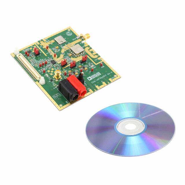
ICGOO电子元器件商城为您提供DC1747A-A由LINEAR TECHNOLOGY设计生产,在icgoo商城现货销售,并且可以通过原厂、代理商等渠道进行代购。 DC1747A-A价格参考。LINEAR TECHNOLOGYDC1747A-A封装/规格:评估和演示板和套件, LTM2882 Transceiver, RS-232 Interface Evaluation Board。您可以下载DC1747A-A参考资料、Datasheet数据手册功能说明书,资料中有DC1747A-A 详细功能的应用电路图电压和使用方法及教程。
DC1747A-A是Linear Technology(现隶属于Analog Devices)推出的一款评估板,专为LTC4020高性能多化学电池充电控制器的性能验证与开发应用而设计。该评估板主要用于便携式工业设备、医疗仪器、军用通信设备及高端消费类电子产品等需要高效、可靠电池管理系统的场景。

典型应用场景包括:便携式测试与测量仪器,这类设备要求宽输入电压范围和高效率电源管理,DC1747A-A支持9V至55V的宽输入电压,适用于多种适配器或备用电源系统;医疗手持设备,如便携超声仪或监护仪,其对电池充电精度和安全性要求极高,LTC4020具备精确的恒流/恒压调节功能,确保电池安全充放电;在太阳能储能系统中,该板可用于评估从光伏阵列向电池高效充电的方案,支持最大功率点跟踪(MPPT)功能,提升能源利用效率。

此外,DC1747A-A还适用于研发阶段的快速原型开发,工程师可通过该平台评估LTC4020在不同电池化学类型(如锂离子、磷酸铁锂、铅酸等)下的充电性能,简化设计流程,缩短产品上市周期。板载丰富的测试点和可调参数便于调试与数据采集,支持灵活配置充电电流、电压阈值和系统保护功能。

总之,DC1747A-A是一款面向工业、医疗、通信及可再生能源领域的多功能电池充电评估工具,适用于需要高性能、高可靠性电源管理解决方案的研发与验证。
| 参数 | 数值 |
| 产品目录 | 编程器,开发系统 |
| 描述 | EVALUATION LOW EM1 KIT LTM2882-3 |
| 产品分类 | |
| 品牌 | Linear Technology |
| 数据手册 | http://www.linear.com/docs/28882http://cds.linear.com/docs/39240 |
| 产品图片 |
|
| 产品型号 | DC1747A-A |
| rohs | 不适用 / 不适用 |
| 产品系列 | µModule® |
| 主要属性 | 3V 电源,双路,隔离式,收发器 + 电源 |
| 主要用途 | 接口,收发器,RS-232 |
| 产品培训模块 | http://www.digikey.cn/PTM/IndividualPTM.page?site=cn&lang=zhs&ptm=24758 |
| 使用的IC/零件 | LTM2882 |
| 其它名称 | DC1747AA |
| 嵌入式 | 否 |
| 所含物品 | 板 |
| 标准包装 | 1 |
| 相关产品 | /product-detail/zh/LTM2882IY-3%23PBF/LTM2882IY-3%23PBF-ND/2237170/product-detail/zh/LTM2882CY-5%23PBF/LTM2882CY-5%23PBF-ND/2237168/product-detail/zh/LTM2882CY-3%23PBF/LTM2882CY-3%23PBF-ND/2237167/product-detail/zh/LTM2882IY-5%23PBF/LTM2882IY-5%23PBF-ND/2237166/product-detail/zh/LTM2882IV-3%23PBF/LTM2882IV-3%23PBF-ND/2213939/product-detail/zh/LTM2882IV-5%23PBF/LTM2882IV-5%23PBF-ND/2213938/product-detail/zh/LTM2882CV-3%23PBF/LTM2882CV-3%23PBF-ND/2213937/product-detail/zh/LTM2882CV-5%23PBF/LTM2882CV-5%23PBF-ND/2213936 |
| 设计资源 | http://cds.linear.com/docs/39268 |
| 辅助属性 | - |


- 商务部:美国ITC正式对集成电路等产品启动337调查
- 曝三星4nm工艺存在良率问题 高通将骁龙8 Gen1或转产台积电
- 太阳诱电将投资9.5亿元在常州建新厂生产MLCC 预计2023年完工
- 英特尔发布欧洲新工厂建设计划 深化IDM 2.0 战略
- 台积电先进制程称霸业界 有大客户加持明年业绩稳了
- 达到5530亿美元!SIA预计今年全球半导体销售额将创下新高
- 英特尔拟将自动驾驶子公司Mobileye上市 估值或超500亿美元
- 三星加码芯片和SET,合并消费电子和移动部门,撤换高东真等 CEO
- 三星电子宣布重大人事变动 还合并消费电子和移动部门
- 海关总署:前11个月进口集成电路产品价值2.52万亿元 增长14.8%

PDF Datasheet 数据手册内容提取
DEMO MANUAL DC1747A LTM2882: Dual Isolated RS232 µModule Transceiver + Power DESCRIPTION Demonstration circuit 1747A is a dual isolated RS232 on V . The part generates the output voltage V and CC CC2 μModule® transceiver with integrated power featuring communicates all necessary signaling across the isola- the LTM®2882. The demo circuit provides a 2-chan- tion barrier using Linear Technology’s isolator μModule nel, 2500V , galvanically isolated RS232 transceiver technology. RMS interface. The demo circuit features an EMI optimized Design fi les for this circuit board are available at circuit confi guration and printed circuit board layout. All http://www.linear.com/demo components are integrated into the μModule transceiver. L, LT, LTC, LTM, Linear Technology, the Linear logo and μModule are registered trademarks of The demo circuit operates from a single external supply Linear Technology Corporation. All other trademarks are the property of their respective owners. PERFORMANCE SUMMARY (T = 25°C) A SYMBOL PARAMETER CONDITIONS MIN TYP MAX UNITS V Input Supply Range LTM2882−5 4.5 5 5.5 V CC LTM2882−3 3.0 3 3.6 V V Output Voltage LTM2882-5 I = 150mA 4.7 5 V CC2 LOAD LTM2882-3 I = 100mA 4.7 5 V LOAD f Maximum Data Rate R = 3k, C = 2.5nF 100 kbps MAX L L R = 3k, C = 1nF 250 kbps L L R = 3k, C = 250pF 1000 kbps L L V Maximum Working Insulation Voltage GND to GND2 560 V IORM DC 400 V RMS Common Mode Transient Immunity 30 kV/μs OPERATING PRINCIPLES The LTM2882 contains an isolated DC/DC converter de- The spare logic channel, DIN to DOUT, is confi gured to livering power to V at 5V from the input supply V . control the state of the driver outputs, T1OUT and T2OUT, CC2 CC Isolation is maintained by the separation of GND and GND2 by connecting DOUT to DE. where signifi cant operating voltages and transients can Data is transmitted out the driver pins T1OUT and T2OUT exist without affecting the operation of the LTM2882. The from the inputs T1IN and T2IN with the input DE set to logic side ON pin enables or shuts down the LTM2882. ON. Data is received through the receiver pins R1IN and RS232 signaling is controlled by the logic inputs T1IN, R2IN to the outputs R1OUT and R2OUT; receivers are T2IN and DE. Connection to the transceiver pins, R1IN- always active. T1OUT or R2IN-T2OUT, permits RS232 communication on the isolated side of the demo circuit. The circuit features The demo circuit has been designed and optimized for low two channels, supporting multiple RS232 channels or RF emissions. To this end, some features of the LTM2882 the addition of fl ow control on a single RS232 interface. are not available for evaluation on the demo circuit. dc1747af 1
DEMO MANUAL DC1747A OPERATING PRINCIPLES The logic supply voltage V is tied to V on the demo 3. Minimized board/ground plane size. This reduces the L CC circuit. The ON pin and the spare logic channel DIN to dipole antenna formed between the logic side and DOUT, connected to DE, are selectable by jumper pro- isolated side ground planes. gramming only. 4. Optimized top signal routing and ground fl oods to reduce EMI mitigation techniques used include the following: signal loops, minimizing differential mode radiation. 1. Four layer PCB, allowing for isolated side to logic side 5. Common mode fi ltering integrated into the input pin “bridge” capacitor. The bridge capacitor is formed be- header and output DB9 connector. Filtering helps to tween an inner layer of fl oating copper which overlaps reduce emissions caused by conducted noise and the logic side and isolated side ground planes. This minimizes the effects of cabling to common mode structure creates two series capacitors, each with ap- emissions. proximately 0.008" of insulation, supporting the full 6. A combination of low ESL and high ESR decoupling. dielectric withstand rating of 2500V . The bridge RMS A low ESL ceramic capacitor is located close to the capacitor provides a low impedance return path for module minimizing high frequency noise conduction. injected currents due to parasitic capacitances of the High ESR tantalum capacitors are included to minimize LTM2882’s signal and power isolating elements. board resonances and prevent voltage spikes due to hot 2. Discrete bridge capacitors (C3, C4) mounted between plugging of the input supply voltage. GND2 and GND. The discrete capacitors provide ad- EMI performance is shown in Figure 1, measured using ditional attenuation at frequencies below 400MHz. a Gigahertz Transverse Electromagnetic (GTEM) cell and Capacitors are safety rated type Y2, manufactured by method detailed in IEC 61000-4-20, “Testing and Mea- Murata, part #GA342QR7GF471KW01L. surement Techniques – Emission and Immunity Testing in Transverse Electromagnetic Waveguides.” 60 DETECTOR = QuasiPeak, RBW = 120kHz, 50 VBW = 300kHz, SWEEP TIME = 17s NUMBER OF POINTS = 501 40 30 m 20 V/ μ dB 10 0 –10 CISPR 22 CLASS B LIMIT –20 DC1747A-B DC1747A-A –30 0 1 2 3 4 5 6 7 8 9 10 FREQUENCY (MHz) DC1747A F01 Figure 1.DC1747A Radiated Emissions dc1747af 2
DEMO MANUAL DC1747A QUICK START PROCEDURE Demonstration Circuit 1747A is easy to set up and evalu- 5. Check for the proper output voltage. V = 5V. This CC2 ate the performance of the LTM2882. Refer to Figure 2 can be measured between probe point V2 to G2. for proper measurement equipment setup and follow the 6. Once the proper output voltages are established, con- procedure below. nect a standard 9-Pin RS232 cable between J2 on the NOTE: Use a short ground lead on the oscilloscope probe demo board and a computer. when measuring input or output voltage ripple and high 7. Launch any program with the ability to send, receive, and speed signals. monitor RS232 characters or data, including the ability 1. Install JP1 and JP2 in the ON position. to control the communication handshaking. Realterm is a free, powerful, terminal program which can easily 2. Connect jumper T1I to R1O and T2I to R2O on pin be used for the above purposes. Signals may be veri- header J1. fi ed with the use of an oscilloscope connected to any 3. With power off, connect the input power supply to VCC of the appropriate signals on pin header J1or isolated and GND on pin header J1. side probe points located next to the DB9 connector. 4. Turn on the power at the input. NOTE: Make sure that the input voltage does not exceed 6V. Figure 2. Demo Board Setup dc1747af 3
DEMO MANUAL DC1747A PCB LAYOUT Layer 1. Top Layer Layer 2. Ground Plane Layer 3. Signal Layer Layer 4. Bottom Layer PARTS LIST ITEM QTY REFERENCE DESCRIPTION MANUFACTURER/PART NUMBER Required Circuit Components 1 1 U1 I.C., LTM2882CY-3 LINEAR TECHNOLOGY LTM2882CY-3#PBF I.C., LTM2882CY-5 LINEAR TECHNOLOGY LTM2882CY-5#PBF Hardware/Components (For Demo Board Only) 2 2 C1, C5 CAP, TANT 10F 10V 20% TAJA AVX TAJA106M010RNJ 3 1 C2 CAP, CER 1F 10V 20% 0508 MURATA LLL219R71A105MA01L 4 2 C3, C4 CAP, CER 470pF 250V 10% 1808 MURATA GA342QR7GF471KW01L AC 5 1 J1 0.1" DOUBLE ROW HEADER, 5 × 2 PIN SAMTEC TSW-105-22-G-D 6 1 J1 0.1" FERRITE PLATE, 5 × 2 HOLE FAIR RITE 2644247101 7 1 J2 CON, FILTERED, DSUB 9-PIN KOBICONN 152-3609 8 2 JP1, JP2 2mm SINGLE ROW HEADER, 3-PIN SAMTEC TMM-103-02-L-S 9 2 JP1, JP2 SHUNT SAMTEC 2SN-BK-G dc1747af 4
DEMO MANUAL DC1747A SCHEMATIC DIAGRAM dc1747af 5
DEMO MANUAL DC1747A DEMONSTRATION BOARD IMPORTANT NOTICE Linear Technology Corporation (LTC) provides the enclosed product(s) under the following AS IS conditions: This demonstration board (DEMO BOARD) kit being sold or provided by Linear Technology is intended for use for ENGINEERING DEVELOPMENT OR EVALUATION PURPOSES ONLY and is not provided by LTC for commercial use. As such, the DEMO BOARD herein may not be complete in terms of required design-, marketing-, and/or manufacturing-related protective considerations, including but not limited to product safety measures typically found in finished commercial goods. As a prototype, this product does not fall within the scope of the European Union direc- tive on electromagnetic compatibility and therefore may or may not meet the technical requirements of the directive, or other regulations. If this evaluation kit does not meet the specifications recited in the DEMO BOARD manual the kit may be returned within 30 days from the date of delivery for a full refund. THE FOREGOING WARRANTY IS THE EXCLUSIVE WARRANTY MADE BY THE SELLER TO BUYER AND IS IN LIEU OF ALL OTHER WARRANTIES, EXPRESSED, IMPLIED, OR STATUTORY, INCLUDING ANY WARRANTY OF MERCHANTABILITY OR FITNESS FOR ANY PARTICULAR PURPOSE. EXCEPT TO THE EXTENT OF THIS INDEMNITY, NEITHER PARTY SHALL BE LIABLE TO THE OTHER FOR ANY INDIRECT, SPECIAL, INCIDENTAL, OR CONSEQUENTIAL DAMAGES. The user assumes all responsibility and liability for proper and safe handling of the goods. Further, the user releases LTC from all claims arising from the handling or use of the goods. Due to the open construction of the product, it is the user’s responsibility to take any and all appropriate precautions with regard to electrostatic discharge. Also be aware that the products herein may not be regulatory compliant or agency certified (FCC, UL, CE, etc.). No License is granted under any patent right or other intellectual property whatsoever. LTC assumes no liability for applications assistance, customer product design, software performance, or infringement of patents or any other intellectual property rights of any kind. LTC currently services a variety of customers for products around the world, and therefore this transaction is not exclusive. Please read the DEMO BOARD manual prior to handling the product. Persons handling this product must have electronics training and observe good laboratory practice standards. Common sense is encouraged. This notice contains important safety information about temperatures and voltages. For further safety concerns, please contact a LTC applica- tion engineer. Mailing Address: Linear Technology 1630 McCarthy Blvd. Milpitas, CA 95035 Copyright © 2004, Linear Technology Corporation dc1747af 6 Linear Technology Corporation LT 1210 • PRINTED IN USA 1630 McCarthy Blvd., Milpitas, CA 95035-7417 (408) 432-1900 ● FAX: (408) 434-0507 ● www.linear.com © LINEAR TECHNOLOGY CORPORATION 2010