ICGOO在线商城 > 集成电路(IC) > 数据采集 - ADCs/DAC - 专用型 > DAC161S997RGHT
 Datasheet下载
- 型号: DAC161S997RGHT
- 制造商: Texas Instruments
- 库位|库存: xxxx|xxxx
- 要求:
| 数量阶梯 | 香港交货 | 国内含税 |
| +xxxx | $xxxx | ¥xxxx |
查看当月历史价格
查看今年历史价格
DAC161S997RGHT产品简介:
ICGOO电子元器件商城为您提供DAC161S997RGHT由Texas Instruments设计生产,在icgoo商城现货销售,并且可以通过原厂、代理商等渠道进行代购。 DAC161S997RGHT价格参考¥15.27-¥28.37。Texas InstrumentsDAC161S997RGHT封装/规格:数据采集 - ADCs/DAC - 专用型, DAC 16 bit DSP, MICROWIRE™, QSPI™, Serial, SPI™ 16-WQFN (4x4)。您可以下载DAC161S997RGHT参考资料、Datasheet数据手册功能说明书,资料中有DAC161S997RGHT 详细功能的应用电路图电压和使用方法及教程。
DAC161S997RGHT 是由 Texas Instruments(德州仪器)生产的一款单通道、16位分辨率的数模转换器(DAC),属于数据采集中的专用型DAC。该器件采用先进的SPIm™(Serial Peripheral Interface with mWire™)接口技术,支持4线制SPI通信,并具备超低功耗特性,适用于对精度和功耗要求较高的工业应用。

主要应用场景包括:

1. 工业过程控制:广泛用于可编程逻辑控制器(PLC)、远程I/O模块及工业自动化系统中,提供高精度的模拟输出信号(如4–20 mA或0–10 V),用于驱动执行器、阀门定位器等现场设备。

2. 智能传感器与变送器:在压力、温度、流量等传感器变送器中作为核心DAC元件,实现数字控制信号到模拟电流信号的精确转换,满足工业4.0对高可靠性和高精度的需求。

3. 闭环控制系统:适用于需要精密电压或电流调节的闭环反馈系统,如电源管理、电机控制和伺服系统。

4. 电池供电设备:因其低功耗设计(工作电流仅约350 µA),适合便携式工业仪表、无线传感器节点等依赖电池长期运行的场合。

5. 功能安全系统:集成看门狗定时器、寄存器校验和故障检测机制,符合IEC 61508等工业功能安全标准,可用于安全关键型应用。

综上,DAC161S997RGHT 凭借其高精度、低功耗、强抗干扰能力和集成保护特性,特别适用于工业自动化、过程控制及智能传感等对稳定性和可靠性要求严苛的场景。
| 参数 | 数值 |
| 产品目录 | 集成电路 (IC)半导体 |
| 描述 | IC DAC 16BIT SPI/SRL 16WQFN数模转换器- DAC SPI 16B Prec DAC |
| 产品分类 | |
| 品牌 | Texas Instruments |
| 产品手册 | http://www.ti.com/litv/snas621 |
| 产品图片 |
|
| rohs | 符合RoHS无铅 / 符合限制有害物质指令(RoHS)规范要求 |
| 产品系列 | 数据转换器IC,数模转换器- DAC,Texas Instruments DAC161S997RGHT- |
| 数据手册 | |
| 产品型号 | DAC161S997RGHT |
| 产品种类 | 数模转换器- DAC |
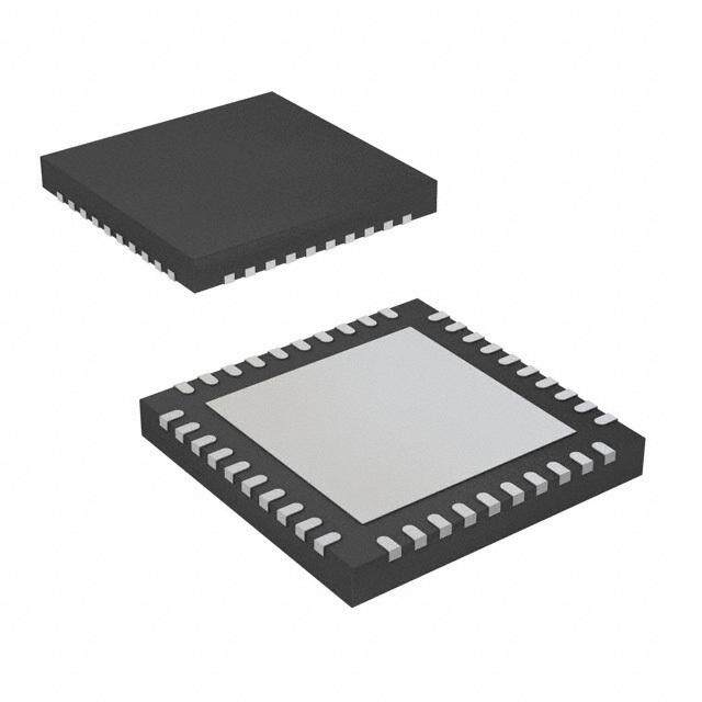
| 供应商器件封装 | 16-WQFN(4x4) |
| 其它名称 | 296-36425-1 |
| 分辨率 | 16 bit |
| 分辨率(位) | 16 b |
| 包装 | 剪切带 (CT) |
| 商标 | Texas Instruments |
| 安装类型 | 表面贴装 |
| 安装风格 | SMD/SMT |
| 封装 | Reel |
| 封装/外壳 | 16-WFQFN 裸露焊盘 |
| 封装/箱体 | WQFN-16 |
| 工作温度 | -40°C ~ 105°C |
| 工厂包装数量 | 250 |
| 接口类型 | SPI |
| 数据接口 | DSP,MICROWIRE™,QSPI™,串行,SPI™ |
| 最大工作温度 | + 105 C |
| 最小工作温度 | - 40 C |
| 标准包装 | 1 |
| 电压-电源 | 2.7 V ~ 3.6 V |
| 电压源 | 模拟和数字 |
| 电源电压-最大 | 3.6 V |
| 电源电压-最小 | 2.7 V |
| 类型 | DAC |
| 系列 | DAC161S997 |
| 转换器数量 | 1 |
| 输出类型 | Current |
| 采样率(每秒) | * |


- 商务部:美国ITC正式对集成电路等产品启动337调查
- 曝三星4nm工艺存在良率问题 高通将骁龙8 Gen1或转产台积电
- 太阳诱电将投资9.5亿元在常州建新厂生产MLCC 预计2023年完工
- 英特尔发布欧洲新工厂建设计划 深化IDM 2.0 战略
- 台积电先进制程称霸业界 有大客户加持明年业绩稳了
- 达到5530亿美元!SIA预计今年全球半导体销售额将创下新高
- 英特尔拟将自动驾驶子公司Mobileye上市 估值或超500亿美元
- 三星加码芯片和SET,合并消费电子和移动部门,撤换高东真等 CEO
- 三星电子宣布重大人事变动 还合并消费电子和移动部门
- 海关总署:前11个月进口集成电路产品价值2.52万亿元 增长14.8%


PDF Datasheet 数据手册内容提取
Product Sample & Technical Tools & Support & Folder Buy Documents Software Community DAC161S997 SNAS621A–JUNE2013–REVISEDDECEMBER2014 DAC161S997 16-Bit SPI-Programmable DAC for 4-20 mA Loops 1 Features 3 Description • 16-BitResolution The DAC161S997 is a very low power 16-bit ΣΔ 1 digital-to-analog converter (DAC) for transmitting an • Very-LowSupplyCurrentof100µA analog output current over an industry standard 4-20 • 5ppmFS/°CGainError mA current loop. The DAC161S997 has a simple 4- • Pin-ProgrammablePower-UpCondition wire SPI for data transfer and configuration of the DAC functions. To reduce power and component • Loop-ErrorDetectionandReporting count in compact loop-powered applications, the • ProgrammableOutput-CurrentErrorLevels DAC161S997 contains an internal ultra-low power • SimpleHARTModulatorInterfacing voltage reference and an internal oscillator. The low power consumption of the DAC161S997 results in • HighlyIntegratedFeatureSetinSmallFootprint additional current being available for the remaining WQFN-16(4- ×4-mm,0.5-mmPitch) portion of the system. The loop drive of the DAC161S997 interfaces to a Highway Addressable 2 Applications Remote Transducer (HART) modulator, allowing • Two-Wire4-to20-mACurrent-LoopTransmitter injection of FSK modulated digital data into the 4-20 mA current loop. This combination of specifications • Loop-PowerTransmitters andfeaturesmakestheDAC161S997idealfor2-and • IndustrialProcessControl 4-wire industrial transmitters. The DAC161S997 is • ActuatorControl available in a 16-pin 4-mm × 4-mm WQFN package and is specified over the extended industrial temperaturerangeof –40°Cto+105°C. DeviceInformation(1) PARTNUMBER PACKAGE BODYSIZE(NOM) DAC161S997 WQFN(16) 4.00mmx4.00mm (1) For all available packages, see the orderable addendum at theendofthedatasheet. 4 Simplified Schematic LOOP+ LDO VD VA Internal 4-20 mA SCLK Reference Loop CSSDBI S P I 16 ÐÂ DACIDAC +- BASE COMD SDO VD COMA 80k 40 DAC161S997 OUT ERRB LOOP- NC C1 C2 C3 ERRLVL HART Modulator 1 An IMPORTANT NOTICE at the end of this data sheet addresses availability, warranty, changes, use in safety-critical applications, intellectualpropertymattersandotherimportantdisclaimers.PRODUCTIONDATA.
DAC161S997 SNAS621A–JUNE2013–REVISEDDECEMBER2014 www.ti.com Table of Contents 1 Features.................................................................. 1 8.3 FeatureDescription...................................................8 2 Applications........................................................... 1 8.4 DeviceFunctionalModes..........................................9 3 Description............................................................. 1 8.5 Programming..........................................................10 8.6 RegisterMaps.........................................................13 4 SimplifiedSchematic............................................. 1 9 ApplicationandImplementation........................ 17 5 RevisionHistory..................................................... 2 9.1 ApplicationInformation............................................17 6 PinConfigurationandFunctions......................... 3 9.2 TypicalApplication .................................................23 7 Specifications......................................................... 4 10 PowerSupplyRecommendations..................... 29 7.1 AbsoluteMaximumRatings......................................4 11 Layout................................................................... 29 7.2 ESDRatings ............................................................4 11.1 LayoutGuidelines.................................................29 7.3 RecommendedOperatingConditions.......................4 11.2 LayoutExample....................................................29 7.4 ThermalInformation..................................................4 12 DeviceandDocumentationSupport................. 31 7.5 ElectricalCharacteristics...........................................5 7.6 TimingRequirements ...............................................6 12.1 Trademarks...........................................................31 7.7 TypicalCharacteristics..............................................7 12.2 ElectrostaticDischargeCaution............................31 12.3 Glossary................................................................31 8 DetailedDescription.............................................. 8 13 Mechanical,Packaging,andOrderable 8.1 Overview...................................................................8 Information........................................................... 31 8.2 FunctionalBlockDiagram.........................................8 5 Revision History ChangesfromOriginal(June2013)toRevisionA Page • AddedESDRatingstable,FeatureDescriptionsection,DeviceFunctionalModes,ApplicationandImplementation section,PowerSupplyRecommendationssection,Layoutsection,DeviceandDocumentationSupportsection,and Mechanical,Packaging,andOrderableInformationsection ................................................................................................. 1 2 SubmitDocumentationFeedback Copyright©2013–2014,TexasInstrumentsIncorporated ProductFolderLinks:DAC161S997
DAC161S997 www.ti.com SNAS621A–JUNE2013–REVISEDDECEMBER2014 6 Pin Configuration and Functions RGHPackage 16-PinWQFN (TopView) E S BA VA C1 C2 6 5 4 3 1 1 1 1 COMA 1 12 C3 COMD 2 11 NC DAP=COMA VD 3 10 ERRLVL SCLK 4 9 OUT 5 6 7 8 SDI CSB ERRB SDO PinFunctions PIN TYPE(1) DESCRIPTION NAME NO. BASE 16 A ExternalNPNbasedrive COMA 1 P Analog-blocknegativesupplyrail(localCOMMON) COMD 2 P Digital-blocknegativesupplyrail(localCOMMON) CSB 6 I SPIchipselect C1 14 A Externalcapacitor C2 13 A Externalcapacitor,HARTinput C3 12 A Externalcapacitor EERB 7 O Errorflagoutput,opendrain,activeLOW ERRLVL 10 I Setsoutput-currentlevelatpowerupandunder-errorconditions. NC 11 – Donotconnecttothispin. OUT 9 A Loopoutputcurrentsourceoutput SCLK 4 I SPIclockinput SDI 5 I SPIdatainput SDO 8 O SPIdataoutput VA 15 P Analog-blockpositivesupplyrail VD 3 P Digital-blockpositivesupplyrail. DAP DAP P Dieattachpad.ConnectdirectlytolocalCOMMON(COMA,COMD). (1) G=Ground,I=DigitalInput,O=DigitalOutput,P=Power,A=Analog Copyright©2013–2014,TexasInstrumentsIncorporated SubmitDocumentationFeedback 3 ProductFolderLinks:DAC161S997
DAC161S997 SNAS621A–JUNE2013–REVISEDDECEMBER2014 www.ti.com 7 Specifications 7.1 Absolute Maximum Ratings(1) MIN MAX UNIT Supplyvoltage(VA,VDtoCOMA,COMD) –0.3 6 V Voltagebetweenanytwopins(2) 6 V CurrentINorOUTofanypin—exceptOUTpin(3) 5 mA OutputcurrentatOUT 50 mA JunctionTemperature 150 °C OperatingTemperature –40 105 °C Storagetemperature,T –65 150 °C stg (1) StressesbeyondthoselistedunderAbsoluteMaximumRatingsmaycausepermanentdamagetothedevice.Thesearestressratings only,andfunctionaloperationofthedeviceattheseoranyotherconditionsbeyondthoseindicatedunderRecommendedOperating Conditionsisnotimplied.Exposuretoabsolute-maximum-ratedconditionsforextendedperiodsmayaffectdevicereliability. (2) AllvoltagesaremeasuredwithrespecttoCOMA=COMD=0V,unlessotherwisespecified. (3) Whentheinputvoltage(VIN)atanypinexceedspowersupplies(VIN<COMAorVIN>VA),thecurrentatthatpinmustnotexceed5 mA,andthevoltage(VIN)atthatpinrelativetoanyotherpinmustnotexceed6V.SeeforPinDescriptionsforadditionaldetailsof inputstructures. 7.2 ESD Ratings VALUE UNIT V Electrostaticdischarge Human-bodymodel(HBM),perANSI/ESDA/JEDECJS-001(1)(2) 2000 V (ESD) (1) JEDECdocumentJEP155statesthat500-VHBMallowssafemanufacturingwithastandardESDcontrolprocess. (2) TheHumanBodyModel(HBM)isa100pFcapacitorchargedtothespecifiedvoltagethendischargedthrougha1.5kΩresistorinto eachpin. 7.3 Recommended Operating Conditions MIN MAX UNIT BASEloadtoCOMA 0 15 pF (COMA-COMD) 0 V OUTloadtoCOMA none (VA-VD) 0 V VA,VDD Supplyvoltage 2.7 3.6 V T Temperature –40 105 °C A 7.4 Thermal Information DAC161S997 WQFN UNIT 16PINS R Packagethermalimpedance(1) 35 °C/W θJA (1) ThepackagethermalimpedanceiscalculatedinaccordancewithJESD51-7. 4 SubmitDocumentationFeedback Copyright©2013–2014,TexasInstrumentsIncorporated ProductFolderLinks:DAC161S997
DAC161S997 www.ti.com SNAS621A–JUNE2013–REVISEDDECEMBER2014 7.5 Electrical Characteristics Unlessotherwisenoted,thesespecificationsapplyforVA=VD=3.3V,COMA=COMD=0V,T =25°C,externalbipolar A transistor:2N3904,RE=22Ω,C1=C2=C3=2.2nF. PARAMETER TESTCONDITIONS MIN(1) TYP MAX(1) UNIT POWERSUPPLY VA,VD Supplyvoltage VA=VD 2.7 3.6 V -40°C≤T ≤105°C A VAsupplycurrent DACCODE=0x0200(2) 43 µA VDsupplycurrent 57 µA ICC Totalsupplycurrent 100 125 µA DCACCURACY N Resolution 16 bits INL Integralnon-linearity(3) 0x2AAA<DACCODE<0xD555 –1.5 2.6 µA (4mA<I <20mA) LOOP DNL Differentialnon-linearity see (4) –0.2 0.2 µA TUE Totalunadjustederror 0x2AAA<DACCODE<0xD555 0.01 %FS OE Offseterror see (5) –7.86 0.84 7.86 µA ΔOE Offseterrortemperaturecoefficient -40°C≤T ≤105°C 0.48 ppmFS/°C A GE Gainerror see (6) 0.007 %FS ΔGE Gainerrortemperaturecoefficient -40°C≤T ≤105°C 5 ppmFS/°C A IERRL LOWERRORcurrent ERR_LOW=default 3.36 3.375 3.39 mA IERRH HIGHERRORcurrent ERR_HIGH=default 21.70 21.75 21.82 mA LTD Longtermdrift—meanshiftof12 90 ppmFS mAoutputcurrentafter1000hours at150°C LOOPCURRENTOUTPUT(OUT) I Minimumoutputcurrent TestedatDACCODE=0x01C2(7) 0.19 mA OUTMIN I Maximumoutputcurrent TestedatDACCODE=0xFFFF 23.95 mA OUTMAX R Outputimpedance 200 MΩ OUT COMAtoOUTvoltagedrop I =24mA 960 mV OUT BASEOUTPUT I BASEshortcircuitoutputcurrent BASEforcedtoCOMApotential 10 mA OUTSC DYNAMICCHARACTERISTICS Outputnoisedensity 1kHz 20 nA/rtHz Integratedoutputnoise 1Hzto1kHzband 300 nA RMS INTERNALTIMER TM Timeoutperiod DefaultsettingofTIMEOUTin 100 ms CONFIGregister DIGITALINPUTCHARACTERISTICS I Digitalinputleakagecurrent –10 10 µA IN V Inputlowvoltage 0.2×VD V IL V Inputhighvoltage 0.7×VD V IH C Inputcapacitance 5 pF IN (1) Limitsareensuredbytesting,design,orstatisticalanalysisat25°C.Limitsovertheoperatingtemperaturerangeareensuredthrough correlationsusingstatisticalqualitycontrol(SQC)method. (2) Atcode0x0200theBASEcurrentisminimal,forexample,devicecurrentcontributiontopowerconsumptionisminimized.SPIis inactive,forexample,aftertransmittingcode0x200totheDAC161S997,therearenomoretransitionsinthechannelduringthesupply currentmeasurement. (3) INLismeasuredusingthebest-fitmethodintheoutputcurrentrangeof4mAto20mA. (4) Specifiedbydesign. (5) Offsetisthey-interceptofthestraightlinedefinedby4mAand20mApointsofthemeasuredtransfercharacteristic. (6) GainErroristhedifferenceinslopeofthestraightlinedefinedbymeasured4mAand20mApointsoftransfercharacteristic,andthat oftheidealcharacteristic. (7) ThismustbetreatedastheminimumLOOPcurrentensuredinself-poweredmode. Copyright©2013–2014,TexasInstrumentsIncorporated SubmitDocumentationFeedback 5 ProductFolderLinks:DAC161S997
DAC161S997 SNAS621A–JUNE2013–REVISEDDECEMBER2014 www.ti.com Electrical Characteristics (continued) Unlessotherwisenoted,thesespecificationsapplyforVA=VD=3.3V,COMA=COMD=0V,T =25°C,externalbipolar A transistor:2N3904,RE=22Ω,C1=C2=C3=2.2nF. PARAMETER TESTCONDITIONS MIN(1) TYP MAX(1) UNIT DIGITALOUTPUTCHARACTERISTICS V OutputLowvoltage I =200μA 0.4 V OL sink V OutputHIGHvoltage I =200μA 2.6 V OH sink I ,I TRI-STATEleakagecurrent –10 10 µA OZH OZL C TRI-STATEoutputcapacitance 5 pF OUT 7.6 Timing Requirements MIN NOM MAX UNIT f SCLKfrequency 0 10 MHz CLK t SCLKhightime 0.4/F 50 ns H CLK t SCLKlowtime 0.4/F 50 ns L CLK t CSBpulsewidth 5 40 ns CSB t CSBset-uptimepriortoSCLKrisingedge 5 ns CSS t 24thrisingedgeofSCLKtoCSBrisingedge 15 ns SCH t CSBholdtimeafterthe24thfallingedgeofSCLK 6 10 ns CSH t CSBfallingedgetoSDOvalid 10 35 ns ZSDO t CSBrisingedgetoSDOHiZ 10 ns SDOZ t SDIdataset-uptimepriortoSCLKrisingedge 10 ns DS t SDIdataholdtimeafterSCLKrisingedge 6 10 ns DH t SDOoutputdatavalid 30 ns DO Figure1. SPITimingDiagrams 6 SubmitDocumentationFeedback Copyright©2013–2014,TexasInstrumentsIncorporated ProductFolderLinks:DAC161S997
DAC161S997 www.ti.com SNAS621A–JUNE2013–REVISEDDECEMBER2014 7.7 Typical Characteristics Unlessotherwisenoted,datapresentedherewascollectedundertheseconditionsVA=VD=3.3V,T =25°C,external A bipolartransistor:2N3904,RE=22Ω,C1=C2=C3=2.2nF. 6 0 A(rms) 5 IInntteeggrraattiioonn BBWW==110kHkHzz dB) -10 (cid:29)PPLE 4 ONSE ( --3200 T RI 3 ESP -40 N R TPUT CURRE 12 MAGNITUDE ---765000 CHC1A1==RCCT22 A==dCCa33p==t21a.nt2ioFnnF U O 0 -80 0 4 8 12 16 20 24 1 10 100 1k 10k 100k OUTPUT CURRENT (mA) FREQUENCY (Hz) Figure2.IntergratedNoisevsILOOP Figure3.ΣΔModulatorFilterResponse 1M 2.5 2.0 100k 1.5 s) (cid:29)ME (10k A) 01..50 MMianx I NINLL G TI1k (cid:29)L ( 0.0 N N LI I -0.5 ETT100 -1.0 S -1.5 10 C1=C2=C3=2.2nF HART Adaptation -2.0 C1=C2=C3=1nF 1 -2.5 1 10 100 1k 10k 100k -40 -20 0 20 40 60 80 100 120 INPUT CODE STEP (lsb) TEMPERATURE (°C) Figure4.SettlingTimevsInputStepSize Figure5.OutputLinearityvsTemperature 120 120 C1=C2=C3=1nF C1=C2=C3=1nF C1=C2=C3=2.2nF C1=C2=C3=2.2nF 100 C1=C2=C3=10nF 100 C1=C2=C3=10nF C1=C2=C3=100nF C1=C2=C3=100nF 80 80 B) B) d d R ( 60 R ( 60 R R S S P P 40 40 20 20 0 0 1 10 100 1k 10k 100k 1M 1 10 100 1k 10k 100k 1M FREQUENCY (Hz) FREQUENCY (Hz) Figure6.PSRR:I =4mA Figure7.PSRR:I =20mA LOOP LOOP Copyright©2013–2014,TexasInstrumentsIncorporated SubmitDocumentationFeedback 7 ProductFolderLinks:DAC161S997
DAC161S997 SNAS621A–JUNE2013–REVISEDDECEMBER2014 www.ti.com 8 Detailed Description 8.1 Overview The DAC161S997 is a 16-bit DAC realized as a ∑Δ modulator. The DAC’s output is a current pulse train that is filtered by the on-board low pass RC filter. The final output current is a multiplied copy of the filtered modulator output. This architecture ensures an excellent linearity performance, while minimizing power consumption of the device. The DAC161S997 eases the design of robust, precise, long-term stable industrial systems by integrating all precision elements on-chip. Only a few external components are needed to realize a low-power, high-precision industrial4-20mAtransmitter. In case of a fault, or during initial power-up the DAC161S997 will output current in either upper or lower error current band. The choice of band is user selectable via a device pin. The error current value is user programmableviaSPI. 8.2 Functional Block Diagram Industrial 4-20mA Transmitter LOOP+ LDO VD VA Internal SCLK Reference 0-24 mA Loop LOOP SUPPLY + Sensor IN SDI ÐÂ DAC + - SPI SDO S P I 16 IDAC - BASE µC CSB COMD LOOP VD COMA RECEIVER 80k 40 INT ERRB DAC161S997 OUT LOOP- NC C1 C2 C3 ERRLVL HART Modulator 8.3 Feature Description 8.3.1 ErrorDetectionAndReporting Bydefault,theDAC161S997detectsandreportsseveraltypesoferrors. 8.3.1.1 LoopError A loop error occurs when the device is unable to sustain the required output current at OUT pin, typically caused byadropinloopsupply,oranincreaseinloadimpedance. When a loop error occurs, the DAC161S997 changes the OUT-pin current to the value in the ERROR_LOW register, unless the MASK_LOOP_ERR is set to 1. If the MASK_LOOP_ERR is not set, then the device also periodically attempts to reassert the OUT current set in DACCODE by default. If the DACCODE-current output is set, the DAC161S997 then stops reporting a loop error. The interval between reasserts is controlled by the L_RETRY_TIME field in the ERROR_CONFIG register. If the DIS_RETRY_LOOP field in the ERROR_CONFIG register is changed to 1, the device does not periodically check the loop and, instead, only checks the loop after areadoftheERR_STATUS(0x09)register.Ifthelooperrorisnotresolved,thentheloop-errorcurrentpersists. 8 SubmitDocumentationFeedback Copyright©2013–2014,TexasInstrumentsIncorporated ProductFolderLinks:DAC161S997
DAC161S997 www.ti.com SNAS621A–JUNE2013–REVISEDDECEMBER2014 Feature Description (continued) When a loop error occurs, the DAC161S997 sets the CURR_LOOP_STATUS and LOOP_STATUS fields in the STATUS register to 1. The LOOP_STATUS field remains set to 1 until the STATUS register is read or the device is reset. If the loop error is cleared, either by the device reasserting the loop current or by changing the OUT current,thentheCURR_LOOP_STATUSfieldclears. 8.3.1.2 SPITimeoutError(ChannelError) The DAC161S997 expects to receive periodic SPI write commands to ensure that the SPI connection is functioning normally. If no SPI write command occurs within the time indicated by the SPI_TIMEOUT field in the ERROR_CONFIG register, the device reports a SPI timeout error. Note that the SPI write command must be properly formatted to avoid SPI Timeout errors (such as a write command that generates a frame error does not preventanimminentSPITimeouterror). SPI Timeout error reporting is inhibited by MASK_SPI_TOUT. SPI Timeout errors are not reported on the loop if MASK_SPI_ERRissetto1. Note that a write command to address 0 is not considered a valid write command and will not prevent a SPI Timeouterror. 8.3.1.3 FrameError If a SPI write command has an incorrect number of SCLK pulses, the device reports a frame error. The number of SCLK pulses must be an integer and a multiple of 24. A frame error is always reported by ERRB being pulled low.Aframeerrordoesnotaffecttheloopcurrent. 8.3.1.4 AlarmCurrent By default, the DAC161S997 reports faults to the plant controller by forcing the OUT current into one of two error bands. The error current bands are defined as either greater than 20 mA, or less than 4 mA. Loop errors are reportedbysettingcurrentofERR_LOW. If SPI Timeout Errors are reported on the loop (this is the default; it can be changed by setting the register ERR_CONFIG:MASK_LOOP_ERR), the error band is controlled by the ERRLVL pin. When ERRLVL is tied to the COMD voltage, the ERR_LOW current is the reporting current. If ERRLVL is tied to VD then the ERR_HIGH currentisthecurrent-onpin,OUT,ifaSPItimeouterroroccurs. The exact value of the output current used to indicate fault is dictated by the contents of ERR_HIGH and ERR_LOWregisters. In the case of a conflicting alarm-current setting (such as a loop error and SPI timeout error occurring simultaneouslyandERRLVListiedhigh),thecurrent-onpin,OUT,isdeterminedbyERR_LOWcurrent. 8.4 Device Functional Modes The DAC161S997 reports errors in 3 different ways, by changing the OUT pin current, pulling the ERRB pin low, and by updating the read-only register STATUS. The reporting on ERRB and OUT pin is customized by setting theERROR_CONFIGregister. TheERRBpinconnectstoaGPIOpinonthemicrocontrollertofunctionasaninterruptifanerroroccurs. If a Loop error and a SPI Timeout error occur simultaneously and the device is configured with conflicting error outputcurrents,theOUTpincurrentreportstheLoopError. STATUSRegister LoopReporting ERRBReporting FrameError ReportedinFERR_STS Notreported Alwaysreported Reportedbydefaultunless Reportedbydefaultunless ReportedinLOOP_STSand LoopError ERR_CONFIG:MASK_LOOP_E ERR_CONFIG:DIS_LOOP_ERR_ERRB CURR_LOOP_STS RRissetto1 issetto1 Reportedbydefaultunlesseither ERR_CONFIG:MASK_SPI_ERR Reportedbydefaultunless SPITimeoutError ReportedinSPI_TIMEOUT_ERR or ERR_CONFIG:MASK_SPI_TOUTisset ERR_CONFIG:MASK_SPI_TOU to1 Taresetto1 Copyright©2013–2014,TexasInstrumentsIncorporated SubmitDocumentationFeedback 9 ProductFolderLinks:DAC161S997
DAC161S997 SNAS621A–JUNE2013–REVISEDDECEMBER2014 www.ti.com 8.5 Programming 8.5.1 SerialInterface The 4-wire interface is compatible with SPI, QSPI, and MICROWIRE, as well as most DSPs. See the Timing Requirements section for timing information about the read and write sequences. The serial interface is comprised of CSB, SCLK, SDIs and SDO. The DAC161S997 supports both Mode 0 and Mode 3 of the SPI protocol. A bus transaction is initiated by the falling edge of CSB. When CSB is low, the input data is sampled at the SDI pinbytherisingedgeoftheSCLK.TheoutputdataisassertedontheSDOpinatthefallingedgeofSCLK. Avalidtransferrequiresanintegermultipleof24SCLKcycles.IfCSBisraisedbeforethe24thrisingedgeofthe SCLK, the transfer aborts and a Frame Error is reported. If CSB is held low after the 24th falling edge of the SCLK and additional SCLK edges occur, the data continues to flow through the FIFO and out the SDO pin. When CSB transitions high, the internal controller decodes the most recent 24 bits that were received before the rising edge of CSB. CSB must transition to high after an integer multiple of 24 clock cycles, otherwise a Frame Error is reported and the transaction is considered invalid. When a valid number of SCLK pulses occur with CSB low,theDACthenperformstherequestedoperationafterCSBtransitionshigh. Figure8. SPIDataFormat The acquired data is shifted into an internal 24-bit shift register (MSB first) which is configured as a 24-bit deep FIFO. As the data is being shifted into the FIFO via the SDI pin, the prior contents of the register are being shiftedoutthroughtheSDOoutput.WhileCSBishigh,SDOisinahighZ-state.AtthefallingedgeofCSB,SDO presents the MSB of the data present in the shift register. SDO is updated on every subsequent falling edge of SCLK. NOTE The first SDO transition will happen on the first falling edge AFTER the first rising edge of SCLKwhenCSBislow. The 24 bits of data contained in the FIFO are interpreted as an 8-bit COMMAND word followed by 16-bits of DATA. The general format of the 24-bit data stream is shown in Figure 9. Complete instruction set is tabulated in theDetailedDescriptionsection. Figure9. SPICommandandDataWords 10 SubmitDocumentationFeedback Copyright©2013–2014,TexasInstrumentsIncorporated ProductFolderLinks:DAC161S997
DAC161S997 www.ti.com SNAS621A–JUNE2013–REVISEDDECEMBER2014 Programming (continued) 8.5.1.1 SPIWrite SPI write operation is used to change the state of the device. Handshaking does not occur between the master and the slave (DAC161S997), and the master must control the communication on the following inputs: SCLK, CSB,SDI.TheformatofthedatatransferisdescribedintheSerialInterface section. A write is composed of two sections, 8-bits corresponding to a command and 16-bits of data. A command is simply the address of the desired register to update. Note that some registers are read-only; a write to these registers will have no effect on the device operation and the register contents will not change. The user instructionsetisshownintheDetailedDescriptionsection. During power up or device reset, the register contents of all writable registers are set to the listed values in the DetailedDescriptionsection. If the DAC161S997 is used in a highly noisy environment in which SPI errors are potentially an issue, the DAC161S997supportsamorerobustprotocol(seeOptionalProtectedSPIWrites). 8.5.1.2 SPIRead The read operation requires all 4 wires of the SPI interface, which are SCLK, SCB, SDI, and SDO. The simplest READ operation occurs automatically during any valid transaction on the SPI bus because the SDO pin of DAC161S997 always shifts out the contents of the internal FIFO. Therefore the data being shifted in to the FIFO is verified by initiating another transaction and acquiring data at SDO, allowing only for the verification of FIFO contents. The internal registers are accessed by the user through a register read command. A register read command is formed by setting bit 7 of the command to 1 (effectively ORing with 0x80) with the address of the desired register to be read and sending the resulting 8 bits as the command (see Detailed Description). For example, the register readcommandoftheSTATUSregister(address0x05)wouldbe0x85. A register read requires two SPI transactions to recover the register data. The first transaction shifts in the register read command; an 8-bits of command byte followed by 16-bits of dummy data. The register read command transfers the contents of the internal register into the FIFO. The second transaction shifts out the FIFO contents; an 8-bit command byte (which is a copy of previous transaction) followed by the register data. The RegisterReadoperationisshowninFigure10. Figure10. SPIRegisterReadOperation 8.5.1.3 OptionalProtectedSPIWrites TheDAC161S997supportsanoptionalSPIprotocolintendedtoproviderobustsupportagainstSPIwriteerrors. WhenPROTECT_REG_WRissetto1,allregisterwritesrequireasubsequentXFER_REGcommand(awriteof 0x00FF to XFER_REG[0x01]) to load the transferred data into the register address (see Figure 11). This requirementprovidesprotectionagainstwriteerrorsinanelectricallynoisyenvironment. Copyright©2013–2014,TexasInstrumentsIncorporated SubmitDocumentationFeedback 11 ProductFolderLinks:DAC161S997
DAC161S997 SNAS621A–JUNE2013–REVISEDDECEMBER2014 www.ti.com Programming (continued) SPI Write n Register Load CSB SCLK 1 2 8 9 24 1 2 8 9 24 SDI Addr n Data n XFER_REG 0x00FF Prior Addr Prior Data Addr n Data n SDO Figure11. ProtectedSPIwrites 8.5.1.3.1 SPIWriteErrorCorrection To minimize the chance of a SPI write error, TI recommends to append a NOP command onto the end of every registerwritesequencetoverifythattheXFER_REGisproperlyexecuted,asshowninFigure12. SPI Write n Register Load NOP CSB SCLK 1 2 8 9 24 1 2 8 9 24 1 2 8 9 24 SDI Addr n Data n XFER_REG 0x00FF NOP 0xXXXX SDO Prior Addr Prior Data Addr n Data n XFER_REG 0x00FF Figure12. ProtectedSPIwriteswithNOPcommand The XFER_REG command combined with the automatic SDO loopback of the previous SPI write data prevents loading of incorrect data into a register. If the loopback indicates a communication error has occurred (see Figure 13), the CSB pin is held low and the previous write command is repeated. Although the second SPI transaction had 48 SCLK pulses instead of 24 pulses, this is not considered a frame error. A frame error is indicatedwhenthenumberofSCLKpulsesisnotanintegermultipleof24. 12 SubmitDocumentationFeedback Copyright©2013–2014,TexasInstrumentsIncorporated ProductFolderLinks:DAC161S997
DAC161S997 www.ti.com SNAS621A–JUNE2013–REVISEDDECEMBER2014 Programming (continued) Register Load ± Error Detected Data ORKe, speunlld C RSeBg ihsitgehr Ltoo acodmplete SPI Write n Repeat Write n operation NOP Do Not pull CSB high CSB SCLK 1 2 8 9 24 1 2 8 9 24 2526 48 1 2 8 9 24 1 2 8 9 24 SDI Addr n Data n XFER_REG 0x00FF Addr n Data n XFER_REG 0x00FF NOP 0xXXXX Communication Error Error reported to MCU SDO Prior Addr Prior Data Addr n Data n XFER_REG 0X00FF Addr n Data n XFER_REG 0x00FF Figure13. DetectionofErrorinRegisterLoad If a communication error occurs in the XFER_REG command, it is detected during the trailing NOP command (see Figure 14). Although the register load is incomplete, the device has not changed operations. Repeat the originaldataandXFER_REGcommand. SPI Write n Register Load NOP SPI Write n Register Load NOP CSB SCLK 12 8 9 24 12 8 9 24 12 8 9 24 12 8 9 24 12 8 9 24 12 8 9 24 SDI Addr n Data n XFER_REG 0x00FF Addr n Data n Addr n Data n XFER_REG 0x00FF NOP 0xXXXX Communication Error Error reported to MCU SDO Prior Addr Prior Data Addr n Data n XFER_REG? 0x00FF? Prior Addr Prior Data Addr n Data n XFER_REG 0x00FF Figure14. DetectionofErrorinRegisterReadback 8.6 Register Maps Unless otherwise indicated, bits outside the register fields listed below are do not care, and will not change device configuration. Register read operations on such do not care fields will be 0. Registers are read/write unlessindicatedotherwise. Table1.XFER_REG(WriteOnly) Address=0x01 BitField FieldName Description WhenPROTECT_REG_WRissetto1,thenaXFER_REGcommandisnecessaryto 15:0 XFER[15:0] transferthepreviousregisterwritedataintotheappropriateaddress.Setthisregister to0x00FFtoperformaXFER_REGcommand. Table2.NOP Address=0x02 BitField FieldName Description NoOperation.Awritetothisregisterwillnotchangeanydeviceconfiguration. 15:0 NOP[15:0] ThiscommandindicatesthattheSPIconnectionisfunctioningandisusedtoavoid SPI_INACTIVEerrors. Copyright©2013–2014,TexasInstrumentsIncorporated SubmitDocumentationFeedback 13 ProductFolderLinks:DAC161S997
DAC161S997 SNAS621A–JUNE2013–REVISEDDECEMBER2014 www.ti.com Table3.WR_MODE Address=0x03;Default=0x0000 BitField FieldName Description 0:RegisterwritedatatransferstoappropriateaddressimmediatelyafterCSBgoes high.Defaultvalue. 0 PROTECT_REG_WR 1:Enableprotectedregistertransfers:allregisterwritesrequireasubsequent XFER_REGcommandtofinalizetheloadingofregisterdata.RefertoOptional ProtectedSPIWrites. Table4.DACCODE Address=0x04;Default=0x2400,0xE800 BitField FieldName Description 16-bitnaturalbinaryword,whereD15istheMSB,whichindicatesthedesiredDAC outputcode. 15:0 DACCODE[15:0] NotethedefaultvalueofthisregisterisbasedonthestateoftheERR_LVLpinduring startuporreset. Table5.ERR_CONFIG Address=0x05;Default=0x0102 BitField FieldName Description L_RETRY_TIMEsetsthetimeintervalbetweensuccessiveattemptstoreassertthe desiredDACCODEoutputcurrentwhenalooperrorispresent.Thishasnoeffectif eitherMASK_LOOP_ERRissetto1orifDIS_RETRY_LOOPissetto1. 10:8 L_RETRY_TIME[2:0] LOOPRetrytime=(L_RETRY_TIME+1)×50ms Defaultvalue=1(100ms) 0:Whenalooperrorisoccurring,periodicallyattempttosenddesiredDACCODE outputcurrentinsteadofthesetERR_LOWcurrent.Theintervalbetweenattemptsis 7 DIS_RETRY_LOOP setbyL_RETRY_TIMER.Defaultvalue. 1:DonotperiodicallyreassertDACCODEoutputwhenalooperrorispresent; reassertDACCODEafterSTATUSRegisterisreadout. 0:WhenaLOOPerrorisdetectedtheDAC161S997outputsthecurrentindicatedby ERR_LOWinsteadofDACCCODE.Defaultvalue. 6 MASK_LOOP_ERR 1:WhenaLoopErrorisdetectedtheDAC161S997triestomaintainDACCODE currentonpinOUT. 0:WhenaLOOPerrorisdetectedtheDAC161S997drivesERRBpinlow.Default 5 DIS_LOOP_ERR_ERRB value. 1:WhenaLOOPerrorisdetectedtheDAC161S997doesnotdriveERRBpinlow. 0:SPItimeouterrorschangetheOUTpincurrenttoanerrorvalue,whichis determinedbyERRLVLpinandcontentsofERR_LOWorERR_HIGH.Note: 4 MASK_SPI_ERR MASK_SPI_TOUTmustbesetto0forthistobereported.Defaultvalue. 1:SPItimeouterrorsdonotchangetheOUTpincurrenttoanerrorvalue. SPI_TIMEOUTsetsthetimeintervalforSPItimeouterrorreporting.AftereachSPI writecommand,aninternaltimerisreset;ifnosubsequentwriteoccursbeforethe timerreachesSPItimeout,aSPItimeouterrorisreported.SPI_ERRORreportingis inhibitedbysettingMASK_SPI_TOUT. 3:1 SPI_TIMEOUT[2:0] ANOPwriteisconsideredavalidwriteandresetsthetimerwithoutchangingthe deviceconfiguration. SPITimeout=(SPI_TIMEOUT+1)×50ms SPI_TIMEOUTdefaultvalue=1(100ms) 0:SPItimeouterrorreportingisenabled.ASPItimeouterrordrivesERRBlowwhena 0 MASK_SPI_TOUT SPITimeouterroroccurs.Defaultvalue. 1:SPItimeouterrorreportingisinhibited. 14 SubmitDocumentationFeedback Copyright©2013–2014,TexasInstrumentsIncorporated ProductFolderLinks:DAC161S997
DAC161S997 www.ti.com SNAS621A–JUNE2013–REVISEDDECEMBER2014 Table6.ERR_LOW Address=0x06;Default=0x2400 BitField FieldName Description UndersomeerrorconditionstheoutputcurrentcorrespondingtothisvalueistheDAC output,regardlessofthevalueofDACCODE.TheERR_LOWvalueisusedasthe upperbyteoftheDACCODE,whilethelowerbyteisforcedto0x00. 15:8 ERR_LOW[7:0] ERR_LOWmustbebetween0x00(0mA)and0x80(12mA).TheDAC161S997 ignoresanyvalueoutsideofthatrangeandretainsthepreviousvalueintheregister. RefertotheErrorDetectionAndReportingsectionforadditionaldetails. Thedefaultvalueis0x24,whichcorrespondstoapproximately3.37mAonpinOUT. Table7.ERR_HIGH Address=0x07;Default=0xE800 BitField FieldName Description UndersomeerrorconditionstheoutputcurrentcorrespondingtothisvalueistheDAC output,regardlessofthevalueofDACCODE.TheERR_HIGHvalueisusedasthe upperbyteoftheDACCODE,whilethelowerbyteisforcedto0x00. 15:8 ERR_HIGH[7:0] ERR_HIGHmustbegreaterthanorequalto0x80(12mA).TheDAC161S997ignores anyvaluebelow0x80andretainsthepreviousvalueintheregister.RefertotheError DetectionAndReportingsectionforadditionaldetails. Thedefaultvalueis0xE8,whichcorrespondstoapproximately21.8mAonpinOUT. Table8.RESET Address=0x08 BitField FieldName Description Write0xC33CtotheRESETregisterfollowedbyaNOPtoresetthedevice.All 15:0 RESET[15:0] writableregistersarereturnedtodefaultvalues. Table9.STATUS(Read-Only) Address=0x09or0x7F BitField FieldName Description DACresolution 7:5 DAC_RES[2:0] OnDAC161S997,returnsa111. ReturnsthestateoftheERRLVLpin: 4 ERRLVL_PIN 1=ERRLVLpinistiedHIGH 0=ERRLVLpinistiedLOW Frame-errorstatusstickybit 1=AframeerrorhasoccurredsincethelastSTATUSread. 3 FERR_STS 0=NoframeerroroccurredsincethelastSTATUSread. ThiserrorisclearedbyreadingtheSTATUSregister.Aframeerroriscausedbyan incorrectnumberofclocksduringaregisterwrite.Aregisterwritewithoutaninteger multipleof24clockcycleswillcauseaFrameerror. SPItimeouterror 1=TheSPIinterfacehasnotreceivedavalidcommandwithintheintervalsetby SPI_TIMEOUT. 2 SPI_TIMEOUT_ERR 0=TheSPIinterfacehasreceivedavalidcommandwithintheintervalsetby SPI_TIMEOUT Ifthiserroroccurs,itisclearedwithaproperlyformattedwritecommandtoavalid address. Copyright©2013–2014,TexasInstrumentsIncorporated SubmitDocumentationFeedback 15 ProductFolderLinks:DAC161S997
DAC161S997 SNAS621A–JUNE2013–REVISEDDECEMBER2014 www.ti.com Table9.STATUS(Read-Only)(continued) Address=0x09or0x7F BitField FieldName Description Loopstatusstickybit 1=AlooperrorhasoccurredsincelastreadofSTATUS. 1 LOOP_STS 0=NolooperrorhasoccurredsincelastreadofSTATUS. Returnsthelooperrorstatus.Whenthevalueinthisregisteris1,theDAC161S997is unabletomaintaintheoutputcurrentsetbyDACCODEatsomepointsincethelast STATUSread.ThisindicatorclearsafterreadingtheSTATUSregister. Currentloopstatus 1=Alooperrorisoccurring. 0 CURR_LOOP_STS 0=Nolooperrorisoccurring. ReturnsthecurrentLooperrorstatus.Whenthevalueinthisregisteris1,the DAC161S997isunabletomaintaintheoutputcurrentsetbyDACCODE. 16 SubmitDocumentationFeedback Copyright©2013–2014,TexasInstrumentsIncorporated ProductFolderLinks:DAC161S997
DAC161S997 www.ti.com SNAS621A–JUNE2013–REVISEDDECEMBER2014 9 Application and Implementation NOTE Information in the following applications sections is not part of the TI component specification, and TI does not warrant its accuracy or completeness. TI’s customers are responsible for determining suitability of components for their purposes. Customers should validateandtesttheirdesignimplementationtoconfirmsystemfunctionality. 9.1 Application Information 9.1.1 16-bitDacAndLoopDrive 9.1.1.1 DCCharacteristics The DAC converts the 16-bit input code in the DACCODE registers to an equivalent current output. The ΣΔ DAC output is a current pulse which is then filtered by a third-order RC lowpass filter and boosted to produce the loop current(I )atthedeviceOUTpin. LOOP LOOP+ VD VA IAUX DAC + BASE IDAC - ILOOP + ID IA - IE RE COMA R1 = 80k R2 = 40 I2 OUT DAC161S997 LOOP- Figure15. Loop-PoweredTransmitter Figure 15 shows the principle of operation of the DAC161S997 in the Loop-Powered Transmitter (the circuit details are omitted for clarity). In Figure 15, I and I represent supply (quiescent) currents of the internal digital D A and analog blocks. I represents supply (quiescent) current of companion devices present in the system, such AUX as the voltage regulator and the digital interface. Because both the control loop formed by the amplifier and the bipolartransistorforcethevoltageacrossR andR tobeequal,undernormalconditions,theI isdependent 1 2 LOOP onlyonI throughthefollowingrelationship(seeEquation1). DAC I =(1+R1/R2)I LOOP DAC where • I =ƒ(DACCODE) (1) DAC Although I has a number of component currents, I = I + I + I + I + I , only I is regulated by the Loop LOOP DAC D A AUX E E loop to maintain the relationship shown in Equation 1. Because only the magnitude of I is controlled, not the E direction, there is a lower limit to I . This limit is dependent on the fixed components I and I , and on system LOOP A D implementationthroughI . AUX Copyright©2013–2014,TexasInstrumentsIncorporated SubmitDocumentationFeedback 17 ProductFolderLinks:DAC161S997
DAC161S997 SNAS621A–JUNE2013–REVISEDDECEMBER2014 www.ti.com Application Information (continued) LOOP+ VD VA +- VLOCAL IAUX DAC + BASE IDAC - ILOOP + ID IA - IE RE COMA R1 = 80k R2 = 40 I2 OUT DAC161S997 LOOP- Figure16. Self-PoweredTransmitter Figure 16 shows the variant of the transmitter where the local supply provides supply currents to the system blocks, and not the 4-20mA loop Self-Powered Transmitter. The ame basic relationship between the I and LOOP I continues,butthecomponentcurrentsofI areonlyI andI . DAC LOOP DAC E 9.1.1.2 DCInput-OutputTransferFunction TheoutputcurrentsourcedbytheOUTpinofthedeviceisexpressedbyEquation2. I =24mA(DACCODE/216) (2) LOOP The valid DACCODE range is the full 16-bit code space (0x0000 to 0xFFFF), resulting in the I range of 0 to DAC approximately 12 μA, which, however, does not result in the I range of 0 to 24 mA. The maximum output LOOP current sourced out of OUT pin, I , is 24 mA. The minimum output current is dependent on the system LOOP implementation. The minimum output current is the sum of the supply currents of the DAC161S997 internal blocks, I , I , and companion devices present in the system, I . The last component current, I , is theoretically A D AUX E controlled down to 0, however, due to the stability considerations of the control loop, not allowing the I to drop E below200μAisadvised. The graph in Figure 17 shows the DC transfer characteristic of the 4-20mA transmitter, including minimum current limits. The minimum current limit for the Loop-Powered Transmitter is typically around 400 μA (I + I + D A I + I ). The minimum current limit for the Self-Powered Transmitter is typically around 200 μA (I ). Typical AUX E E valuesforI andI arelistedintheElectricalCharacteristicstable.I dependsontheBJTdeviceused. D A E 18 SubmitDocumentationFeedback Copyright©2013–2014,TexasInstrumentsIncorporated ProductFolderLinks:DAC161S997
DAC161S997 www.ti.com SNAS621A–JUNE2013–REVISEDDECEMBER2014 Application Information (continued) 24.0 21.5 Programmable IERROR 20.0 e g n a A) acy r m ur I (LOOP full acc 4.0 3.5 Programmable IERROR 0.4 MIN(ILOOP) ± Loop Powered 0.2 MIN(ILOOP) ± Self Powered 0000 0222 0444 2500 2AAA D555 E500 FFFF DACCODE (hex) Figure17. DAC-DCTransferFunction 9.1.1.3 LoopInterface The DAC161S997 cannot directly interface to the typical 4 - 20 mA loop due to the excessive loop supply voltage. The loop interface has to provide the means of stepping down the LOOP Supply to 3.6V. This can be accomplishedwitheitheralinearregulator(LDO)orswitchingregulatorwhilekeepinginmindthattheregulator’s quiescent current will have direct effect on the minimum achievable I (see DC Input-Output Transfer LOOP Function). The second component of the loop interface is the external NPN transistor (BJT). This device is part of the control circuit that regulates the transmitter’s output current (I ). Since the BJT operates over the wide current LOOP range, spanning at least 4 - 20 mA, it is necessary to degenerate the emitter in order to stabilize transistor’s transconductance (g ). The degeneration resistor of 22Ω is suggested in typical applications. For circuit details, m seeFigure21. The NPN BJT should not be replaced with an N-channel FET (Field Effect Transistor) for the following reasons: discrete FET’s typically have high threshold voltages (VT), in the order of 1.5V to 2V, which is beyond the BASE output maximum range; discrete FET’s present higher load capacitance which may degrade system stability margins;andBASEoutputreliesontheBJT’sbasecurrentforbiasing. 9.1.1.4 LoopCompliance The maximum V(LOOP+,LOOP-) potential is limited by the choice of step-down regulator, and the external BJT’s Collector Emitter breakdown voltage. For minimum V(LOOP+, LOOP−) potential consider TROUBLE Figure 16. Here, observe that V(LOOP+,LOOP−) ≅ min(V ) + I R + I R = min(V ) + 0.53V + 0.96V = 3.66V, at CE LOOP E LOOP 2 CE I =24mA.ThevoltagedropacrossinternalR isspecifiedinElectricalCharacteristics. LOOP 2 9.1.1.5 ACCharacteristics Theapproximatefrequencydependentcharacteristicsoftheloopdrivecircuitcanbeanalyzedusingthecircuitin Figure18. Copyright©2013–2014,TexasInstrumentsIncorporated SubmitDocumentationFeedback 19 ProductFolderLinks:DAC161S997
DAC161S997 SNAS621A–JUNE2013–REVISEDDECEMBER2014 www.ti.com Application Information (continued) LOOP+ DAC161S997 RX1 Gm + IAUX A(s) BASE gm ro + CX1 CX2 - - CX3 IDAC RE COMA R1 R2 CX4 OUT LOOP- Figure18. CapacitancesAffectingControlLoop Hereitisassumedthattheinternalamplifierdominatesthefrequencyresponseofthesystem,andithasasingle pole response. The BJT’s response, in the bandwidth of the control loop, is assumed to be frequency independentandischaracterizedbythetransconductanceg andtheoutputresistancer . m o As in previous sections I and I represent the filtered output of the ∑Δ modulator and the quiescent current DAC AUX ofthecompaniondevices. The circuit in Figure 18 can be further simplified by omitting the on-board capacitances, whose effect will be discussed in Stability, and by combining the amplifier, the external transistor and resistor R into one G block. E m TheresultingcircuitisshowninFigure19. ByassumingthattheBJT’soutputresistance(r )islarge,theloopcurrentI canbeexpressedas: o LOOP (3) LOOP+ ILOOP A(s)Gmve A(s)Gm + + ve ro IAUX - IDAC - R1 R2 ILOOP LOOP- Figure19. ACAnalysisModelofaTransmitter ThesumofvoltagedropsaroundthepathcontainingR ,R andv is: 1 2 e (4) Anassumptionismadeontheresponseoftheinternalamplifier: A(s) = Ao&o s (5) 20 SubmitDocumentationFeedback Copyright©2013–2014,TexasInstrumentsIncorporated ProductFolderLinks:DAC161S997
DAC161S997 www.ti.com SNAS621A–JUNE2013–REVISEDDECEMBER2014 Application Information (continued) BycombiningtheabovethefinalexpressionfortheI asafunctionof2inputsI andI is: LOOP DAC AUX ILOOP = IDAC (1 +RR21 )s +A oAGomGRm2R&2o&o + IAUXs + AoGsmR2&o 20 log (1 +R1) R2 0 dB & AoGmR2&o (6) The result above reveals that there are 2 distinct paths from the inputs I and I to the output I . I DAC AUX LOOP DAC followsthelow-pass,andtheI followsthehigh-passpath. AUX In both cases the corner frequency is dependent on the effective transconductance, G , of the external m transistor. This implies that control loop dynamics could vary with the output current I if G were allowed to LOOP m be just native device transconductance g . This undesirable behavior is mitigated by the degenerating resistor m R whichstabilizesG asfollows: E m (7) ThisresultsinthefrequencyresponsewhichislargelyindependentoftheoutputcurrentI : LOOP ILOOP = IDAC (1 +RR21 )s +A oARRoER2RE2&o&o + IAUX s + AosRRE2 &o (8) While the bandwidth of the I path may not be of great consequence given the low frequency nature of the 4- DAC 20 mA current loop systems, the location of the pole in the I path directly affects PSRR of the transmitter AUX circuit.ThisisfurtherdiscussedinPSRR. 9.1.1.5.1 StepResponse The transient input-output characteristics of the DAC161S997 are dominated by the response of the RC filter at theoutputofthe ∑Δ DAC.SettlingtimesduetostepinputareshowninTypicalCharacteristics. 9.1.1.5.2 OutputImpedance Theoutputimpedanceisdescribedas: (9) ByconsideringthecircuitinFigure19,andsettingI =I =0,thefollowingexpressioncanbeobtained: DAC AUX (10) As in AC Characteristics an assumption can be made on the frequency response of the internal amplifier, and theeffectivetransconductanceG shouldbestabilizedwithexternalR leadingto: m E (11) TheoutputimpedanceofthetransmitterisaproductoftheexternalBJT'soutputresistancer ,andthefrequency o characteristics of the internal amplifier. At low frequencies this results in a large impedance that does not significantlyaffecttheoutputcurrentaccuracy. Copyright©2013–2014,TexasInstrumentsIncorporated SubmitDocumentationFeedback 21 ProductFolderLinks:DAC161S997
DAC161S997 SNAS621A–JUNE2013–REVISEDDECEMBER2014 www.ti.com Application Information (continued) 9.1.1.5.3 PSRR Power Supply Rejection Ratio is defined as the ability of the current control loop to reject the variations in the supplycurrentofthecompaniondevices,I .Specifically: AUX (12) It was shown in AC Characteristics that the I affects I via the high-pass path whose corner frequency is AUX LOOP dependent on the effective Gm of the external BJT. If that dependence were not mitigated with the degenerating resistorR ,thePSRRwouldbedegradedatlowoutputcurrentI . E LOOP ThetypicalPSRRperformanceofthetransmittershowninFigure6 isshowninTypicalCharacteristics. 9.1.1.5.4 Stability The current control loop's stability is affected by the impedances present in the system. Figure 18 shows the simplified diagram of the control loop, formed by the on-board amplifier and an external BJT, and the lumped capacitancesC throughC thatmodelanyotherexternalelements. X1 X4 C typicallyrepresentsalocalstep-downregulator,orLDO,andanyothercompaniondevicespoweredfromthe X1 LOOP+. This capacitance reduces the stability margins of the control loop, and therefore it should be limited. RX1canbeusedtoisolateC fromLOOP+nodeandthusremedythestabilitymarginreduction.IfR =0,C X1 X1 X1 cannot exceed 10 nF. R = 200Ω is recommended if it can be tolerated. Minimum R = 40Ω if C exceeds 10 X1 X1 X1 nF. C also adversely affects stability of the loop and it must be limited to 20 pF. C affects the control loop in the X3 X4 same way as C , and it should be treated in the same way as C . C is the only capacitance that improves X1 X1 X2 stabilitymarginsofthecontrolloop.Itsmaximumsizeislimitedonlybythesafetyrequirements. Stability is a function of I as well. Since I is approximately equal to the collector current of the external LOOP LOOP BJT, G of the BJT, and thus loop dynamics, depend on I . This dependence can be reduced by m LOOP degenerating the emitter of the BJT with a small resistance as discussed in Loop Interface. Inductance in series withtheLOOP+andLOOP− donotsignificantlyaffectthecontrolloop. 9.1.1.5.5 NoiseandRipple TheoutputoftheDACisacurrentpulsetrain.ThetransitiondensityvariesthroughouttheDACinputcoderange (I range). At the extremes of the code range, the transition density is the lowest which results in low LOOP frequency components of the DAC output passing through the RC filter. Hence, the magnitude of the ripple present in I is the highest at the ends of the transfer characteristic of the device (see Typical LOOP Characteristics). It should be noted that at wide noise measurement bandwidth, it is the ripple due to the ∑Δ modulator that dominates the noise performance of the device throughout the entire code range of the DAC. This results in the “U” shaped noise characteristic as a function of output current. At narrow bandwidths, and particularly at mid- scaleoutputcurrents,itistheamplifierdrivingtheexternalBJTthatstartstodominateasanoisesource. 9.1.1.5.6 DigitalFeedthrough Digitalfeedthroughisindiscerniblefromtherippleinducedbythe∑Δmodulator. 9.1.1.5.7 HARTSignalInjection TheHARTspecificationrequiresminimumsuppressionofthesensorsignalintheHARTsignalband(1-2kHz)of about60dB.ThefilterinFigure20belowmeetsthatrequirement. 22 SubmitDocumentationFeedback Copyright©2013–2014,TexasInstrumentsIncorporated ProductFolderLinks:DAC161S997
DAC161S997 www.ti.com SNAS621A–JUNE2013–REVISEDDECEMBER2014 Application Information (continued) LOOP+ VH 15 mV DAC161S997 IDAC 15k VH 15k 15k virtual ground BASE IHART 500 nA RE C1 C2 C3 COMA 390n 6.8n 220n 1n 80k 40 ILOOP 1 mA OUT LOOP- VHART 500 mV Figure20. HARTSignalInjection 9.1.1.5.8 RCFilterLimitation In an effort to speed up the transient response of the device the user can reduce the capacitances associated with the low-pass filter at the output of the ∑Δ modulator. However, to maintain stability margins of the current controlloopitisnecessarytohaveatleastC =C =C =1nF. 1 2 3 9.2 Typical Application LM2936-3.3 100 OUT IN GND 22µ 100n 3.3µ 100n 20 100n LOOP+ VD VA MSP430G2553_PW_2 PZT3904 BASE 100n 1µ SCLK SDI 22 SPI SDO DAC161S997 µC CSB OUT C1 LOOP- INT ERRB C2 C3 COMD COMA 2.2n 2.2n 2.2n Figure21. TypicalApplicationSchematic Copyright©2013–2014,TexasInstrumentsIncorporated SubmitDocumentationFeedback 23 ProductFolderLinks:DAC161S997
DAC161S997 SNAS621A–JUNE2013–REVISEDDECEMBER2014 www.ti.com Typical Application (continued) 9.2.1 DesignRequirements The objective of the example below is to focus on the design of a robust, low-power, precise, long- term stable, 2-wire, loop-powered, 4- to 20-mA current-output temperature transmitter by making best use of signal chain, power and computing solutions. This design uses a RTD-temperature sensor with a 4- to 20-mA current-loop transmitter. 9.2.2 DetailedDesignProcedure The DAC161S997output is a current pulse which is then filtered by a third-order RC low-pass filter and boosted to produce the loop current (I ) at the device OUT pin. Figure 22 shows the principle of operation of the LOOP DAC161S997 in the loop-powered transmitter. The I has a number of component currents as given in LOOP Equation13. éDAC_CODEù ILOOP =IDAC +ID +IA +IE =24mA´êë 216 úû where • I =f(DAC_CODE), DAC • I andI representthesupplycurrentsofinternaldigitalandanalogblocks, D A • I representsthesupplycurrentofcompaniondevicespresentinthesystem, AUX • I istheonlycomponentwhichisregulatedbythecontrollooptoensurethattheactualloopcurrent E correspondstotheDACinputcodeappliedbytheMCU. (13) LOOP+ VD VA IAUX DAC + BASE IDAC - ILOOP + ID IA IE RE - COMA 24 R1= 80k R2= 40 I2 OUT DAC161S997 LOOP- Figure22. LoopPoweredTransmitter 9.2.2.1 ReasonsforChoosinga3.9-VZenerDiode Thefirstandmostimportantrequirementfortheproperfunctioningoftheentirecircuitryisastablepowersupply. A good design ensures that the LDO gets the sufficient input voltage (V ) to generate a stable 3.3 V under IN_LDO minimum-loop,power-supplyvoltageandminimum-loopcurrentconditions. V =V +V =3.3V+0.1V=3.4V (14) IN_LDO(MINREQUIREDat3.3mA) CC DO(MIN) From the circuit implementation, it is evident that the LDO input voltage V is function of loop current and IN_LDO collector-emitter drop (V ) of the bipolar junction transistor (BJT). Apply Kirchhoff ’ s Voltage Law (KVL) in the CE innerloop: V =[(R ×I )+V +V +(R ×I ] (15) (IN_LDO) C LOOP ZENER CE E LOOP) At minimum loop power supply voltage, BJT operation is pushed towards saturation, which means that V is CE approximately 0 V (minimum). Due to the stability considerations of the current control loop, the minimum output current(I )below200μAisnotadvisedasshowninFigure23. LOOP(MIN) V (atminimumV &minimumI )=[(R ×I )+V +V +(R ×I )] (16) (IN_LDO) SUPPLY LOOP C LOOP(MIN) ZENER CE(MIN) E LOOP(MIN) 24 SubmitDocumentationFeedback Copyright©2013–2014,TexasInstrumentsIncorporated ProductFolderLinks:DAC161S997
DAC161S997 www.ti.com SNAS621A–JUNE2013–REVISEDDECEMBER2014 Typical Application (continued) Toensurestable3.3-VLDOoutputundertheseconditions,thefollowingrelationmustbefulfilled. V (atminimumV &minimumI )>V (17) (IN_LDO) SUPPLY LOOP IN_LDO(MINREQUIREDat3.3mA) [(100Ω × 200μA)+V +0V+(20 ΩX200 μA)]> 3.4V ZENER [V +0.024V] >3.4V ZENER From Equation 17, it is clear that without having a zener diode, a voltage greater than 3.4 V at the input of the LDO cannot be ensured. Therefore, choose a zener diode having a zener voltage (V ) greater than 3.4 V ZENER andabletohandlepowerdissipation,P =V ×I .Inthisapplication,thedesignusesa3.9-V,500- DZ ZENER LOOP(MAX) mWzenerdiode. Figure23. DACDCTransferFunction 9.2.2.2 LoopComplianceVoltage Tocalculatetheminimum-loop,compliance-voltage(loop-powersupplyvoltage),addallvoltagedropsintheloop atthemaximum-expectedloopcurrent. Fromacurrentcontrolloopstabilitypointofview,V muststaygreaterthanmaximumV : CE(MIN) CE(SAT) V >0.2V (18) CE(MIN) ApplyingKirchhoff ’sVoltageLawintheouterloop,tofindouttheV : CE(MIN) V =V –(2×V )-(2×V )-V -V -V –V –V CE(MIN) SUPPLY(MIN) WIRE F RC(MAX) ZENER RE(MAX) SENSE(MAX) LOAD(MAX) where • 2×V isvoltagedropacrosssystemwiring.Ifsystemwiringrunsoveralength(L)alongoneway,wire WIRE resistanceperunitlengthisρandcurrentintheloopisI ,thenthevoltagedropforoneconductorcanbegiven LOOP as: • V =ρ×L×I WIRE(MAX) LOOP(MAX) • Forexample,a24-AWGwirehasresistanceperunitlength(ρ)of0.026Ω/ftor0.0755Ω/m. • V isthevoltagedropcausedbytheinternalresistanceoftheloopreceiver.Theinternalresistanceoftheloop LOAD receivermayvaryfrom50Ωto250Ω. • V =R ×I LOAD(MAX) LOAD LOOP(MAX) • V isthevoltagedropacross40-ΩsenseresistorinternaltotheDAC. SENSE • V istheforward-voltagedropacrossthereversepolarityprotectiondiode. F • V =0.7Vat30mAforwardcurrent(fromTVSdatasheet,SM6T39CADataSheet,SM6T39CA). (19) F RewritingEquation19, V >0.2V+(2xρxLxI )+(2x0.7V)+(100ΩxI )+3.9V+(20ΩxI )+(40Ωx SUPPLY(MIN) LOOP(MAX) LOOP(MAX) LOOP(MAX) I )+(R xI )+(40ΩxI )+(R xI ) (20) LOOP(MAX) LOAD LOOP(MAX) LOOP(MAX) LOAD LOOP(MAX) Copyright©2013–2014,TexasInstrumentsIncorporated SubmitDocumentationFeedback 25 ProductFolderLinks:DAC161S997
DAC161S997 SNAS621A–JUNE2013–REVISEDDECEMBER2014 www.ti.com Typical Application (continued) The maximum output current that can be sourced out of the OUT pin by DAC161S997, I LOOP (MAX) , is approximately24mA. VCC = EN VF 3.3V TPS7A1601 + - + Loop + GND + AVDD - VIN_LDO RC VRC Length (L) - + VZENER - ILOOP DAC161S997 BASE +- VCE + -VRWWIIRREE+ VSUPPLY +± SLouoppp lPyower + VXMTR - + COMA RE - VRE - +VRWWIIRREE- VLOAD RLOAD VSENSE-40 + Loop Receiver OUT ILOOP +VF- ILOOP Loop- Figure24. SeriesVoltageDropsinCurrentLoopSystem Figure25. SpecificationforLoopCurrentOutput Next, examine what NAMUR NE43 has to say about loop current. NAMUR NE43 is an international association of process instrumentation user companies that have worked on improving the diagnostic coverage in 4- to 20- mA analog output transmitters to address associated safety issues. NAMUR NE43 provides the guideline for signaling-failure information to the safety-interlock systems over a 4- to 20-mA loop. NAMUR NE43 recommends using 3.8 mA to 20.5 mA as an extended measurement information range. NAMUR NE43 recommends using loop current below 3.6 mA or above 21 mA is in the diagnostic failure information range. Choose I = 24 LOOP(MAX) mA, depending upon DAC capability and also to comply with the NAMUR NE43 recommendation as shown in Figure26. Normal Range 4 to 20mA (Measurement is valid) Failure Extended Working Range 3.8 to 20.5mA Failure Information (Measurement is still valid) Information A A A A A A A m m m m m m m Loop Current 0.00 3.60 3.80 4.00 20.0 20.5 21.0 in mA Figure26. NAMURNE43Recommendation 26 SubmitDocumentationFeedback Copyright©2013–2014,TexasInstrumentsIncorporated ProductFolderLinks:DAC161S997
DAC161S997 www.ti.com SNAS621A–JUNE2013–REVISEDDECEMBER2014 Typical Application (continued) RewritingEquation20, V >0.2V+(2xρxLx24mA)+(2x0.7V)+(100Ωx24mA)+3.9V+(20Ωx24mA)+(40Ωx24mA) SUPPLY(MIN) +(RLOADx24mA)+(40Ωx24mA)+(R x24mA) (21) LOAD V >2×0.026Ω/ftxLx24mA)+(R ×24mA)+9.34V (22) SUPPLY(MIN) LOAD Figure 27 and Figure 28 give the loop supply voltages calculated using Equation 22 at different receiver load resistancesandsystemwiringlengths. System Wiring Length (in ft) 2 X 50ft 2 X 500ft 2 X 1000ft 2 X 1500ft 2 X 2000ft R LOAD 50Ÿ 10.6V 11.2V 11.8V 12.4V 13.1V 100Ÿ 11.8V 12.4V 13.0V 13.6V 14.3V 150Ÿ 13.0V 13.6V 14.2V 14.8V 15.5V VSUPPLY 200Ÿ 14.2V 14.8V 15.4V 16.0V 16.7V 250Ÿ 15.4V 16.0V 16.6V 17.2V 17.9V V SUPPLY Figure27. LoopPowerSupplyVoltageforDifferentLoadsandSystemWiringLengthinFeet System Wiring Length (in m) 2 X 15m 2 X 150m 2 X 350m 2 X 500m 2 X 700m R LOAD 50Ÿ 10.6V 11.1V 11.8V 12.4V 13.1V 100Ÿ 11.8V 12.3V 13.0V 13.6V 14.3V 150Ÿ 13.0V 13.5V 14.2V 14.8V 15.5V VSUPPLY 200Ÿ 14.2V 14.7V 15.4V 16.0V 16.7V 250Ÿ 15.4V 15.9V 16.6V 17.2V 17.9V V SUPPLY Figure28. LoopPowerSupplyVoltageforDifferentLoadsandSystemWiringLengthinMeter However, the maximum loop compliance voltage must not exceed the absolute maximum voltage rating of any device used in the loop. Therefore, select the device in order to meet the maximum loop compliance voltage requirement 9.2.2.3 SelectionofExternalBJT DAC161S997hasbeendesignedtouseanexternalNPNtransistor(BJT).TransistorQ1conductsthemajorityof the signal-dependent, 4-20mA loop current. Using an external transistor avoids on-chip power dissipation and thermally-induced errors. Since the external transistor is part of a current control loop, the external transistor characteristics are not critical. Virtually any transistor with sufficient voltage, current and, power rating may be used.Basicrequirementsareasfollows: • V =40Vminimum CEO • β=40minimum • Mustbeabletohandlepowerdissipation,P =V ×I D CE(MAX) LOOP(MAX) Copyright©2013–2014,TexasInstrumentsIncorporated SubmitDocumentationFeedback 27 ProductFolderLinks:DAC161S997
DAC161S997 SNAS621A–JUNE2013–REVISEDDECEMBER2014 www.ti.com Typical Application (continued) The NPN BJT should not be replaced with an N-channel Field Effect Transistor (FET) for the following reasons. Discrete FET ’ s typically have high threshold voltages (V ), in the order of 1.5 V to 2 V, which is beyond the TH BASE output maximum range. Discrete FETs present higher load capacitance, which may degrade system stabilitymargins.BASEoutputreliesontheBJT’sbasecurrentforbiasing. For further information on a complete reference design of a Small Form Factor, 2-Wire, 4- to 20-mA Current- Loop,RTDTemperatureTransmitter,refertoTIDU385A. 9.2.3 ApplicationCurve Unlessotherwisenoted,thesespecificationsapplyforVA=VD=3.3V,COMA=COMD=0V,T =25°C,externalbipolar A transistor:2N3904,RE=22Ω,C1=C2=C3=2.2nF. 2.5 2.0 1.5 A) 1.0 µ ( 0.5 L N I 0.0 -0.5 -1.0 -1.5 4 6 8 10 12 14 16 18 20 OUTPUTCURRENT(mA) Figure29.LinearityvsILOOP 28 SubmitDocumentationFeedback Copyright©2013–2014,TexasInstrumentsIncorporated ProductFolderLinks:DAC161S997
DAC161S997 www.ti.com SNAS621A–JUNE2013–REVISEDDECEMBER2014 10 Power Supply Recommendations The DAC161S997 requires a voltage supply within 2.7 V and 3.6 V. Multilayer ceramic bypass X7R capacitors of 0.1μF between the VA and GND pins, and between the VD and GND pins are recommended. If the supply is located more than a few inches from the DAC161S997, additional bulk capacitance may be required in addition totheceramicbypasscapacitors.Anelectrolyticcapacitorwithavalueof10μFor22μFisatypicalchoice 11 Layout 11.1 Layout Guidelines To maximize the performance of the DAC161S997 in any application, good layout practices and proper circuit designmustbefollowed.AfewrecommendationsspecifictotheDAC161S997are: • MakesurethatVDandVAhavedecouplingcapacitorslocaltotherespectiveterminals. • MinimizetracelengthbetweentheC1,C2,andC3capacitorsandtheDAC161S997pins. 11.2 Layout Example Figure30toFigure32 showtheDAC161S997evaluationmodule(EVM)layout Figure30. ExamplePCBlayout:TopAssemblyLayer Copyright©2013–2014,TexasInstrumentsIncorporated SubmitDocumentationFeedback 29 ProductFolderLinks:DAC161S997
DAC161S997 SNAS621A–JUNE2013–REVISEDDECEMBER2014 www.ti.com Layout Example (continued) Figure31. ExamplePCBlayout:TopLayer Figure32. ExamplePCBlayout:BottomLayer 30 SubmitDocumentationFeedback Copyright©2013–2014,TexasInstrumentsIncorporated ProductFolderLinks:DAC161S997
DAC161S997 www.ti.com SNAS621A–JUNE2013–REVISEDDECEMBER2014 12 Device and Documentation Support 12.1 Trademarks Alltrademarksarethepropertyoftheirrespectiveowners. 12.2 Electrostatic Discharge Caution Thesedeviceshavelimitedbuilt-inESDprotection.Theleadsshouldbeshortedtogetherorthedeviceplacedinconductivefoam duringstorageorhandlingtopreventelectrostaticdamagetotheMOSgates. 12.3 Glossary SLYZ022—TIGlossary. Thisglossarylistsandexplainsterms,acronyms,anddefinitions. 13 Mechanical, Packaging, and Orderable Information The following pages include mechanical, packaging, and orderable information. This information is the most current data available for the designated devices. This data is subject to change without notice and revision of thisdocument.Forbrowser-basedversionsofthisdatasheet,refertotheleft-handnavigation. Copyright©2013–2014,TexasInstrumentsIncorporated SubmitDocumentationFeedback 31 ProductFolderLinks:DAC161S997
PACKAGE OPTION ADDENDUM www.ti.com 6-Feb-2020 PACKAGING INFORMATION Orderable Device Status Package Type Package Pins Package Eco Plan Lead/Ball Finish MSL Peak Temp Op Temp (°C) Device Marking Samples (1) Drawing Qty (2) (6) (3) (4/5) DAC161S997RGHR ACTIVE WQFN RGH 16 4500 Green (RoHS SN Level-3-260C-168 HR -40 to 105 161S997 & no Sb/Br) DAC161S997RGHT ACTIVE WQFN RGH 16 250 Green (RoHS SN Level-3-260C-168 HR -40 to 105 161S997 & no Sb/Br) (1) The marketing status values are defined as follows: ACTIVE: Product device recommended for new designs. LIFEBUY: TI has announced that the device will be discontinued, and a lifetime-buy period is in effect. NRND: Not recommended for new designs. Device is in production to support existing customers, but TI does not recommend using this part in a new design. PREVIEW: Device has been announced but is not in production. Samples may or may not be available. OBSOLETE: TI has discontinued the production of the device. (2) RoHS: TI defines "RoHS" to mean semiconductor products that are compliant with the current EU RoHS requirements for all 10 RoHS substances, including the requirement that RoHS substance do not exceed 0.1% by weight in homogeneous materials. Where designed to be soldered at high temperatures, "RoHS" products are suitable for use in specified lead-free processes. TI may reference these types of products as "Pb-Free". RoHS Exempt: TI defines "RoHS Exempt" to mean products that contain lead but are compliant with EU RoHS pursuant to a specific EU RoHS exemption. Green: TI defines "Green" to mean the content of Chlorine (Cl) and Bromine (Br) based flame retardants meet JS709B low halogen requirements of <=1000ppm threshold. Antimony trioxide based flame retardants must also meet the <=1000ppm threshold requirement. (3) MSL, Peak Temp. - The Moisture Sensitivity Level rating according to the JEDEC industry standard classifications, and peak solder temperature. (4) There may be additional marking, which relates to the logo, the lot trace code information, or the environmental category on the device. (5) Multiple Device Markings will be inside parentheses. Only one Device Marking contained in parentheses and separated by a "~" will appear on a device. If a line is indented then it is a continuation of the previous line and the two combined represent the entire Device Marking for that device. (6) Lead/Ball Finish - Orderable Devices may have multiple material finish options. Finish options are separated by a vertical ruled line. Lead/Ball Finish values may wrap to two lines if the finish value exceeds the maximum column width. Important Information and Disclaimer:The information provided on this page represents TI's knowledge and belief as of the date that it is provided. TI bases its knowledge and belief on information provided by third parties, and makes no representation or warranty as to the accuracy of such information. Efforts are underway to better integrate information from third parties. TI has taken and continues to take reasonable steps to provide representative and accurate information but may not have conducted destructive testing or chemical analysis on incoming materials and chemicals. TI and TI suppliers consider certain information to be proprietary, and thus CAS numbers and other limited information may not be available for release. In no event shall TI's liability arising out of such information exceed the total purchase price of the TI part(s) at issue in this document sold by TI to Customer on an annual basis. Addendum-Page 1
PACKAGE OPTION ADDENDUM www.ti.com 6-Feb-2020 Addendum-Page 2
PACKAGE MATERIALS INFORMATION www.ti.com 20-Sep-2016 TAPE AND REEL INFORMATION *Alldimensionsarenominal Device Package Package Pins SPQ Reel Reel A0 B0 K0 P1 W Pin1 Type Drawing Diameter Width (mm) (mm) (mm) (mm) (mm) Quadrant (mm) W1(mm) DAC161S997RGHR WQFN RGH 16 4500 330.0 12.4 4.3 4.3 1.3 8.0 12.0 Q1 DAC161S997RGHT WQFN RGH 16 250 178.0 12.4 4.3 4.3 1.3 8.0 12.0 Q1 PackMaterials-Page1
PACKAGE MATERIALS INFORMATION www.ti.com 20-Sep-2016 *Alldimensionsarenominal Device PackageType PackageDrawing Pins SPQ Length(mm) Width(mm) Height(mm) DAC161S997RGHR WQFN RGH 16 4500 367.0 367.0 35.0 DAC161S997RGHT WQFN RGH 16 250 210.0 185.0 35.0 PackMaterials-Page2
PACKAGE OUTLINE RGH0016A WQFN - 0.8 mm max height SCALE 3.000 PLASTIC QUAD FLATPACK - NO LEAD B 4.1 A 3.9 0.5 0.3 PIN 1 INDEX AREA 4.1 0.3 3.9 0.2 DETAIL OPTIONAL TERMINAL TYPICAL DIM A OPT 1 OPT 1 (0.1) (0.2) C 0.8 MAX SEATING PLANE 0.05 0.00 0.08 2.6 0.1 (A) TYP 5 8 SEE TERMINAL EXPOSED DETAIL THERMAL PAD 12X 0.5 4 9 4X 17 SYMM 1.5 1 12 0.3 16X 0.2 0.1 C A B PIN 1 ID 16 13 0.05 SYMM (OPTIONAL) 0.5 16X 0.3 4214978/B 01/2017 NOTES: 1. All linear dimensions are in millimeters. Any dimensions in parenthesis are for reference only. Dimensioning and tolerancing per ASME Y14.5M. 2. This drawing is subject to change without notice. 3. The package thermal pad must be soldered to the printed circuit board for optimal thermal and mechanical performance. www.ti.com
EXAMPLE BOARD LAYOUT RGH0016A WQFN - 0.8 mm max height PLASTIC QUAD FLATPACK - NO LEAD ( 2.6) SYMM 16 13 16X (0.6) (R0.05) 1 TYP 12 16X (0.25) 17 SYMM (3.8) (1) 9 4 12X (0.5) ( 0.2) TYP VIA 5 8 (1) (3.8) LAND PATTERN EXAMPLE EXPOSED METAL SHOWN SCALE:15X 0.07 MAX 0.07 MIN ALL AROUND ALL AROUND SOLDER MASK METAL OPENING EXPOSED METAL EXPOSED METAL SOLDER MASK METAL UNDER OPENING SOLDER MASK NON SOLDER MASK SOLDER MASK DEFINED DEFINED (PREFERRED) SOLDER MASK DETAILS 4214978/B 01/2017 NOTES: (continued) 4. This package is designed to be soldered to a thermal pad on the board. For more information, see Texas Instruments literature number SLUA271 (www.ti.com/lit/slua271). 5. Vias are optional depending on application, refer to device data sheet. If any vias are implemented, refer to their locations shown on this view. It is recommended that vias under paste be filled, plugged or tented. www.ti.com
EXAMPLE STENCIL DESIGN RGH0016A WQFN - 0.8 mm max height PLASTIC QUAD FLATPACK - NO LEAD 4X ( 1.15) (0.675) TYP 16 13 17 16X (0.6) 1 (0.675) 12 TYP 16X (0.25) SYMM (3.8) 12X (0.5) 9 4 EXPOSED METAL TYP 5 8 (R0.05) SYMM TYP (3.8) SOLDER PASTE EXAMPLE BASED ON 0.125 mm THICK STENCIL EXPOSED PAD 17 78% PRINTED SOLDER COVERAGE BY AREA UNDER PACKAGE SCALE:20X 4214978/B 01/2017 NOTES: (continued) 6. Laser cutting apertures with trapezoidal walls and rounded corners may offer better paste release. IPC-7525 may have alternate design recommendations. www.ti.com
IMPORTANTNOTICEANDDISCLAIMER TI PROVIDES TECHNICAL AND RELIABILITY DATA (INCLUDING DATASHEETS), DESIGN RESOURCES (INCLUDING REFERENCE DESIGNS), APPLICATION OR OTHER DESIGN ADVICE, WEB TOOLS, SAFETY INFORMATION, AND OTHER RESOURCES “AS IS” AND WITH ALL FAULTS, AND DISCLAIMS ALL WARRANTIES, EXPRESS AND IMPLIED, INCLUDING WITHOUT LIMITATION ANY IMPLIED WARRANTIES OF MERCHANTABILITY, FITNESS FOR A PARTICULAR PURPOSE OR NON-INFRINGEMENT OF THIRD PARTY INTELLECTUAL PROPERTY RIGHTS. These resources are intended for skilled developers designing with TI products. You are solely responsible for (1) selecting the appropriate TI products for your application, (2) designing, validating and testing your application, and (3) ensuring your application meets applicable standards, and any other safety, security, or other requirements. These resources are subject to change without notice. TI grants you permission to use these resources only for development of an application that uses the TI products described in the resource. Other reproduction and display of these resources is prohibited. No license is granted to any other TI intellectual property right or to any third party intellectual property right. TI disclaims responsibility for, and you will fully indemnify TI and its representatives against, any claims, damages, costs, losses, and liabilities arising out of your use of these resources. TI’s products are provided subject to TI’s Terms of Sale (www.ti.com/legal/termsofsale.html) or other applicable terms available either on ti.com or provided in conjunction with such TI products. TI’s provision of these resources does not expand or otherwise alter TI’s applicable warranties or warranty disclaimers for TI products. Mailing Address: Texas Instruments, Post Office Box 655303, Dallas, Texas 75265 Copyright © 2020, Texas Instruments Incorporated