ICGOO在线商城 > 集成电路(IC) > 数据采集 - ADCs/DAC - 专用型 > CS5351-KZZ
 Datasheet下载
- 型号: CS5351-KZZ
- 制造商: Cirrus Logic
- 库位|库存: xxxx|xxxx
- 要求:
| 数量阶梯 | 香港交货 | 国内含税 |
| +xxxx | $xxxx | ¥xxxx |
查看当月历史价格
查看今年历史价格
CS5351-KZZ产品简介:
ICGOO电子元器件商城为您提供CS5351-KZZ由Cirrus Logic设计生产,在icgoo商城现货销售,并且可以通过原厂、代理商等渠道进行代购。 CS5351-KZZ价格参考¥88.36-¥88.36。Cirrus LogicCS5351-KZZ封装/规格:数据采集 - ADCs/DAC - 专用型, ADC,音频 24 b 192k 串行 24-TSSOP。您可以下载CS5351-KZZ参考资料、Datasheet数据手册功能说明书,资料中有CS5351-KZZ 详细功能的应用电路图电压和使用方法及教程。
Cirrus Logic Inc.的CS5351-KZZ是一款高性能、低功耗的立体声音频数模转换器(DAC),主要面向高端音频设备。该器件支持高分辨率音频格式,广泛应用于对音质要求较高的消费类和专业音频产品中。

其典型应用场景包括:

1. 高端耳机放大器:CS5351-KZZ提供高保真音频输出,适合用于便携式或桌面级高解析度耳机放大设备,提供清晰、细腻的声音表现。

2. 音频解码器(DAC设备):作为独立音频解码器的核心组件,用于连接电脑或音源设备与音响系统,提升数字音频播放质量。

3. 发烧级音响系统:应用于Hi-Fi音响、家庭影院系统等,为用户提供更高质量的音频体验。

4. 录音设备与监听设备:用于专业录音或监听设备中,确保音频回放的准确性和细节还原。

5. 便携式音频播放器:因其低功耗特性,也适用于高端便携式音乐播放器,满足移动场景下的高品质音频需求。

总之,CS5351-KZZ适用于各类追求高保真音频表现的产品,尤其适合对音质敏感、追求细节还原的音频设备。
| 参数 | 数值 |
| ADC输入端数量 | 2 |
| 产品目录 | 集成电路 (IC)半导体 |
| 描述 | IC ADC 24BIT SRL 192KHZ 24-TSSOP音频模/数转换器 IC 24-Bit 108dB 192kHz Multi-Bit ADC |
| 产品分类 | |
| 品牌 | Cirrus Logic |
| 产品手册 | |
| 产品图片 |
|
| rohs | 符合RoHS无铅 / 符合限制有害物质指令(RoHS)规范要求 |
| 产品系列 | 音频 IC,音频模/数转换器 IC,Cirrus Logic CS5351-KZZ- |
| 数据手册 | |
| 产品型号 | CS5351-KZZ |
| 产品目录页面 | |
| 产品种类 | 音频模/数转换器 IC |
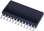
| 供应商器件封装 | 24-TSSOP |
| 信噪比 | 108 dB |
| 其它名称 | 598-1085-5 |
| 分辨率 | 24 bit |
| 分辨率(位) | 24 b |
| 功耗 | 135 mW |
| 包装 | 管件 |
| 商标 | Cirrus Logic |
| 商标名 | CS5351 |
| 安装类型 | 表面贴装 |
| 安装风格 | SMD/SMT |
| 封装 | Tube |
| 封装/外壳 | 24-TSSOP(0.173",4.40mm 宽) |
| 封装/箱体 | TSSOP-24 |
| 工作温度 | -10°C ~ 70°C |
| 工作电源电压 | 5 V |
| 工厂包装数量 | 62 |
| 数据接口 | 串行 |
| 最大工作温度 | + 70 C |
| 最小工作温度 | - 10 C |
| 标准包装 | 62 |
| 电压-电源 | 3.3V,5V |
| 电压源 | 模拟和数字 |
| 电源电压-最大 | 5.25 V |
| 电源电压-最小 | 4.75 V |
| 类型 | ADC, 音频 |
| 系列 | CS5351 |
| 转换器数量 | 2 |
| 转换速率 | 192 kS/s |
| 配用 | /product-detail/zh/CDB5351/598-1781-ND/2033738 |
| 采样率(每秒) | 192k |


- 商务部:美国ITC正式对集成电路等产品启动337调查
- 曝三星4nm工艺存在良率问题 高通将骁龙8 Gen1或转产台积电
- 太阳诱电将投资9.5亿元在常州建新厂生产MLCC 预计2023年完工
- 英特尔发布欧洲新工厂建设计划 深化IDM 2.0 战略
- 台积电先进制程称霸业界 有大客户加持明年业绩稳了
- 达到5530亿美元!SIA预计今年全球半导体销售额将创下新高
- 英特尔拟将自动驾驶子公司Mobileye上市 估值或超500亿美元
- 三星加码芯片和SET,合并消费电子和移动部门,撤换高东真等 CEO
- 三星电子宣布重大人事变动 还合并消费电子和移动部门
- 海关总署:前11个月进口集成电路产品价值2.52万亿元 增长14.8%


PDF Datasheet 数据手册内容提取
CS5351 108 dB, 192 kHz, Multi-bit Audio A/D Converter Features General Description (cid:141) Advanced Multi-bit Delta-Sigma Architecture The CS5351 is a complete analog-to-digital converter for digital audio systems. It performs sampling, analog- (cid:141) 24-bit Conversion to-digital conversion, and anti-alias filtering. The device generates 24-bit values for both left and right inputs in (cid:141) 108 dB Dynamic Range serial form at sample rates up to 192kHz per channel. The CS5351 uses a 5th-order, multi-bit, delta-sigma (cid:141) -98 dB THD+N modulator followed by digital filtering and decimation, which removes the need for an external anti-alias filter. (cid:141) System Sampling Rates up to 192 kHz The ADC uses a differential architecture which provides excellent noise rejection. (cid:141) 135 mW Power Consumption The CS5351 is ideal for audio systems requiring wide dynamic range, negligible distortion, and low noise. (cid:141) High-Pass Filter and DC Offset Calibration Such applications include A/V receivers, DVD-R, CD-R, digital mixing consoles, and effects processors. (cid:141) Supports Logic Levels Between 5 and 2.5 V ORDERING INFORMATION (cid:141) Single-Ended Analog Inputs CS5351-KSZ, Lead Free -10° to 70°C 24-pin SOIC CS5351-KZZ, Lead Free -10° to 70°C 24-pin TSSOP (cid:141) Overflow Detection CS5351-DZZ, Lead Free -40° to 85°C 24-pin TSSOP (cid:141) Pin Compatible with the CS5361 CDB5351 Evaluation Board VQ3VQ1VQ2 REFGND OVFL V SCLK LRCK SDOUT MCLK L RST FILT+ Voltage Reference Serial Output Interface I²S/LJ M/S + Digital High HPF AINL LP Filter ΔΣ Decimation Pass MDIV - Filter Filter S/H DAC + Digital High AINR LP Filter ΔΣ MODE0 Decimation Pass - Filter Filter MODE1 S/H DAC Copyright © Cirrus Logic, Inc. 2007 MAY '07 http://www.cirrus.com (All Rights Reserved) DS565F2
CS5351 TABLE OF CONTENTS 1. CHARACTERISTICS AND SPECIFICATIONS ......................................................................................4 SPECIFIED OPERATING CONDITIONS ..............................................................................................4 ABSOLUTE MAXIMUM RATINGS ........................................................................................................4 ANALOG CHARACTERISTICS (CS5351-KSZ/KZZ) .............................................................................5 ANALOG CHARACTERISTICS (CS5351-DZZ) ....................................................................................6 DIGITAL FILTER CHARACTERISTICS .................................................................................................7 DC ELECTRICAL CHARACTERISTICS ..............................................................................................10 DIGITAL CHARACTERISTICS ............................................................................................................10 THERMAL CHARACTERISTICS .........................................................................................................10 SWITCHING CHARACTERISTICS - SERIAL AUDIO PORT ..............................................................11 2. PIN DESCRIPTIONS ............................................................................................................................14 3. TYPICAL CONNECTION DIAGRAM ...................................................................................................15 4. APPLICATIONS ...................................................................................................................................16 4.1 Operational Mode/Sample Rate Range Select ..............................................................................16 4.2 System Clocking ............................................................................................................................16 4.2.1 Slave Mode ...........................................................................................................................16 4.2.2 Master Mode .........................................................................................................................17 4.3 Power-Up Sequence ......................................................................................................................17 4.4 Analog Connections .......................................................................................................................18 4.5 High-Pass Filter and DC Offset Calibration ...................................................................................18 4.6 Overflow Detection .........................................................................................................................19 4.6.1 OVFL Output Timing .............................................................................................................19 4.7 Grounding and Power Supply Decoupling .....................................................................................19 4.8 Synchronization of Multiple Devices ..............................................................................................19 5. PARAMETER DEFINITIONS ................................................................................................................20 6. PACKAGE DIMENSIONS .................................................................................................................21 7. REVISION HISTORY ............................................................................................................................23 2 DS565F2
CS5351 LIST OF FIGURES Figure 1. Single-Speed Mode Stopband Rejection .....................................................................................8 Figure 2. Single-Speed Mode Transition Band ...........................................................................................8 Figure 3. Single-Speed Mode Transition Band (Detail) ...............................................................................8 Figure 4. Single-Speed Mode Passband Ripple .........................................................................................8 Figure 5. Double-Speed Mode Stopband Rejection ....................................................................................8 Figure 6. Double-Speed Mode Transition Band ..........................................................................................8 Figure 7. Double-Speed Mode Transition Band (Detail) .............................................................................9 Figure 8. Double-Speed Mode Passband Ripple ........................................................................................9 Figure 9. Quad-Speed Mode Stopband Rejection ......................................................................................9 Figure 10. Quad-Speed Mode Transition Band ..........................................................................................9 Figure 11. Quad-Speed Mode Transition Band (Detail) ..............................................................................9 Figure 12. Quad-Speed Mode Passband Ripple ........................................................................................9 Figure 13. Master Mode, Left-Justified SAI ...............................................................................................12 Figure 14. Slave Mode, Left-Justified SAI .................................................................................................12 Figure 15. Master Mode, I²S SAI ...............................................................................................................12 Figure 16. Slave Mode, I²S SAI .................................................................................................................12 Figure 17. OVFL Output Timing ................................................................................................................12 Figure 18. Left-Justified Serial Audio Interface .........................................................................................13 Figure 19. I²S Serial Audio Interface .........................................................................................................13 Figure 20. OVFL Output Timing, I²S Format .............................................................................................13 Figure 21. OVFL Output Timing, Left-Justified Format .............................................................................13 Figure 22. Typical Connection Diagram ....................................................................................................15 Figure 23. CS5351 Master Mode Clocking ...............................................................................................17 Figure 24. CS5351 Recommended Analog Input Buffer ...........................................................................18 LIST OF TABLES Table 1. CS5351 Mode Control .................................................................................................................16 Table 2. CS5351 Slave Mode Clock Ratios ..............................................................................................16 Table 3. CS5351 Common Master Clock Frequencies .............................................................................17 DS565F2 3
CS5351 1. CHARACTERISTICS AND SPECIFICATIONS (All Min/Max characteristics and specifications are guaranteed over the Specified Operating Conditions. Typical performance characteristics and specifications are derived from measurements taken at typical supply voltages and T = 25°C.) A SPECIFIED OPERATING CONDITIONS (GND = 0V, all voltages with respect to 0V.) Parameter Symbol Min Typ Max Unit DC Power Supplies: Positive Analog VA 4.75 5.0 5.25 V Positive Digital VD 3.1 3.3 5.25 V Positive Logic VL 2.37 3.3 5.25 V Ambient Operating Temperature Commercial (-KSZ/-KZZ) T -10 - 70 °C AC Automotive (-DZZ) T -40 - 85 °C AI ABSOLUTE MAXIMUM RATINGS (GND = 0V, All voltages with respect to ground.) (Note 1) Parameter Symbol Min Max Units DC Power Supplies: Analog VA -0.3 +6.0 V Logic VL -0.3 +6.0 V Digital VD -0.3 +6.0 V Input Current (Note 2) I -10 +10 mA in Analog Input Voltage (Note 3) V GND-0.7 VA+0.7 V IN Digital Input Voltage (Note 3) V -0.7 VL+0.7 V IND Ambient Operating Temperature (Power Applied) T -50 +95 °C A Storage Temperature T -65 +150 °C stg Notes: 1. Operation beyond these limits may result in permanent damage to the device. Normal operation is not guaranteed at these extremes. 2. Any pin except supplies. Transient currents of up to ±100 mA on the analog input pins will not cause SCR latch-up. 3. The maximum over/under voltage is limited by the input current. 4 DS565F2
CS5351 ANALOG CHARACTERISTICS (CS5351-KSZ/KZZ) (Test conditions (unless otherwise specified): Input test signal is a 1kHz sine wave; measurement bandwidth is 10Hz to 20kHz.) Parameter Symbol Min Typ Max Unit Single-Speed Mode Fs = 48kHz Dynamic Range A-weighted 102 108 - dB unweighted 99 105 - dB Total Harmonic Distortion + Noise (Note 4) THD+N -1dB - -98 -92 dB -20dB - -84 - dB -60dB - -44 - dB Double-Speed Mode Fs = 96kHz Dynamic Range A-weighted 102 108 - dB unweighted 99 105 - dB 40kHz bandwidth unweighted - 102 - dB Total Harmonic Distortion + Noise (Note 4) THD+N -1dB - -98 -92 dB -20dB - -84 - dB -60dB - -44 - dB 40kHz bandwidth -1dB - -95 - dB Quad-Speed Mode Fs = 192kHz Dynamic Range A-weighted 102 108 - dB unweighted 99 105 - dB 40kHz bandwidth unweighted - 102 - dB Total Harmonic Distortion + Noise (Note 4) THD+N -1dB - -98 -92 dB -20dB - -84 - dB -60dB - -44 - dB 40kHz bandwidth -1dB - -95 - dB Dynamic Performance for All Modes Interchannel Isolation - 95 - dB DC Accuracy Interchannel Gain Mismatch - 0.1 - dB Gain Error -2 - 2 % Gain Drift -100 - 100 ppm/°C Offset Error HPF enabled - - 0 LSB HPF disabled - - 100 LSB Analog Input Characteristics Full-scale Input Voltage 0.55*VA 0.56*VA .57*VA Vpp Input Impedance 7.5 - - kΩ Common Mode Rejection Ratio CMRR - 82 - dB Notes: 4. Referred to the typical full-scale input voltage. DS565F2 5
CS5351 ANALOG CHARACTERISTICS (CS5351-DZZ) (Test conditions (unless otherwise specified): Input test signal is a 1kHz sine wave; measurement bandwidth is 10Hz to 20kHz.) Parameter Symbol Min Typ Max Unit Single-Speed Mode Fs = 48kHz Dynamic Range A-weighted 100 108 - dB unweighted 97 105 - dB Total Harmonic Distortion + Noise (Note 4) THD+N -1dB - -98 -90 dB -20dB - -84 - dB -60dB - -44 - dB Double-Speed Mode Fs = 96kHz Dynamic Range A-weighted 100 108 - dB unweighted 97 105 - dB 40kHz bandwidth unweighted - 102 - dB Total Harmonic Distortion + Noise (Note 4) THD+N -1dB - -98 -90 dB -20dB - -84 - dB -60dB - -44 - dB 40kHz bandwidth -1dB - -95 - dB Quad-Speed Mode Fs = 192kHz Dynamic Range A-weighted 100 108 - dB unweighted 97 105 - dB 40kHz bandwidth unweighted - 102 - dB Total Harmonic Distortion + Noise (Note 4) THD+N -1dB - -98 -90 dB -20dB - -84 - dB -60dB - -44 - dB 40kHz bandwidth -1dB - -95 - dB Dynamic Performance for All Modes Interchannel Isolation - 95 - dB DC Accuracy Interchannel Gain Mismatch - 0.1 - dB Gain Error -5 - 5 % Gain Drift -100 - 100 ppm/°C Offset Error HPF enabled - - 0 LSB HPF disabled - - 100 LSB Analog Input Characteristics Full-scale Input Voltage 0.53*VA 0.56*VA 0.59*VA Vpp Input Impedance 7.5 - - kΩ Common Mode Rejection Ratio CMRR - 82 - dB 6 DS565F2
CS5351 DIGITAL FILTER CHARACTERISTICS Parameter Symbol Min Typ Max Unit Single-Speed Mode (2kHz to 51kHz sample rates) Passband (-0.1dB) (Note 5) 0 - 0.47 Fs Passband Ripple -0.1 - 0.035 dB Stopband (Note 5) 0.58 - - Fs Stopband Attenuation -95 - - dB Total Group Delay (Fs = Output Sample Rate) t - 12/Fs - s gd Interchannel Phase Deviation - 0.0001 - Deg Double-Speed Mode (50kHz to 102kHz sample rates) Passband (-0.1dB) (Note 5) 0 - 0.45 Fs Passband Ripple -0.1 - 0.035 dB Stopband (Note 5) 0.68 - - Fs Stopband Attenuation -92 - - dB Total Group Delay (Fs = Output Sample Rate) t - 9/Fs - s gd Interchannel Phase Deviation - 0.0001 - Deg Quad-Speed Mode (100kHz to 204kHz sample rates) Passband (-0.1dB) (Note 5) 0 - 0.24 Fs Passband Ripple -0.1 - 0.035 dB Stopband (Note 5) 0.78 - - Fs Stopband Attenuation -92 - - dB Total Group Delay (Fs = Output Sample Rate) t - 5/Fs - s gd Interchannel Phase Deviation - 0.0001 - Deg High Pass Filter Characteristics Frequency Response -3.0dB - 1 - Hz -0.13dB (Note 6) 20 - Hz Phase Deviation @ 20Hz (Note 6) - 10 - Deg Passband Ripple - - 0 dB Filter Settling Time 105/Fs s Notes: 5. The filter frequency response scales precisely with Fs. 6. Response shown is for Fs equal to 48kHz. Filter characteristics scale with Fs. DS565F2 7
CS5351 0 0 -10 -10 -20 -20 -30 -30 -40 -40 -50 -50 Amplitude (dB) ---876000 Amplitude (dB) ---876000 -90 -90 -100 -100 -110 -110 -120 -120 -130 -130 -1400.0 0.1 0.2 0.3 0.4 0.5 0.6 0.7 0.8 0.9 1.0 -1400.40 0.42 0.44 0.46 0.48 0.50 0.52 0.54 0.56 0.58 0.60 Frequency (normalized to Fs) Frequency (normalized to Fs) Figure 1. Single-Speed Mode Stopband Rejection Figure 2. Single-Speed Mode Transition Band 0 0.10 -1 0.08 -2 0.05 -3 0.03 Amplitude (dB) ---654 Amplitude (dB)-00..0030 -7 -0.05 -8 -0.08 -9 -100.45 0.46 0.47 0.48 0.49 0.50 0.51 0.52 0.53 0.54 0.55 -0.100.00 0.05 0.10 0.15 0.20 0.25 0.30 0.35 0.40 0.45 0.50 Frequency (normalized to Fs) Frequency (normalized to Fs) Figure 3. Single-Speed Mode Transition Band (Detail) Figure 4. Single-Speed Mode Passband Ripple 0 0 -10 -10 -20 -20 -30 -30 -40 -40 -50 -50 Amplitude (dB) ---876000 Amplitude (dB) ---876000 -90 -90 -100 -100 -110 -110 -120 -120 -130 -130 -140 -140 0.0 0.1 0.2 0.3 0.4 0.5 0.6 0.7 0.8 0.9 1.0 0.40 0.43 0.45 0.48 0.50 0.53 0.55 0.58 0.60 0.63 0.65 0.68 0.70 Frequency (normalized to Fs) Frequency (normalized to Fs) Figure 5. Double-Speed Mode Stopband Rejection Figure 6. Double-Speed Mode Transition Band 8 DS565F2
CS5351 0 0.10 -1 0.08 -2 0.05 -3 0.03 mplitude (dB) --54 mplitude (dB) 0.00 A -6 A-0.03 -7 -0.05 -8 -9 -0.08 -10 -0.10 0.40 0.43 0.45 0.48 0.50 0.53 0.55 0.00 0.05 0.10 0.15 0.20 0.25 0.30 0.35 0.40 0.45 0.50 Frequency (normalized to Fs) Frequency (normalized to Fs) Figure 7. Double-Speed Mode Transition Band (Detail) Figure 8. Double-Speed Mode Passband Ripple Amplitude (dB) Amplitude (dB) Frequency (normalized to Fs) Frequency (normalized to Fs) Figure 9. Quad-Speed Mode Stopband Rejection Figure 10. Quad-Speed Mode Transition Band Amplitude (dB) Amplitude (dB) Frequency (normalized to Fs) Frequency (normalized to Fs) Figure 11. Quad-Speed Mode Transition Band (Detail) Figure 12. Quad-Speed Mode Passband Ripple DS565F2 9
CS5351 DC ELECTRICAL CHARACTERISTICS (GND = 0V, all voltages with respect to ground. MCLK=12.288MHz; Master Mode) Parameter Symbol Min Typ Max Unit Power Supply Current VA = 5V I - 17.5 21.5 mA A (Normal Operation) VL,VD = 5V I - 22 27.5 mA D VL,VD = 3.3V I - 14.5 17 mA D Power Supply Current VA = 5V I - 100 - μA A (Power-Down Mode) (Note 7) VL,VD = 5V I - 100 - μA D Power Consumption (Normal Operation) VA, VD, VL = 5V - - 198 243 mW VA = 5V, VL, VD = 3.3V - - 135 161 mW (Power-Down Mode) - - 1 - mW Power Supply Rejection Ratio (1 kHz) (Note 8) PSRR - 65 - dB V Nominal Voltage - 2.5 - V Q Output Impedance - 25 - kΩ Maximum allowable DC current source/sink - 0.01 - mA Filt+ Nominal Voltage - 5 - V Output Impedance - 15 - kΩ Maximum allowable DC current source/sink - 0.01 - mA Notes: 7. Power Down Mode is defined as RST = Low with all clocks and data lines held static. 8. Valid with the recommended capacitor values on FILT+ and VQ as shown in the Typical Connection Diagram. DIGITAL CHARACTERISTICS Parameter Symbol Min Typ Max Units High-Level Input Voltage (% of VL) V 70% - - V IH Low-Level Input Voltage (% of VL) V - - 30% V IL High-Level Output Voltage at I = 100μA (% of VL) V 70% - - V o OH Low-Level Output Voltage at I = 100μA (% of VL) V - - 15% V o OL OVFL Current Sink I - - 4.0 mA ovfl Input Leakage Current (all pins except SCLK and LRCK) I -10 - 10 μA in Input Leakage Current (SCLK and LRCK) I -25 - 25 μA in THERMAL CHARACTERISTICS Parameter Symbol Min Typ Max Unit Allowable Junction Temperature - - 135 °C Junction to Ambient Thermal Impedance θ (Multi-layer PCB) TSSOP θJA-TM - 70 - °C/W (Multi-layer PCB) SOIC θJA-SM - 60 - °C/W (Single-layer PCB) TSSOP θJA-TS - 105 - °C/W (Single-layer PCB) SOIC JA-SS - 80 - °C/W 10 DS565F2
CS5351 SWITCHING CHARACTERISTICS - SERIAL AUDIO PORT (Logic "0" = GND = 0V; Logic "1" = VL, C = 20pF) L Parameter Symbol Min Typ Max Unit Output Sample Rate Single-Speed Mode Fs 2 - 51 kHz Double-Speed Mode Fs 50 - 102 kHz Quad-Speed Mode Fs 100 - 204 kHz OVFL to LRCK edge setup time t 16/f - - s setup sclk OVFL to LRCK edge hold time t 1/f - - s hold sclk OVFL time-out on overrange condition Fs = 44.1, 88.2, 176.4kHz - 740 - ms Fs = 48, 96, 192kHz - 680 - ms MCLK Specifications MCLK Period t 38 - 1953 ns clkw MCLK Pulse Duty Cycle 40 50 60 % Master Mode SCLK falling to LRCK t -20 - 20 ns mslr SCLK falling to SDOUT valid t 0 - 32 ns sdo SCLK Duty Cycle - 50 - % Slave Mode Single-Speed Output Sample Rate Fs 2 - 51 kHz LRCK Duty Cycle 40 50 60 % SCLK Period t 153 - - ns sclkw SCLK Duty Cycle 45 50 55 % SCLK falling to SDOUT valid t - - 32 ns dss SCLK falling to LRCK edge t -20 - 20 ns slrd Double-Speed Output Sample Rate Fs 50 - 102 kHz LRCK Duty Cycle 40 50 60 % SCLK Period t 153 - - ns sclkw SCLK Duty Cycle 45 50 55 % SCLK falling to SDOUT valid t - - 32 ns dss SCLK falling to LRCK edge t -20 - 20 ns slrd Quad-Speed Output Sample Rate Fs 100 - 204 kHz LRCK Duty Cycle 40 50 60 % SCLK Period t 77 - - ns sclkw SCLK Duty Cycle 45 50 55 % SCLK falling to SDOUT valid t - - 32 ns dss SCLK falling to LRCK edge t -8 - 3 ns slrd DS565F2 11
CS5351 SCLK output CLKinput tmslr tslrd tsclkw LRCK output LRCK input tsdo t dss SDOUT MSB MSB-1 SDOUT MSB MSB-1 MSB-2 Figure 13. Master Mode, Left-Justified SAI Figure 14. Slave Mode, Left-Justified SAI SCLKinput SCLKinput tslrd tsclkw tslrd tsclkw LRCK input LRCK input t t dss dss MSB MSB-1 MSB MSB-1 SDOUT SDOUT Figure 15. Master Mode, I²S SAI Figure 16. Slave Mode, I²S SAI LRCK tsetup thold OVFL Figure 17. OVFL Output Timing 12 DS565F2
CS5351 LRCK LeftChannel RightChannel SCLK SDATA 2322 9 8 7 6 5 4 3 2 1 0 2322 9 8 7 6 5 4 3 2 1 0 2322 Figure 18. Left-Justified Serial Audio Interface LRCK LeftChannel RightChannel SCLK SDATA 2322 9 8 7 6 5 4 3 2 1 0 2322 9 8 7 6 5 4 3 2 1 0 2322 Figure 19. I²S Serial Audio Interface LRCK SCLK OVFL OVFL_R OVFL_L OVFL_R Figure 20. OVFL Output Timing, I²S Format LRCK SCLK OVFL OVFL_R OVFL_L OVFL_R Figure 21. OVFL Output Timing, Left-Justified Format DS565F2 13
CS5351 2. PIN DESCRIPTIONS RST 1 24 FILT+ M/S 2 23 REFGND LRCK 3 22 VQ3 SCLK 4 21 AINR MCLK 5 20 VQ2 VD 6 19 VA GND 7 18 GND VL 8 17 VQ1 SDOUT 9 16 AINL MDIV 10 15 OVFL HPF 11 14 M1 I²S/LJ 12 13 M0 Pin Name # Pin Description RST 1 Reset (Input) - The device enters a low power mode when low. M/S 2 Master/Slave Mode (Input) - Selects operation as either clock master or slave. 3 Left Right Clock (Input/Output) - Determines which channel, Left or Right, is currently active on the LRCK serial audio data line. SCLK 4 Serial Clock (Input/Output) - Serial clock for the serial audio interface. MCLK 5 Master Clock (Input) - Clock source for the delta-sigma modulator and digital filters. VD 6 Digital Power (Input) - Positive power supply for the digital section. 7 GND Ground (Input) - Ground reference. Must be connected to analog ground. 18 VL 8 Logic Power (Input) - Positive power for the digital input/output. SDOUT 9 Serial Audio Data Output (Output) - Output for two’s complement serial audio data. MDIV 10 MCLK Divider (Input) - Enables a master clock divide by two function. HPF 11 High Pass Filter Enable (Input) - Enables the Digital High-Pass Filter. I²S/LJ 12 Serial Audio Interface Format Select (Input) -Selects either the Left-Justified or I²S format for the SAI. M0 13 Mode Selection (Input) - Determines the operational mode of the device. M1 14 OVFL 15 Overflow (Output, open drain) - Detects an overflow condition on both left and right channels. AINL 16 Analog Inputs (Input) - The full-scale analog input level is specified in the Analog Characteristics speci- AINR 21 fication table. VQ1 17 VQ2 20 Quiescent Voltage (Output) - Filter connection for the internal quiescent reference voltage. VQ3 22 VA 19 Analog Power (Input) - Positive power supply for the analog section. REF_GND 23 Reference Ground (Input) - Ground reference for the internal sampling circuits. FILT+ 24 Positive Voltage Reference (Output) - Positive reference voltage for the internal sampling circuits. 14 DS565F2
CS5351 3. TYPICAL CONNECTION DIAGRAM +5 V to 3.3 V + + +5Vto2.5V 1 μF 0.01μF 0.01μF 1 μF * +5V + 0.01 μF 1 μF 0.01μF 5.1 Ω VA VD VL FILT+ + VL 47μF 0.01μF REFGND 10 kΩ OVFL RST I2S/LJ Power Down M/S AINL and Mode HPF Analog VQ1 CS5351 M0 Settings Input M1 Buffer VQ3 A/DCONVERTER MDIV (Figure 24) VQ2 AINR AudioData SDOUT Processor LRCK SCLK TimingLogic andClock MCLK * Resistor may only be used if VD is derived from VA. If used, do not drive any other GND GND logic from VD Figure 22. Typical Connection Diagram DS565F2 15
CS5351 4. APPLICATIONS 4.1 Operational Mode/Sample Rate Range Select The output sample rate, Fs, can be adjusted from 2kHz to 204kHz. The CS5351 must be set to the proper speed mode via the mode pins, M1 and M0. Refer to Table1. M1 (Pin 14) M0 (Pin 13) MODE Output Sample Rate (Fs) 0 0 Single-Speed Mode 2kHz - 51kHz 0 1 Double-Speed Mode 50kHz - 102kHz 1 0 Quad-Speed Mode 100kHz - 204kHz 1 1 Reserved Table 1. CS5351 Mode Control 4.2 System Clocking The device supports operation in either Master Mode, where the left/right and serial clocks are synchronous- ly generated on-chip, or Slave Mode, which requires external generation of the left/right and serial clocks. The device also includes a master clock divider in Master Mode where the master clock will be internally divided prior to any other internal circuitry when MDIV is enabled, set to logic 1. In Slave Mode, the MDIV pin needs to be disabled, set to logic 0. 4.2.1 Slave Mode LRCK and SCLK operate as inputs in Slave Mode. The left/right clock must be synchronously derived from the master clock and be equal to Fs. It is also recommended that the serial clock be synchronously derived from the master clock and be equal to 64x Fs to maximize system performance. Refer to Table2 for required clock ratios. Single-Speed Mode Double-Speed Mode Quad-Speed Mode Fs = 2kHz to 51kHz Fs = 50kHz to 102kHz Fs = 100kHz to 204kHz MCLK/LRCK Ratio 256x, 512x 128x, 256x 128x SCLK/LRCK Ratio 32x, 64x, 128x 32x, 64x 32x, 64x Table 2. CS5351 Slave Mode Clock Ratios 16 DS565F2
CS5351 4.2.2 Master Mode In Master Mode, LRCK and SCLK operate as outputs. The left/right and serial clocks are internally derived from the master clock with the left/right clock equal to Fs and the serial clock equal to 64x Fs, as shown in Figure23. Refer to Table3 for common master clock frequencies. Single ÷ 256 00 Speed ÷ 128 Double 01 LRCK Output Speed (Equal to Fs) Quad ÷ 64 10 Speed ÷ 1 0 MCLK M1 M0 ÷ 2 1 Single ÷ 4 00 Speed MDIV ÷ 2 Double 01 SCLK Output Speed Quad ÷ 1 10 Speed Figure 23. CS5351 Master Mode Clocking MDIV = 0 MDIV = 1 SAMPLE RATE (kHz) MCLK (MHz) MCLK (MHz) 32 8.192 16.384 44.1 11.2896 22.5792 48 12.288 24.576 64 8.192 16.384 88.2 11.2896 22.5792 96 12.288 24.576 176.4 11.2896 22.5792 192 12.288 24.576 Table 3. CS5351 Common Master Clock Frequencies 4.3 Power-Up Sequence Reliable power-up can be accomplished by keeping the device in reset until the power supplies, clocks and configuration pins are stable. It is also recommended that reset be enabled if the analog or digital supplies drop below the minimum specified operating voltages to prevent power glitch related issues. The internal reference voltage must be stable for the device to produce valid data. Therefore, there is a de- lay between the release of reset and the generation of valid output due to the finite output impedance of FILT+ and the presence of the external capacitance. DS565F2 17
CS5351 4.4 Analog Connections The analog modulator samples the input at 6.144MHz. The digital filter will reject signals within the stop- × band of the filter. However, there is no rejection for input signals which are (n 6.144MHz) the digital pass- band frequency, where n=0,1,2,...Refer to Figure24 which shows the suggested filter that will attenuate any noise energy at 6.144MHz, in addition to providing the optimum source impedance for the modulators. The use of capacitors which have a large voltage coefficient (such as general purpose ceramics) must be avoid- ed since these can degrade signal linearity. 634Ω 470 pF CS5351 C0G - 91Ω 1μF AINL + 2700 pF C0G 100 kΩ 100 kΩ VQ1 - + VQ3 1μF 0.01μF 100 kΩ VQ2 2700 pF + C0G 1μF AINR 100 kΩ - 91Ω 470 pF C0G 634Ω Figure 24. CS5351 Recommended Analog Input Buffer 4.5 High-Pass Filter and DC Offset Calibration The operational amplifiers in the input circuitry driving the CS5351 may generate a small DC offset into the A/D converter. The CS5351 includes a high pass filter after the decimator to remove any DC offset which could result in recording a DC level, possibly yielding "clicks" when switching between devices in a multi- channel system. The high pass filter continuously subtracts a measure of the DC offset from the output of the decimation filter. If the HPF pin is taken high during normal operation, the current value of the DC offset register is frozen and this DC offset will continue to be subtracted from the conversion result. This feature makes it possible to perform a system DC offset calibration by: Running the CS5351 with the high pass filter enabled until the filter settles. See the Digital Filter Character- istics for filter settling time. Disabling the high pass filter and freezing the stored DC offset. A system calibration performed in this way will eliminate offsets anywhere in the signal path between the calibration point and the CS5351. 18 DS565F2
CS5351 4.6 Overflow Detection The CS5351 includes overflow detection on both the left and right channels. This time multiplexed informa- tion is presented as open drain, active low on pin 15, OVFL. The OVFL_L and OVFL_R data will go to a logical low as soon as an overrange condition in either channel is detected. The data will remain low as specified in the Switching Characteristics - Serial Audio Port section. This ensures sufficient time to detect an overrange condition regardless of the speed mode. After the timeout, the OVFL_L and OVFL_R data will return to a logical high if there has not been any other overrange condition detected. Please note that an overrange condition on either channel will restart the timeout period for both channels. 4.6.1 OVFL Output Timing In Left-Justified format, the OVFL pin is updated one SCLK period after an LRCK transition. In I²S format, the OVFL pin is updated two SCLK periods after an LRCK transition. Refer to Figures23 and 24. In both cases the OVFL data can be easily demultiplexed by using the LRCK to latch the data. In left-justified for- mat, the rising edge of LRCK would latch the right channel overflow status, and the falling edge of LRCK would latch the left channel overflow status. In I²S format, the falling edge of LRCK would latch the right channel overflow status and the rising edge of LRCK would latch the left channel overflow status. 4.7 Grounding and Power Supply Decoupling As with any high-resolution converter, the CS5351 requires careful attention to power supply and grounding arrangements if its potential performance is to be realized. Figure22 shows the recommended power ar- rangements, with VA and VL connected to clean supplies. VD, which powers the digital filter, may be run from the system logic supply or may be powered from the analog supply via a resistor. In this case, no ad- ditional devices should be powered from VD. Decoupling capacitors should be as near to the ADC as pos- sible, with the low value ceramic capacitor being the nearest. All signals, especially clocks, should be kept away from the FILT+ and VQ pins in order to avoid unwanted coupling into the modulators. The FILT+ and VQ decoupling capacitors, particularly the 0.01µF, must be positioned to minimize the electrical path from FILT+ and REFGND. The CDB5351 evaluation board demonstrates the optimum layout and power supply arrangements. To minimize digital noise, connect the ADC digital outputs only to CMOS inputs. 4.8 Synchronization of Multiple Devices In systems where multiple ADCs are required, care must be taken to achieve simultaneous sampling. To ensure synchronous sampling, the MCLK and LRCK must be the same for all of the CS5351’s in the system. If only one master clock source is needed, one solution is to place one CS5351 in Master Mode, and slave all of the other CS5351’s to the one master. If multiple master clock sources are needed, a possible solution would be to supply all clocks from the same external source and time the CS5351 reset with the inactive edge of MCLK. This will ensure that all converters begin sampling on the same clock edge. DS565F2 19
CS5351 5. PARAMETER DEFINITIONS Dynamic Range The ratio of the rms value of the signal to the rms sum of all other spectral components over the specified bandwidth. Dynamic Range is a signal-to-noise ratio measurement over the specified bandwidth made with a -60dBFS signal. 60dB is added to resulting measurement to refer the measurement to full-scale. This technique ensures that the distortion components are below the noise level and do not affect the measurement. This measurement technique has been accepted by the Audio Engineering Society, AES17-1991, and the Electronic Industries Association of Japan, EIAJ CP-307. Expressed in decibels. Total Harmonic Distortion + Noise The ratio of the rms value of the signal to the rms sum of all other spectral components over the specified bandwidth (typically 10Hz to 20kHz), including distortion components. Expressed in decibels. Measured at -1 and -20dBFS as suggested in AES17-1991 Annex A. Frequency Response A measure of the amplitude response variation from 10Hz to 20kHz relative to the amplitude response at 1kHz. Units in decibels. Interchannel Isolation A measure of crosstalk between the left and right channels. Measured for each channel at the converter's output with no signal to the input under test and a full-scale signal applied to the other channel. Units in decibels. Interchannel Gain Mismatch The gain difference between left and right channels. Units in decibels. Gain Error The deviation from the nominal full-scale analog output for a full-scale digital input. Gain Drift The change in gain value with temperature. Units in ppm/°C. Offset Error The deviation of the mid-scale transition (111...111 to 000...000) from the ideal. Units in mV. 20 DS565F2
CS5351 6. PACKAGE DIMENSIONS 24L SOIC (300 MIL BODY) PACKAGE DRAWING E H 1 b c ∝ D L SEATING PLANE A e A1 INCHES MILLIMETERS DIM MIN MAX MIN MAX A 0.093 0.104 2.35 2.65 A1 0.004 0.012 0.10 0.30 B 0.013 0.020 0.33 0.51 C 0.009 0.013 0.23 0.32 D 0.598 0.614 15.20 15.60 E 0.291 0.299 7.40 7.60 e 0.040 0.060 1.02 1.52 H 0.394 0.419 10.00 10.65 L 0.016 0.050 0.40 1.27 ∝ 0° 8° 0° 8° DS565F2 21
CS5351 24L TSSOP (4.4 mm BODY) PACKAGE DRAWING N D E11 E A2 A ∝ A1 e b2 L END VIEW SEATING PLANE SIDE VIEW 1 2 3 TOP VIEW INCHES MILLIMETERS NOTE DIM MIN NOM MAX MIN NOM MAX A -- -- 0.043 -- -- 1.10 A1 0.002 0.004 0.006 0.05 -- 0.15 A2 0.03346 0.0354 0.037 0.85 0.90 0.95 b 0.00748 0.0096 0.012 0.19 0.245 0.30 2,3 D 0.303 0.307 0.311 7.70 7.80 7.90 1 E 0.248 0.2519 0.256 6.30 6.40 6.50 E1 0.169 0.1732 0.177 4.30 4.40 4.50 1 e -- 0.026 BSC -- -- 0.65 BSC -- L 0.020 0.024 0.028 0.50 0.60 0.70 µ 0° 4° 8° 0° 4° 8° JEDEC #: MO-153 Controlling Dimension is Millimeters. Notes: 1. “D” and “E1” are reference datums and do not included mold flash or protrusions, but do include mold mismatch and are measured at the parting line, mold flash or protrusions shall not exceed 0.20mm per side. 2. Dimension “b” does not include dambar protrusion/intrusion. Allowable dambar protrusion shall be 0.13mm total in excess of “b” dimension at maximum material condition. Dambar intrusion shall not re- duce dimension “b” by more than 0.07mm at least material condition. 3. These dimensions apply to the flat section of the lead between 0.10 and 0.25mm from lead tips. 22 DS565F2
CS5351 7. REVISION HISTORY Release Changes PP2 Preliminary datasheet. F1 Improve Gain Error specification under Analog Characteristics. Specify Full-scale Input Voltage in terms of VA under Analog Characteristics. Update Differential Input Impedance under Analog Characteristics. Increase maximum Power-Supply Current, I , under DC Electrical Characteristics. A Reduce maximum Power Consumption under DC Electrical Characteristics. Update FILT+ Output Impedance specification under DC Electrical Characteristics. Extend maximum Fs in Single-Speed Mode to 51 kHz. Extend maximum Fs in Double-Speed Mode to 102 kHz. Extend maximum Fs in Quad-Speed Mode to 204 kHz. Decrease maximum SCLK falling to LRCK edge specification in Quad-Speed Mode. Replace minimum MCLK high/low timing specifications with duty cycle specification. Replace minimum SCLK high/low timing specifications with duty cycle specification. Replace recommended analog input buffer with new input buffer topology. F2 Updated ordering information. Contacting Cirrus Logic Support For all product questions and inquiries, contact a Cirrus Logic Sales Representative. To find the one nearest you, go to www.cirrus.com. IMPORTANT NOTICE Cirrus Logic, Inc. and its subsidiaries ("Cirrus") believe that the information contained in this document is accurate and reliable. However, the information is subject to change without notice and is provided "AS IS" without warranty of any kind (express or implied). Customers are advised to obtain the latest version of relevant information to verify, before placing orders, that information being relied on is current and complete. All products are sold subject to the terms and conditions of sale supplied at the time of order acknowledgment, including those pertaining to warranty, indemnification, and limitation of liability. No responsibility is assumed by Cirrus for the use of this information, including use of this information as the basis for manufacture or sale of any items, or for infringement of patents or other rights of third parties. This document is the property of Cirrus and by furnishing this information, Cirrus grants no license, express or implied under any patents, mask work rights, copyrights, trademarks, trade secrets or other intellectual property rights. Cirrus owns the copyrights associated with the information contained herein and gives con- sent for copies to be made of the information only for use within your organization with respect to Cirrus integrated circuits or other products of Cirrus. This consent does not extend to other copying such as copying for general distribution, advertising or promotional purposes, or for creating any work for resale. CERTAIN APPLICATIONS USING SEMICONDUCTOR PRODUCTS MAY INVOLVE POTENTIAL RISKS OF DEATH, PERSONAL INJURY, OR SEVERE PROP- ERTY OR ENVIRONMENTAL DAMAGE (“CRITICAL APPLICATIONS”). CIRRUS PRODUCTS ARE NOT DESIGNED, AUTHORIZED OR WARRANTED FOR USE IN AIRCRAFT SYSTEMS, MILITARY APPLICATIONS, PRODUCTS SURGICALLY IMPLANTED INTO THE BODY, AUTOMOTIVE SAFETY OR SECURITY DE- VICES, LIFE SUPPORT PRODUCTS OR OTHER CRITICAL APPLICATIONS. INCLUSION OF CIRRUS PRODUCTS IN SUCH APPLICATIONS IS UNDER- STOOD TO BE FULLY AT THE CUSTOMER’S RISK AND CIRRUS DISCLAIMS AND MAKES NO WARRANTY, EXPRESS, STATUTORY OR IMPLIED, INCLUDING THE IMPLIED WARRANTIES OF MERCHANTABILITY AND FITNESS FOR PARTICULAR PURPOSE, WITH REGARD TO ANY CIRRUS PRODUCT THAT IS USED IN SUCH A MANNER. IF THE CUSTOMER OR CUSTOMER’S CUSTOMER USES OR PERMITS THE USE OF CIRRUS PRODUCTS IN CRITICAL APPLICATIONS, CUSTOMER AGREES, BY SUCH USE, TO FULLY INDEMNIFY CIRRUS, ITS OFFICERS, DIRECTORS, EMPLOYEES, DISTRIBUTORS AND OTHER AGENTS FROM ANY AND ALL LIABILITY, INCLUDING ATTORNEYS’ FEES AND COSTS, THAT MAY RESULT FROM OR ARISE IN CONNECTION WITH THESE USES. Cirrus Logic, Cirrus, and the Cirrus Logic logo designs are trademarks of Cirrus Logic, Inc. All other brand and product names in this document may be trademarks or service marks of their respective owners. DS565F2 23
Mouser Electronics Authorized Distributor Click to View Pricing, Inventory, Delivery & Lifecycle Information: C irrus Logic: CDB5351 CS5351-DZZ CS5351-DZZR CS5351-KSZ CS5351-KSZR CS5351-KZZ CS5351-KZZR