
 Datasheet下载
- 型号: CY7C1041CV33-8ZSXI
- 制造商: Cypress Semiconductor
- 库位|库存: xxxx|xxxx
- 要求:
| 数量阶梯 | 香港交货 | 国内含税 |
| +xxxx | $xxxx | ¥xxxx |
查看当月历史价格
查看今年历史价格
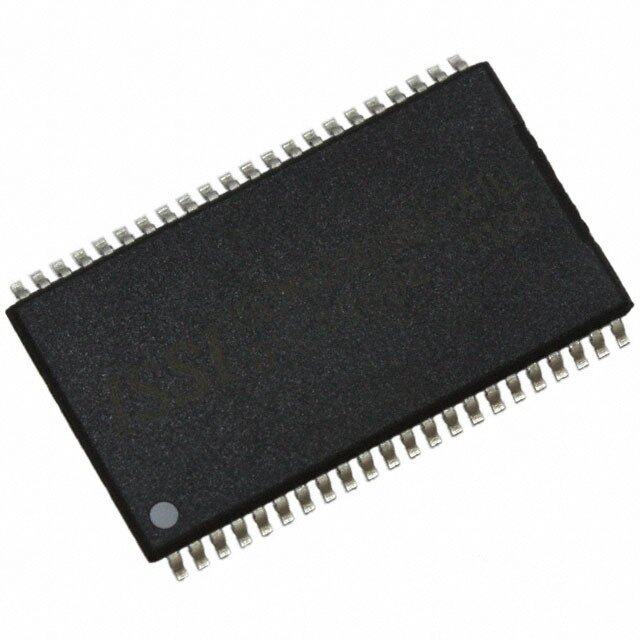
CY7C1041CV33-8ZSXI产品简介:
ICGOO电子元器件商城为您提供CY7C1041CV33-8ZSXI由Cypress Semiconductor设计生产,在icgoo商城现货销售,并且可以通过原厂、代理商等渠道进行代购。 CY7C1041CV33-8ZSXI价格参考。Cypress SemiconductorCY7C1041CV33-8ZSXI封装/规格:存储器, SRAM - 异步 存储器 IC 4Mb (256K x 16) 并联 8ns 44-TSOP II。您可以下载CY7C1041CV33-8ZSXI参考资料、Datasheet数据手册功能说明书,资料中有CY7C1041CV33-8ZSXI 详细功能的应用电路图电压和使用方法及教程。
CY7C1041CV33-8ZSXI 是赛普拉斯半导体公司(Cypress Semiconductor Corp)生产的一款静态随机存取存储器(SRAM),其容量为256K x 4位,工作电压为3.3V,访问速度为8ns,采用SOJ封装,工业级温度范围。

该器件主要应用于对数据读写速度和稳定性要求较高的场景,常见应用包括:

1. 网络与通信设备:如路由器、交换机等,用于高速缓存数据包或临时存储路由表信息。
2. 工业控制系统:用于PLC、工业计算机或自动化设备中,作为快速存储中间运算结果或配置数据的存储单元。
3. 测试测量仪器:例如示波器、逻辑分析仪等,用于高速数据采集与临时存储。
4. 汽车电子系统:在车载控制模块(如发动机控制、ADAS系统)中用于实时数据处理和缓存。
5. 医疗设备:如成像设备、监护仪等,支持高速数据处理与临时存储以提高响应速度。

该SRAM因其高速访问能力和宽温特性,适合于需要可靠性和高性能的嵌入式系统和实时控制系统中使用。
| 参数 | 数值 |
| 产品目录 | 集成电路 (IC)半导体 |
| 描述 | IC SRAM 4MBIT 8NS 44TSOP静态随机存取存储器 4Mb 8ns 256K x 16 Fast Async 静态随机存取存储器 |
| 产品分类 | |
| 品牌 | Cypress Semiconductor Corp |
| 产品手册 | |
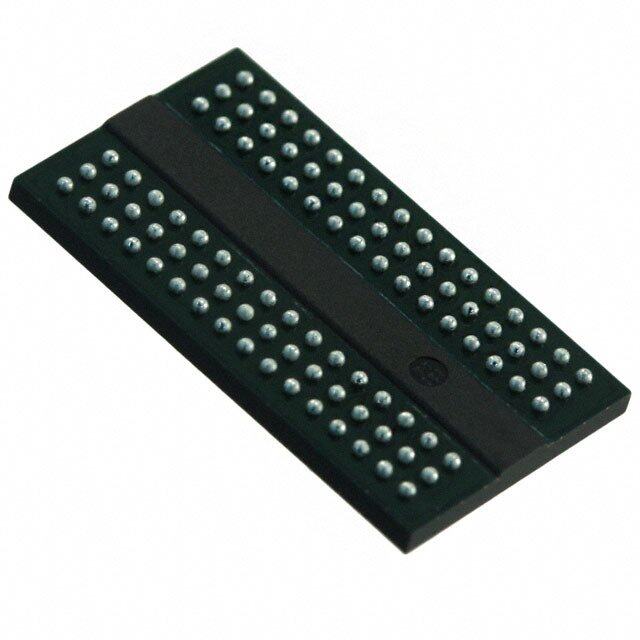
| 产品图片 |
|
| rohs | 符合RoHS无铅 / 符合限制有害物质指令(RoHS)规范要求 |
| 产品系列 | 内存,静态随机存取存储器,Cypress Semiconductor CY7C1041CV33-8ZSXI- |
| 数据手册 | http://www.cypress.com/?docID=48464 |
| 产品型号 | CY7C1041CV33-8ZSXI |
| PCN组件/产地 | http://www.cypress.com/?docID=48115http://www.cypress.com/?docID=49741 |
| 产品种类 | 静态随机存取存储器 |
| 供应商器件封装 | 44-TSOP II |
| 其它名称 | 428-3284 |
| 包装 | 托盘 |
| 商标 | Cypress Semiconductor |
| 存储器类型 | SRAM - 异步 |
| 存储容量 | 4M (256K x 16) |
| 存储类型 | SDR |
| 安装风格 | SMD/SMT |
| 封装 | Tray |
| 封装/外壳 | 44-TSOP(0.400",10.16mm 宽) |
| 封装/箱体 | TSOP-44 |
| 工作温度 | -40°C ~ 85°C |
| 工厂包装数量 | 135 |
| 接口 | 并联 |
| 最大工作温度 | + 85 C |
| 最大工作电流 | 100 mA |
| 最小工作温度 | - 40 C |
| 标准包装 | 135 |
| 格式-存储器 | RAM |
| 电压-电源 | 3 V ~ 3.6 V |
| 电源电压-最大 | 3.6 V |
| 电源电压-最小 | 3 V |
| 类型 | Asynchronous |
| 系列 | CY7C1041CV33 |
| 组织 | 256 k x 16 |
| 访问时间 | 8 ns |
| 速度 | 8ns |


_renders/IS43R16800E-5TL.jpg)

- 商务部:美国ITC正式对集成电路等产品启动337调查
- 曝三星4nm工艺存在良率问题 高通将骁龙8 Gen1或转产台积电
- 太阳诱电将投资9.5亿元在常州建新厂生产MLCC 预计2023年完工
- 英特尔发布欧洲新工厂建设计划 深化IDM 2.0 战略
- 台积电先进制程称霸业界 有大客户加持明年业绩稳了
- 达到5530亿美元!SIA预计今年全球半导体销售额将创下新高
- 英特尔拟将自动驾驶子公司Mobileye上市 估值或超500亿美元
- 三星加码芯片和SET,合并消费电子和移动部门,撤换高东真等 CEO
- 三星电子宣布重大人事变动 还合并消费电子和移动部门
- 海关总署:前11个月进口集成电路产品价值2.52万亿元 增长14.8%


_renders/IS61WV102416BLL-10TLI.jpg)
PDF Datasheet 数据手册内容提取
CY7C1041CV33 4-Mbit (256 K × 16) Static RAM 4-Mbit (256 K × 16) Static RAM Features Functional Description ■Temperature ranges The CY7C1041CV33 is a high performance CMOS static RAM ❐Industrial: –40 °C to 85 °C organized as 262,144 words by 16 bits. ■Pin and function compatible with CY7C1041BV33 To write to the device, take Chip Enable (CE) and Write Enable (WE) inputs LOW. If Byte Low Enable (BLE) is LOW, then data ■High speed from I/O pins (/IO through I/O ), is written into the location 0 7 ❐tAA = 8 ns specified on the address pins (A0 through A17). If Byte High Enable (BHE) is LOW, then data from IO pins (I/O through I/O ) ■Low active power 8 15 is written into the location specified on the address pins (A 0 ❐360 mW (max) through A ). 17 ■2.0 V data retention To read from the device, take Chip Enable (CE) and Output Enable (OE) LOW while forcing the Write Enable (WE) HIGH. If ■Automatic power down when deselected Byte Low Enable (BLE) is LOW, then data from the memory ■TTL-compatible inputs and outputs location specified by the address pins appear on I/O0 to I/O7. If Byte High Enable (BHE) is LOW, then data from memory ■Easy memory expansion with CE and OE features appears on I/O to I/O . For more information, see the Truth 8 15 ■Available in Pb-free 44-pin TSOP II package Table on page 10 for a complete description of Read and Write modes. The input and output pins (I/O through I/O ) are placed in a 0 15 high impedance state when the device is deselected (CE HIGH), the outputs are disabled (OE HIGH), the BHE and BLE are disabled (BHE, BLE HIGH), or during a write operation (CE LOW and WE LOW). For a complete list of related documentation, click here. Logic Block Diagram INPUT BUFFER A 0 A1 R AAA423 ECODE R25A6MK Axr 1ra6y E AMPS I/O –I/O A D S 0 7 A56 OW SEN I/O8–I/O15 A7 R A 8 COLUMN DECODER BHE WE 9 0 1 2 3 4 5 6 7 CE A 1 1 1 1 1 1 1 1 A A A A A A AA OE BLE CypressSemiconductorCorporation • 198 Champion Court • SanJose, CA 95134-1709 • 408-943-2600 Document Number: 38-05134 Rev. *R Revised November 9, 2017
CY7C1041CV33 Contents Selection Guide ................................................................3 Ordering Code Definitions .........................................12 Pin Configurations ...........................................................3 Package Diagram ............................................................13 Pin Definitions ..................................................................4 Acronyms ........................................................................14 Maximum Ratings .............................................................5 Document Conventions .................................................14 Operating Range ...............................................................5 Units of Measure .......................................................14 Electrical Characteristics .................................................5 Document History Page .................................................15 Capacitance ......................................................................6 Sales, Solutions, and Legal Information ......................17 Thermal Resistance ..........................................................6 Worldwide Sales and Design Support .......................17 AC Test Loads and Waveforms .......................................6 Products ....................................................................17 Switching Characteristics ................................................7 PSoC® Solutions ......................................................17 Switching Waveforms ......................................................8 Cypress Developer Community .................................17 Truth Table ......................................................................11 Technical Support .....................................................17 Ordering Information ......................................................12 Document Number: 38-05134 Rev. *R Page 2 of 17
CY7C1041CV33 Selection Guide Description -8 Unit Maximum Access Time 8 ns Maximum Operating Current 100 mA Maximum CMOS Standby Current 10 mA Pin Configurations Figure 1. 44-pin TSOP II pinout (Top View) [1] A0 1 44 A17 A1 2 43 A16 A2 3 42 A15 A3 4 41 OE A4 5 40 BHE CE 6 39 BLE I/O0 7 38 I/O15 I/O1 8 37 I/O14 I/O2 9 36 I/O13 I/O3 10 35 I/O12 VCC 11 34 VSS VSS 12 33 VCC I/O4 13 32 I/O11 IO5 14 31 IO10 IO6 15 30 IO9 IO7 16 29 IO8 WE 17 28 NC A5 18 27 A14 A6 19 26 A13 A7 20 25 A12 A8 21 24 A11 A 22 23 A 9 10 Note 1. NC pins are not connected on the die. Document Number: 38-05134 Rev. *R Page 3 of 17
CY7C1041CV33 Pin Definitions Pin Name TSOP Pin Number I/O Type Description A –A 1–5, 18–27, 42–44 Input Address Inputs. Used to select one of the address locations. 0 17 I/O –I/O 7–10,13–16, Input or Output Bidirectional Data IO lines. Used as input or output lines depending on 0 15 29–32, 35–38 operation. NC 28 No Connect No Connects. Not connected to the die. WE 17 Input or Control Write Enable Input, Active LOW. When selected LOW, a write is conducted. When deselected HIGH, a read is conducted. CE 6 Input or Control Chip Enable Input, Active LOW. When LOW, selects the chip. When HIGH, deselects the chip. BHE, BLE 40, 39 Input or Control Byte Write Select Inputs, Active LOW. BHE controls I/O –I/O , BLE 15 8 controls I/O –I/O . 7 0 OE 41 Input or Control Output Enable, Active LOW. Controls the direction of the I/O pins. When LOW, the IO pins are allowed to behave as outputs. When deasserted HIGH, the I/O pins are tri-stated and act as input data pins. V 12, 34 Ground Ground for the Device. Connected to ground of the system. SS V 11, 33 Power Supply Power Supply Inputs to the Device. CC Document Number: 38-05134 Rev. *R Page 4 of 17
CY7C1041CV33 Maximum Ratings DC Input Voltage [2] ............................–0.5 V to V + 0.5 V CC Current into Outputs (LOW) ........................................20 mA Exceeding maximum ratings may impair the useful life of the Static Discharge Voltage device. These user guidelines are not tested. (MIL-STD-883, Method 3015) .................................> 2001 V Storage Temperature ...............................–65 C to +150 C Latch Up Current ...................................................> 200 mA Ambient Temperature with Power Applied .........................................–55 C to +125 C Operating Range Supply Voltage on VCC Relative to GND [2] ..........................–0.5 V to +4.6 V Range Ambient Temperature (TA) VCC DC Voltage Applied to Outputs Industrial –40 C to +85 C 3.3 V 10% in High Z State [2] ................................–0.5 V to V + 0.5 V CC Electrical Characteristics Over the Operating Range -8 Parameter Description Test Conditions Unit Min Max V Output HIGH Voltage V = Min, I = –4.0 mA 2.4 – V OH CC OH V Output LOW Voltage V = Min, I = 8.0 mA – 0.4 V OL CC OL V Input HIGH Voltage 2.0 V + 0.3 V IH CC V [2] Input LOW Voltage –0.3 0.8 V IL I Input Leakage Current GND < V < V –1 +1 A IX I CC I Output Leakage Current GND < V < V , Output disabled –1 +1 A OZ OUT CC I V Operating Supply Current V = Max, f = f = 1/t – 100 mA CC CC CC MAX RC I Automatic CE Power Down Max V , CE > V , – 40 mA SB1 CC IH Current – TTL Inputs V > V or V < V , f = f IN IH IN IL MAX I Automatic CE Power Down Max V , CE > V – 0.3 V, – 10 mA SB2 CC CC Current – CMOS Inputs V > V – 0.3 V, or V < 0.3 V, f = 0 IN CC IN Note 2. VIL (min) = –2.0 V and VIH(max) = VCC + 0.5 V for pulse durations of less than 20 ns. Document Number: 38-05134 Rev. *R Page 5 of 17
CY7C1041CV33 Capacitance Parameter [3] Description Test Conditions Max Unit C Input Capacitance T = 25 C, f = 1 MHz, V = 3.3 V 8 pF IN A CC C Output Capacitance 8 pF OUT Thermal Resistance Parameter [3] Description Test Conditions TSOP II Unit Thermal Resistance Test conditions follow standard test methods and 42.96 C/W JA (Junction to Ambient) procedures for measuring thermal impedance, per Thermal Resistance EIA/JESD51 10.75 C/W JC (Junction to Case) AC Test Loads and Waveforms Figure 2. AC Test Loads and Waveforms [4] 10-ns devices: 12-, 15-, 20-ns devices: R 317 Z = 50 3.3 V OUTPUT OUTPUT 50 30 pF* * CAPACITIVE LOAD CONSISTS 30 pF* R2 OF ALL COMPONENTS OF THE 1.5 V 351 TEST ENVIRONMENT (a) (b) High Z characteristics: R 317 ALL INPUT PULSES 3.3 V 3.0 V 90% 90% OUTPUT 10% 10% 5 pF R2 GND 351 Rise Time: 1 V/ns (c) Fall Time: 1 V/ns (d) Notes 3. Tested initially and after any design or process changes that may affect these parameters. 4. AC characteristics (except High Z) for 10-ns parts are tested using the load conditions shown in Figure2 (a). All other speeds are tested using the Thevenin load shown in Figure2 (b). High Z characteristics are tested for all speeds using the test load shown in Figure2 (d). Document Number: 38-05134 Rev. *R Page 6 of 17
CY7C1041CV33 Switching Characteristics Over the Operating Range -8 Parameter [5] Description Unit Min Max Read Cycle t [6] V (Typical) to the First Access 100 – s power CC t Read Cycle Time 8 – ns RC t Address to Data Valid – 8 ns AA t Data Hold from Address Change 3 – ns OHA t CE LOW to Data Valid – 8 ns ACE t OE LOW to Data Valid – 5 ns DOE t OE LOW to Low Z[7] 0 – ns LZOE t OE HIGH to High Z[7, 8] – 4 ns HZOE t CE LOW to Low Z[7] 3 – ns LZCE t CE HIGH to High Z[7, 8] – 4 ns HZCE t CE LOW to Power Up 0 – ns PU t CE HIGH to Power Down – 8 ns PD t Byte Enable to Data Valid – 5 ns DBE t Byte Enable to Low Z 0 – ns LZBE t Byte Disable to High Z – 5 ns HZBE Write Cycle [9, 10] t Write Cycle Time 8 – ns WC t CE LOW to Write End 6 – ns SCE t Address Setup to Write End 6 – ns AW t Address Hold from Write End 0 – ns HA t Address Setup to Write Start 0 – ns SA t WE Pulse Width 6 – ns PWE t Data Setup to Write End 4 – ns SD t Data Hold from Write End 0 – ns HD t WE HIGH to Low Z[7] 3 – ns LZWE t WE LOW to High Z[7, 8] – 4 ns HZWE t Byte Enable to End of Write 6 – ns BW Notes 5. Test conditions assume signal transition time of 3 ns or less, timing reference levels of 1.5 V, and input pulse levels of 0 to 3.0 V. 6. tPOWER gives the minimum amount of time that the power supply is at typical VCC values until the first memory access is performed. 7. At any temperature and voltage condition, tHZCE is less than tLZCE, tHZBE is less than tLZBE, tHZOE is less than tLZOE, and tHZWE is less than tLZWE for any device. 8. tHZOE, tHZCE, tHZBE, and tHZWE are specified with a load capacitance of 5 pF as in part (d) of Figure 2 on page 6. Transition is measured 500 mV from steady state voltage. 9. The internal write time of the memory is defined by the overlap of CE LOW, WE LOW, and BHE/BLE LOW. CE, WE, and BHE/BLE must be LOW to initiate a write. The transition of these signals terminate the write. The input data setup and hold timing is referenced to the leading edge of the signal that terminates the write. 10.The minimum Write cycle time for Write Cycle No. 3 (WE Controlled, OE LOW) is the sum of tSD and tHZWE. Document Number: 38-05134 Rev. *R Page 7 of 17
CY7C1041CV33 Switching Waveforms Figure 3. Read Cycle No. 1 (Address Transition Controlled) [11, 12] tRRCC ADDRESS tAA tOHA DATA OUT PREVIOUS DATA VALID DATA VALID Figure 4. Read Cycle No. 2 (OE Controlled) [12, 13] ADDRESS tRC CE tACE OE tHZOE tDOE BHE,BLE tLZOE tHZCE tDBE tLZBE tHZBE HIGH HIGH IMPEDANCE IMPEDANCE DATA OUT DATA VALID tLZCE tPD VCC tPU ICC SUPPLY 50% 50% I CURRENT SB Notes 11.Device is continuously selected. OE, CE, BHE, and/or BLE = VIL. 12.WE is HIGH for read cycle. 13.Address valid prior to or coincident with CE transition LOW. Document Number: 38-05134 Rev. *R Page 8 of 17
CY7C1041CV33 Switching Waveforms (continued) Figure 5. Write Cycle No. 1 (CE Controlled) [14, 15] tWC ADDRESS tSA tSCE CE tAW tHA tPWE WE t BW BHE,BLE tSD tHD DATA IO Figure 6. Write Cycle No. 2 (BLE or BHE Controlled) tWC ADDRESS tSA tBW BHE,BLE tAW tHA tPWE WE tSCE CE tSD tHD DATA IO Notes 14.Data IO is high impedance if OE, BHE, and/or BLE = VIH. 15.If CE goes HIGH simultaneously with WE going HIGH, the output remains in a high impedance state. Document Number: 38-05134 Rev. *R Page 9 of 17
CY7C1041CV33 Switching Waveforms (continued) Figure 7. Write Cycle No. 3 (WE Controlled, OE LOW) [16] tWC ADDRESS tSCE CE tAW tSA tHA tPWE WE tBW BHE,BLE tHZWE tSD tHD DATA IO Note 17 tLZWE Notes 16.The minimum write cycle pulse width should be equal to the sum of t and t . SD HZWE 17.During this time I/Os are in output state. Do not apply input signal. Document Number: 38-05134 Rev. *R Page 10 of 17
CY7C1041CV33 Truth Table CE OE WE BLE BHE I/O –I/O I/O –I/O Mode Power 0 7 8 15 H X X X X High Z High Z Power Down Standby (I ) SB L L H L L Data Out Data Out Read – All Bits Active (I ) CC L H Data Out High Z Read – Lower Bits Only Active (I ) CC H L High Z Data Out Read – Upper Bits Only Active (I ) CC L X L L L Data In Data In Write – All Bits Active (I ) CC L H Data In High Z Write – Lower Bits Only Active (I ) CC H L High Z Data In Write – Upper Bits Only Active (I ) CC L H H X X High Z High Z Selected, Outputs Disabled Active (I ) CC L X X H H High Z High Z Selected, Outputs Disabled Active (I ) CC Document Number: 38-05134 Rev. *R Page 11 of 17
CY7C1041CV33 Ordering Information Cypress offers other versions of this type of product in many different configurations and features. The below table contains only the list of parts that are currently available.For a complete listing of all options, visit the Cypress website at www.cypress.com and refer to the product summary page at http://www.cypress.com/products or contact your local sales representative. Cypress maintains a worldwide network of offices, solution centers, manufacturer’s representatives and distributors. To find the office closest to you, visit us at http://www.cypress.com/go/datasheet/offices. Speed Package Operating Ordering Code Package Type (ns) Diagram Range 8 CY7C1041CV33-8ZSXI 51-85087 44-pin TSOP Type II (Pb-free) Industrial Please contact your local Cypress sales representative for availability of these parts Ordering Code Definitions CY 7C 1 04 1 C V33 - 8 ZS X I Temperature Range: I = Industrial X = Pb-free; X Absent = Leaded Package Type: ZS = 44-pin TSOP II Speed Grade: 8 = 8 ns V33 = 3.0 V to 3.6 V Process Technology: C 150 nm Data width: × 16-bits Density: 04 = 4-Mbit Fast Asynchronous SRAM Marketing Code: 7C = SRAMs Company ID: CY = Cypress Document Number: 38-05134 Rev. *R Page 12 of 17
CY7C1041CV33 Package Diagram Figure 8. 44-pin TSOP Z44-II Package Outline, 51-85087 51-85087 *E Document Number: 38-05134 Rev. *R Page 13 of 17
CY7C1041CV33 Acronyms Document Conventions Units of Measure Acronym Description CE Chip Enable Symbol Unit of Measure CMOS Complementary Metal Oxide Semiconductor °C degree Celsius I/O Input/Output MHz megahertz OE Output Enable µA microampere µs microsecond SRAM Static Random Access Memory mA milliampere TSOP Thin Small Outline Package mm millimeter TTL Transistor-Transistor Logic ms millisecond WE Write Enable mW milliwatt ns nanosecond ohm % percent pF picofarad V volt W watt Document Number: 38-05134 Rev. *R Page 14 of 17
CY7C1041CV33 Document History Page Document Title: CY7C1041CV33, 4-Mbit (256 K × 16) Static RAM Document Number: 38-05134 Orig. of Rev. ECN No. Issue Date Description of Change Change ** 109513 12/13/01 HGK New data sheet *A 112440 12/20/01 BSS Updated 51-85106 from revision *A to *C *B 112859 03/25/02 DFP Added CY7C1042CV33 in BGA package Removed 1042 BGA option pin ACC Final Data Sheet *C 116477 09/16/02 CEA Add applications foot note to data sheet *D 119797 10/21/02 DFP Added 20-ns speed bin *E 262949 See ECN RKF 1) Added Lead (Pb)-Free parts in the Ordering info (Page #9) 2) Added Automotive Specs to Datasheet *F 361795 See ECN SYT Added Pb-Free offerings in the Ordering Information *G 435387 See ECN NXR Removed -8 Speed bin from Product offering. Corrected typo in description for BHE/BLE in pin definitions table on Page# 3 corrected their Pin name from OE2 to OE. Included the Maximum Ratings for Static Discharge Voltage and Latch up Current. Changed the description of I current from Input Load Current to IX Input Leakage Current Added note# 4 on page# 4 Updated the Ordering Information table *H 499153 See ECN NXR Added Automotive-A Operating Range Changed t value from 1 s to 100 s power Updated Ordering Information table *I 2104110 See ECN VKN/AESA Added Automotive-E specs for 12 ns speed Updated Ordering Information table *J 2897141 03/22/10 AJU/VIVG Updated Ordering Information (Removed inactive parts). Updated Package Diagram. *K 3072834 11/12/2010 PRAS Updated Ordering Information: Removed inactive parts. Added Ordering Code Definitions. *L 3186840 03/03/2011 PRAS Updated Features. Updated Selection Guide (Added -8 ns speed grade devices and removed -10 ns, -12 ns, -15 ns and -20 ns speed grade devices). Removed Figure “48-Ball FBGA Pinout (Top View)” and renamed Figure “44-Pin SOJ/TSOP II (Top View)” as “44-pin TSOP II (Top View)” in Pin Config- urations. Updated Pin Definitions (Deleted the column “BGA Pin Number” and renamed the column “SOJ, TSOP Pin Number” as “TSOP Pin Number”. Updated Operating Range Updated Electrical Characteristics (Added -8 ns speed grade devices and removed -10 ns, -12 ns, -15 ns and -20 ns speed grade devices). Updated Thermal Resistance (Deleted the columns SOJ and FBGA). Updated Switching Characteristics (Added -8 ns speed grade devices and removed -10 ns, -12 ns, -15 ns and -20 ns speed grade devices). Updated Ordering Information (Added new speed bin (-8 ns speed grade devices) and removed -10 ns, -12 ns, -15 ns and -20 ns speed grade devices). Added Acronyms and Units of Measure. Dislodged Automotive information to new datasheet (001-67307) Removed SOJ and FBGA package related information in all instances in the document. Updated to new template. Document Number: 38-05134 Rev. *R Page 15 of 17
CY7C1041CV33 Document History Page (continued) Document Title: CY7C1041CV33, 4-Mbit (256 K × 16) Static RAM Document Number: 38-05134 Orig. of Rev. ECN No. Issue Date Description of Change Change *M 3199948 03/18/2011 PRAS Updated Features (Updated Operating Temperature Range from Commercial to Industrial). Updated Operating Range (Updated Operating Temperature Range from Commercial to Industrial). Updated Ordering Information (Updated Operating Temperature Range from Commercial to Industrial). *N 3266084 05/28/2011 PRAS Updated Functional Description (Removed “For best practice recommendations, refer to the Cypress application note AN1064, SRAM System Guidelines.”). *O 4315741 03/20/2014 VINI Updated Package Diagram: spec 51-85087 – Changed revision from *C to *E. Updated to new template. Completing Sunset Review. *P 4578447 01/16/2015 VINI Added related documentation hyperlink in page 1. Updated Switching Waveforms: Added Note 16 and referred the same note in Figure7. *Q 4702949 03/27/2015 VINI Updated Switching Waveforms: Added Note 17 and referred the same note in DATA IO in Figure7. Completing Sunset Review. *R 5962455 11/09/2017 AESATMP8 Updated logo and Copyright. Document Number: 38-05134 Rev. *R Page 16 of 17
CY7C1041CV33 Sales, Solutions, and Legal Information Worldwide Sales and Design Support Cypress maintains a worldwide network of offices, solution centers, manufacturer’s representatives, and distributors. To find the office closest to you, visit us at Cypress Locations. Products PSoC® Solutions ARM® Cortex® Microcontrollers cypress.com/arm PSoC 1 | PSoC 3 | PSoC 4 | PSoC 5LP | PSoC 6 Automotive cypress.com/automotive Cypress Developer Community Clocks & Buffers cypress.com/clocks Forums | WICED IOT Forums | Projects | Video | Blogs | Interface cypress.com/interface Training | Components Internet of Things cypress.com/iot Technical Support Memory cypress.com/memory cypress.com/support Microcontrollers cypress.com/mcu PSoC cypress.com/psoc Power Management ICs cypress.com/pmic Touch Sensing cypress.com/touch USB Controllers cypress.com/usb Wireless Connectivity cypress.com/wireless © Cypress Semiconductor Corporation, 2001-2017. This document is the property of Cypress Semiconductor Corporation and its subsidiaries, including Spansion LLC (“Cypress”). This document, including any software or firmware included or referenced in this document (“Software”), is owned by Cypress under the intellectual property laws and treaties of the United States and other countries worldwide. Cypress reserves all rights under such laws and treaties and does not, except as specifically stated in this paragraph, grant any license under its patents, copyrights, trademarks, or other intellectual property rights. If the Software is not accompanied by a license agreement and you do not otherwise have a written agreement with Cypress governing the use of the Software, then Cypress hereby grants you a personal, non-exclusive, nontransferable license (without the right to sublicense) (1) under its copyright rights in the Software (a) for Software provided in source code form, to modify and reproduce the Software solely for use with Cypress hardware products, only internally within your organization, and (b) to distribute the Software in binary code form externally to end users (either directly or indirectly through resellers and distributors), solely for use on Cypress hardware product units, and (2) under those claims of Cypress's patents that are infringed by the Software (as provided by Cypress, unmodified) to make, use, distribute, and import the Software solely for use with Cypress hardware products. Any other use, reproduction, modification, translation, or compilation of the Software is prohibited. TO THE EXTENT PERMITTED BY APPLICABLE LAW, CYPRESS MAKES NO WARRANTY OF ANY KIND, EXPRESS OR IMPLIED, WITH REGARD TO THIS DOCUMENT OR ANY SOFTWARE OR ACCOMPANYING HARDWARE, INCLUDING, BUT NOT LIMITED TO, THE IMPLIED WARRANTIES OF MERCHANTABILITY AND FITNESS FOR A PARTICULAR PURPOSE. To the extent permitted by applicable law, Cypress reserves the right to make changes to this document without further notice. Cypress does not assume any liability arising out of the application or use of any product or circuit described in this document. Any information provided in this document, including any sample design information or programming code, is provided only for reference purposes. It is the responsibility of the user of this document to properly design, program, and test the functionality and safety of any application made of this information and any resulting product. Cypress products are not designed, intended, or authorized for use as critical components in systems designed or intended for the operation of weapons, weapons systems, nuclear installations, life-support devices or systems, other medical devices or systems (including resuscitation equipment and surgical implants), pollution control or hazardous substances management, or other uses where the failure of the device or system could cause personal injury, death, or property damage (“Unintended Uses”). A critical component is any component of a device or system whose failure to perform can be reasonably expected to cause the failure of the device or system, or to affect its safety or effectiveness. Cypress is not liable, in whole or in part, and you shall and hereby do release Cypress from any claim, damage, or other liability arising from or related to all Unintended Uses of Cypress products. You shall indemnify and hold Cypress harmless from and against all claims, costs, damages, and other liabilities, including claims for personal injury or death, arising from or related to any Unintended Uses of Cypress products. Cypress, the Cypress logo, Spansion, the Spansion logo, and combinations thereof, WICED, PSoC, CapSense, EZ-USB, F-RAM, and Traveo are trademarks or registered trademarks of Cypress in the United States and other countries. For a more complete list of Cypress trademarks, visit cypress.com. Other names and brands may be claimed as property of their respective owners. Document Number: 38-05134 Rev. *R Revised November 9, 2017 Page 17 of 17