ICGOO在线商城 > 集成电路(IC) > 接口 - 驱动器,接收器,收发器 > CY7B933-JXC

 Datasheet下载
- 型号: CY7B933-JXC
- 制造商: Cypress Semiconductor
- 库位|库存: xxxx|xxxx
- 要求:
| 数量阶梯 | 香港交货 | 国内含税 |
| +xxxx | $xxxx | ¥xxxx |
查看当月历史价格
查看今年历史价格
CY7B933-JXC产品简介:
ICGOO电子元器件商城为您提供CY7B933-JXC由Cypress Semiconductor设计生产,在icgoo商城现货销售,并且可以通过原厂、代理商等渠道进行代购。 CY7B933-JXC价格参考。Cypress SemiconductorCY7B933-JXC封装/规格:接口 - 驱动器,接收器,收发器, 接收器 光纤通道 28-PLCC(11.51x11.51)。您可以下载CY7B933-JXC参考资料、Datasheet数据手册功能说明书,资料中有CY7B933-JXC 详细功能的应用电路图电压和使用方法及教程。
Cypress Semiconductor Corp. 的 CY7B933-JXC 是一款接口驱动器、接收器和收发器,主要用于高速数据传输和信号处理的应用场景。以下是该型号的具体应用场景:

 1. 工业自动化
   在工业控制系统中,CY7B933-JXC 可用于连接各种传感器、执行器和控制器之间的通信。它能够提供稳定的信号传输,确保数据的准确性和实时性。例如,在工厂自动化系统中,它可以作为接口设备,将来自不同传感器的数据传输到中央控制系统,或者将控制指令发送到执行器。

 2. 通信设备
   CY7B933-JXC 可广泛应用于通信设备中,如路由器、交换机和其他网络基础设施。它能够支持高速数据传输,确保网络信号的稳定性和可靠性。在这些应用中,CY7B933-JXC 能够处理复杂的信号转换和传输任务,确保数据在不同设备之间高效传递。

 3. 消费电子产品
   在消费电子领域,CY7B933-JXC 可用于电视、音响、游戏机等设备中的接口电路。它能够实现音频、视频信号的高效传输,确保用户获得高质量的视听体验。此外,它还可以用于USB、HDMI等接口的信号增强和传输优化,提升设备的性能。

 4. 汽车电子
   在汽车电子系统中,CY7B933-JXC 可用于车载信息娱乐系统、驾驶辅助系统等。它能够处理车辆内部的各种信号传输,如摄像头、雷达等传感器的数据传输,确保系统的稳定运行。同时,它还能够支持车内网络(如CAN总线)的高效通信,确保车辆各个子系统之间的协同工作。

 5. 医疗设备
   在医疗设备中,CY7B933-JXC 可用于心电图仪、超声波设备等仪器的信号传输。它能够确保医疗设备中的信号传输具有高精度和低延迟,从而提高诊断的准确性。此外,它还可以用于远程医疗设备中的数据传输,确保医生能够实时获取患者的健康数据。

总之,CY7B933-JXC 凭借其高性能的信号处理能力,适用于多种需要高速、稳定数据传输的场景,特别是在工业、通信、消费电子、汽车和医疗等领域中发挥重要作用。
| 参数 | 数值 |
| 产品目录 | 集成电路 (IC)半导体 |
| 描述 | IC RECEIVER HOTLINK 28-PLCC电信线路管理 IC HOTLink Receiver COM |
| 产品分类 | |
| 品牌 | Cypress Semiconductor Corp |
| 产品手册 | |
| 产品图片 |
|
| rohs | 符合RoHS无铅 / 符合限制有害物质指令(RoHS)规范要求 |
| 产品系列 | 通信及网络 IC,电信线路管理 IC,Cypress Semiconductor CY7B933-JXCHOTlink™ |
| 数据手册 | http://www.cypress.com/?docID=31689 |
| 产品型号 | CY7B933-JXC |
| PCN组件/产地 | http://www.cypress.com/?docID=44762 |
| 产品 | PHY |
| 产品目录页面 | |
| 产品种类 | 电信线路管理 IC |
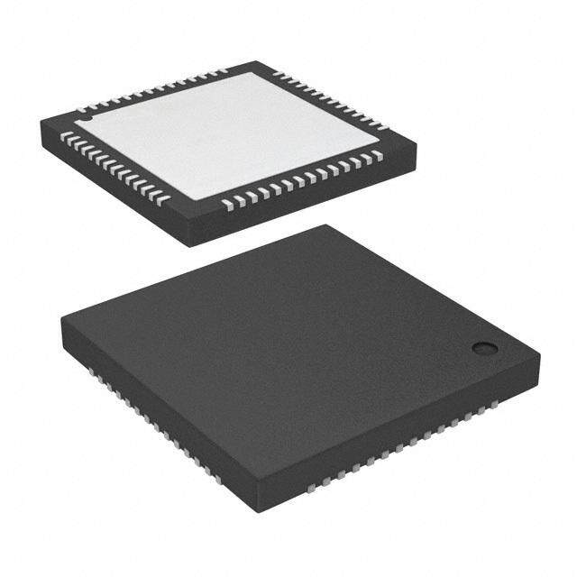
| 供应商器件封装 | 28-PLCC(11.51x11.51) |
| 其它名称 | 428-1708-5 |
| 包装 | 管件 |
| 协议 | 光纤通道 |
| 双工 | - |
| 商标 | Cypress Semiconductor |
| 安装类型 | 表面贴装 |
| 安装风格 | SMD/SMT |
| 封装 | Tube |
| 封装/外壳 | 28-LCC(J 形引线) |
| 封装/箱体 | PLCC-28 |
| 工作温度 | 0°C ~ 70°C |
| 工作电压 | 5 V |
| 工厂包装数量 | 37 |
| 接口类型 | Serial |
| 接收器滞后 | - |
| 数据速率 | - |
| 最大工作温度 | + 70 C |
| 最小工作温度 | 0 C |
| 标准包装 | 74 |
| 电压-电源 | 4.5 V ~ 5.5 V |
| 电源电压-最大 | 5.5 V |
| 电源电压-最小 | 4.5 V |
| 电源电流 | 85 mA |
| 类型 | 接收器 |
| 系列 | CY7B933 |
| 通道数量 | 1 Channel |
| 驱动器/接收器数 | - |


- 商务部:美国ITC正式对集成电路等产品启动337调查
- 曝三星4nm工艺存在良率问题 高通将骁龙8 Gen1或转产台积电
- 太阳诱电将投资9.5亿元在常州建新厂生产MLCC 预计2023年完工
- 英特尔发布欧洲新工厂建设计划 深化IDM 2.0 战略
- 台积电先进制程称霸业界 有大客户加持明年业绩稳了
- 达到5530亿美元!SIA预计今年全球半导体销售额将创下新高
- 英特尔拟将自动驾驶子公司Mobileye上市 估值或超500亿美元
- 三星加码芯片和SET,合并消费电子和移动部门,撤换高东真等 CEO
- 三星电子宣布重大人事变动 还合并消费电子和移动部门
- 海关总署:前11个月进口集成电路产品价值2.52万亿元 增长14.8%


PDF Datasheet 数据手册内容提取
CY7B923/CY7B933 ® HOTLink Transmitter/Receiver Features Functional Description ■Fibre Channel-compliant The CY7B923 HOTLink‚ transmitter and CY7B933 HOTLink receiver are point-to-point communications building blocks that ■IBM ESCON-compliant transfer data over high-speed serial links (fiber, coax, and twisted ■DVB-ASI-compliant pair). Standard HOTLink data rates range from 160 to 330 Mbps. Higher speed HOTLink is also available for high-speed applica- ■ATM-compliant tions (160 to 400 Mbits/second). Figure1 illustrates typical connections to host systems or controllers. ■8B/10B-coded or 10-bit unencoded Eight bits of user data or protocol information are loaded into the ■Standard HOTLink: 160 to 330 Mbps HOTLink transmitter and are encoded. Serial data is shifted out ■High-speed HOTLink: 160 to 400 Mbps for high-speed of the three differential PECL serial ports at the bit rate (which is applications ten times the byte rate). The HOTLink receiver accepts the serial bit stream at its differ- ■Transistor-transistor logic (TTL)-synchronous I/O ential line receiver inputs and, using a completely integrated PLL ■No external phase locked-loop (PLL) components clock synchronizer, recovers the timing information necessary for data reconstruction. The bit stream is deserialized, decoded, ■Triple positive emitter coupled logic (PECL) 100K serial and checked for transmission errors. Recovered bytes are outputs presented in parallel to the receiving host along with a byte-rate ■Dual PECL 100K serial inputs clock. The 8B/10B encoder/decoder can be disabled in systems that ■Low-power: 350 mW (Tx), 650 mW (Rx) already encode or scramble the transmitted data. I/O signals are ■Compatible with fiber-optic modules, coaxial cable, and twisted available to create a seamless interface with both asynchronous pair media FIFOs (that is, CY7C42X) and clocked FIFOs (that is, CY7C44X). A BIST pattern generator and checker allows testing ■Built-in self-test (BIST) of the transmitter, receiver, and the connecting link as a part of a ■Single +5-V supply system diagnostic check. HOTLink devices are ideal for a variety of applications where a ■28-pin small outline integrated circuit (SOIC)/plastic leaded parallel interface can be replaced with a high-speed chip carrier (PLCC) point-to-point serial link. Applications include interconnecting ■Pb-free packages available workstations, servers, mass storage, and video transmission equipment. ■0.8- bipolar complementary metal oxide semiconductor (BiCMOS) CY7B923 Transmitter Block Diagram CypressSemiconductorCorporation • 198 Champion Court • SanJose, CA 95134-1709 • 408-943-2600 Document Number: 38-02017 Rev. *K Revised November 7, 2017
CY7B923/CY7B933 CY7B933 Receiver Block Diagram Figure 1. HOTLink System Connections L O OTOCLOGIC R OCOLGIC R TE E TO P TRANSMIMESSAGBUFFER 7B923TRANSMITT 7B933RECEIVER RECEIVEMESSAGEBUFFER PROL SERIAL LINK HOST HOST Document Number: 38-02017 Rev. *K Page 2 of 42
CY7B923/CY7B933 Contents Pin Configurations ...........................................................4 Receiver Serial Data Requirements ..............................17 Pin Descriptions ...............................................................6 Receiver Test Mode Description ...................................18 CY7B923 HOTLink Transmitter BIST Mode ................................................................18 Block Diagram Description ..............................................8 Test Mode .................................................................18 Input Register ..............................................................8 X3.230 Codes and Notation Conventions ....................18 Encoder .......................................................................8 Notation Conventions ................................................18 Shifter ..........................................................................8 8B/10B Transmission Code .......................................19 OutA, OutB, OutC ........................................................8 Transmission Order ...................................................19 Clock Generator ..........................................................8 Valid and Invalid Transmission Characters ...............19 Test Logic ....................................................................9 Using the Tables for CY7B933 HOTLink Receiver Generating Transmission Characters ...............................20 Block Diagram Description ..............................................9 Using the Tables for Checking the Validity of Serial Data Inputs ........................................................9 Received Transmission Characters ..................................20 PECL-TTL Translator ..................................................9 Valid Data Characters (SC/D = LOW) ............................21 Clock Synchronization .................................................9 Valid Special Character Codes and Sequences Framer .........................................................................9 (SC/D = HIGH)[1, 2] .........................................................29 Shifter ..........................................................................9 Maximum Ratings ...........................................................30 Decode Register ..........................................................9 Operating Range .............................................................30 Decoder .....................................................................10 CY7B923/CY7B933 Electrical Characteristics .............30 Output Register .........................................................10 Capacitance[13] ..............................................................31 Test Logic ..................................................................10 Transmitter Switching Characteristics .........................32 HOTLink CY7B923 Transmitter and CY7B933 Receiver Switching Characteristics ..............................33 Receiver Operation .........................................................10 Switching Waveforms ....................................................34 CY7B923 HOTLink Transmitter Ordering Information ......................................................37 Operating Mode Description .........................................11 Ordering Code Definitions .........................................37 Encoded Mode Operation .........................................12 Package Diagrams ..........................................................38 Bypass Mode Operation ............................................13 Acronyms ........................................................................40 PECL Output Functional and Connection Options ....13 Document Conventions .................................................40 Transmitter Serial Data Characteristics .......................13 Units of Measure .......................................................40 Transmitter Test Mode Description ..............................13 Document History Page .................................................41 BIST Mode ................................................................15 Sales, Solutions, and Legal Information ......................42 Test Mode .................................................................16 Worldwide Sales and Design Support .......................42 CY7B933 HOTLink Receiver Products ....................................................................42 Operating Mode Description .........................................16 PSoC® Solutions ......................................................42 Encoded Mode Operation .........................................16 Cypress Developer Community .................................42 Bypass Mode Operation ............................................17 Technical Support .....................................................42 Parallel Output Function ............................................17 Document Number: 38-02017 Rev. *K Page 3 of 42
CY7B923/CY7B933 Pin Configurations Figure 2. CY7B923 Transmitter Pin Configurations SOIC Top View OUTB 1 28 OUTB+ OUTC 2 27 OUTA+ OUTC+ 3 26 OUTA VCCN 4 25 FOTO BISTEN 5 24 ENN GND 6 23 ENA MODE 7 7B923 22 VCCQ RP 8 21 CKW VCCQ 9 20 GND SVS(Dj) 10 19 SC/D(Da) (Dh)D7 11 18 D0(Db) (Dg)D6 12 17 D1(Dc) (Df)D5 13 16 D2(Dd) (Di)D4 14 15 D3(De) PLCC/LCC Top View +++ CCBBAA NTTTTTT VCCOUOUOUOUOUOU 4 3 2 1 282726 BISTEN 5 25 FOTO GND 6 24 ENN MODE 7 23 ENA RP 8 7B923 22 VCCQ VCCQ 9 21 CKW SVS(Dj) 10 20 GND (Dh)D7 111213 141516171819 SC/D(Da) 6543210 DDDDDDD D )gD )fD )iD )eD )dD )cD )b ((((((( Document Number: 38-02017 Rev. *K Page 4 of 42
CY7B923/CY7B933 Figure 3. CY7B933 Receiver Pin Configurations SOIC Top View INA 1 28 INB(INB+) INA+ 2 27 SI(INB ) A/B 3 26 MODE BISTEN 4 25 REFCLK RF 5 24 VCCQ GND 6 23 SO RDY 7 22 CKR 7B933 GND 8 21 VCCQ VCCN 9 20 GND RVS(Qj) 10 19 SC/D(Qa) (Qh)Q7 11 18 Q0(Qb) (Qg)Q6 12 17 Q1(Qc) (Qf)Q5 13 16 Q2(Qd) (Qi)Q4 14 15 Q3(Qe) PLCC/LCC Top View +) BISTENA/BNA+NANB (INBSI (INB)MODE III 4 3 2 1 282726 RF 5 25 REFCLK GND 6 24 VCCQ RDY 7 23 SO 7B933 GND 8 22 CKR VCCN 9 21 VCCQ RVS(Qj) 10 20 GND (Qh)Q7 111213141516171819 SC/D(Qa) 6 543210 QQQQQQQ Q )gQ )fQ )iQ )eQ )dQ )cQ )b ((((((( Document Number: 38-02017 Rev. *K Page 5 of 42
CY7B923/CY7B933 Pin Descriptions Table 1. CY7B923 HOTLink Transmitter Name I/O Description D TTL In Parallel data input. Data is clocked into the Transmitter on the rising edge of CKW if ENA is LOW (or on 07 (D ) the next rising CKW with ENN LOW). If ENA and ENN are HIGH, a Null character (K28.5) is sent. When b h MODE is HIGH, D become D , respectively. 0, 1, ...7 b, c,...h SC/D (D ) TTL In Special character/data select. A HIGH on SC/D when CKW rises causes the transmitter to encode the a pattern on D as a control code (Special Character), while a LOW causes the data to be coded using 07 the 8B/10B data alphabet. When MODE is HIGH, SC/D (D ) acts as D input. SC/D has the same timing a a as D . 07 SVS TTL In Send violation symbol. If SVS is HIGH when CKW rises, a Violation symbol is encoded and sent while (D) the data on the parallel inputs is ignored. If SVS is LOW, the state of D and SC/D determines the code j 07 sent. In normal or test mode, this pin overrides the BIST generator and forces the transmission of a Violation code. When MODE is HIGH (placing the transmitter in unencoded mode), SVS (D) acts as the j D input. SVS has the same timing as D . j 07 ENA TTL In Enable parallel data. If ENA is LOW on the rising edge of CKW, the data is loaded, encoded, and sent. If ENA and ENN are HIGH, the data inputs are ignored and the Transmitter will insert a Null character (K28.5) to fill the space between user data. ENA may be held HIGH/LOW continuously or it may be pulsed with each data byte to be sent. If ENA is being used for data control, ENN will normally be strapped HIGH, but can be used for BIST function control. ENN TTL In Enable next parallel data. If ENN is LOW, the data appearing on D at the next rising edge of CKW is 07 loaded, encoded, and sent. If ENA and ENN are HIGH, the data appearing on D at the next rising edge 07 of CKW will be ignored and the Transmitter will insert a Null character to fill the space between user data. ENN may be held HIGH/LOW continuously or it may be pulsed with each data byte sent. If ENN is being used for data control, ENA will normally be strapped HIGH, but can be used for BIST function control. CKW TTL In Clock write. CKW is both the clock frequency reference for the multiplying PLL that generates the high-speed transmit clock, and the byte rate write signal that synchronizes the parallel data input. CKW must be connected to a crystal controlled time base that runs within the specified frequency range of the Transmitter and Receiver. FOTO TTL In Fiber optic transmitter off. FOTO determines the function of two of the three PECL transmitter output pairs. If FOTO is LOW, the data encoded by the Transmitter will appear at the outputs continuously. If FOTO is HIGH, OUTA and OUTB are forced to their “logic zero” state (OUT+ = LOW and OUT = HIGH), causing a fiber-optic transmit module to extinguish its light output. OUTC is unaffected by the level on FOTO, and can be used as a loop-back signal source for board-level diagnostic testing. OUTA PECL Out Differential serial data outputs. These PECL 100K outputs (+5V referenced) are capable of driving OUTB terminated transmission lines or commercial fiber optic transmitter modules. Unused pairs of outputs can OUTC be left open, or wired to V to reduce power, if the output is not required. OUTA± and OUTB± are CC controlled by the level on FOTO, and will remain at their “logical zero” states when FOTO is asserted. OUTC± is unaffected by the level on FOTO. (OUTA+ and OUTB+ are used as a differential test clock input while in Test mode, that is, MODE = UNCONNECTED or forced to V /2). CC MODE Three- Encoder mode select. The level on MODE determines the encoding method to be used. When wired to Level In GND, MODE selects 8B/10B encoding. When wired to V , data inputs bypass the encoder and the bit CC pattern on D goes directly to the shifter. When left floating (internal resistors hold the input at V /2) a–j CC the internal bit-clock generator is disabled and OUTA+/OUTB+ become the differential bit clock to be used for factory test. In typical applications MODE is wired to V or GND. CC BISTEN TTL In BIST enable. When BISTEN is LOW and ENA and ENN are HIGH, the transmitter sends an alternating 1–0 pattern (D10.2 or D21.5). When either ENA or ENN is set LOW and BISTEN is LOW, the transmitter begins a repeating test sequence that allows the Transmitter and Receiver to work together to test the function of the entire link. In normal use this input is held HIGH or wired to V . The BIST generator is a CC free-running pattern generator that need not be initialized, but if required, the BIST sequence can be initialized by momentarily asserting SVS while BISTEN is LOW. BISTEN has the same timing as D . 0-7 RP TTL Out Read pulse. RP is a 60% LOW duty-cycle byte-rate pulse train suitable for the read pulse in CY7C42X FIFOs. The frequency on RP is the same as CKW when enabled by ENA, and duty cycle is independent of the CKW duty cycle. Pulse widths are set by logic internal to the transmitter. In BIST mode, RP will remain HIGH for all but the last byte of a test loop. RP will pulse LOW one byte time per BIST loop. V Power for output drivers. CCN V Power for internal circuitry. CCQ GND Ground. Document Number: 38-02017 Rev. *K Page 6 of 42
CY7B923/CY7B933 Table 2. CY7B933 HOTLink Receiver Name I/O Description Q TTL Out Q parallel data output. Q contain the most recently received data. These outputs change synchro- 07 0–7 0–7 (Q ) nously with CKR. When MODE is HIGH, Q become Q , respectively. b h 0, 1, ...7 b, c,...h SC/D(Q ) TTL Out Special character/data select. SC/D indicates the context of received data. HIGH indicates a Control a (Special Character) code, LOW indicates a Data character. When MODE is HIGH (placing the receiver in Unencoded mode), SC/D acts as the Q output. SC/D has the same timing as Q . a 07 RVS(Q) TTL Out Received violation symbol. A HIGH on RVS indicates that a code rule violation has been detected in the j received data stream. A LOW shows that no error has been detected. In BIST mode, a LOW on RVS indicates correct operation of the Transmitter, Receiver, and link on a byte-by-byte basis. When MODE is HIGH (placing the receiver in Unencoded mode), RVS acts as the Q output. RVS has the same timing j as Q . 07 RDY TTL Out Data output ready. A LOW pulse on RDY indicates that new data has been received and is ready to be delivered. A missing pulse on RDY shows that the received data is the Null character (normally inserted by the transmitter as a pad between data inputs). In BIST mode RDY will remain LOW for all but the last byte of a test loop and will pulse HIGH one byte time per BIST loop. CKR TTL Out Clock read. This byte rate clock output is phase and frequency aligned to the incoming serial data stream. RDY, Q , SC/D, and RVS all switch synchronously with the rising edge of this output. 07 A/B PECL in Serial data input select. This PECL 100K (+5V referenced) input selects INA or INB as the active data input. If A/B is HIGH, INA is connected to the shifter and signals connected to INA will be decoded. If A/B is LOW INB is selected. INA Diff In Serial data input A. The differential signal at the receiver end of the communication link may be connected to the differential input pairs INA or INB. Either the INA pair or the INB pair can be used as the main data input and the other can be used as a loopback channel or as an alternative data input selected by the state of A/B. One input of an intentionally unused differential-pair (INA or INBshould be terminated to V through a 15-K resistor to assure that no data transitions are accidentally created. CC INB PECL in Serial data input B. This pin is either a single-ended PECL data receiver (INB) or half of the INB differential (INB+) (Diff In) pair. If SO is wired to V , then INB can be used as differential line receiver interchangeably with INA. CC If SO is normally connected and loaded, INB becomes a single-ended PECL 100K (+5V referenced) serial data input. INB is used as the test clock while in Test mode. SI PECL in Status input. This pin is either a single-ended PECL status monitor input (SI) or half of the INB differential (INB) (Diff In) pair. If SO is wired to V , then INB can be used as differential line receiver interchangeably with INA. CC If SO is normally connected and loaded, SI becomes a single-ended PECL 100K (+5V referenced) status monitor input, which is translated into a TTL-level signal at the SO pin. SO TTL Out Status out. SO is the TTL-translated output of SI. It is typically used to translate the carrier detect output from a fiber-optic receiver connected to SI. When this pin is normally connected and loaded (without any external pull-up resistor), SO will assume the same logical level as SI and INB will become a single-ended PECL serial data input. If the status monitor translation is not desired, then SO may be wired to V and CC the INB pair may be used as a differential serial data input. RF TTL In Reframe enable. RF controls the Framer logic in the Receiver. When RF is held HIGH, each SYNC (K28.5) symbol detected in the shifter will frame the data that follows. If it is HIGH for 2,048 consecutive bytes, the internal framer switches to double-byte mode. When RF is held LOW, the reframing logic is disabled. The incoming data stream is then continuously deserialized and decoded using byte boundaries set by the internal byte counter. Bit errors in the data stream will not cause alias SYNC characters to reframe the data erroneously. REFCLK TTL In Reference clock. REFCLK is the clock frequency reference for the clock/data synchronizing PLL. REFCLK sets the approximate center frequency for the internal PLL to track the incoming bit stream. REFCLK must be connected to a crystal-controlled time base that runs within the frequency limits of the Tx/Rx pair, and the frequency must be the same as the transmitter CKW frequency (within CKW0.1%). MODE Three- Decoder mode select. The level on the MODE pin determines the decoding method to be used. When Level In wired to GND, MODE selects 8B/10B decoding. When wired to V , registered shifter contents bypass CC the decoder and are sent to Q directly. When left floating (internal resistors hold the MODE pin at V /2) aj CC the internal bit clock generator is disabled and INB becomes the bit rate test clock to be used for factory test. In typical applications, MODE is wired to V or GND. CC Document Number: 38-02017 Rev. *K Page 7 of 42
CY7B923/CY7B933 Table 2. CY7B933 HOTLink Receiver (continued) Name I/O Description BISTEN TTL In Built-in self-test enable. When BISTEN is LOW the Receiver awaits a D0.0 (sent once per BIST loop) character and begins a continuous test sequence that tests the functionality of the Transmitter, the Receiver, and the link connecting them. In BIST mode the status of the test can be monitored with RDY and RVS outputs. In normal use BISTEN is held HIGH or wired to V . BISTEN has the same timing as CC Q . 0–7 V Power for output drivers. CCN V Power for internal circuitry. CCQ GND Ground. CY7B923 HOTLink Transmitter Block the bit order is specified in the fibre channel 8B/10B code) Diagram Description become the ten inputs to the shifter, with Da being the first bit to be shifted out. Input Register Shifter The input register holds the data to be processed by the HOTLink The shifter accepts parallel data from the encoder after each byte transmitter and allows the input timing to be made consistent with time and shifts it to the serial interface output buffers using a PLL standard FIFOs. The input register is clocked by CKW and multiplied bit clock that runs at 10 times the byte clock rate. loaded with information on the D , SC/D, and SVS pins. Two 0-7 Timing for the parallel transfer is controlled by the counter enable inputs (ENA and ENN) allow the user to choose when included in the clock generator and is not affected by signal data is loaded in the register. Asserting Enable, active LOW levels or timing at the input pins. (ENA) causes the inputs to be loaded in the register on the rising edge of CKW. If ENN (Enable Next, active LOW) is asserted OutA, OutB, OutC when CKW rises, the data present on the inputs on the next rising edge of CKW are loaded into the Input register. If neither ENA The serial interface PECL output buffers (ECL100K referenced nor ENN are asserted LOW on the rising edge of CKW, then a to +5V) are the drivers for the serial media. They are all SYNC (K28.5) character is sent. These two inputs allow proper connected to the shifter and contain the same serial data. Two of timing and function for compatibility with either asynchronous the output pairs (OUTA± and OUTB±) are controllable by the FOTO input and can be disabled by the system controller to force FIFOs or clocked FIFOs without external logic, as shown in Figure6. a logical zero (that is, “light off”) at the outputs. The third output pair (OUTC±) is not affected by FOTO and supplies a continuous In BIST mode, the input register becomes the signature pattern data stream suitable for loopback testing of the subsystem. generator by logically converting the parallel input register into a OUTA± and OUTB± responds to FOTO input changes within a linear feedback shift register (LFSR). When enabled, this LFSR few bit times. However, since FOTO is not synchronized with the generates a 511-byte sequence that includes all data and special transmitter data stream, the outputs will be forced off or turned character codes, including the explicit violation symbols. This on at arbitrary points in a transmitted byte. This function is pattern provides a predictable but pseudo-random sequence that intended to augment an external laser safety controller and as can be matched to an identical LFSR in the receiver. an aid for Receiver PLL testing. Encoder In wire-based systems, control of the outputs may not be The encoder transforms the input data held by the input register required, and FOTO can be strapped LOW. The three outputs into a form more suitable for transmission on a serial interface are intended to add system and architectural flexibility by offering link. The code used is specified by ANSI X3.230 (Fibre Channel) identical serial bit streams with separate interfaces for redundant and the IBM ESCON channel (see the table Valid Data connections or for multiple destinations. Unneeded outputs can Characters (SC/D = LOW) on page 21). The eight D data be wired to VCC to disable and power down the unused output 0–7 inputs are converted to either a data symbol or a special circuitry. character, depending upon the state of the SC/D input. If SC/D Clock Generator is HIGH, the data inputs represent a control code and are encoded using the special character code table. If SC/D is LOW, The clock generator is an embedded PLL that takes a byte-rate the data inputs are converted using the data code table. If a byte reference clock (CKW) and multiplies it by 10 to create a bit rate time passes with the inputs disabled, the encoder outputs a clock for driving the serial shifter. The byte rate reference comes special character comma K28.5 (or SYNC) that maintains link from CKW, the rising edge of which clocks data into the input synchronization. SVS input forces the transmission of a specified register. This clock must be a crystal referenced pulse stream violation symbol to allow the user to check the error handling that has a frequency between the minimum and maximum system logic in the controller or for proprietary applications. specified for the HOTLink transmitter/receiver pair. Signals The 8B/10B coding function of the encoder can be bypassed for controlled by this block form the bit clock and the timing signals that control internal data transfers between the input register and systems that include an external coder or scrambler function as part of the controller. This bypass is controlled by setting the the shifter. MODE select pin HIGH. When in bypass mode, D (note that a-j Document Number: 38-02017 Rev. *K Page 8 of 42
CY7B923/CY7B933 The read pulse (RP) is derived from the feedback counter used serial data transitions. This block contains the logic to transfer in the PLL multiplier. It is a byte-rate pulse stream with the proper the data from the shifter to the decode register once every byte. phase and pulse widths to allow transfer of data from an The counter that controls this transfer is initialized by the framer asynchronous FIFO. Pulse width is independent of CKW duty logic. CKR is a buffered output derived from the bit counter used cycle, since proper phase and duty cycle is maintained by the to control the decode register and the output register transfers. PLL. The RP pulse stream ensures correct data transfers Clock output logic is designed so that when reframing causes the between asynchronous FIFOs and the transmitter input latch counter sequence to be interrupted, the period and pulse width with no external logic. of CKR is never less than normal. Reframing may stretch the period of CKR by up to 90%, and either CKR Pulse Width HIGH Test Logic or Pulse Width LOW may be stretched, depending on when Test logic includes the initialization and control for the BIST reframe occurs. generator, the multiplexer for test mode clock distribution, and The REFCLK input provides a byte-rate reference frequency to control logic to properly select the data encoding. Test logic is improve PLL acquisition time and limit unlocked frequency discussed in detail in CY7B923 HOTLink Transmitter Operating excursions of the CKR when no data is present at the serial Mode Description on page 11. inputs. The frequency of REFCLK is required to be within ±0.1% CY7B933 HOTLink Receiver Block Diagram of the frequency of the clock that drives the transmitter CKW pin. Description Framer Framer logic checks the incoming bit stream for the pattern that Serial Data Inputs defines the byte boundaries. This combinatorial logic filter looks Two pairs of differential line receivers are the inputs for the serial for the X3.230 symbol defined as a Special Character Comma data stream. INA± or INB± can be selected with the A/B input. (K28.5). When it is found, the free-running bit counter in the INA± is selected with A/B HIGH and INB± is selected with A/B Clock Synchronization block is synchronously reset to its initial LOW. The threshold of A/B is compatible with the ECL 100K state, thus framing the data correctly on the correct byte bound- signals from PECL fiber optic interface modules. TTL logic aries. elements can be used to select the A or B inputs by adding a Random errors that occur in the serial data can corrupt some resistor pull-up to the TTL driver connected to A/B. The data patterns into a bit pattern identical to a K28.5, and thus differential threshold of INA± and INB± will accommodate wire cause an erroneous data-framing error. The RF input prevents interconnect with filtering losses or transmission line attenuation this by inhibiting reframing during times when normal message greater than 20 db (V > 50 mv) or can be directly connected DIF data is present. When RF is held LOW, the HOTLink receiver will to fiber optic interface modules (any ECL logic family, not limited deserialize the incoming data without trying to reframe the data to ECL 100K). The common mode tolerance will accommodate to incoming patterns. When RF rises, RDY will be inhibited until a wide range of signal termination voltages. The highest HIGH a K28.5 has been detected, after which RDY will resume its input that can be tolerated is V = V , and the lowest LOW IN CC normal function. While RF is HIGH, it is possible that an error input that can be interpreted correctly is V = GND+2.0V. IN could cause misframing, after which all data will be corrupted. PECL-TTL Translator Likewise, a K28.7 followed by D11.x, D20.x, or an SVS (C0.7) followed by D11.x will create alias K28.5 characters and cause The function of the INB(INB+) input and the SI(INB–) input is erroneous framing. These sequences must be avoided while RF defined by the connections on the SO output pin. If the is HIGH. PECL/TTL translator function is not required, the SO output is If RF remains HIGH for greater than 2048 bytes, the framer wired to VCC. A sensor circuit detects this connection and converts to double-byte framing, requiring two K28.5 characters causes the inputs to become INB± (a differential line-receiver aligned on the same byte boundary within 5 bytes in order to serial-data input). If the PECL/TTL translator function is required, reframe. Double-byte framing greatly reduces the possibility of the SO output is connected to its normal TTL load (typically one erroneously reframing to an aliased K28.5 character. or more TTL inputs, but no pull-up resistor) and the INB+ input becomes single-ended ECL 100K, serial data input (INB) and the Shifter INB– input becomes single-ended, ECL 100K status input (SI). The shifter accepts serial inputs from the serial data inputs one This positive-referenced PECL-to-TTL translator is provided to bit at a time, as clocked by the clock synchronization logic. Data eliminate external logic between an PECL fiber-optic interface is transferred to the framer on each bit, and to the decode module “carrier detect” output and the TTL input in the control register once per byte. logic. The input threshold is compatible with ECL 100K levels (+5-V referenced). It can also be used as part of the link status Decode Register indication logic for wire connected systems. The decode register accepts data from the shifter once per byte Clock Synchronization as determined by the logic in the clock synchronization block. It is presented to the decoder and held until it is transferred to the The clock synchronization function is performed by an output latch. embedded PLL that tracks the frequency of the incoming bit stream and aligns the phase of its internal bit rate clock to the Document Number: 38-02017 Rev. *K Page 9 of 42
CY7B923/CY7B933 Decoder HOTLink CY7B923 Transmitter and CY7B933 Parallel data is transformed from ANSI-specified X3.230 8B/10B Receiver Operation codes back to ‘raw data’ in the decoder. This block uses the standard decoder patterns shown in Valid Data Characters The CY7B923 Transmitter operating with the CY7B933 Receiver (SC/D = LOW) on page 21 and Valid Special Character Codes form a general purpose data communications subsystem and Sequences (SC/D = HIGH)[1, 2] on page 29. Data patterns capable of transporting user data at up to 33 Mbytes per second are signaled by a LOW on the SC/D output and special character (40 Mbytes per second for –400 devices) over several types of patterns are signaled by a HIGH on the SC/D output. Unused serial interface media. Figure 10 on page 34 illustrates the flow patterns or disparity errors are signaled as errors by a HIGH on of data through the HOTLink CY7B923 transmitter pipeline. Data the RVS output and by specific special character codes. is latched into the transmitter on the rising edge of CKW when enabled by ENA or ENN. RP is asserted LOW with a 60% Output Register LOW/40% HIGH duty cycle when ENA is LOW. RP may be used as a read strobe for accessing data stored in a FIFO. The parallel The output register holds the recovered data (Q , SC/D, and 0–7 data flows through the encoder and is then shifted out of the RVS) and aligns it with the recovered byte clock (CKR). This OUTx± PECL drivers. The bit-rate clock is generated internally synchronization insures proper timing to match a FIFO interface from a multiply-by-ten PLL clock generator. The latency through or other logic that requires glitch-free and specified output the transmitter is approximately 21t – 10 ns over the operating behavior. Outputs change synchronously with the rising edge of B range. A more complete description is found in the section CKR. CY7B923 HOTLink Transmitter Operating Mode Description. In BIST mode, this register becomes the signature pattern Figure5 illustrates the data flow through the HOTLink CY7B933 generator and checker by logically converting itself into a linear receiver pipeline. Serial data is sampled by the receiver on the feedback shift register (LFSR) pattern generator. When enabled, INx± inputs. The receiver PLL locks onto the serial bit stream and this LFSR generates a 511-byte sequence that includes all data generates an internal bit rate clock. The bit stream is deseri- and special character codes, including the explicit violation alized, decoded and then presented at the parallel output pins. symbols. This pattern provides a predictable but pseudo-random A byte rate clock (bit clock 10) synchronous with the parallel sequence that can be matched to an identical LFSR in the Trans- data is presented at the CKR pin. The RDY pin will be asserted mitter. When synchronized, it checks each byte in the Decoder to LOW to indicate that data or control characters are present on with each byte generated by the LFSR and shows errors at RVS. the outputs. RDY will not be asserted LOW in a field of K28.5s Patterns generated by the LFSR are compared after being except for any single K28.5 or the last one in a continuous series buffered to the output pins and then fed back to the comparators, of K28.5’s. The latency through the receiver is approximately allowing test of the entire receive function. 24t + 10 ns over the operating range. A more complete B In BIST mode, the LFSR is initialized by the first occurrence of description of the receiver is in the section CY7B933 HOTLink the transmitter BIST loop start code D0.0 (D0.0 is sent only once Receiver Operating Mode Description. per BIST loop). Once the BIST loop has been started, RVS will The HOTLink receiver has a built-in byte framer that synchro- be HIGH for pattern mismatches between the received sequence nizes the Receiver pipeline with incoming SYNC (K28.5) and the internally generated sequence. Code rule violations or characters. Figure5 illustrates the HOTLink CY7B933 Receiver running disparity errors that occur as part of the BIST loop will framing operation. The Framer is enabled when the RF pin is not cause an error indication. RDY will pulse HIGH once per asserted HIGH. RF is latched into the receiver on the falling edge BIST loop and can be used to check test pattern progress. The of CKR. The framer looks for K28.5 characters embedded in the receiver BIST generator can be reinitialized by leaving and serial data stream. When a K28.5 is found, the framer sets the re-entering BIST mode. parallel byte boundary for subsequent data to the K28.5 Test Logic boundary. While the framer is enabled, the RDY pin indicates the status of the framing operation. Test logic includes the initialization and control for the Built-In Self-Test (BIST) generator, the multiplexer for Test mode clock When the RF pin is asserted HIGH, RDY leaves it normal mode distribution, and control logic for the decoder. Test logic is of operation and is asserted HIGH while the framer searches the data stream for a K28.5 character. After the framer has synchro- discussed in more detail in the CY7B933 HOTLink Receiver Operating Mode Description. nized to a K28.5 character, the Receiver will assert the RDY pin LOW when the K28.5 character is present at the parallel output. The RDY pin will then resume its normal operation as dictated by the MODE and BISTEN pins. The normal operation of the RDY pin in encoded mode is to signal when parallel data is present at the output pins by pulsing LOW with a 60% LOW/40% HIGH duty cycle. RDY does not pulse LOW in a field of K28.5 characters; however, RDY does pulse LOW for the last K28.5 character in the field or for any single K28.5. In unencoded mode, the normal operation of the RDY pin is to signal when any K28.5 is at the parallel output pins. Document Number: 38-02017 Rev. *K Page 10 of 42
CY7B923/CY7B933 Figure 4. CY7B933 Receiver Data Pipeline in Encoded Mode SERIAL DATA IN RECEIVER LATENCY= 24tB+10ns INX DATA CKR Q , 07 SC/D, DATA K28.5 K28.5 DATA RVS RDY RDY IS HIGH IN FIELD OF K28.5S RDYIS LOW FOR DATA RDYIS LOW FOR LAST K28.5 PARALLEL DATA OUT Figure 5. CY7B933 Framing Operation in Encoded Mode RFLATCHEDON CKR STRETCHES AS FALLING EDGE OF CKR DATA BOUNDARY CHANGES CKR RF Q , 07 SC/D, DATA DATA DATA DATA DATA K28.5 DATA DATA RVS RDY RDY IS HIGH WHILE WAITING FOR K28.5 RDYISLOW RDY RESUMES FOR K28.5 NORMAL OPERATION The transmitter and receiver parallel interface timing and CY7B923 HOTLink Transmitter Operating functionality can be made to match the timing and functionality Mode Description of either an asynchronous FIFO or a clocked FIFO by appropri- ately connecting signals (see Figure 6 on page 12). Proper In normal operation, the transmitter can operate in either of two operation of the FIFO interface depends upon various modes. The encoded mode allows a user to send and receive FIFO-specific access and response specifications. eight-bit data and control information without first converting it to The HOTLink transmitter and receiver serial interface provides a transmission characters. The bypass mode is used for systems seamless interface to various types of media. A minimal number in which the encoding and decoding is performed in an external of external components are needed to properly terminate trans- protocol controller. mission lines and provide PECL loads. For proper power supply In either mode, data is loaded into the Input register of the Trans- decoupling, a single 0.01 F for each device is all that is required mitter on the rising edge of CKW. The input timing and functional to bypass the V and GND pins. Figure 7 on page 14 illustrates CC response of the Transmitter input can be made to match the a HOTLink transmitter and receiver interface to fiber-optic and timing and functionality of either an asynchronous FIFO or a copper media. More information on interfacing HOTLink to clocked FIFO by an appropriate connection of input signals (see various media can be found in the HOTLink Design Consider- Figure 6 on page 12). Proper operation of the FIFO interface ations application note. depends upon various FIFO-specific access and response specifications. Document Number: 38-02017 Rev. *K Page 11 of 42
CY7B923/CY7B933 Encoded Mode Operation The diagnostic characters and sequences available as special characters include those for Fibre Channel link testing, as well In the encoded mode, the input data is interpreted as eight bits as codes to be used for testing system response to link errors of data (D –D ), a context control bit (SC/D), and a system 0 7 and timing. A Violation symbol can be explicitly sent as part of a diagnostic input bit (SVS). If the context of the data is to be user data packet (i.e., send C0.7; D = 111 00000 and SC/D = normal message data, the SC/D input should be LOW, and the 7–0 1), or it can be sent in response to an external system using the data should be encoded using the valid data character set SVS input. This allows the system diagnostic logic to evaluate described in Valid Data Characters (SC/D = LOW) on page 21. the errors in an unambiguous manner, and does not require any If the context of the data is to be control or protocol information, modification to the transmission interface to force transmission the SC/D input is HIGH, and the data is encoded using the valid errors for testing purposes. special character set described in Valid Special Character Codes and Sequences (SC/D = HIGH)[1, 2] on page 29. Special characters include all protocol characters necessary to encode packets for Fibre Channel, ESCON, proprietary systems, and diagnostic purposes. Figure 6. Seamless FIFO Interface ASYNCHRONOUS FIFO CLOCKED FIFO 7C42X/3X/6X/7X 7C44X/5X R LE R Q0–8 ENR CKR Q0–8 L O R 9 T N 9 O C M O R F ENA CKW RP D0–7, SC/D ENN CKW D0–7, SC/D 7B923 7B923 HOTLink TRANSMITTER HOTLink TRANSMITTER HOTLink RECEIVER HOTLink RECEIVER 7B933 7B933 CKR RDY Q0–7, SC/D CKR RDY Q0–7, SC/D 9 9 W D0–8 CKW ENW D0–8 7C42X/3X/6X/7X 7C44X/5X ASYNCHRONOUS FIFO CLOCKED FIFO Document Number: 38-02017 Rev. *K Page 12 of 42
CY7B923/CY7B933 Bypass Mode Operation In systems that require the outputs to be shut off during some periods when link transmission is prohibited (for example, for In the bypass mode, the input data is interpreted as 10 bits laser safety functions), the FOTO input can be asserted. While it (D ), SC/D (D ), and SVS (D) of pre-encoded transmission b–h a j is possible to insure that the output state of the PECL drivers is data to be serialized and sent over the link. This data can use LOW (that is, light is off) by sending all 0s in bypass mode, it is any encoding method suitable to the designer. The only restric- often inconvenient to insert this level of control into the data tions upon the data encoding method is that it contain suitable transmission channel, and it is impossible in encoded mode. transition density for the receiver PLL data synchronizer (one per FOTO is provided to simplify and augment this control function 10-bit byte), and that it be compatible with the transmission (typically found in laser-based transmission systems). FOTO will media. force OUTA+ and OUTB+ to go LOW, OUTA– and OUTB– to go Data loaded into the Input register on the rising edge of CKW is HIGH, while allowing OUTC± to continue to function normally loaded into the shifter on the subsequent rising edges of CKW. (OUTC is typically used as a diagnostic feedback and cannot be It will then be shifted to the outputs one bit at a time using the disabled). This separation of function allows various system internal clock generated by the clock generator. The first bit of configurations without undue load on the control function or data the transmission character (Da) appears at the output (OUTA±, channel logic. OUTB±, and OUTC±) after the next CKW edge. Transmitter Serial Data Characteristics While in either the encoded mode or bypass mode, if a CKW edge arrives when the inputs are not enabled (ENA and ENN The CY7B923 HOTLink transmitter serial output conforms to the both HIGH), the encoder inserts a pad character K28.5 (for requirements of the Fibre Channel specification. The serial data example, C5.0) to maintain proper link synchronization (in the output is controlled by an internal PLL that multiplies the bypass mode the proper sense of running disparity cannot be frequency of CKW by 10 to maintain the proper bit clock guaranteed for the first pad character, but is correct for all pad frequency. The jitter characteristics (including both PLL and logic characters that follow). This automatic insertion of pad components) are as follows: characters can be inhibited by insuring that the transmitter is always enabled (that is, ENA or ENN is hard-wired LOW). ■Deterministic Jitter (D) < 35 ps (peak-peak). Typically j measured while sending a continuous K28.5 (C5.0). PECL Output Functional and Connection Options ■Random Jitter (R) < 175 ps (peak-peak). Typically measured The three pairs of PECL outputs all contain the same information j while sending a continuous K28.7 (C7.0). and are intended for use in systems with multiple connections. Each output pair may be connected to a different serial media, Transmitter Test Mode Description each of which may be a different length, link type, or interface technology. For systems that do not require all three output pairs, The CY7B923 transmitter offers two types of test mode the unused pairs should be wired to V to minimize the power CC operation, BIST mode and Test mode. In a normal system appli- dissipated by the output circuit, and to minimize unwanted noise cation, the BIST mode can be used to check the functionality of generation. An internal voltage comparator detects when an the transmitter, the receiver, and the link connecting them. This output differential pair is wired to V , causing the current source CC mode is available with minimal impact on user system logic, and for that pair to be disabled. This results in a power savings of can be used as part of the normal system diagnostics. Typical around 5 mA for each unused pair. connections and timing are shown in Figure 8 on page 15. Document Number: 38-02017 Rev. *K Page 13 of 42
CY7B923/CY7B933 Figure 7. HOTLink Connection Diagram 0.01 F 4 922 Config 7 MODE VCC Tx PECL Load 0.01 F CSotanttaruonsld 22285435 EEBFOINNSTNATOECNY7BOO9UU2TT3AA–+ 2267 BA 8822 113300 TTXXF–+VibTCeXCr FiberT Oxptic 111978 RSDCP0/(DDTb(rD)aan)smOOiUUtteTTrBB–+ 218UOtonp uMesnien diom rO iWzuetip rPeudot wLtoee frVt DCCissipa0t.io0n1 F GND Data 1111123456 DDDDD54321(((((DDDDDfedic))))) OOUUTTCC–+ 23 Tx PEC22L77 00Load A TwCisoteadx oPrair 11 D6(Dg) B 1201 SDV7S(D(Dh)j) 270 270 CKW GND 0.01 F 620 649 1500 Transmission RL/2 Line Coax or Termination 0.01 F C Twisted Pair 92124 RL/2 26 VCC Config 25 MODE D REFCLK 423 BISTEN E SOigpntaiol nDaelt. Control 3 SO CY7B933 and 5 A/B Receiver Status 7 RRDFY IB+ 2278 E IB– 1198 SC/D(Qa) 270 0.01 F 1167 DD10((QQbc)) 82 130 FVibCeCr Fiber Optic 1145 DD32((QQde)) IA+ 12 DC SRIXG+RX Rx Data 1123 DD54((QQfi)) IA– 82 130 RX–GND 11 D6(Qg) 10 D7(Qh) 0.01 F 22 RVS(Qj) CKR GND Fiber Optic 6 8 20 PECL Load Document Number: 38-02017 Rev. *K Page 14 of 42
CY7B923/CY7B933 Figure 8. BIST Illustration CY7B923 DON'T CARE FOTO DON'T CARE MODE BIST WITHIN SPEC. LOOP CKW RP DON'T CARE SC/D OUTA DON'T CARE D 8 0–7 OUTB LOW SVS OUTC ENA HIGH Tx Tx ENN START STOP BISTEN CY7B933 WITHIN SPEC. REFCLK DON'T CARE MODE LOW RF SO CKR DON'T CARE SC/D INA Q 0–7 8 ERROR INB RVS LOW TEST BIST A/B START LOOP RDY BISTEN Rx TEST BEGIN END TEST BIST Mode BIST loop, and can be used by an external counter to monitor the number of test pattern loops. The BIST mode functions as follows: 4.When testing is completed, set BISTEN HIGH and ENA and 1.Set BISTEN LOW to begin test pattern generation. The trans- ENN HIGH and resume normal function. mitter begins sending bit rate ...1010... Note: It may be advisable to send violation characters to test the 2.Set either ENA or ENN LOW to begin pattern sequence RVS output in the receiver. This can be done by explicitly generation (use of the Enable pin not being used for normal sending a violation with the SVS input, or allowing the transmitter FIFO or system interface can minimize logic delays between BIST loop to run while the receiver runs in normal mode. The the controller and transmitter). BIST loop includes deliberate violation symbols and will 3.Allow the transmitter to run through several BIST loops or until adequately test the RVS function. the receiver test is complete. RP will pulse LOW once per Document Number: 38-02017 Rev. *K Page 15 of 42
CY7B923/CY7B933 BIST mode is intended to check the entire function of the trans- CY7B933 HOTLink Receiver Operating Mode mitter (except the transmitter input pins and the bypass function Description in the Encoder), the serial link, and the receiver. It augments normal factory ATE testing and provides the designer with a In normal user operation, the receiver can operate in either of rigorous test mechanism to check the link transmission system two modes. The encoded mode allows a user system to send without requiring any significant system overhead. and receive eight-bit data and control information without first converting it to transmission characters. The bypass mode is While in bypass mode, the BIST logic will function in the same used for systems in which the encoding and decoding is way as in the encoded mode. MODE = HIGH and performed by an external protocol controller. BISTEN=LOW causes the transmitter to switch to encoded mode and begin sending the BIST pattern, as if MODE = LOW. In either mode, serial data is received at one of the differential When BISTEN returns to HIGH, the Transmitter resumes normal line receiver inputs and routed to the shifter and the clock Bypass operation. In Test mode the BIST function works as in synchronization. The PLL in the clock synchronizer aligns the the Normal mode. For more information on BIST, consult the internally generated bit rate clock with the incoming data stream “HOTLink Built-In Self-Test” application note. and clocks the data into the shifter. At the end of a byte time (ten bit times), the data accumulated in the shifter is transferred to the Test Mode decode register. The MODE input pin selects between three transmitter functional To properly align the incoming bit stream to the intended byte modes. When wired to V , the D( ) inputs bypass the encoder boundaries, the bit counter in the clock synchronizer must be CC a–j and load directly from the input register into the shifter. When initialized. The framer logic block checks the incoming bit stream wired to GND, the inputs D , SVS, and SC/D are encoded for the unique pattern that defines the byte boundaries. This 0–7 using the Fibre Channel 8B/10B codes and sequences (shown combinatorial logic filter looks for the X3.230 symbol defined as at the end of this datasheet). Since the transmitter is usually ‘Special Character Comma’ (K28.5). After K28.5 is found, the hardwired to encoded or bypass mode and not switched free running bit counter in the clock synchronizer block is between them, a third function is provided for the MODE pin. The synchronously reset to its initial state, thus ‘framing’ the data to test mode is selected by floating the MODE pin (internal resistors the correct byte boundaries. hold the MODE pin at VCC/2). Test mode is used for factory or Since noise-induced errors can cause the incoming data to be incoming device tests. corrupted, and because many combinations of error and legal The test mode causes the transmitter to function in its encoded data can create an alias K28.5, an option is included to disable mode, but with OutA+/OutB+ (used as a differential test clock resynchronization of the bit counter. The framer will be inhibited input) as the bit rate clock input instead of the internal when the RF input is held LOW. When RF rises, RDY will be PLL-generated bit clock. In this mode, inputs are clocked by inhibited until a K28.5 has been detected, and RDY will resume CKW and transfers between the Input register and Shifter are its normal function. Data will continue to flow through the timed by the internal counters. The bit-clock and CKW must Receiver while RDY is inhibited. maintain a fixed phase and divide-by-ten ratio. The phase and Encoded Mode Operation pulse width of RP are controlled by phases of the bit counter (PLL feedback counter) as in normal mode. Input and output patterns In encoded mode the serial input data is decoded into eight bits can be synchronized with internal logic by observing the state of of data (Q0–Q7), a context control bit (SC/D), and a system RP or the device can be initialized to match an ATE test pattern diagnostic output bit (RVS). If the pattern in the decode register using the following technique: is found in the Valid Data Characters table, the context of the data is decoded as normal message data and the SC/D output will be 1.With the MODE pin either HIGH or LOW, stop CKW and LOW. If the incoming bit pattern is found in the Valid Special bit-clock. Character Codes and Sequences table, it is interpreted as 2.Force the MODE pin to MID (open or V /2) while the clocks CC ‘control’ or ‘protocol information’, and the SC/D output will be are stopped. HIGH. Special characters include all protocol characters defined 3.Start the bit-clock and let it run for at least two cycles. for use in packets for Fibre Channel, ESCON, and other propri- 4.Start the CKW clock at the bit-clock/10 rate. etary and diagnostic purposes. Test mode is intended to allow logical, DC, and AC testing of the The violation symbol that can be explicitly sent as part of a user transmitter without requiring that the tester check output data data packet (that is, transmitter sending C0.7; D = 111 00000 7–0 patterns at the bit rate, or accommodate the PLL lock, tracking, and SC/D = 1; or SVS = 1) will be decoded and indicated in and frequency range characteristics that are required when the exactly the same way as a noise-induced error in the trans- HOTLink part operates in its normal mode. To use OutA+/OutB+ mission link. This function will allow system diagnostics to as the test clock input, the FOTO input is held HIGH while in Test evaluate the error in an unambiguous manner, and will not mode. This forces the two outputs to go to a ‘PECL LOW’ which require any modification to the receiver data interface for can be ignored while the test system creates a differential input error-testing purposes. signal at some higher voltage. Document Number: 38-02017 Rev. *K Page 16 of 42
CY7B923/CY7B933 Bypass Mode Operation Code rule violations and reception errors will be indicated as follows: In bypass mode the serial input data is not decoded, and is trans- ferred directly from the decode register to the output register’s RVS SC/DQouts Name 10 bits (Q(a–j). It is assumed that the data has been preencoded 1.Good Data code received prior to transmission, and will be decoded in subsequent logic with good running disparity (RD)0 0 00-FFD0.0-31.7 external to HOTLink. This data can use any encoding method 2.Good Special Character suitable to the designer. The only restrictions upon the data encoding method is that it contain suitable transition density for code received with good RD 0 1 00-0BC0.0-11.0 the Receiver PLL data synchronizer (one per 10-bit byte) and 3.K28.7 immediately following that it be compatible with the transmission media. K28.1 (ESCON Connect_SOF) 0 1 27 C7.1 The framer function in bypass mode is identical to encoded 4.K28.7 immediately following mode, so a K28.5 pattern can still be used to reframe the serial K28.5 (ESCON Passive_SOF) 0 1 47 C7.2 bit stream. 5.Unassigned code received 1 1 E0 C0.7 Parallel Output Function 6.-K28.5+ received when RD was + 1 1 E1 C1.7 The 10 outputs (Q , SC/D, and RVS) all transition simultane- 0–7 ously, and are aligned with RDY and CKR with timing allowances 7.+K28.5– received when to interface directly with either an asynchronous FIFO or a RD was – 1 1 E2 C2.7 clocked FIFO. Typical FIFO connections are shown in Figure 6 8.Good code received on page 12. with wrong RD 1 1 E4 C4.7 Data outputs can be clocked into the system using either the rising or falling edge of CKR, or the rising or falling edge of RDY. Receiver Serial Data Requirements If CKR is used, RDY can be used as an enable for the receiving logic. A LOW pulse on RDY shows that new data has been The CY7B933 HOTLink Receiver serial input capability received and is ready to be delivered. The signal on RDY is a conforms to the requirements of the Fibre Channel specification. 60%-LOW duty cycle byte-rate pulse train suitable for the write The serial data input is tracked by an internal PLL that is used to pulse in asynchronous FIFOs such as the CY7C42X, or the recover the clock phase and to extract the data from the serial enable write input on Clocked FIFOs such as the CY7C44X. bit stream. Jitter tolerance characteristics (including both PLL HIGH on RDY shows that the received data appearing at the and logic component requirements) are shown below: outputs is the null character (normally inserted by the transmitter ■Deterministic Jitter Tolerance (Dj) > 40% of t . Typically as a pad between data inputs) and should be ignored. B measured while receiving data carried by a bandwidth-limited When the transmitter is disabled it will continuously send pad channel (e.g., a coaxial transmission line) while maintaining a characters (K28.5). To assure that the receive FIFO will not be Bit Error Rate (BER) < 10–12. overfilled with these dummy bytes, the RDY pulse output is inhibited during fill strings. Data at the Q0–7 outputs will reflect ■Random Jitter Tolerance (Rj) > 90% of tB. Typically measured the correct received data, but will not appear to change, since a while receiving data carried by a random-noise-limited channel string of K28.5s all are decoded as Q =000 00101 and SC/D (e.g., a fiber-optic transmission system with low light levels) 7–0 = 1 (C5.0). When new data appears (not K28.5), the RDY output while maintaining a Bit Error Rate (BER) < 10–12. will resume normal function. The “last” K28.5 will be accom- ■Total Jitter Tolerance > 90% of t . Total of Dj + Rj. B panied by a normal RDY pulse. ■PLL-acquisition time < 500-bit times from worst-case phase or Fill characters are defined as any K28.5 followed by another frequency change in the serial input data stream, to receiving K28.5. All fill characters will not cause RDY to pulse. Any K28.5 data within BER objective of 10–12. Stable power supplies followed by any other character (including violation or illegal within specifications, stable REFCLK input frequency and characters) will be interpreted as usable data and will cause RDY normal data framing protocols are assumed. to pulse. Note Acquisition time is measured from worst-case phase or As noted above, RDY can also be used as an indication of frequency change to zero phase and frequency error. As a correct framing of received data. While the receiver is awaiting result of the receiver’s wide jitter tolerance, valid data appears receipt of a K28.5 with RF HIGH, the RDY outputs will be at the receiver’s outputs a few byte times after a worst-case inhibited. When RDY resumes, the received data will be properly phase change. framed and will be decoded correctly. In Bypass mode with RF HIGH, RDY will pulse once for each K28.5 received. For more information on the RDY pin, consult the “HOTLink CY7B933 RDY Pin Description” application note. Document Number: 38-02017 Rev. *K Page 17 of 42
CY7B923/CY7B933 Receiver Test Mode Description inputs can be synchronized by sending a SYNC pattern and allowing the Framer to align the logic to the bit stream. The flow The CY7B933 receiver offers two types of test mode operation, is as follows: BIST mode and Test mode. In a normal system application, the 1.Assert Test mode for several test clock cycles to establish Built-In Self-Test (BIST) mode can be used to check the function- normal counter sequence. ality of the transmitter, the receiver and the link connecting them. 2.Assert RF to enable reframing. This mode is available with minimal impact on user system logic, and can be used as part of the normal system diagnostics. 3.Input a repeating sequence of bits representing K28.5 (Sync). Typical connections and timing are shown in Figure 8 on page 15. 4.RDY falling shows the byte boundary established by the K28.5 input pattern. BIST Mode 5.Proceed with pattern, voltage and timing tests as is conve- The BIST mode function is as follows: nient for the test program and tester to be used. 1.Set BISTEN LOW to enable self-test generation and await (While in Test mode and in BIST mode with RF HIGH, the Q , 0–7 RDY LOW indicating that the initialization code has been re- RVS, and SC/D outputs reflect various internal logic states and ceived. not the received data.) 2.Monitor RVS and check for any byte time with the pin HIGH Test mode is intended to allow logical, DC, and AC testing of the to detect pattern mismatches. RDY will pulse HIGH once per Receiver without requiring that the tester generate input data at BIST loop, and can be used by an external counter to monitor the bit rate or accommodate the PLL lock, tracking and test pattern progress. Q0–7 and SC/D will show the expected frequency range characteristics that are required when the part pattern and may be useful for debug purposes. operates in its normal mode. 3.When testing is completed, set BISTEN HIGH and resume normal function. X3.230 Codes and Notation Conventions Note A specific test of the RVS output may be required to assure Information to be transmitted over a serial link is encoded eight an adequate test. To perform this test, it is only necessary to have bits at a time into a 10-bit Transmission Character and then sent the transmitter send violation (SVS = HIGH) for a few bytes serially, bit by bit. Information received over a serial link is before beginning the BIST test sequence. Alternatively, the collected ten bits at a time, and those Transmission Characters receiver could enter BIST mode after the transmitter has begun that are used for data (Data Characters) are decoded into the sending BIST loop data, or be removed before the transmitter correct eight-bit codes. The 10-bit Transmission Code supports finishes sending BIST loops, each of which contain several delib- all 256 8-bit combinations. Some of the remaining Transmission erate violations and should cause RVS to pulse HIGH. Characters (Special Characters) are used for functions other BIST mode is intended to check the entire function of the Trans- than data transmission. mitter, serial link, and receiver. It augments normal factory ATE The primary rationale for use of a Transmission Code is to testing and provides the user system with a rigorous test improve the transmission characteristics of a serial link. The mechanism to check the link transmission system, without encoding defined by the Transmission Code ensures that suffi- requiring any significant system overhead. cient transitions are present in the serial bit stream to make clock When in bypass mode, the BIST logic will function in the same recovery possible at the Receiver. Such encoding also greatly way as in the encoded mode. MODE = HIGH and BISTEN = increases the likelihood of detecting any single or multiple bit LOW causes the receiver to switch to encoded mode and begin errors that may occur during transmission and reception of infor- checking the decoded received data of the BIST pattern, as if mation. In addition, some Special Characters of the Trans- MODE = LOW. When BISTEN returns to HIGH, the receiver mission Code selected by Fibre Channel Standard consist of a resumes normal bypass operation. In test mode the BIST distinct and easily recognizable bit pattern (the Special Character function works as in the normal mode. Comma) that assists a Receiver in achieving word alignment on the incoming bit stream. Test Mode Notation Conventions The MODE input pin selects between three receiver functional modes. When wired to VCC, the shifter contents bypass the The documentation for the 8B/10B Transmission Code uses decoder and go directly from the decoder latch to the Qa–j inputs letter notation for the bits in an 8-bit byte. Fibre Channel Standard of the output latch. When wired to GND, the outputs are decoded notation uses a bit notation of A, B, C, D, E, F, G, H for the 8-bit using the 8B/10B codes shown at the end of this datasheet and byte for the raw 8-bit data, and the letters a, b, c, d, e, i, f, g, h, j become Q0–7, RVS, and SC/D. The third function is test mode, for encoded 10-bit data. There is a correspondence between bit used for factory or incoming device test. This mode can be A and bit a, B and b, C and c, D and d, E and e, F and f, G and selected by leaving the MODE pin open (internal circuitry forces g, and H and h. Bits i and j are derived, respectively, from the open pin to VCC/2). (A,B,C,D,E) and (F,G,H). Test mode causes the Receiver to function in its Encoded mode, The bit labeled A in the description of the 8B/10B Transmission but with INB (INB+) as the bit rate Test clock instead of the Code corresponds to bit 0 in the numbering scheme of the FC-2 Internal PLL generated bit clock. In this mode, transfers between specification, B corresponds to bit 1, as shown below. the Shifter, Decoder register and Output register are controlled FC-2 bit designation—76543 21 0 by their normal logic, but with an external bit rate clock instead HOTLink D/Q designation—76543210 of the PLL (the recovered bit clock). Internal logic and test pattern 8B/10B bit designation—HGFEDCBA Document Number: 38-02017 Rev. *K Page 18 of 42
CY7B923/CY7B933 To clarify this correspondence, the following example shows the 8B/10B Transmission Code conversion from an FC-2 Valid Data Byte to a Transmission The following information describes how the tables shall be used Character (using 8B/10B Transmission Code notation) for both generating valid Transmission Characters (encoding) FC-2 45 and checking the validity of received Transmission Characters Bits: 76543210 (decoding). It also specifies the ordering rules to be followed 01000101 when transmitting the bits within a character and the characters Converted to 8B/10B notation (note carefully that the order of bits within the higher-level constructs specified by the standard. is reversed): Transmission Order Data Byte NameD5.2 Within the definition of the 8B/10B Transmission Code, the bit Bits: ABCDEFGH positions of the Transmission Characters are labeled a, b, c, d, 10100010 e, i, f, g, h, j. Bit “a” shall be transmitted first followed by bits b, c, Translated to a transmission Character in the 8B/10B Trans- d, e, i, f, g, h, and j in that order. (Note that bit i shall be trans- mission Code: mitted between bit e and bit f, rather than in alphabetical order.) Bits: abcdeifghj Valid and Invalid Transmission Characters 1010010101 Each valid Transmission Character of the 8B/10B Transmission The following tables define the valid Data Characters and valid Code has been given a name using the following convention: Special Characters (K characters), respectively. The tables are cxx.y, where c is used to show whether the Transmission used for both generating valid Transmission Characters Character is a Data Character (c is set to D, and the SC/D pin is (encoding) and checking the validity of received Transmission Characters (decoding). In the tables, each Valid-Data-byte or LOW) or a Special Character (c is set to K, and the SC/D pin is HIGH). When c is set to D, xx is the decimal value of the binary Special-Character-code entry has two columns that represent two (not necessarily different) Transmission Characters. The two number composed of the bits E, D, C, B, and A in that order, and columns correspond to the current value of the running disparity the y is the decimal value of the binary number composed of the (“Current RD–” or “Current RD+”). Running disparity is a binary bits H, G, and F in that order. When c is set to K, xx and y are parameter with either the value negative (–) or the value positive derived by comparing the encoded bit patterns of the Special Character to those patterns derived from encoded Valid Data (+). bytes and selecting the names of the patterns most similar to the After powering on, the Transmitter may assume either a positive encoded bit patterns of the Special Character. or negative value for its initial running disparity. Upon trans- Under the above conventions, the Transmission Character used mission of any Transmission Character, the transmitter will select the proper version of the Transmission Character based on the for the examples above, is referred to by the name D5.2. The current running disparity value, and the Transmitter shall Special Character K29.7 is so named because the first six bits calculate a new value for its running disparity based on the (abcdei) of this character make up a bit pattern similar to that contents of the transmitted character. Special Character codes resulting from the encoding of the unencoded 11101 pattern (29), and because the second four bits (fghj) make up a bit pattern C1.7 and C2.7 can be used to force the transmission of a specific Special Character with a specific running disparity as required for similar to that resulting from the encoding of the unencoded 111 pattern (7). some special sequences in X3.230. After powering on, the Receiver may assume either a positive or Note: This definition of the 10-bit Transmission Code is based negative value for its initial running disparity. Upon reception of on (and is in basic agreement with) the following references, which describe the same 10-bit transmission code. any Transmission Character, the Receiver shall decide whether the Transmission Character is valid or invalid according to the A.X. Widmer and P.A. Franaszek. “A DC-Balanced, Parti- following rules and tables and shall calculate a new value for its tioned-Block, 8B/10B Transmission Code” IBM Journal of Running Disparity based on the contents of the received Research and Development, 27, No. 5: 440-451 (September, 1983). character. U.S. Patent 4, 486, 739. Peter A. Franaszek and Albert X. The following rules for running disparity shall be used to calculate Widmer. “Byte-Oriented DC Balanced (0.4) 8B/10B Partitioned the new running-disparity value for Transmission Characters that Block Transmission Code” (December 4, 1984). have been transmitted (Transmitter’s running disparity) and that Fibre Channel Physical and Signaling Interface (dpANS have been received (Receiver’s running disparity). X3.230-199X ANSI FC-PH Standard). Running disparity for a Transmission Character shall be calcu- IBM Enterprise Systems Architecture/390 ESCON I/O Interface lated from sub-blocks, where the first six bits (abcdei) form one (document number SA22-7202). sub-block and the second four bits (fghj) form the other sub-block. Running disparity at the beginning of the 6-bit sub-block is the running disparity at the end of the previous Transmission Character. Running disparity at the beginning of the 4-bit sub-block is the running disparity at the end of the 6-bit sub-block. Running disparity at the end of the Transmission Character is the running disparity at the end of the 4-bit sub-block. Document Number: 38-02017 Rev. *K Page 19 of 42
CY7B923/CY7B933 Running disparity for the sub-blocks shall be calculated as mission character from its corresponding column. For each follows: transmission character transmitted, a new value of the running disparity shall be calculated. This new value shall be used as the 1.Running disparity at the end of any sub-block is positive if the transmitter’s current running disparity for the next valid data byte sub-block contains more ones than zeros. It is also positive at or special character byte to be encoded and transmitted. Table3 the end of the 6-bit sub-block if the 6-bit sub-block is 000111, shows naming notations and examples of valid transmission and it is positive at the end of the 4-bit sub-block if the 4-bit characters. sub-block is 0011. 2.Running disparity at the end of any sub-block is negative if the Using the Tables for Checking the Validity of Received sub-block contains more zeros than ones. It is also negative Transmission Characters at the end of the 6-bit sub-block if the 6-bit sub-block is 111000, and it is negative at the end of the 4-bit sub-block if The column corresponding to the current value of the receiver’s the 4-bit sub-block is 1100. running disparity shall be searched for the received transmission character. If the received transmission character is found in the 3.Otherwise, running disparity at the end of the sub-block is the proper column, then the transmission character is valid and the same as at the beginning of the sub-block. associated data byte or special character code is determined Using the Tables for Generating Transmission (decoded). If the received transmission character is not found in that column, then the transmission character is invalid. This is Characters called a code violation. Independent of the transmission The appropriate entry in the table shall be found for the valid data character’s validity, the received transmission character shall be byte or the special character byte for which a transmission used to calculate a new value of running disparity. The new value character is to be generated (encoded). The current value of the shall be used as the receiver’s current running disparity for the transmitter’s running disparity shall be used to select the trans- next received transmission character. Table 3. Valid Transmission Characters Data D or Q IN OUT Byte Name Hex Value 765 43210 D0.0 000 00000 00 D1.0 000 00001 01 D2.0 000 00010 02 . . . . . . . . D5.2 010 000101 45 . . . . . . . . D30.7 111 11110 FE D31.7 111 11111 FF Detection of a code violation does not necessarily show that the transmission character in which the code violation was detected is in error. Code violations may result from a prior error that altered the running disparity of the bit stream which did not result in a detectable error at the transmission character in which the error occurred. Table4 shows an example of this behavior. Table 4. Code Violations Resulting from Prior Errors Description RD Character RD Character RD Character RD Transmitted data character – D21.1 – D10.2 – D23.5 + Transmitted bit stream – 101010 1001 – 010101 0101 – 111010 1010 + Bit stream after error – 101010 1011 + 010101 0101 + 111010 1010 + Decoded data character – D21.0 + D10.2 + Code Violation + Document Number: 38-02017 Rev. *K Page 20 of 42
CY7B923/CY7B933 Valid Data Characters (SC/D = LOW) Data Byte Bits Current RD Current RD+ Name HGF EDCBA abcdei fghj abcdei fghj D0.0 000 00000 100111 0100 011000 1011 D1.0 000 00001 011101 0100 100010 1011 D2.0 000 00010 101101 0100 010010 1011 D3.0 000 00011 110001 1011 110001 0100 D4.0 000 00100 110101 0100 001010 1011 D5.0 000 00101 101001 1011 101001 0100 D6.0 000 00110 011001 1011 011001 0100 D7.0 000 00111 111000 1011 000111 0100 D8.0 000 01000 111001 0100 000110 1011 D9.0 000 01001 100101 1011 100101 0100 D10.0 000 01010 010101 1011 010101 0100 D11.0 000 01011 110100 1011 110100 0100 D12.0 000 01100 001101 1011 001101 0100 D13.0 000 01101 101100 1011 101100 0100 D14.0 000 01110 011100 1011 011100 0100 D15.0 000 01111 010111 0100 101000 1011 D16.0 000 10000 011011 0100 100100 1011 D17.0 000 10001 100011 1011 100011 0100 D18.0 000 10010 010011 1011 010011 0100 D19.0 000 10011 110010 1011 110010 0100 D20.0 000 10100 001011 1011 001011 0100 D21.0 000 10101 101010 1011 101010 0100 D22.0 000 10110 011010 1011 011010 0100 D23.0 000 10111 111010 0100 000101 1011 D24.0 000 11000 110011 0100 001100 1011 D25.0 000 11001 100110 1011 100110 0100 D26.0 000 11010 010110 1011 010110 0100 D27.0 000 11011 110110 0100 001001 1011 D28.0 000 11100 001110 1011 001110 0100 D29.0 000 11101 101110 0100 010001 1011 D30.0 000 11110 011110 0100 100001 1011 D31.0 000 11111 101011 0100 010100 1011 Document Number: 38-02017 Rev. *K Page 21 of 42
CY7B923/CY7B933 Valid Data Characters (SC/D = LOW) (continued) Data Byte Bits Current RD Current RD+ Name HGF EDCBA abcdei fghj abcdei fghj D0.1 001 00000 100111 1001 011000 1001 D1.1 001 00001 011101 1001 100010 1001 D2.1 001 00010 101101 1001 010010 1001 D3.1 001 00011 110001 1001 110001 1001 D4.1 001 00100 110101 1001 001010 1001 D5.1 001 00101 101001 1001 101001 1001 D6.1 001 00110 011001 1001 011001 1001 D7.1 001 00111 111000 1001 000111 1001 D8.1 001 01000 111001 1001 000110 1001 D9.1 001 01001 100101 1001 100101 1001 D10.1 001 01010 010101 1001 010101 1001 D11.1 001 01011 110100 1001 110100 1001 D12.1 001 01100 001101 1001 001101 1001 D13.1 001 01101 101100 1001 101100 1001 D14.1 001 01110 011100 1001 011100 1001 D15.1 001 01111 010111 1001 101000 1001 D16.1 001 10000 011011 1001 100100 1001 D17.1 001 10001 100011 1001 100011 1001 D18.1 001 10010 010011 1001 010011 1001 D19.1 001 10011 110010 1001 110010 1001 D20.1 001 10100 001011 1001 001011 1001 D21.1 001 10101 101010 1001 101010 1001 D22.1 001 10110 011010 1001 011010 1001 D23.1 001 10111 111010 1001 000101 1001 D24.1 001 11000 110011 1001 001100 1001 D25.1 001 11001 100110 1001 100110 1001 D26.1 001 11010 010110 1001 010110 1001 D27.1 001 11011 110110 1001 001001 1001 D28.1 001 11100 001110 1001 001110 1001 D29.1 001 11101 101110 1001 010001 1001 D30.1 001 11110 011110 1001 100001 1001 D31.1 001 11111 101011 1001 010100 1001 D0.2 010 00000 100111 0101 011000 0101 Document Number: 38-02017 Rev. *K Page 22 of 42
CY7B923/CY7B933 Valid Data Characters (SC/D = LOW) (continued) Data Byte Bits Current RD Current RD+ Name HGF EDCBA abcdei fghj abcdei fghj D1.2 010 00001 011101 0101 100010 0101 D2.2 010 00010 101101 0101 010010 0101 D3.2 010 00011 110001 0101 110001 0101 D4.2 010 00100 110101 0101 001010 0101 D5.2 010 00101 101001 0101 101001 0101 D6.2 010 00110 011001 0101 011001 0101 D7.2 010 00111 111000 0101 000111 0101 D8.2 010 01000 111001 0101 000110 0101 D9.2 010 01001 100101 0101 100101 0101 D10.2 010 01010 010101 0101 010101 0101 D11.2 010 01011 110100 0101 110100 0101 D12.2 010 01100 001101 0101 001101 0101 D13.2 010 01101 101100 0101 101100 0101 D14.2 010 01110 011100 0101 011100 0101 D15.2 010 01111 010111 0101 101000 0101 D16.2 010 10000 011011 0101 100100 0101 D17.2 010 10001 100011 0101 100011 0101 D18.2 010 10010 010011 0101 010011 0101 D19.2 010 10011 110010 0101 110010 0101 D20.2 010 10100 001011 0101 001011 0101 D21.2 010 10101 101010 0101 101010 0101 D22.2 010 10110 011010 0101 011010 0101 D23.2 010 10111 111010 0101 000101 0101 D24.2 010 11000 110011 0101 001100 0101 D25.2 010 11001 100110 0101 100110 0101 D26.2 010 11010 010110 0101 010110 0101 D27.2 010 11011 110110 0101 001001 0101 D28.2 010 11100 001110 0101 001110 0101 D29.2 010 11101 101110 0101 010001 0101 D30.2 010 11110 011110 0101 100001 0101 D31.2 010 11111 101011 0101 010100 0101 D0.3 011 00000 100111 0011 011000 1100 D1.3 011 00001 011101 0011 100010 1100 Document Number: 38-02017 Rev. *K Page 23 of 42
CY7B923/CY7B933 Valid Data Characters (SC/D = LOW) (continued) Data Byte Bits Current RD Current RD+ Name HGF EDCBA abcdei fghj abcdei fghj D2.3 011 00010 101101 0011 010010 1100 D3.3 011 00011 110001 1100 110001 0011 D4.3 011 00100 110101 0011 001010 1100 D5.3 011 00101 101001 1100 101001 0011 D6.3 011 00110 011001 1100 011001 0011 D7.3 011 00111 111000 1100 000111 0011 D8.3 011 01000 111001 0011 000110 1100 D9.3 011 01001 100101 1100 100101 0011 D10.3 011 01010 010101 1100 010101 0011 D11.3 011 01011 110100 1100 110100 0011 D12.3 011 01100 001101 1100 001101 0011 D13.3 011 01101 101100 1100 101100 0011 D14.3 011 01110 011100 1100 011100 0011 D15.3 011 01111 010111 0011 101000 1100 D16.3 011 10000 011011 0011 100100 1100 D17.3 011 10001 100011 1100 100011 0011 D18.3 011 10010 010011 1100 010011 0011 D19.3 011 10011 110010 1100 110010 0011 D20.3 011 10100 001011 1100 001011 0011 D21.3 011 10101 101010 1100 101010 0011 D22.3 011 10110 011010 1100 011010 0011 D23.3 011 10111 111010 0011 000101 1100 D24.3 011 11000 110011 0011 001100 1100 D25.3 011 11001 100110 1100 100110 0011 D26.3 011 11010 010110 1100 010110 0011 D27.3 011 11011 110110 0011 001001 1100 D28.3 011 11100 001110 1100 001110 0011 D29.3 011 11101 101110 0011 010001 1100 D30.3 011 11110 011110 0011 100001 1100 D31.3 011 11111 101011 0011 010100 1100 D0.4 100 00000 100111 0010 011000 1101 D1.4 100 00001 011101 0010 100010 1101 D2.4 100 00010 101101 0010 010010 1101 Document Number: 38-02017 Rev. *K Page 24 of 42
CY7B923/CY7B933 Valid Data Characters (SC/D = LOW) (continued) Data Byte Bits Current RD Current RD+ Name HGF EDCBA abcdei fghj abcdei fghj D3.4 100 00011 110001 1101 110001 0010 D4.4 100 00100 110101 0010 001010 1101 D5.4 100 00101 101001 1101 101001 0010 D6.4 100 00110 011001 1101 011001 0010 D7.4 100 00111 111000 1101 000111 0010 D8.4 100 01000 111001 0010 000110 1101 D9.4 100 01001 100101 1101 100101 0010 D10.4 100 01010 010101 1101 010101 0010 D11.4 100 01011 110100 1101 110100 0010 D12.4 100 01100 001101 1101 001101 0010 D13.4 100 01101 101100 1101 101100 0010 D14.4 100 01110 011100 1101 011100 0010 D15.4 100 01111 010111 0010 101000 1101 D16.4 100 10000 011011 0010 100100 1101 D17.4 100 10001 100011 1101 100011 0010 D18.4 100 10010 010011 1101 010011 0010 D19.4 100 10011 110010 1101 110010 0010 D20.4 100 10100 001011 1101 001011 0010 D21.4 100 10101 101010 1101 101010 0010 D22.4 100 10110 011010 1101 011010 0010 D23.4 100 10111 111010 0010 000101 1101 D24.4 100 11000 110011 0010 001100 1101 D25.4 100 11001 100110 1101 100110 0010 D26.4 100 11010 010110 1101 010110 0010 D27.4 100 11011 110110 0010 001001 1101 D28.4 100 11100 001110 1101 001110 0010 D29.4 100 11101 101110 0010 010001 1101 D30.4 100 11110 011110 0010 100001 1101 D31.4 100 11111 101011 0010 010100 1101 D0.5 101 00000 100111 1010 011000 1010 D1.5 101 00001 011101 1010 100010 1010 D2.5 101 00010 101101 1010 010010 1010 D3.5 101 00011 110001 1010 110001 1010 Document Number: 38-02017 Rev. *K Page 25 of 42
CY7B923/CY7B933 Valid Data Characters (SC/D = LOW) (continued) Data Byte Bits Current RD Current RD+ Name HGF EDCBA abcdei fghj abcdei fghj D4.5 101 00100 110101 1010 001010 1010 D5.5 101 00101 101001 1010 101001 1010 D6.5 101 00110 011001 1010 011001 1010 D7.5 101 00111 111000 1010 000111 1010 D8.5 101 01000 111001 1010 000110 1010 D9.5 101 01001 100101 1010 100101 1010 D10.5 101 01010 010101 1010 010101 1010 D11.5 101 01011 110100 1010 110100 1010 D12.5 101 01100 001101 1010 001101 1010 D13.5 101 01101 101100 1010 101100 1010 D14.5 101 01110 011100 1010 011100 1010 D15.5 101 01111 010111 1010 101000 1010 D16.5 101 10000 011011 1010 100100 1010 D17.5 101 10001 100011 1010 100011 1010 D18.5 101 10010 010011 1010 010011 1010 D19.5 101 10011 110010 1010 110010 1010 D20.5 101 10100 001011 1010 001011 1010 D21.5 101 10101 101010 1010 101010 1010 D22.5 101 10110 011010 1010 011010 1010 D23.5 101 10111 111010 1010 000101 1010 D24.5 101 11000 110011 1010 001100 1010 D25.5 101 11001 100110 1010 100110 1010 D26.5 101 11010 010110 1010 010110 1010 D27.5 101 11011 110110 1010 001001 1010 D28.5 101 11100 001110 1010 001110 1010 D29.5 101 11101 101110 1010 010001 1010 D30.5 101 11110 011110 1010 100001 1010 D31.5 101 11111 101011 1010 010100 1010 D0.6 110 00000 100111 0110 011000 0110 D1.6 110 00001 011101 0110 100010 0110 D2.6 110 00010 101101 0110 010010 0110 D3.6 110 00011 110001 0110 110001 0110 D4.6 110 00100 110101 0110 001010 0110 Document Number: 38-02017 Rev. *K Page 26 of 42
CY7B923/CY7B933 Valid Data Characters (SC/D = LOW) (continued) Data Byte Bits Current RD Current RD+ Name HGF EDCBA abcdei fghj abcdei fghj D5.6 110 00101 101001 0110 101001 0110 D6.6 110 00110 011001 0110 011001 0110 D7.6 110 00111 111000 0110 000111 0110 D8.6 110 01000 111001 0110 000110 0110 D9.6 110 01001 100101 0110 100101 0110 D10.6 110 01010 010101 0110 010101 0110 D11.6 110 01011 110100 0110 110100 0110 D12.6 110 01100 001101 0110 001101 0110 D13.6 110 01101 101100 0110 101100 0110 D14.6 110 01110 011100 0110 011100 0110 D15.6 110 01111 010111 0110 101000 0110 D16.6 110 10000 011011 0110 100100 0110 D17.6 110 10001 100011 0110 100011 0110 D18.6 110 10010 010011 0110 010011 0110 D19.6 110 10011 110010 0110 110010 0110 D20.6 110 10100 001011 0110 001011 0110 D21.6 110 10101 101010 0110 101010 0110 D22.6 110 10110 011010 0110 011010 0110 D23.6 110 10111 111010 0110 000101 0110 D24.6 110 11000 110011 0110 001100 0110 D25.6 110 11001 100110 0110 100110 0110 D26.6 110 11010 010110 0110 010110 0110 D27.6 110 11011 110110 0110 001001 0110 D28.6 110 11100 001110 0110 001110 0110 D29.6 110 11101 101110 0110 010001 0110 D30.6 110 11110 011110 0110 100001 0110 D31.6 110 11111 101011 0110 010100 0110 D0.7 111 00000 100111 0001 011000 1110 D1.7 111 00001 011101 0001 100010 1110 D2.7 111 00010 101101 0001 010010 1110 D3.7 111 00011 110001 1110 110001 0001 D4.7 111 00100 110101 0001 001010 1110 D5.7 111 00101 101001 1110 101001 0001 Document Number: 38-02017 Rev. *K Page 27 of 42
CY7B923/CY7B933 Valid Data Characters (SC/D = LOW) (continued) Data Byte Bits Current RD Current RD+ Name HGF EDCBA abcdei fghj abcdei fghj D6.7 111 00110 011001 1110 011001 0001 D7.7 111 00111 111000 1110 000111 0001 D8.7 111 01000 111001 0001 000110 1110 D9.7 111 01001 100101 1110 100101 0001 D10.7 111 01010 010101 1110 010101 0001 D11.7 111 01011 110100 1110 110100 1000 D12.7 111 01100 001101 1110 001101 0001 D13.7 111 01101 101100 1110 101100 1000 D14.7 111 01110 011100 1110 011100 1000 D15.7 111 01111 010111 0001 101000 1110 D16.7 111 10000 011011 0001 100100 1110 D17.7 111 10001 100011 0111 100011 0001 D18.7 111 10010 010011 0111 010011 0001 D19.7 111 10011 110010 1110 110010 0001 D20.7 111 10100 001011 0111 001011 0001 D21.7 111 10101 101010 1110 101010 0001 D22.7 111 10110 011010 1110 011010 0001 D23.7 111 10111 111010 0001 000101 1110 D24.7 111 11000 110011 0001 001100 1110 D25.7 111 11001 100110 1110 100110 0001 D26.7 111 11010 010110 1110 010110 0001 D27.7 111 11011 110110 0001 001001 1110 D28.7 111 11100 001110 1110 001110 0001 D29.7 111 11101 101110 0001 010001 1110 D30.7 111 11110 011110 0001 100001 1110 D31.7 111 11111 101011 0001 010100 1110 Document Number: 38-02017 Rev. *K Page 28 of 42
CY7B923/CY7B933 Valid Special Character Codes and Sequences (SC/D = HIGH)[1, 2] Bits Current RD Current RD+ S.C. Byte Name S.C. Code Name HGF EDCBA abcdei fghj abcdei fghj K28.0 C0.0 (C00) 000 00000 001111 0100 110000 1011 K28.1 C1.0 (C01) 000 00001 001111 1001 110000 0110 K28.2 C2.0 (C02) 000 00010 001111 0101 110000 1010 K28.3 C3.0 (C03) 000 00011 001111 0011 110000 1100 K28.4 C4.0 (C04) 000 00100 001111 0010 110000 1101 K28.5 C5.0 (C05) 000 00101 001111 1010 110000 0101 K28.6 C6.0 (C06) 000 00110 001111 0110 110000 1001 K28.7 C7.0 (C07) 000 00111 001111 1000 110000 0111 K23.7 C8.0 (C08) 000 01000 111010 1000 000101 0111 K27.7 C9.0 (C09) 000 01001 110110 1000 001001 0111 K29.7 C10.0 (C0A) 000 01010 101110 1000 010001 0111 K30.7 C11.0 (C0B) 000 01011 011110 1000 100001 0111 Idle C0.1 (C20) 001 00000 K28.5+,D21.4,D21.5,D21.5,repeat[3] R_RDY C1.1 (C21) 001 00001 K28.5+,D21.4,D10.2,D10.2,repeat[4] EOFxx C2.1 (C22) 001 00010 K28.5,Dn.xxx0[5]+K28.5,Dn.xxx1[5] Follows K28.1 for ESCON ConnectSOF (Rx indication only) CSOF C7.1 (C27) 001 00111 001111 1000 110000 0111 Follows K28.5 for ESCON PassiveSOF (Rx indication only) PSOF C7.2 (C47) 010 00111 001111 1000 110000 0111 Code Rule Violation and SVS Tx Pattern Exception C0.7 (CE0) 111 00000 100111 1000[6] 011000 0111[6] K28.5 C1.7 (CE1) 111 00001 001111 1010[29] 001111 1010[29] +K28.5 C2.7 (CE2) 111 00010 110000 0101[30] 110000 0101[30] Running Disparity Violation Pattern Exception C4.7 (CE4) 111 00100 110111 0101[31] 001000 1010[31] Notes 1. All codes not shown are reserved. 2. Notation for Special Character Byte Name is consistent with Fibre Channel and ESCON naming conventions. Special Character Code Name is intended to describe binary information present on I/O pins. Common usage for the name can either be in the form used for describing Data patterns (i.e., C0.0 through C31.7), or in hex notation (i.e., Cnn where nn = the specified value between 00 and FF). 3. C0.1 = Transmit Negative K28.5 (K28.5+) disregarding Current RD when input is held for only one byte time. If held longer, transmitter begins sending the repeating transmit sequence K28.5+, D21.4, D21.5, D21.5, (repeat all four bytes)... defined in X3.230 as the primitive signal “Idle word.” This Special Character input must be held for four (4) byte times or multiples of four bytes or it will be truncated by the new data. The receiver will never output this Special Character, since K28.5 is decoded as C5.0, C1.7, or C2.7, and the subsequent bytes are decoded as data. 4. C1.1 = Transmit Negative K28.5 (K28.5+) disregarding Current RD when input is held for only one byte time. If held longer, transmitter begins sending the repeating transmit sequence K28.5+, D21.4, D10.2, D10.2,(repeat all four bytes)... defined in X3.230 as the primitive signal “Receiver_Ready (R_RDY).” This Special Character input must be held for four (4) byte times or multiples of four bytes or it will be truncated by the new data. The receiver will never output this Special Character, since K28.5 is decoded as C5.0, C1.7, or C2.7 and the subsequent bytes are decoded as data. 5. C2.1 = Transmit either K28.5+ or +K28.5 as determined by Current RD and modify the Transmission Character that follows, by setting its least significant bit to 1 or 0. If Current RD at the start of the following character is plus (+) the LSB is set to 0, and if Current RD is minus () the LSB becomes 1. This modification allows construction of X3.230 “EOF” frame delimiters wherein the second data byte is determined by the Current RD. For example, to send “EOFdt” the controller could issue the sequence C2.1D21.4 D21.4D21.4, and the HOTLink Transmitter will send either K28.5D21.4D21.4D21.4 or K28.5D21.5 D21.4D21.4 based on Current RD. Likewise to send “EOFdti” the controller could issue the sequence C2.1D10.4D21.4D21.4, and the HOTLink Transmitter will send either K28.5D10.4D21.4 D21.4 or K28.5D10.5D21.4 D21.4 based on Current RD. The receiver will never output this Special Character, since K28.5 is decoded as C5.0, C1.7, or C2.7, and the subsequent bytes are decoded as data. 6. C0.7 = Transmit a deliberate code rule violation. The code chosen for this function follows the normal Running Disparity rules. Transmission of this Special Character has the same effect as asserting SVS = HIGH. The receiver will only output this Special Character if the Transmission Character being decoded is not found in the tables. Document Number: 38-02017 Rev. *K Page 29 of 42
CY7B923/CY7B933 Maximum Ratings Exceeding maximum ratings may impair the useful life of the Static discharge voltage...........................................> 4001V device. These user guidelines are not tested. (per MIL-STD-883, Method 3015) Storage temperature.................................–65°C to +150°C Latch up current......................................................> 200 mA Ambient temperature with Operating Range power applied...........................................–55°C to +125°C Supply voltage to ground potential..............–0.5V to +7.0V Range Ambient V Temperature CC DC input voltage..........................................–0.5V to +7.0V Commercial 0°C to +70°C 5V 10% Output current into TTL outputs (LOW).......................30 mA Industrial –40°C to +85°C 5V 10% Output current into PECL outputs (HIGH).................–50 mA CY7B923/CY7B933 Electrical Characteristics Over the Operating Range[7] Parameter Description Test Condition Min Max Unit TTL OUTs, CY7B923: RP; CY7B933: Q , SC/D, RVS, RDY, CKR, SO 07 V Output HIGH voltage I = - 2 mA 2.4 V OHT OH V Output LOW voltage I = 4 mA 0.45 V OLT OL I Output short circuit current V = 0V[8] –15 –90 mA OST OUT TTL INs, CY7B923: D , SC/D, SVS, ENA, ENN, CKW, FOTO, BISTEN; CY7B933: RF, REFCLK, BISTEN 07 V Input HIGH voltage Commercial and industrial 2.0 V V IHT CC Industrial (CKW and 2.2 V V CC FOTO, only) V Input LOW voltage –0.5 0.8 V ILT I Input HIGH current V = V –10 +10 A IHT IN CC I Input LOW current V = 0.0V –500 A ILT IN Transmitter PECL-Compatible Output Pins: OUTA+, OUTA, OUTB+, OUTB, OUTC+, OUTC V Output HIGH voltage Load = 50 to Commercial V – 1.03 V – 0.83 V OHE CC CC (V referenced) V – 2V CC CC Industrial V – 1.05 V – 0.83 V CC CC V Output LOW voltage Load = 50 to Commercial V – 1.86 V – 1.62 V OLE CC CC (V referenced) V – 2V CC CC Industrial V – 1.96 V – 1.62 V CC CC V Output differential voltage Load = 50 to V – 2V 0.6 V ODIF CC |(OUT+) (OUT)| Receiver PECL-Compatible Input Pins: A/B, SI, INB V Input HIGH voltage Commercial V – 1.165 V V IHE CC CC Industrial V – 1.14 V V CC CC V Input LOW voltage Commercial 2.0 V – 1.475 V ILE CC Industrial 2.0 V – 1.50 V CC I [9] Input HIGH current V = V Max. +500 A IHE IN IHE I [9] Input LOW current V = V Min. +0.5 A ILE IN ILE Notes 7. See the last page of this specification for group A subgroup testing information. 8. Tested one output at a time, output shorted for less than one second, less than 10% duty cycle. 9. Applies to A/B only. Document Number: 38-02017 Rev. *K Page 30 of 42
CY7B923/CY7B933 CY7B923/CY7B933 Electrical Characteristics Over the Operating Range[7] Differential Line Receiver Input Pins: INA+, INA, INB+, INB V Input differential voltage 50 mV DIFF |(IN+) – (IN)| V Highest input HIGH voltage V V IHH CC V Lowest input LOW voltage 2.0 V ILL I Input HIGH current V = V Max. 750 A IHH IN IHH I [10] Input LOW current V = V Min. –200 A ILL IN ILL Miscellaneous Typ Max Unit I [11] Transmitter power supply Freq.= Max. Commercial 65 85 mA CCT current Industrial 75 95 mA I [12] Receiver power supply Freq.= Max. Commercial 120 155 mA CCR current Industrial 135 160 mA Capacitance[13] Parameter Description Test Conditions Max Unit C Input capacitance T = 25°C, f = 1 MHz, V = 5.0V 10 pF IN A 0 CC Figure 9. AC Test Loads and Waveforms 5V OUTPUT R1 V – 2 CC RR12 == 951100 CL CL RL RCLL=< 550pF CL< 30pF R2 (Includes fixture and (Includes fixture and probe capacitance) probe capacitance) [14] [14] (a)TTLACTestLoad (b)PECLACTestLoad 3.0V VIHE 3.0V VIHE 2.0V 2.0V 80% 80% 1.0V 1.0V 20% 20% GND VILE VILE < 1ns < 1ns < 1ns < 1ns (c)TTLInputTestWaveform (d)PECLInputTestWaveform Notes 10.Input currents are always positive at all voltages above VCC/2. 11.Maximum ICCT is measured with VCC = Max., one PECL output pair loaded with 50 ohms to VCC 2.0V, and other PECL outputs tied to VCC. Typical ICCT is measured with VCC = 5.0V, TA = 25C, one output pair loaded with 50 ohms to VCC 2.0V, others tied to VCC, BISTEN = LOW. ICCT includes current into VCCQ (pin 9 and pin 22) only. Current into VCCN is determined by PECL load currents, typically 30 mA with 50 ohms to VCC 2.0V. Each additional enabled PECL pair adds 5 mA to ICCT and an additional load current to VCCN as described. When calculating the contribution of PECL load currents to chip power dissipation, the output load current should be multiplied by 1V instead of VCC. 12.Maximum ICCR is measured with VCC = Max., RF = LOW, and outputs unloaded. Typical ICCR is measured with VCC = 5.0V, TA = 25C, RF = LOW, BISTEN = LOW, and outputs unloaded. ICCR includes current into VCCQ (pins 21 and 24). Current into VCCN (pin 9) is determined by the total TTL output buffer quiescent current plus the sum of all the load currents for each output pin. The total buffer quiescent current is 10mA max., and max. TTL load current for each output pin can be calculated as follows: II CCN [0.95 +(VCCN - 5) * 0.3 VCCN ] TTLPin = RL + CL* [ 2 + 1.5 ] * Fpin *1.1 Where RL= equivalent load resistance, CL= capacitive load, and Fpin= frequency in MHz of data on pin. A derating factor of 1.1 has been included to account for worst process corner and temperature condition. 13.Tested initially and after any design or process changes that may affect these parameters, but not 100% tested. 14.Cypress uses constant current (ATE) load configurations and forcing functions. This figure is for reference only. Document Number: 38-02017 Rev. *K Page 31 of 42
CY7B923/CY7B933 Transmitter Switching Characteristics Over the Operating Range[7] 7B923-155 7B923 7B923-400 Parameter Description Unit Min Max Min Max Min Max t Write clock cycle 62.5 66.7 30.3 62.5 25 62.5 ns CKW t Bit time[15] 6.25 6.67 3.03 6.25 2.5 6.25 ns B t CKW pulse width HIGH 6.5 – 6.5 – 6.5 – ns CPWH t CKW pulse width LOW 6.5 – 6.5 – 6.5 – ns CPWL t Data setup time[16] 5 – 5 – 5 – ns SD t Data hold time[16] 0 – 0 – 0 – ns HD t Enable setup time (to insure correct RP)[17] 6t + 8 – 6t + 8 – 6t + 8 – ns SENP B B B t Enable hold time (to insure correct RP)[17] 0 – 0 – 0 – ns HENP t Read pulse rise alignment[18] –4 2 –4 2 –4 2 ns PDR t Read pulse HIGH[18] 4t –3 – 4t –3 – 4t –3 – ns PPWH B B B t Read pulse fall alignment[18] 6t –3 6t –3 – 6t –3 – ns PDF B B B t PECL output rise time 20 to 0% (PECL test load)[13] – 1.2 – 1.2 – 1.2 ns RISE t PECL output fall time 80to 20% (PECL test load)[13] – 1.2 – 1.2 – 1.2 ns FALL t Deterministic jitter (peak-peak)[13, 19] – 35 – 35 – 35 ps DJ t Random jitter (peak-peak)[13, 20] – 175 – 175 – 175 ps RJ t Random jitter ()[13, 20] – 20 – 20 – 20 ps RJ Notes 15.Transmitter tB is calculated as tCKW/10. The byte rate is one tenth of the bit rate. 16.Data includes D07, SC/D, SVS, ENA, ENN, and BISTEN. tSD and tHD minimum timing assures correct data load on rising edge of CKW, but not RP function or timing. 17.tSENP and tHENP timing insures correct RP function and correct data load on the rising edge of CKW. 18.Loading on RP is the standard TTL test load shown in part (a) of AC Test Loads and Waveforms except CL = 15 pF. 19.While sending continuous K28.5s, RP unloaded, outputs loaded to 50 to VCC2.0V, over the operating range. 20.While sending continuous K28.7s, after 100,000 samples measured at the cross point of differential outputs, time referenced to CKW input, over the operating range. Document Number: 38-02017 Rev. *K Page 32 of 42
CY7B923/CY7B933 Receiver Switching Characteristics Over the Operating Range [7] 7B933-155 7B933 7B933-400 Parameter Description Unit Min Max Min Max. Min Max t Read clock period (no serial data input), REFCLK as –1 +1 –1 +1 –1 +1 % CKR reference[21] t Bit time[22] 6.25 6.67 3.03 6.25 2.5 6.25 ns B t Read clock pulse HIGH 5t –3 – 5t –3 – 5t –3 – ns CPRH B B B t Read clock pulse LOW 5t –3 – 5t –3 – 5t –3 – ns CPRL B B B t RDY hold time t –2.5 – t –2.5 – t –2.5 – ns RH B B B t RDY pulse fall to CKR rise 5t –3 – 5t –3 – 5t –3 – ns PRF B B B t RDY pulse width HIGH 4t –3 – 4t –3 – 4t –3 – ns PRH B B B t Data access time[23, 24] 2t –2 2t +4 2t –2 2t +4 2t –2 2t +4 ns A B B B B B B t Data hold time[23, 24] t –2.5 – t –2.5 – t –2.5 ns ROH B B B t Data hold time from CKR rise [23, 24] 2t –3 – 2t –3 – 2t –3 ns H B B B t REFCLK clock period referenced to CKW of –0.1 +0.1 –0.1 +0.1 –0.1 +0.1 % CKX transmitter[25] t REFCLK clock pulse HIGH 6.5 – 6.5 – 6.5 – ns CPXH t REFCLK clock pulse LOW 6.5 – 6.5 – 6.5 – ns CPXL t Propagation delay SI to SO (note PECL and TTL – 20 – 20 – 20 ns DS thresholds)[26] t Static alignment[13, 27] – 100 – 100 – 100 ps SA t Error-free window[13, 28] 0.9t – 0.9t – 0.9t – – EFW B B B Notes 21.The period of tCKR will match the period of the transmitter CKW when the receiver is receiving serial data. When data is interrupted, CKR may drift to one of the range limits above. 22.Receiver tB is calculated as tCKR/10 if no data is being received, or tCKW/10 if data is being received. See note. 23.Data includes Q07, SC/D, and RVS. 24.tA, tROH, and tH specifications are only valid if all outputs (CKR, RDY, Q07, SC/D, and RVS) are loaded with similar DC and AC loads. 25.REFCLK has no phase or frequency relationship with CKR and only acts as a centering reference to reduce clock synchronization time. REFCLK must be within 0.1% of the transmitter CKW frequency, necessitating a 500-PPM crystal. Document Number: 38-02017 Rev. *K Page 33 of 42
CY7B923/CY7B933 Switching Waveforms Figure 10. Switching Waveforms for the CY7B923 HOTLink Transmitter tCKW tCPWH CKW tCPWL tSENP tSD tHENP ENA NOTES16,17 D0–D7, SC/D, VALID DATA SVS, BISTEN tSD tHD DISABLED tPDF RP ENABLED tPDR tPPWH tCKW tCPWL tCPWH CKW tSD tHD ENN D0–D7, SC/D, SVS, VALID DATA BISTEN tSD tHD Notes 26.The PECL switching threshold is the midpoint between the PECL VOH, and VOL specification (approximately VCC 1.35V). The TTL switching threshold is 1.5V. 27.Static alignment is a measure of the alignment of the Receiver sampling point to the center of a bit. Static alignment is measured by sliding one bit edge in 3,000 nominal transitions until a byte error occurs. 28.Error Free Window is a measure of the time window between bit centers where a transition may occur without causing a bit sampling error. EFW is measured over the operating range, input jitter 50% Dj. Document Number: 38-02017 Rev. *K Page 34 of 42
CY7B923/CY7B933 Switching Waveforms (continued) Figure 11. Switching W0aveforms for the CY7B933 HOTLink Receiver tCKR tCPRH tCPRL CKR tPRH tRH tPRF RDY tA tROH tH Q –Q , 0 7 SC/D,RVS, tCKX tCPXL tCPXH REFCLK SI VBB tDS SO NOTE 26 1.5V Static Alignment Error-free Window tB/2 tSA tB/2 tSA tEFW INA INA , INB INB tB BIT CENTER BIT CENTER SAMPLE WINDOW Document Number: 38-02017 Rev. *K Page 35 of 42
CY7B923/CY7B933 Figure 12. CY7B923 Transmitter Data Pipeline DATALATCHED IN TRANSMITTERLATENCY = 21tB10 ns CKW ENA D , 07 SC/D, DATA SVS RP OUTX K28.5 K28.5 DATA DATA SENT Document Number: 38-02017 Rev. *K Page 36 of 42
CY7B923/CY7B933 Ordering Information Package Operating Speed Ordering Code Package Type Name Range Standard CY7B923-JXC J64 28-pin PLCC (Pb-free) Commercial CY7B923-JXCT J64 28-pin PLCC (Pb-free) CY7B923-JXI J64 28-pin PLCC (Pb-free) Industrial CY7B923-JXIT J64 28-pin PLCC (Pb-free) CY7B923-SXC S21 28-pin SOIC (Pb-free) Commercial CY7B923-SXCT S21 28-pin SOIC (Pb-free) 400 CY7B923-400JXC J64 28-pin PLCC (Pb-free) Commercial CY7B923-400JXCT J64 28-pin PLCC (Pb-free) Standard CY7B933-JXC J64 28-pin PLCC (Pb-free) Commercial CY7B933-JXCT J64 28-pin PLCC (Pb-free) CY7B933-JXI J64 28-pin PLCC (Pb-free) Industrial CY7B933-JXIT J64 28-pin PLCC (Pb-free) CY7B933-SXC S21 28-pin SOIC (Pb-free) Commercial CY7B933-SXCT S21 28-pin SOIC (Pb-free) 400 CY7B933-400JXC J64 28-pin PLCC (Pb-free) Commercial CY7B933-400JXCT J64 28-pin PLCC (Pb-free) Ordering Code Definitions CY 7B XXX - XXC/I T Tape and reel Temperature range: C = Commercial, I = Industrial Package type: J = PLCC, JX = PLCC (Pb-Free), SX = SOIC (Pb-Free) Base part number: 923 = Transmitter, 933 = Receiver Marketing Code: 7B = HOTLink Transmitter/Receiver Company ID: CY = Cypress Notes 29.C1.7 = Transmit Negative K28.5 (–K28.5+) disregarding Current RD. The receiver will only output this Special Character if K28.5 is received with the wrong running disparity. The receiver will output C1.7 if K28.5 is received with RD+, otherwise K28.5 is decoded as C5.0 or C2.7. 30.C2.7 = Transmit Positive K28.5 (+K28.5–) disregarding Current RD. The receiver will only output this Special Character if K28.5 is received with the wrong running disparity. The receiver will output C2.7 if +K28.5 is received with RD, otherwise K28.5 is decoded as C5.0 or C1.7. 31.C4.7 = Transmit a deliberate code rule violation to indicate a Running Disparity violation. The receiver will only output this Special Character if the Transmission Character being decoded is found in the tables, but Running Disparity does not match. This might indicate that an error occurred in a prior byte. Document Number: 38-02017 Rev. *K Page 37 of 42
CY7B923/CY7B933 Package Diagrams Figure 13. 28-Pin Plastic Leaded Chip Carrier J64 51-85001 *D Document Number: 38-02017 Rev. *K Page 38 of 42
CY7B923/CY7B933 Package Diagrams (continued) Figure 14. 28-Pin (300-Mil) Molded SOIC S21 51-85026 *H Document Number: 38-02017 Rev. *K Page 39 of 42
CY7B923/CY7B933 Acronyms Document Conventions Table 5. Acronyms Used in this Document Units of Measure Acronym Description Table 1-1: AC alternating current Symbol Unit of Measure BIST built-in self-test °C degrees Celsius CDR clock/data recovery MHz megahertz CML current mode logic µA microampere DC direct current µs microsecond DVB digital video broadcasting Mbps megabits per second mA milliampere ECL emitter coupled logic mm millimeter I/O input/output ms millisecond JTAG joint test action group mV millivolt LFI link fault indicator nA nano ampere LFSR linear feedback shift register ns nanosecond LPEN local loopback input nV nano volt PECL positive-ECL ohm pF picofarad PLL phase-locked loop pp peak-to-peak TTL transistor-transistor logic ps picosecond VCO voltage controlled oscillator sps samples per second V volt Document Number: 38-02017 Rev. *K Page 40 of 42
CY7B923/CY7B933 Document History Page Document Title: CY7B923/CY7B933, HOTLink Transmitter/Receiver Document Number: 38-02017 Orig. of Submission Revision ECN Description of Change Change Date ** 105855 SZV 03/28/01 Changed from Spec number: 38-00189 to 38-02017 *A 112164 REV 03/25/02 Changed OUTA± pin description to improve consistency with diagram. Changed INA± pin description to include what to do with unused pairs of inputs. Changed Equation in note 6–old one made no sense. *B 114562 BSS 03/27/02 Changed Hotlink Transmitter/Receiver to HotlinkTransmitter/Receiver. *C 125525 OOR 04/01/03 Removed all references to Military parts (Obsolete): CY7B923-LMB, CY7B933-LMB *D 132104 KKV 12/22/03 Minor change: reset Valid Data Characters (SC/D = LOW) table format to single-column pages *E 393422 PCX See ECN Added Pb-Free Logo Added Pb-Free parts to Ordering Information: CY7B923-400JXC, CY7B923-JXC, CY7B923-JXI, CY7B923-SXC, CY7B933-400JXC, CY7B933-JXC, CY7B933-JXI, CY7B933-SXC, CY7B933-SXI *F 2896112 CGX 03/19/10 Removed obsolete parts in ordering information table Updated package diagrams *G 3028517 FRE 09/13/2010 Removed references to obsolete low-speed and military parts. Added ordering code definition. Updated 28-pin PLCC package diagram. Updated to new template. *H 3059305 SAAC 10/14/2010 Reviewed Content - No change *I 3400761 SAAC 10/10/2011 Removed reference to LCC from Features section on page 1. Removed following obsolete parts: CY7B923-JC CY7B933-JC Updated package diagrams. *J 4571788 YLIU 11/17/2014 Updated Package Diagrams: spec 51-85026 – Changed revision from *F to *H. Updated to new template. Completing Sunset Review. *K 5959791 YLIU 11/07/2017 Updated package diagram (51-85001) Document Number: 38-02017 Rev. *K Page 41 of 42
CY7B923/CY7B933 Sales, Solutions, and Legal Information Worldwide Sales and Design Support Cypress maintains a worldwide network of offices, solution centers, manufacturer’s representatives, and distributors. To find the office closest to you, visit us at Cypress Locations. Products PSoC® Solutions ARM® Cortex® Microcontrollers cypress.com/arm PSoC 1 | PSoC 3 | PSoC 4 | PSoC 5LP Automotive cypress.com/automotive Cypress Developer Community Clocks & Buffers cypress.com/clocks Forums | WICED IOT Forums | Projects | Video | Blogs | Interface cypress.com/interface Training | Components Internet of Things cypress.com/iot Technical Support Memory cypress.com/memory cypress.com/support Microcontrollers cypress.com/mcu PSoC cypress.com/psoc Power Management ICs cypress.com/pmic Touch Sensing cypress.com/touch USB Controllers cypress.com/usb Wireless Connectivity cypress.com/wireless © Cypress Semiconductor Corporation, 2001-2017. This document is the property of Cypress Semiconductor Corporation and its subsidiaries, including Spansion LLC ("Cypress"). This document, including any software or firmware included or referenced in this document ("Software"), is owned by Cypress under the intellectual property laws and treaties of the United States and other countries worldwide. Cypress reserves all rights under such laws and treaties and does not, except as specifically stated in this paragraph, grant any license under its patents, copyrights, trademarks, or other intellectual property rights. If the Software is not accompanied by a license agreement and you do not otherwise have a written agreement with Cypress governing the use of the Software, then Cypress hereby grants you a personal, non-exclusive, nontransferable license (without the right to sublicense) (1) under its copyright rights in the Software (a) for Software provided in source code form, to modify and reproduce the Software solely for use with Cypress hardware products, only internally within your organization, and (b) to distribute the Software in binary code form externally to end users (either directly or indirectly through resellers and distributors), solely for use on Cypress hardware product units, and (2) under those claims of Cypress's patents that are infringed by the Software (as provided by Cypress, unmodified) to make, use, distribute, and import the Software solely for use with Cypress hardware products. Any other use, reproduction, modification, translation, or compilation of the Software is prohibited. TO THE EXTENT PERMITTED BY APPLICABLE LAW, CYPRESS MAKES NO WARRANTY OF ANY KIND, EXPRESS OR IMPLIED, WITH REGARD TO THIS DOCUMENT OR ANY SOFTWARE OR ACCOMPANYING HARDWARE, INCLUDING, BUT NOT LIMITED TO, THE IMPLIED WARRANTIES OF MERCHANTABILITY AND FITNESS FOR A PARTICULAR PURPOSE. To the extent permitted by applicable law, Cypress reserves the right to make changes to this document without further notice. Cypress does not assume any liability arising out of the application or use of any product or circuit described in this document. Any information provided in this document, including any sample design information or programming code, is provided only for reference purposes. It is the responsibility of the user of this document to properly design, program, and test the functionality and safety of any application made of this information and any resulting product. Cypress products are not designed, intended, or authorized for use as critical components in systems designed or intended for the operation of weapons, weapons systems, nuclear installations, life-support devices or systems, other medical devices or systems (including resuscitation equipment and surgical implants), pollution control or hazardous substances management, or other uses where the failure of the device or system could cause personal injury, death, or property damage ("Unintended Uses"). A critical component is any component of a device or system whose failure to perform can be reasonably expected to cause the failure of the device or system, or to affect its safety or effectiveness. Cypress is not liable, in whole or in part, and you shall and hereby do release Cypress from any claim, damage, or other liability arising from or related to all Unintended Uses of Cypress products. You shall indemnify and hold Cypress harmless from and against all claims, costs, damages, and other liabilities, including claims for personal injury or death, arising from or related to any Unintended Uses of Cypress products. Cypress, the Cypress logo, Spansion, the Spansion logo, and combinations thereof, WICED, PSoC, CapSense, EZ-USB, F-RAM, and Traveo are trademarks or registered trademarks of Cypress in the United States and other countries. For a more complete list of Cypress trademarks, visit cypress.com. Other names and brands may be claimed as property of their respective owners. Document Number: 38-02017 Rev. *K Revised November 7, 2017 Page 42 of 42