ICGOO在线商城 > 集成电路(IC) > 接口 - 驱动器,接收器,收发器 > ADM3202ARUZ
 Datasheet下载
- 型号: ADM3202ARUZ
- 制造商: Analog
- 库位|库存: xxxx|xxxx
- 要求:
| 数量阶梯 | 香港交货 | 国内含税 |
| +xxxx | $xxxx | ¥xxxx |
查看当月历史价格
查看今年历史价格
ADM3202ARUZ产品简介:
ICGOO电子元器件商城为您提供ADM3202ARUZ由Analog设计生产,在icgoo商城现货销售,并且可以通过原厂、代理商等渠道进行代购。 ADM3202ARUZ价格参考¥9.38-¥20.83。AnalogADM3202ARUZ封装/规格:接口 - 驱动器,接收器,收发器, 全 收发器 2/2 RS232 16-TSSOP。您可以下载ADM3202ARUZ参考资料、Datasheet数据手册功能说明书,资料中有ADM3202ARUZ 详细功能的应用电路图电压和使用方法及教程。
ADM3202ARUZ 是由 Analog Devices Inc. 生产的一款接口芯片,属于驱动器、接收器和收发器(Driver, Receiver, Transceiver)类别。该型号主要用于 RS-485 和 RS-422 通信协议的应用场景中,能够实现多点、双向的差分数据传输。以下是其主要应用场景:

 1. 工业自动化
   ADM3202ARUZ 广泛应用于工业自动化系统中,如工厂自动化、楼宇自动化等。它支持 RS-485/RS-422 协议,适用于长距离、多节点的数据通信。例如,在生产线上的设备之间进行数据交换,或在楼宇控制系统中实现传感器与控制器之间的通信。

 2. 智能建筑与安防系统
   在智能建筑中,ADM3202ARUZ 可用于门禁控制、视频监控、照明控制等系统的通信。通过 RS-485/RS-422 接口,它可以连接多个设备并确保稳定的通信链路,特别是在需要长距离传输信号的情况下。

 3. 电力与能源管理
   该芯片适用于电力系统中的远程监控和数据采集。例如,变电站、配电柜等设备可以通过 RS-485 网络与中央控制系统通信,实时传输电力参数、故障报警等信息,帮助提高电力系统的可靠性和效率。

 4. 交通与运输
   在交通控制系统中,ADM3202ARUZ 可用于交通信号灯、电子收费系统(ETC)、车辆调度系统等设备之间的通信。它能够保证在复杂电磁环境下稳定的数据传输,适应恶劣的工作环境。

 5. 医疗设备
   在医疗设备中,ADM3202ARUZ 可用于连接不同的医疗仪器,如监护仪、超声设备等。通过 RS-485 接口,这些设备可以将数据传输到中央管理系统,方便医生进行远程监控和诊断。

 6. 环境监测
   在环境监测系统中,ADM3202ARUZ 可用于连接各种传感器,如温度、湿度、气体浓度传感器等。它能够将采集到的数据传输到数据中心,帮助实现对环境质量的实时监测。

总之,ADM3202ARUZ 凭借其低功耗、高抗干扰能力和宽工作温度范围,适用于多种工业级应用场景,特别适合需要长距离、多节点通信的系统。
| 参数 | 数值 |
| 产品目录 | 集成电路 (IC)半导体 |
| 描述 | IC TX/RX DUALRS-232 3.3V 16TSSOPRS-232接口集成电路 High-Speed 2-Channel 3.3V |
| 产品分类 | |
| 品牌 | Analog Devices Inc |
| 产品手册 | |
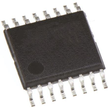
| 产品图片 |
|
| rohs | 符合RoHS无铅 / 符合限制有害物质指令(RoHS)规范要求 |
| 产品系列 | 接口 IC,RS-232接口集成电路,Analog Devices ADM3202ARUZ- |
| 数据手册 | |
| 产品型号 | ADM3202ARUZ |
| 产品目录页面 | |
| 产品种类 | RS-232接口集成电路 |
| 供应商器件封装 | 16-TSSOP |
| 关闭 | No |
| 功能 | Transceiver |
| 包装 | 管件 |
| 协议 | RS232 |
| 双工 | 全 |
| 商标 | Analog Devices |
| 安装类型 | 表面贴装 |
| 安装风格 | SMD/SMT |
| 封装 | Tube |
| 封装/外壳 | 16-TSSOP(0.173",4.40mm 宽) |
| 封装/箱体 | TSSOP-16 |
| 工作温度 | -40°C ~ 85°C |
| 工作温度范围 | - 40 C to + 85 C |
| 工作电源电压 | 3 V to 5.5 V |
| 工厂包装数量 | 96 |
| 接收器滞后 | 400mV |
| 接收机数量 | 2 Receiver |
| 支持协议 | RS-232 |
| 数据速率 | 460Kbps |
| 最大工作温度 | + 85 C |
| 最小工作温度 | - 40 C |
| 标准包装 | 96 |
| 激励器数量 | 2 Driver |
| 电压-电源 | 3 V ~ 5.5 V |
| 电源电流 | 3 mA |
| 类型 | 收发器 |
| 系列 | ADM3202 |
| 驱动器/接收器数 | 2/2 |


PDF Datasheet 数据手册内容提取
Low Power, 3.3 V, RS-232 Line Drivers/Receivers ADM3202/ADM3222/ADM1385 FEATURES FUNCTIONAL BLOCK DIAGRAMS 460 kbps data rate +3.3VINPUT Specified at 3.3 V Meets EIA-232E specifications 0.110µVF+ CC11+– +3.DV3OOVULTTBOALG+E6ER.6VVVCC+ +C0.31µF +C0.51µF 0.1 μF charge pump capacitors 0.1µF+ C2++6.V6OVLTTOAG–6E.6V V– 6C.43V Low power shutdown (ADM3222 and ADM1385) 10V C2– INVERTER +0.1µF 10V PDIP, SOIC_N, SOIC_W, SSOP, and TSSOP options Upgrade for MAX3222/MAX3232 and LTC1385 CMOS T1IN T1 T1OUT EIA/TIA-232 INPUTS OUTPUTS ESD protection to IEC 1000-4-2 (801.2) T2IN T2 T2OUT on RS-232 pins (ADM3202 only) CMOS R1OUT R1 R1IN EIA/TIA-232 ±8 kV: contact discharge OUTPUTS INPUTS* R2OUT R2 R2IN ±15 kV: air gap discharge GND ADM3202 APPLICATIONS * OINNTEERANCAHLR5Sk-Ω23P2 UINLPLU-DTOWNRESISTOR 00071-001 Figure 1. General-purpose RS-232 data link +3.3VINPUT Portable instruments Printers, palmtop computers, PDAs 0.110µVF+ CC11+– +3.DV3OOVULTTBOALG+E6ER.6VVVCC+ +C0.31µF +C0.51µF 6.3V GENERAL DESCRIPTION 0.110µVF+ CC22+– +6I.VN6OVVLETTROATG–E6ER.6V V– +C0.41µF 10V The ADM3202/ADM3222/ADM1385 transceivers are high CMOS T1IN T1 T1OUT EIA/TIA-232 speed, 2-channel RS-232/V.28 interface devices that operate INPUTS OUTPUTS from a single 3.3 V power supply. Low power consumption and T2IN T2 T2OUT a shutdown facility (ADM3222/ADM1385) make them ideal for CMOS R1OUT R1 R1IN EIA/TIA-232 battery-powered portable instruments. OUTPUTS R2OUT R2 R2IN INPUTS* The ADM3202/ADM3222/ADM1385 parts conform to the EN SD EIA-232E and CCITT V.28 specifications and operate at data GND ADM3222 rates up to 460 kbps. * OINNTEERANCAHLR5Sk-Ω23P2 UINLPLU-DTOWNRESISTOR 00071-002 Four external 0.1 μF charge pump capacitors are used for the Figure 2. voltage doubler/inverter, permitting operation from a single +3.3V INPUT 3.3 V supply. The ADM3222 contains additional enable and shutdown 0.110µVF+ CC11+–+3.DV3OOVULTTBOAL G+E6ER.6VVVCC+ +C3 +C0.51µF circuitry. The EN input can be used to three-state the receiver 0.1µF outputs. The SD input is used to power down the charge pump 0.110µVF+ CC22+– +6I.VN6OVVLETTROAT G–E6ER.6V V– +C0.41µF 10V 10V and transmitter outputs, reducing the quiescent current to less than 0.5 μA. The receivers remain enabled during shutdown CMOS T1IN T1 T1OUT EIA/TIA-232 INPUTS OUTPUTS unless disabled using EN. T2IN T2 T2OUT The ADM1385 contains a driver disable mode and a complete CMOS R1OUT R1 R1IN EIA/TIA-232 OUTPUTS INPUTS* shutdown mode. R2OUT R2 R2IN The ADM3202 is available in a 16-lead PDIP, SOIC_W, and DD SD SOIC_N, as well as a space-saving 16-lead TSSOP. The ADM3222 GND ADM1385 iasn adv TaiSlaSbOleP .i nT h18e -AleDadM P1D38IP5 iasn adv aSiOlaIbCle_ Win aa n2d0 -ilne a2d0 -SlSeOadP ,S SOP * OINNT EERANCAHL R 5Sk-Ω23 P2 UINLPLU-DTOWN RESISTOR 00071-003 Figure 3. which is pin-compatible with the LTC1385 CG. Rev. E Information furnished by Analog Devices is believed to be accurate and reliable. However, no responsibility is assumed by Analog Devices for its use, nor for any infringements of patents or other One Technology Way, P.O. Box 9106, Norwood, MA 02062-9106, U.S.A. rights of third parties that may result from its use. Specifications subject to change without notice. No license is granted by implication or otherwise under any patent or patent rights of Analog Devices. Tel: 781.329.4700 www.analog.com Trademarks and registered trademarks are the property of their respective owners. Fax: 781.461.3113 ©1998–2011 Analog Devices, Inc. All rights reserved.
ADM3202/ADM3222/ADM1385 TABLE OF CONTENTS Features..............................................................................................1 Pin Configurations (N, RN, RU, and RW Packages)................5 Applications.......................................................................................1 Pin Configurations (RS and RU Packages)................................5 General Description.........................................................................1 Typical Performance Characteristics..............................................6 Functional Block Diagrams.............................................................1 General Description..........................................................................8 Revision History...............................................................................2 Circuit Description.......................................................................8 Specifications.....................................................................................3 High Baud Rate..............................................................................9 Absolute Maximum Ratings............................................................4 Outline Dimensions.......................................................................10 ESD Caution..................................................................................4 Ordering Guide..........................................................................14 Pin Configurations and Function Descriptions...........................5 REVISION HISTORY 7/11—Rev. D to Rev. E Changes to Figure 3..........................................................................1 Changes to Table 2............................................................................4 Changes to Figure 17........................................................................8 Updated Outline Dimensions.......................................................10 Changes to Ordering Guide..........................................................14 8/06—Rev. C to Rev. D Changes to Table 1............................................................................3 Updated Outline Dimensions.......................................................10 Changes to Ordering Guide..........................................................12 9/05—Rev. B to Rev. C Updated Outline Dimensions.......................................................10 Changes to Ordering Guide..........................................................12 12/01—Rev. A to Rev. B Changes to Specifications Page.......................................................2 Rev. E | Page 2 of 16
ADM3202/ADM3222/ADM1385 SPECIFICATIONS V = 3.3 V ± 0.3 V, C1 to C4 = 0.1 μF. All specifications T to T , unless otherwise noted. CC MIN MAX Table 1. Parameter Min Typ Max Unit Test Conditions/Comments DC CHARACTERISTICS Operating Voltage Range 3.0 3.3 5.5 V V Power Supply Current 1.3 3 mA No load CC 8 12 mA R = 3 kΩ to GND L Shutdown Supply Current 0.01 0.5 μA LOGIC Input Logic Threshold Low, V 0.8 V T INL IN Input Logic Threshold High, V 2.0 V T INH IN CMOS Output Voltage Low, V 0.4 V I = 1.6 mA OL OUT CMOS Output Voltage High, V V − 0.6 V I = −1 mA OH CC OUT Logic Pull-Up Current 5 10 μA T = GND to V 1 IN CC Output Leakage Current ±10 μA Receivers disabled RS-232 RECEIVER EIA-232 Input Voltage Range −30 +30 V EIA-232 Input Threshold Low 0.6 1.2 V EIA-232 Input Threshold High 1.6 2.4 V EIA-232 Input Hysteresis 0.4 V EIA-232 Input Resistance 3 5 7 kΩ RS-232 TRANSMITTER Output Voltage Swing (RS-232) ±5.0 ±5.2 V V = 3.3 V, all transmitter outputs loaded with 3 kΩ to ground CC Output Voltage Swing (RS-562) ±3.7 V V = 3.0 V CC Transmitter Output Resistance 300 Ω V = 0 V, V = ±2 V CC OUT RS-232 Output Short-Circuit Current ±15 mA Output Leakage Current ±25 μA SD = low, V = 12 V OUT TIMING CHARACTERISTICS Maximum Data Rate 460 kbps V = 3.3 V, R = 3 kΩ to 7 kΩ, C = 50 pF to 1000 pF, one CC L L Tx switching Receiver Propagation Delay TPHL 0.4 1 μs TPLH 0.4 1 μs Transmitter Propagation Delay 0.3 1.2 μs R = 3 kΩ, C = 1000 pF L L Receiver Output Enable Time 200 ns Receiver Output Disable Time 200 ns Transmitter Skew 30 ns Receiver Skew 300 ns Transition Region Slew Rate 5.5 10 30 V/μs Measured from +3 V to −3 V or −3 V to +3 V, V = +3.3 V; CC R = 3 kΩ, C = 1000 pF, T = 25°C L L A 1 ADM1385: Input leakage current typically −10 μA when TIN = GND. Rev. E | Page 3 of 16
ADM3202/ADM3222/ADM1385 ABSOLUTE MAXIMUM RATINGS T = 25°C, unless otherwise noted. A Stresses above those listed under Absolute Maximum Ratings Table 2. may cause permanent damage to the device. This is a stress Parameter Rating rating only; functional operation of the device at these or any V −0.3 V to +6 V CC other conditions above those indicated in the operational V+ (V − 0.3 V) to +14 V CC section of this specification is not implied. Exposure to absolute V− +0.3 V to –14 V maximum rating conditions for extended periods may affect Input Voltages device reliability. T −0.3 V to (V+, +0.3 V) IN RIN ±30 V ESD CAUTION Output Voltages T ±15 V OUT R −0.3 V to (V + 0.3 V) OUT CC Short-Circuit Duration T Continuous OUT Power Dissipation (Derates 6 mW/°C 450 mW above 50°C) Thermal Impedance, θ JA N-16/N-18 (2-Layer Test Board) 117°C/W RW-16/RW-18 (4-Layer Test Board) 56°C/W R-16 (4-Layer Test Board) 81°C/W RU-16 (4-Layer Test Board) 113°C/W RU-20 (4-Layer Test Board) 110°C/W RS-20 (4-Layer Test Board) 83°C/W Operating Temperature Range Industrial (A Version) −40°C to +85°C Storage Temperature Range −65°C to +150°C Lead Temperature JEDEC industry (Soldering, 10 sec) standard J-STD-020 Rev. E | Page 4 of 16
ADM3202/ADM3222/ADM1385 PIN CONFIGURATIONS AND FUNCTION DESCRIPTIONS PIN CONFIGURATIONS (N, R, RU, AND RW PACKAGES) C1+ 1 16 VCC EN 1 18 SD V+ 2 15 GND C1+ 2 17 VCC ADM3202 V+ 3 ADM3222 16 GND C1– 3 14 T1OUT TOP VIEW C1– 4 TOP VIEW 15 T1OUT C2+ 4 (Not to Scale) 13 R1IN C2+ 5 (Not to Scale) 14 R1IN C2– 5 12 R1OUT C2– 6 13 R1OUT V– 6 11 T1IN V– 7 12 T1IN T2RO2UINT 78 190 TR22IONUT00071-004 T2RO2UINT 89 1110 TR22IONUT00071-005 Figure 4. N, R, RU, and RW Packages Pin Configuration Figure 5. N and RW Packages Pin Configuration PIN CONFIGURATIONS (RS AND RU PACKAGES) EN 1 20 SD DD 1 20 SD C1+ 2 19 VCC CV1++ 23 ADM1385 1189 VGCNCD V+ 3 ADM3222 18 GND C1– 4 (SSOP) 17 T1OUT C1– 4 (SSOP/TSSOP) 17 T1OUT C2+ 5 TOP VIEW 16 R1IN C2+ 5 (NToOt Pto V SIEcWale) 16 R1IN CV2–– 67 (Not to Scale) 1154 RT11IONUT C2– 6 15 R1OUT T2OUT 8 13 T2IN V– 7 14 NC R2IN 9 12 R2OUT T2RO2UINT 89 1132 TT21IINN NC 10NC = NO CONNECT11 NC 00071-007 R2OUT 10NC = NO CONNECT11 NC 00071-006 Figure 6. RS and RU Packages Pin Configuration Figure 7. RS Package Pin Configuration Table 3. Pin Function Descriptions Mnemonic Description V Power Supply Input (3.3 V ± 0.3 V). CC V+ Internally Generated Positive Supply (+6 V nominal). V– Internally Generated Negative Supply (−6 V nominal). GND Ground Pin. Must be connected to 0 V. C1+, C1– External Capacitor 1 is connected between these pins. A 0.1 μF capacitor is recommended but larger capacitors up to 47 μF can be used. C2+, C2– External Capacitor 2 is connected between these pins. A 0.1 μF capacitor is recommended but larger capacitors up to 47 μF can be used. Tx Transmitter (Driver) Inputs. These inputs accept TTL/CMOS levels. IN Tx Transmitter (Driver) Outputs. These are RS-232 signal levels (typically ±9 V). OUT Rx Receiver Inputs. These inputs accept RS-232 signal levels. An internal 5 kΩ pull-down resistor to GND is connected on each input. IN Rx Receiver Outputs. These are CMOS output logic levels. OUT EN (ADM3222 only) Receiver Enable. Active low. When low, the receiver outputs are enabled. When high, they are three-stated. SD (ADM3222 only) Shutdown Control. Active low. When low, the charge pump is shut down and the transmitter outputs are disabled. SD (ADM1385 only) Shutdown Control. When low, the charge pump is shut down and all transmitters and receivers are disabled. DD (ADM1385 only) Driver Disable. When low, the charge pump is turned off and the transmitters are disabled. The receivers remain active. NC No Connect. Rev. E | Page 5 of 16
ADM3202/ADM3222/ADM1385 TYPICAL PERFORMANCE CHARACTERISTICS 8 8 TOUT (HIGH) 6 6 V+ 4 4 V) E ( 2 2 VOLTAG 0 +, V– (V) 0 P V O/ –2 –2 x T –4 –4 V– ––86 TOUT (LOW) 00071-008 ––86 00071-011 0 200 400 600 800 1000 1200 0 2 4 6 8 10 12 LOAD CAPACITANCE (pF) LOAD CURRENT (mA) Figure 8. Transmitter Output Voltage High/Low vs. Figure 11. Charge Pump V+, V− vs. Load Current Load Capacitance @ 460 kbps 8 350 Tx O/P HIGH 6 300 V+(IMPEDANCE) 4 250 2 Ω) x O/P (V) 0 EDANCE (210500 V–(IMPEDANCE) T P –2 M I 100 –4 Tx O/P LOW 50 ––68 00071-009 0 00071-012 2.7 2.9 3.1 3.3 3.5 2.7 2.9 3.1 3.3 3.5 VCC (V) VCC(V) Figure 9. Transmitter Output Voltage vs. VCC Figure 12. Charge Pump Impedance vs. VCC 8 20 18 6 Tx O/P HIGH ICC @ 460kbps 16 4 14 2 x O/P (V) 0 (mA)CC1120 ICC @ 230kbps T I 8 –2 6 –4 Tx O/P LOW 4 ––68 00071-010 20 00071-013 0 2 4 6 8 10 12 0 1000 2000 3000 LOAD CURRENT (mA) LOAD CAPACITANCE (pF) Figure 10. Transmitter Output Voltage Low/High vs. Load Current Figure 13. Power Supply Current vs. Load Capacitance Rev. E | Page 6 of 16
ADM3202/ADM3222/ADM1385 1 T T 2 CH1 5.00V CH2 5.00V M1.00µs CH1 0V 00071-014 Figure 14. 460 kbps Data Transmission Rev. E | Page 7 of 16
ADM3202/ADM3222/ADM1385 GENERAL DESCRIPTION The ADM3202/ADM3222/ADM1385 are RS-232 line drivers/ +3.3V INPUT rtreacneisvmeritst.e Srtse apn-udp r evcoelitvaegres caollnovwe rRteSr-s2 c3o2u lpevleedls w toit hb el edveevl-eslhopifetidn g 0.110µVF+ CC11+– +3.DV3OOVULTTBOALG+E6ER.6VVVCC+ +C0.31µF +C0.51µF 6.3V while operating from a single 3.3 V supply. 0.1µF+ C2++6.V6OVLTTOAG–6E.6V V– C4 10V C2– INVERTER +0.1µF 10V CMOS technology is used to keep the power dissipation to an absolute minimum, allowing maximum battery life in portable CMOS T1IN T1 T1OUT EIA/TIA-232 INPUTS OUTPUTS applications. T2IN T2 T2OUT The ADM3202/ADM3222/ADM1385 are modifications, CMOS R1OUT R1 R1IN EIA/TIA-232 OUTPUTS INPUTS* enhancements, and improvements of the AD230 to AD241 R2OUT R2 R2IN family and derivatives. They are essentially plug-in compatible EN SD and do not have any materially different applications. GND ADM3222 CIRCUIT DESCRIPTION *OINNTEERANCAHLR5Sk-Ω23P2 UINLPLU-DTOWNRESISTOR 00071-016 Figure 16. ADM3222 Typical Operating Circuit The internal circuitry consists of these main sections: • A charge pump voltage converter +3.3V INPUT • 3.3 V logic to EIA-232 transmitters 0.110µVF+ CC11+–+3.DV3OOVULTTBOAL G+E6ER.6VVVCC+ +C3 +C0.51µF • EIA-232 to 5 V logic receivers 0.1µF 0.1µF+ C2++6.V6OVLTTOA G–6E.6V V– C4 10V 10V C2– INVERTER +0.1µF Charge Pump DC to DC Voltage Converter 10V The charge pump voltage converter consists of a 200 kHz CMOS T1IN T1 T1OUT EIA/TIA-232 INPUTS OUTPUTS oscillator and a switching matrix. The converter generates a T2IN T2 T2OUT ±6.6 V supply from the input 3.3 V level. This is done in two CMOS R1OUT R1 R1IN EIA/TIA-232 stages by using a switched capacitor technique as illustrated in OUTPUTS INPUTS* R2OUT R2 R2IN Figure 18 and Figure 19. First, the 3.3 V input supply is doubled to 6.6 V by using Capacitor C1 as the charge storage element. DD SD GND ADM1385 Tash teh +e 6s.t6o rVag lee veelel mis etnhte.n C i3n vise rstheodw ton gceonnenreacttee −d6 b.6et Vw euesnin Vg+ C a2n d * OINNT EERANCAHL R 5Sk-Ω23 P2 UINLPLU-DTOWN RESISTOR 00071-017 VCC but is equally effective if connected between V+ and GND. Figure 17. ADM1385 Typical Operating Circuit Capacitors C3 and C4 are used to reduce the output ripple. S1 S3 Their values are not critical and can be increased, if desired. VCC V+ = 2VCC Capacitor C3 is shown connected between V+ and V . It is + + CC C1 C3 also acceptable to connect this capacitor between V+ and GND. S2 S4 GND VCC ICf adpeasciriteodr,s l aCr1g etro cCa4p.a citors (up to 10 μF) can be used for OISNCTIELRLANTAOLR 00071-018 Figure 18. Charge Pump Voltage Doubler +3.3V INPUT 00..111100µµVVFF++ CCCC1212++–– ++36I.D.VVN36OOOVVVULLETTTTBROOAALTGG+–EE66EERR..66VVVVVCC+– ++C06C0...34131µVµFF +C0.51µF DVOOULFTBRALOGEMRE V+ SS21 C2 + SS43 C4 + GND 10V GND V– =–(V+) INCPMUOTSS TT12IINN T1 T2 TT12OOUUTT EOIUAT/TPIUAT-2S32 OISNCTIELRLANTAOLR 00071-019 Figure 19. Charge Pump Voltage Inverter CMOS R1OUT R1 R1IN EIA/TIA-232 OUTPUTS INPUTS* R2OUT R2 R2IN GND ADM3202 *OINNTEERANCAHLR5Sk-Ω23P2 UINLPLU-DTOWNRESISTOR 00071-015 Figure 15. ADM3202 Typical Operating Circuit Rev. E | Page 8 of 16
ADM3202/ADM3222/ADM1385 Transmitter (Driver) Section HIGH BAUD RATE The drivers convert 3.3 V logic input levels into RS-232 output The ADM3202/ADM3222 feature high slew rates permitting levels. With VCC = 3.3 V and driving an RS-232 load, the output data transmission at rates well in excess of the EIA/RS-232E voltage swing is typically ±6 V. specifications. RS-232 voltage levels are maintained at data rates up to 460 kbps even under worst-case loading conditions. This Receiver Section allows high speed data links between two terminals and is The receivers are inverting level-shifters that accept RS-232 suitable for the new generation ISDN modem standards that input levels and translate them into 3 V logic output levels. The require data rates of 230 kbps. The slew rate is internally inputs have internal 5 kΩ, pull-down resistors to ground and are controlled to less than 30 V/μs to minimize EMI interference. protected against overvoltages up to ±30 V. Unconnected inputs are pulled to 0 V by the internal 5 kΩ, pull-down resistor. This results in a Logic 1 output level for unconnected inputs or for inputs connected to GND. The receivers have Schmitt-trigger inputs with a hysteresis level of 0.4 V. This ensures error-free reception for both noisy inputs and for inputs with slow transition times. Rev. E | Page 9 of 16
ADM3202/ADM3222/ADM1385 OUTLINE DIMENSIONS 0.800 (20.32) 0.790 (20.07) 0.780 (19.81) 16 9 0.280 (7.11) 0.250 (6.35) 1 8 0.240 (6.10) 0.325 (8.26) 0.310 (7.87) 0.100 (2.54) 0.300 (7.62) BSC 0.060 (1.52) 0.195 (4.95) 0.210 (5.33) MAX 0.130 (3.30) MAX 0.115 (2.92) 0.015 0.150 (3.81) (0.38) 0.015 (0.38) 0.130 (3.30) MIN GAUGE 0.115 (2.92) SEATING PLANE 0.014 (0.36) PLANE 0.010 (0.25) 0.022 (0.56) 0.008 (0.20) 0.005 (0.13) 0.430 (10.92) 0.018 (0.46) MIN MAX 0.014 (0.36) 0.070 (1.78) 0.060 (1.52) 0.045 (1.14) COMPLIANTTO JEDEC STANDARDS MS-001-AB CONTROLLING DIMENSIONSARE IN INCHES; MILLIMETER DIMENSIONS (RCINOEFRPEANRREERENN LCTEEHA EODSNSEL MSY)AAAYNR BDEE AR CROOEU NNNFODIGETUDAR-POEPFDRFOA INSPC RWHIAH ETOEQL UFEIO VORAR LU EHSNAETL ISFN FLDOEEARSDIGSN.. 073106-B Figure 20. 16-Lead Plastic Dual In-Line Package [PDIP] Narrow Body (N-16) Dimensions shown in inches and (millimeters) 10.00 (0.3937) 9.80 (0.3858) 4.00 (0.1575) 16 9 6.20 (0.2441) 3.80 (0.1496) 1 8 5.80 (0.2283) 1.27 (0.0500) 0.50 (0.0197) BSC 1.75 (0.0689) 0.25 (0.0098) 45° 0.25 (0.0098) 1.35 (0.0531) 8° 0.10 (0.0039) 0° COPLANARITY SEATING 0.10 0.51 (0.0201) PLANE 0.25 (0.0098) 1.27 (0.0500) 0.31 (0.0122) 0.17 (0.0067) 0.40 (0.0157) COMPLIANTTO JEDEC STANDARDS MS-012-AC C(RINOEFNPEATRRREOENNLCLTEIHN EOGSN EDLSIYM)AEANNRDSEI AORRNOESU NANORDEET DAIN-PO MPFRIFLO LMPIIMRLELIATIMTEEER TFSEO; RIRN ECUQHSU EDI VIINMA LEDENENSSTIIOGSN NFS.OR 060606-A Figure 21. 16-Lead Standard Small Outline Package [SOIC_N] Narrow Body (R-16) Dimensions shown in millimeters and (inches) Rev. E | Page 10 of 16
ADM3202/ADM3222/ADM1385 5.10 5.00 4.90 16 9 4.50 6.40 4.40 BSC 4.30 1 8 PIN 1 1.20 MAX 0.15 0.20 0.05 0.09 0.75 0.30 8° 0.60 B0S.6C5 0.19 SEATING 0° 0.45 PLANE COPLANARITY 0.10 COMPLIANT TO JEDEC STANDARDS MO-153-AB Figure 22. 16-Lead Thin Shrink Small Outline Package [TSSOP] (RU-16) Dimensions shown in millimeters 10.50(0.4134) 10.10(0.3976) 16 9 7.60(0.2992) 7.40(0.2913) 1 10.65(0.4193) 8 10.00(0.3937) 1.27(0.0500) 0.75(0.0295) BSC 2.65(0.1043) 0.25(0.0098) 45° 0.30(0.0118) 2.35(0.0925) 8° 0.10(0.0039) 0° COPLANARITY 0.10 0.51(0.0201) SPLEAATNIENG 0.33(0.0130) 1.27(0.0500) 0.31(0.0122) 0.20(0.0079) 0.40(0.0157) C(RINOEFNPEATRRREOENNLCLTEIHNCEOGOSNDMELISPYM)LAEAIANNRNDSETIAORTRNOOESUJNANEORDDETEEDAICN-POSMPFTRIFALONLMPIDMIRLAELIRATIMTDEEESRTFSMEO;SRIRN-0ECU1QH3SU-EADIVAIINMAELDENENSSTIIOGSNNFS.OR 03-27-2007-B Figure 23. 16-Lead Standard Small Outline Package [SOIC_W] Wide Body (RW-16) Dimensions shown in millimeters and (inches) Rev. E | Page 11 of 16
ADM3202/ADM3222/ADM1385 0.920 (23.37) 0.900 (22.86) 0.880 (22.35) 18 10 0.280 (7.11) 0.250 (6.35) 1 9 0.240 (6.10) 0.325 (8.26) 0.310 (7.87) 0.100 (2.54) 0.300 (7.62) BSC 0.060 (1.52) 0.195 (4.95) 0.210 (5.33) MAX 0.130 (3.30) MAX 0.115 (2.92) 0.015 0.150 (3.81) (0.38) 0.015 (0.38) 0.130 (3.30) MIN GAUGE 0.115 (2.92) SEATING PLANE 0.014 (0.36) PLANE 0.010 (0.25) 0.022 (0.56) 0.008 (0.20) 0.005 (0.13) 0.430 (10.92) 0.018 (0.46) MIN MAX 0.014 (0.36) 0.070 (1.78) 0.060 (1.52) 0.045 (1.14) COMPLIANTTO JEDEC STANDARDS MS-001 CONTROLLING DIMENSIONSARE IN INCHES; MILLIMETER DIMENSIONS (RCINOEFRPEANRREEREN NLCTEEHA EODSNSEL MSY)AAAYNR BDEE AR CROOEU NNNFODIGETUDAR-POEPFDRFOA INSPC RWHIAH ETOEQL UFEIO VORAR LU EHSNAETL ISFN FLDOEEARSDIGSN.. 070706-A Figure 24. 18-Lead Plastic Dual In-Line Package [PDIP] Narrow Body (N-18) Dimensions shown in inches and (millimeters) 7.50 7.20 6.90 20 11 5.60 5.30 5.00 8.20 7.80 1 7.40 10 1.85 0.25 2.00 MAX 1.75 0.09 1.65 COPLA0N.0A5R MITIYN 0.65 BSC 00..3282 SPLEAATNIENG 840°°° 000...975555 0.10 COMPLIANTTO JEDEC STANDARDS MO-150-AE 060106-A Figure 25. 20-Lead Shrink Small Outline Package [SSOP] (RS-20) Dimensions shown in millimeters Rev. E | Page 12 of 16
ADM3202/ADM3222/ADM1385 6.60 6.50 6.40 20 11 4.50 4.40 4.30 6.40 BSC 1 10 PIN 1 0.65 BSC 0.15 1.20 MAX 0.20 0.05 0.09 0.75 0.30 8° 0.60 COPLANARITY 0.19 SEATING 0° 0.45 0.10 PLANE COMPLIANT TO JEDEC STANDARDS MO-153-AC Figure 26. 20-Lead Thin Shrink Small Outline Package [TSSOP] (RU-20) Dimensions shown in millimeters 11.75 (0.4626) 11.35 (0.4469) 18 10 7.60 (0.2992) 7.40 (0.2913) 1 10.65 (0.4193) 9 10.00 (0.3937) 0.75 (0.0295) 45° 2.65 (0.1043) 0.25 (0.0098) 0.30 (0.0118) 2.35 (0.0925) 8° 0.10 (0.0039) 0° COPLANARITY 0.10 (0.10.52070) 00..5311 ((00..00210212)) SPLEAATNIENG 00..3230 ((00..00103709)) 10..2470 ((00..00510507)) BSC COMPLIANTTO JEDEC STANDARDS MS-013-AB C(RINOEFNPEATRRREOENNLCLTEIHN EOGSN EDLSIYM)AEANNRDSEI AORRNOESU NANORDEET DAIN-PO MPFRIFLO LMPIIMRLELIATIMTEEER TFSEO; RIRN ECUQHSU EDI VIINMA LEDENENSSTIIOGSN NFS.OR 060706-A Figure 27. 18-Lead Standard Small Outline Package [SOIC_W] Wide Body (RW-18) Dimensions shown in millimeters and (inches) Rev. E | Page 13 of 16
ADM3202/ADM3222/ADM1385 ORDERING GUIDE Model1 Temperature Range Package Description Package Option ADM3202AN −40°C to +85°C 16-Lead Plastic Dual In-Line Package [PDIP] N-16 ADM3202ANZ −40°C to +85°C 16-Lead Plastic Dual In-Line Package [PDIP] N-16 ADM3202ARN −40°C to +85°C 16-Lead Standard Small Outline Package [SOIC_N] R-16 ADM3202ARN-REEL −40°C to +85°C 16-Lead Standard Small Outline Package [SOIC_N] R-16 ADM3202ARN-REEL7 −40°C to +85°C 16-Lead Standard Small Outline Package [SOIC_N] R-16 ADM3202ARNZ −40°C to +85°C 16-Lead Standard Small Outline Package [SOIC_N] R-16 ADM3202ARNZ-REEL −40°C to +85°C 16-Lead Standard Small Outline Package [SOIC_N] R-16 ADM3202ARNZ-REEL7 −40°C to +85°C 16-Lead Standard Small Outline Package [SOIC_N] R-16 ADM3202ARU −40°C to +85°C 16-Lead Thin Shrink Small Outline Package [TSSOP] RU-16 ADM3202ARU-REEL −40°C to +85°C 16-Lead Thin Shrink Small Outline Package [TSSOP] RU-16 ADM3202ARU-REEL7 −40°C to +85°C 16-Lead Thin Shrink Small Outline Package [TSSOP] RU-16 ADM3202ARUZ −40°C to +85°C 16-Lead Thin Shrink Small Outline Package [TSSOP] RU-16 ADM3202ARUZ-REEL −40°C to +85°C 16-Lead Thin Shrink Small Outline Package [TSSOP] RU-16 ADM3202ARUZ-REEL7 −40°C to +85°C 16-Lead Thin Shrink Small Outline Package [TSSOP] RU-16 ADM3202ARW −40°C to +85°C 16-Lead Standard Small Outline Package [SOIC_W] RW-16 ADM3202ARW-REEL7 −40°C to +85°C 16-Lead Standard Small Outline Package [SOIC_W] RW-16 ADM3202ARWZ −40°C to +85°C 16-Lead Standard Small Outline Package [SOIC_W] RW-16 ADM3202ARWZ-REEL −40°C to +85°C 16-Lead Standard Small Outline Package [SOIC_W] RW-16 ADM3202ARWZ-REEL7 −40°C to +85°C 16-Lead Standard Small Outline Package [SOIC_W] RW-16 ADM3222AN −40°C to +85°C 18-Lead Plastic Dual In-Line Package [PDIP] N-18 ADM3222ANZ −40°C to +85°C 18-Lead Plastic Dual In-Line Package [PDIP] N-18 ADM3222ARS −40°C to +85°C 20-Lead Shrink Small Outline Package [SSOP] RS-20 ADM3222ARS-REEL −40°C to +85°C 20-Lead Shrink Small Outline Package [SSOP] RS-20 ADM3222ARS-REEL7 −40°C to +85°C 20-Lead Shrink Small Outline Package [SSOP] RS-20 ADM3222ARSZ −40°C to +85°C 20-Lead Shrink Small Outline Package [SSOP] RS-20 ADM3222ARSZ-REEL −40°C to +85°C 20-Lead Shrink Small Outline Package [SSOP] RS-20 ADM3222ARSZ-REEL7 −40°C to +85°C 20-Lead Shrink Small Outline Package [SSOP] RS-20 ADM3222ARU −40°C to +85°C 20-Lead Thin Shrink Small Outline Package [TSSOP] RU-20 ADM3222ARU-REEL −40°C to +85°C 20-Lead Thin Shrink Small Outline Package [TSSOP] RU-20 ADM3222ARU-REEL7 −40°C to +85°C 20-Lead Thin Shrink Small Outline Package [TSSOP] RU-20 ADM3222ARUZ −40°C to +85°C 20-Lead Thin Shrink Small Outline Package [TSSOP] RU-20 ADM3222ARUZ-REEL −40°C to +85°C 20-Lead Thin Shrink Small Outline Package [TSSOP] RU-20 ADM3222ARUZ-REEL7 −40°C to +85°C 20-Lead Thin Shrink Small Outline Package [TSSOP] RU-20 ADM3222ARW −40°C to +85°C 18-Lead Standard Small Outline Package [SOIC_W] RW-18 ADM3222ARW-REEL −40°C to +85°C 18-Lead Standard Small Outline Package [SOIC_W] RW-18 ADM3222ARWZ −40°C to +85°C 18-Lead Standard Small Outline Package [SOIC_W] RW-18 ADM3222ARWZ-REEL −40°C to +85°C 18-Lead Standard Small Outline Package [SOIC_W] RW-18 ADM3222ARWZ-REEL7 −40°C to +85°C 18-Lead Standard Small Outline Package [SOIC_W] RW-18 ADM1385ARS −40°C to +85°C 20-Lead Shrink Small Outline Package [SSOP] RS-20 ADM1385ARSZ −40°C to +85°C 20-Lead Shrink Small Outline Package [SSOP] RS-20 ADM1385ARSZ-REEL −40°C to +85°C 20-Lead Shrink Small Outline Package [SSOP] RS-20 ADM1385ARSZ-REEL7 −40°C to +85°C 20-Lead Shrink Small Outline Package [SSOP] RS-20 1 Z = RoHS Compliant Part. Rev. E | Page 14 of 16
ADM3202/ADM3222/ADM1385 NOTES Rev. E | Page 15 of 16
ADM3202/ADM3222/ADM1385 NOTES ©1998–2011 Analog Devices, Inc. All rights reserved. Trademarks and registered trademarks are the property of their respective owners. D00071-0-7/11(E) Rev. E | Page 16 of 16
Mouser Electronics Authorized Distributor Click to View Pricing, Inventory, Delivery & Lifecycle Information: A nalog Devices Inc.: ADM3222ANZ ADM3222ARW ADM3202ARU-REEL7 ADM3202AN ADM3222ARUZ ADM1385ARS ADM3202ARUZ ADM3202ARN-REEL7 ADM3222ARS-REEL7 ADM3222ARW-REEL ADM3222ARU ADM3202ARW- REEL7 ADM1385ARSZ-REEL ADM3202ARU ADM3222ARS ADM3222AN ADM3222ARU-REEL7 ADM3202ARNZ- REEL ADM3202ARUZ-REEL ADM3202ARN-REEL ADM3222ARSZ ADM3222ARSZ-REEL7 ADM3222ARWZ-REEL ADM3202ARUZ-REEL7 ADM1385ARSZ ADM3222ARU-REEL ADM3202ARWZ ADM3202ARW ADM3202ARNZ- REEL7 ADM3222ARWZ-REEL7 ADM3222ARWZ ADM3202ARNZ ADM3202ARU-REEL ADM3202ARN ADM3202ANZ ADM3222ARS-REEL ADM3202ARWZ-REEL ADM3222ARSZ-REEL ADM3202ARWZ-REEL7 ADM3222ARUZ-REEL ADM1385ARSZ-REEL7 ADM3222ARUZ-REEL7