ICGOO在线商城 > CSD17311Q5
 Datasheet下载
- 型号: CSD17311Q5
- 制造商: Texas Instruments
- 库位|库存: xxxx|xxxx
- 要求:
| 数量阶梯 | 香港交货 | 国内含税 |
| +xxxx | $xxxx | ¥xxxx |
查看当月历史价格
查看今年历史价格
CSD17311Q5产品简介:
ICGOO电子元器件商城为您提供CSD17311Q5由Texas Instruments设计生产,在icgoo商城现货销售,并且可以通过原厂、代理商等渠道进行代购。 提供CSD17311Q5价格参考以及Texas InstrumentsCSD17311Q5封装/规格参数等产品信息。 你可以下载CSD17311Q5参考资料、Datasheet数据手册功能说明书, 资料中有CSD17311Q5详细功能的应用电路图电压和使用方法及教程。
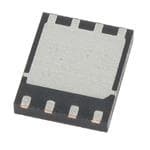
CSD17311Q5 是德州仪器(Texas Instruments)推出的单通道 N 沟道 NexFET™ 功率 MOSFET,采用 5mm × 6mm SON 封装,具有超低导通电阻(RDS(on) ≈ 1.8 mΩ @ VGS = 10 V)、快速开关特性及优异的热性能。其典型应用场景包括:

- 高效率 DC-DC 电源转换:广泛用于同步降压转换器(如 CPU/GPU 供电的 VRM、POL 模块),作为下管(low-side switch),配合控制器实现高电流(可达 30A+ 峰值)、高频率(1–2 MHz)下的高效功率输出。

- 电机驱动电路:适用于小型直流无刷电机(BLDC)或步进电机的 H 桥驱动中的功率开关,尤其在电池供电设备(如便携式工具、无人机电调)中兼顾效率与散热。

- 负载开关与热插拔保护:凭借低 RDS(on) 和集成 ESD 保护,常用于主板/模块的电源域隔离、USB PD 供电路径管理等场景,支持软启动与过流保护配合。

- LED 驱动与电源管理:在大电流 LED 恒流驱动或多相电源的相位控制中用作高速 PWM 开关。

该器件支持 3.3V/5V 逻辑电平驱动,具备雪崩耐受能力与强抗dv/dt干扰特性,适合空间受限、高功率密度的工业、通信和计算类应用。
| 参数 | 数值 |
| 产品目录 | |
| 描述 | MOSFET N-CH 30V 100A 8SONMOSFET 30V N-Channel NexFET Power MOSFET |
| 产品分类 | FET - 单分离式半导体 |
| FET功能 | 逻辑电平门 |
| FET类型 | MOSFET N 通道,金属氧化物 |
| Id-ContinuousDrainCurrent | 32 A |
| Id-连续漏极电流 | 32 A |
| 品牌 | Texas Instruments |
| 产品手册 | |
| 产品图片 |
|
| rohs | 符合RoHS含铅 / 不受限制有害物质指令(RoHS)规范要求限制 |
| 产品系列 | 晶体管,MOSFET,Texas Instruments CSD17311Q5NexFET™ |
| 数据手册 | |
| 产品型号 | CSD17311Q5 |
| PCN组件/产地 | |
| PCN设计/规格 | |
| Pd-PowerDissipation | 3.2 W |
| Pd-功率耗散 | 3.2 W |
| Qg-GateCharge | 24 nC |
| Qg-栅极电荷 | 24 nC |
| RdsOn-Drain-SourceResistance | 1.8 mOhms |
| RdsOn-漏源导通电阻 | 2.3 mOhms |
| Vds-Drain-SourceBreakdownVoltage | 30 V |
| Vds-漏源极击穿电压 | 30 V |
| Vgs-栅源极击穿电压 | 10 V |
| Vgsth-Gate-SourceThresholdVoltage | 1.2 V |
| Vgsth-栅源极阈值电压 | 1.2 V |
| 上升时间 | 18 ns |
| 下降时间 | 12 ns |
| 不同Id时的Vgs(th)(最大值) | 1.6V @ 250µA |
| 不同Vds时的输入电容(Ciss) | 4280pF @ 15V |
| 不同Vgs时的栅极电荷(Qg) | 31nC @ 4.5V |
| 不同 Id、Vgs时的 RdsOn(最大值) | 2 毫欧 @ 30A,8V |
| 产品培训模块 | http://www.digikey.cn/PTM/IndividualPTM.page?site=cn&lang=zhs&ptm=25585 |
| 产品种类 | MOSFET |
| 供应商器件封装 | 8-SON |
| 其它名称 | 296-27625-1 |
| 典型关闭延迟时间 | 33 ns |
| 制造商产品页 | http://www.ti.com/general/docs/suppproductinfo.tsp?distId=10&orderablePartNumber=CSD17311Q5 |
| 功率-最大值 | 3.2W |
| 包装 | 剪切带 (CT) |
| 商标 | Texas Instruments |
| 商标名 | NexFET |
| 安装类型 | 表面贴装 |
| 安装风格 | SMD/SMT |
| 封装 | Reel |
| 封装/外壳 | 8-TDFN 裸露焊盘 |
| 封装/箱体 | VSON-8 Clip |
| 工厂包装数量 | 2500 |
| 晶体管极性 | N-Channel |
| 最大工作温度 | + 150 C |
| 最小工作温度 | - 55 C |
| 标准包装 | 1 |
| 正向跨导-最小值 | 200 S |
| 漏源极电压(Vdss) | 30V |
| 电流-连续漏极(Id)(25°C时) | 32A(Ta), 100A(Tc) |
| 系列 | CSD17311Q5 |
| 视频文件 | http://www.digikey.cn/classic/video.aspx?PlayerID=1364138032001&width=640&height=455&videoID=541363338001http://www.digikey.cn/classic/video.aspx?PlayerID=1364138032001&width=640&height=455&videoID=1083957888001 |
| 设计资源 | http://www.digikey.com/product-highlights/cn/zh/texas-instruments-webench-design-center/3176 |
| 配置 | Single |


PDF Datasheet 数据手册内容提取
CSD17311Q5 www.ti.com SLPS257A–MARCH2010–REVISEDSEPTEMBER2010 30V N-Channel NexFET™ Power MOSFET CheckforSamples:CSD17311Q5 FEATURES PRODUCTSUMMARY 1 • Optimizedfor5VGateDrive VDS DraintoSourceVoltage 30 V 2 • UltraLowQ andQ Qg GateChargeTotal(4.5V) 24 nC g gd Qgd GateChargeGatetoDrain 5.2 nC • LowThermalResistance VGS=3V 2.3 mΩ • AvalancheRated RDS(on) DraintoSourceOnResistance VGS=4.5V 1.8 mΩ • PbFreeTerminalPlating VGS=8V 1.6 mΩ • RoHSCompliant VGS(th) ThresholdVoltage 1.2 V • HalogenFree ORDERINGINFORMATION • SON5-mm×6-mmPlasticPackage Device Package Media Qty Ship APPLICATIONS CSD17311Q5 SON5-mm×6-mm 13-Inch 2500 Tapeand PlasticPackage Reel Reel • NotebookPoint-of-Load • Point-of-LoadSynchronousBuckin ABSOLUTEMAXIMUMRATINGS Networking,TelecomandComputingSystems TA=25°Cunlessotherwisestated VALUE UNIT DESCRIPTION VDS DraintoSourceVoltage 30 V VGS GatetoSourceVoltage +10/–8 V The NexFET™ power MOSFET has been designed ContinuousDrainCurrent,TC=25°C 100 A to minimize losses in power conversion applications ID ContinuousDrainCurrent(1) 32 A andoptimizedfor5Vgatedriveapplications. IDM PulsedDrainCurrent,TA=25°C(2) 200 A TopView PD PowerDissipation(1) 3.2 W TJ, OperatingJunctionandStorage –55to150 °C TSTG TemperatureRange S 1 8 D AvalancheEnergy,SinglePulse EAS ID=113A,L=0.1mH,RG=25Ω 638 mJ S 2 7 D (1) Typical R = 40°C/W when mounted on a 1-inch2 qJA (6.45-cm2), 2-oz. (0.071-mm thick) Cu pad on a 0.06-inch S 3 6 D (1.52-mm)thickFR4PCB. D (2) Pulseduration≤300ms,dutycycle≤2%TextAddedForSpacing G 4 5 D Text_added_for_spacing_Text_added_for_spacing P0094-01 R vsV GATECHARGE DS(on) GS 6 8 Ωance - m 45 ID = 30A oltage - V 67 IVDD =S 3=0 1A5V sist TC = 125°C e V 5 e c e R 3 our 4 On-Stat 2 ate-to-S 3 - S(on) 1 TC = 25°C - GGS 2 RD V 1 0 0 0 1 2 3 4 5 6 7 8 9 10 0 5 10 15 20 25 30 35 40 VGS - Gate-to-Source Voltage - V G006 Qg - Gate Charge - nC G003 1 Pleasebeawarethatanimportantnoticeconcerningavailability,standardwarranty,anduseincriticalapplicationsofTexas Instrumentssemiconductorproductsanddisclaimerstheretoappearsattheendofthisdatasheet. NexFETisatrademarkofTexasInstruments. 2 PRODUCTIONDATAinformationiscurrentasofpublicationdate. Copyright©2010,TexasInstrumentsIncorporated Products conform to specifications per the terms of the Texas Instruments standard warranty. Production processing does not necessarilyincludetestingofallparameters.
CSD17311Q5 SLPS257A–MARCH2010–REVISEDSEPTEMBER2010 www.ti.com Thesedeviceshavelimitedbuilt-inESDprotection.Theleadsshouldbeshortedtogetherorthedeviceplacedinconductivefoam duringstorageorhandlingtopreventelectrostaticdamagetotheMOSgates. ELECTRICAL CHARACTERISTICS (T =25°Cunlessotherwisestated) A PARAMETER TESTCONDITIONS MIN TYP MAX UNIT StaticCharacteristics BV DraintoSourceVoltage V =0V,I =250mA 30 V DSS GS D I DraintoSourceLeakageCurrent V =0V,V =24V 1 mA DSS GS DS I GatetoSourceLeakageCurrent V =0V,V =+10/–8V 100 nA GSS DS GS V GatetoSourceThresholdVoltage V =V ,I =250mA 0.9 1.2 1.6 V GS(th) DS GS D V =3V,I =30A 2.3 3.1 mΩ GS D R DraintoSourceOnResistance V =4.5V,I =30A 1.8 2.3 mΩ DS(on) GS D V =8V,I =30A 1.6 2 mΩ GS D g Transconductance V =15V,I =30A 200 S fs DS D DynamicCharacteristics C InputCapacitance 3290 4280 pF iss V =0V,V =15V, C OutputCapacitance GS DS 1740 2260 pF oss f=1MHz C ReverseTransferCapacitance 85 110 pF rss R SeriesGateResistance 1.2 2.4 Ω G Q GateChargeTotal(4.5V) 24 31 nC g Qgd GateChargeGatetoDrain VDS=15V, 5.2 nC Qgs GateChargeGatetoSource IDS=30A 6.6 nC Q GateChargeatVth 3.9 nC g(th) Q OutputCharge V =14.8V,V =0V 47 nC oss DS GS t TurnOnDelayTime 12 ns d(on) tr RiseTime VDS=15V,VGS=4.5V, 18 ns td(off) TurnOffDelayTime IDS=30A,RG=2Ω 33 ns t FallTime 12 ns f DiodeCharacteristics V DiodeForwardVoltage I =30A,V =0V 0.85 1 V SD SD GS Qrr ReverseRecoveryCharge VDD=14.8V,IF=30A, 74 nC t ReverseRecoveryTime di/dt=300A/ms 39 ns rr THERMAL CHARACTERISTICS (T =25°Cunlessotherwisestated) A PARAMETER MIN TYP MAX UNIT R ThermalResistanceJunctiontoCase(1) 1 °C/W qJC R ThermalResistanceJunctiontoAmbient(1)(2) 49 °C/W qJA (1) R isdeterminedwiththedevicemountedona1-inch2(6.45-cm2),2-oz.(0.071-mmthick)Cupadona1.5-inch×1.5-inch(3.81-cm× qJC 3.81-cm),0.06-inch(1.52-mm)thickFR4PCB.R isspecifiedbydesign,whereasR isdeterminedbytheuser’sboarddesign. qJC qJA (2) DevicemountedonFR4materialwith1-inch2(6.45-cm2),2-oz.(0.071-mmthick)Cu. 2 SubmitDocumentationFeedback Copyright©2010,TexasInstrumentsIncorporated ProductFolderLink(s):CSD17311Q5
CSD17311Q5 www.ti.com SLPS257A–MARCH2010–REVISEDSEPTEMBER2010 GATE Source GATE Source N N - - C C h h a a n n MaxR =49°C/W MaxR =120°C/W 5x qJA 5x qJA 6 whenmountedon 6 whenmountedona Q Q FN 1inch2(6.45cm2)of FN minimumpadareaof TT 2-oz.(0.071-mmthick) TT 2-oz.(0.071-mmthick) A A M Cu. M Cu. A I X N R R e e v v 3 DRAIN 3 DRAIN M0137-01 M0137-02 TextAddedForSpacing TextAddedForSpacing TextAddedForSpacing TextAddedForSpacing TYPICAL MOSFET CHARACTERISTICS (T =25°Cunlessotherwisestated) A 10 e c n a d 1 e p m 0.5 al I 0.3 m er Th 0.1 0.1 Duty Cycle = t1/t2 d e 0.05 z ali P m 0.02 or t N 0.01 1 - 0.01 t2 A ZqJ Single Pulse Typical RqJA= 96°C/W (min Cu) TJ= P´ZqJA´RqJA 0.001 0.001 0.01 0.1 1 10 100 1k t - Pulse Duration - s p G012 Figure1. TransientThermalImpedance Copyright©2010,TexasInstrumentsIncorporated SubmitDocumentationFeedback 3 ProductFolderLink(s):CSD17311Q5
CSD17311Q5 SLPS257A–MARCH2010–REVISEDSEPTEMBER2010 www.ti.com TYPICAL MOSFET CHARACTERISTICS (continued) (T =25°Cunlessotherwisestated) A TEXTADDEDFORSPACING TEXTADDEDFORSPACING 100 100 90 90 VDS = 5V A A ent - 80 VGS = 8V ent - 80 Curr 70 VGS = 4.5V Curr 70 e 60 e 60 ourc 50 VGS = 3.5V ourc 50 TC = 125°C S S n-to- 40 VGS = 3V n-to- 40 TC = 25°C Drai 30 Drai 30 TC = -55°C - S 20 VGS = 2.5V - S 20 D D I 10 I 10 0 0 0 0.2 0.4 0.6 0.8 1 1 1.2 1.4 1.6 1.8 2 2.2 2.4 2.6 2.8 3 VDS - Drain-to-Source Voltage - V G001 VGS - Gate-to-Source Voltage - V G002 Figure2.SaturationCharacteristics Figure3.TransferCharacteristics TEXTADDEDFORSPACING TEXTADDEDFORSPACING TEXTADDEDFORSPACING TEXTADDEDFORSPACING 8 9 e - V 7 IVDD =S 3=0 1A5V 78 fV =G S1 =M H0Vz g 6 a F Gate-to-Source Volt 345 C - Capacitance - n 3456 Coss = Cds + Cgd Ciss = Cgd + Cgs - GS 2 2 Crss = Cgd V 1 1 0 0 0 5 10 15 20 25 30 35 40 0 5 10 15 20 25 30 Qg - Gate Charge - nC G003 VDS - Drain-to-Source Voltage - V G004 Figure4.GateCharge Figure5.Capacitance TEXTADDEDFORSPACING TEXTADDEDFORSPACING TEXTADDEDFORSPACING TEXTADDEDFORSPACING 1.6 6 1.4 ID = 250µA Ω ID = 30A Voltage - V 1.12 sistance - m 45 TC = 125°C hold 0.8 e Re 3 V - ThresGS(th) 00..46 - On-StatS(on) 12 TC = 25°C 0.2 RD 0 0 -75 -25 25 75 125 175 0 1 2 3 4 5 6 7 8 9 10 TC - Case Temperature - °C G005 VGS - Gate-to-Source Voltage - V G006 Figure6.ThresholdVoltagevs.Temperature Figure7.On-StateResistancevs.Gate-to-SourceVoltage 4 SubmitDocumentationFeedback Copyright©2010,TexasInstrumentsIncorporated ProductFolderLink(s):CSD17311Q5
CSD17311Q5 www.ti.com SLPS257A–MARCH2010–REVISEDSEPTEMBER2010 TYPICAL MOSFET CHARACTERISTICS (continued) (T =25°Cunlessotherwisestated) A TEXTADDEDFORSPACING TEXTADDEDFORSPACING 1.8 100 1.6 ID = 30A stance 1.4 VGS = 8V ent - A 10 esi 1.2 urr 1 e R n C TC = 125°C at 1 ai St Dr 0.1 n- 0.8 o- zed O 0.6 urce-t 0.01 TC = 25°C ali So orm 0.4 - D 0.001 N 0.2 IS 0 0.0001 -75 -25 25 75 125 175 0 0.2 0.4 0.6 0.8 1 TC - Case Temperature - °C G007 VSD - Source-to-Drain Voltage - V G008 Figure8.NormalizedOn-StateResistancevs.Temperature Figure9.TypicalDiodeForwardVoltage TEXTADDEDFORSPACING TEXTADDEDFORSPACING TEXTADDEDFORSPACING TEXTADDEDFORSPACING 1k 1k A A nt - 100 nt - urre 1ms urre 100 e C 10 e C TC = 25°C urc 10ms nch o a ain-to-S 1 Area Limited 1111s0101m0s ak Aval 10 TC = 125°C Dr by RDS(on) Pe I - DS 0.1 STyinpgiclea lP RuθlsJAe = 96°C/W (min Cu) DC I - (AV) 0.01 1 0.01 0.1 1 10 100 0.01 0.1 1 10 100 VDS - Drain-to-Source Voltage - V G009 t(AV) - Time in Avalanche - ms G010 Figure10.MaximumSafeOperatingArea Figure11.SinglePulseUnclampedInductiveSwitching TEXTADDEDFORSPACING TEXTADDEDFORSPACING 120 nt - A 100 e urr 80 C e c our 60 S o- ain-t 40 Dr - DS 20 I 0 -50 -25 0 25 50 75 100 125 150 175 TC - Case Temperature - °C G011 Figure12. MaximumDrainCurrentvs.Temperature Copyright©2010,TexasInstrumentsIncorporated SubmitDocumentationFeedback 5 ProductFolderLink(s):CSD17311Q5
CSD17311Q5 SLPS257A–MARCH2010–REVISEDSEPTEMBER2010 www.ti.com MECHANICAL DATA Q5 Package Dimensions K L L E1 c1 E2 q 1 8 8 1 b 2 7 7 2 E D1 D2 3 6 6 3 e 4 5 5 4 Top View Side View Bottom View q E1 A c Front View M0140-01 MILLIMETERS INCHES DIM MIN MAX MIN MAX A 0.950 1.050 0.037 0.039 b 0.360 0.460 0.014 0.018 c 0.150 0.250 0.006 0.010 c1 0.150 0.250 0.006 0.010 D1 4.900 5.100 0.193 0.201 D2 4.320 4.520 0.170 0.178 E 4.900 5.100 0.193 0.201 E1 5.900 6.100 0.232 0.240 E2 3.920 4.12 0.154 0.162 e 1.27TYP 0.050 K 0.760 0.030 L 0.510 0.710 0.020 0.028 q 0.00 6 SubmitDocumentationFeedback Copyright©2010,TexasInstrumentsIncorporated ProductFolderLink(s):CSD17311Q5
CSD17311Q5 www.ti.com SLPS257A–MARCH2010–REVISEDSEPTEMBER2010 Recommended PCB Pattern F1 F6 F7 MILLIMETERS INCHES DIM MIN MAX MIN MAX 5 4 F1 6.205 6.305 0.244 0.248 9 5 F2 4.460 4.560 0.176 0.180 F F F3 4.460 4.560 0.176 0.180 2 11 3 F4 0.650 0.700 0.026 0.028 F F F F5 0.620 0.670 0.024 0.026 F6 0.630 0.680 0.025 0.027 F7 0.700 0.800 0.028 0.031 8 1 F8 0.650 0.700 0.026 0.028 F9 0.620 0.670 0.024 0.026 F10 8 4 F10 4.900 5.000 0.193 0.197 F F M0139-01 F11 4.460 4.560 0.176 0.180 For recommended circuit layout for PCB designs, see application note SLPA005 – Reducing Ringing Through PCBLayoutTechniques. Text added for spacing Text added for spacing Q5 Tape and Reel Information 0 1 K0 0. ± 0.30 ±0.05 4.00 ±0.10 (See Note 1) 5 7 2.00 ±0.05 Ø 1.50 +0.10 1. –0.00 0 3 0. ± 0 B0 2.0 1 5 0 0. ± 0 5 5. A0 8.00 ±0.10 R 0.30 MAX Ø 1.50 MIN R 0.30TYP A0 = 6.50 ±0.10 B0 = 5.30 ±0.10 K0 = 1.40 ±0.10 M0138-01 Notes: 1.10-sprockethole-pitchcumulativetolerance±0.2 2.Cambernottoexceed1mmin100mm,noncumulativeover250mm 3.Material:blackstatic-dissipativepolystyrene 4.Alldimensionsareinmm,unlessotherwisespecified. 5.Thickness:0.30±0.05mm 6.MSL1260°C(IRandconvection)PbFreflowcompatible Copyright©2010,TexasInstrumentsIncorporated SubmitDocumentationFeedback 7 ProductFolderLink(s):CSD17311Q5
CSD17311Q5 SLPS257A–MARCH2010–REVISEDSEPTEMBER2010 www.ti.com REVISION HISTORY ChangesfromOriginal(March2010)toRevisionA Page • DeletedthePackageMarkingInformationsection ............................................................................................................... 7 8 SubmitDocumentationFeedback Copyright©2010,TexasInstrumentsIncorporated ProductFolderLink(s):CSD17311Q5
PACKAGE OPTION ADDENDUM www.ti.com 6-Feb-2020 PACKAGING INFORMATION Orderable Device Status Package Type Package Pins Package Eco Plan Lead/Ball Finish MSL Peak Temp Op Temp (°C) Device Marking Samples (1) Drawing Qty (2) (6) (3) (4/5) CSD17311Q5 ACTIVE VSON-CLIP DQH 8 2500 Pb-Free (RoHS SN Level-1-260C-UNLIM -55 to 150 CSD17311 Exempt) (1) The marketing status values are defined as follows: ACTIVE: Product device recommended for new designs. LIFEBUY: TI has announced that the device will be discontinued, and a lifetime-buy period is in effect. NRND: Not recommended for new designs. Device is in production to support existing customers, but TI does not recommend using this part in a new design. PREVIEW: Device has been announced but is not in production. Samples may or may not be available. OBSOLETE: TI has discontinued the production of the device. (2) RoHS: TI defines "RoHS" to mean semiconductor products that are compliant with the current EU RoHS requirements for all 10 RoHS substances, including the requirement that RoHS substance do not exceed 0.1% by weight in homogeneous materials. Where designed to be soldered at high temperatures, "RoHS" products are suitable for use in specified lead-free processes. TI may reference these types of products as "Pb-Free". RoHS Exempt: TI defines "RoHS Exempt" to mean products that contain lead but are compliant with EU RoHS pursuant to a specific EU RoHS exemption. Green: TI defines "Green" to mean the content of Chlorine (Cl) and Bromine (Br) based flame retardants meet JS709B low halogen requirements of <=1000ppm threshold. Antimony trioxide based flame retardants must also meet the <=1000ppm threshold requirement. (3) MSL, Peak Temp. - The Moisture Sensitivity Level rating according to the JEDEC industry standard classifications, and peak solder temperature. (4) There may be additional marking, which relates to the logo, the lot trace code information, or the environmental category on the device. (5) Multiple Device Markings will be inside parentheses. Only one Device Marking contained in parentheses and separated by a "~" will appear on a device. If a line is indented then it is a continuation of the previous line and the two combined represent the entire Device Marking for that device. (6) Lead/Ball Finish - Orderable Devices may have multiple material finish options. Finish options are separated by a vertical ruled line. Lead/Ball Finish values may wrap to two lines if the finish value exceeds the maximum column width. Important Information and Disclaimer:The information provided on this page represents TI's knowledge and belief as of the date that it is provided. TI bases its knowledge and belief on information provided by third parties, and makes no representation or warranty as to the accuracy of such information. Efforts are underway to better integrate information from third parties. TI has taken and continues to take reasonable steps to provide representative and accurate information but may not have conducted destructive testing or chemical analysis on incoming materials and chemicals. TI and TI suppliers consider certain information to be proprietary, and thus CAS numbers and other limited information may not be available for release. In no event shall TI's liability arising out of such information exceed the total purchase price of the TI part(s) at issue in this document sold by TI to Customer on an annual basis. Addendum-Page 1
IMPORTANTNOTICEANDDISCLAIMER TI PROVIDES TECHNICAL AND RELIABILITY DATA (INCLUDING DATASHEETS), DESIGN RESOURCES (INCLUDING REFERENCE DESIGNS), APPLICATION OR OTHER DESIGN ADVICE, WEB TOOLS, SAFETY INFORMATION, AND OTHER RESOURCES “AS IS” AND WITH ALL FAULTS, AND DISCLAIMS ALL WARRANTIES, EXPRESS AND IMPLIED, INCLUDING WITHOUT LIMITATION ANY IMPLIED WARRANTIES OF MERCHANTABILITY, FITNESS FOR A PARTICULAR PURPOSE OR NON-INFRINGEMENT OF THIRD PARTY INTELLECTUAL PROPERTY RIGHTS. These resources are intended for skilled developers designing with TI products. You are solely responsible for (1) selecting the appropriate TI products for your application, (2) designing, validating and testing your application, and (3) ensuring your application meets applicable standards, and any other safety, security, or other requirements. These resources are subject to change without notice. TI grants you permission to use these resources only for development of an application that uses the TI products described in the resource. Other reproduction and display of these resources is prohibited. No license is granted to any other TI intellectual property right or to any third party intellectual property right. TI disclaims responsibility for, and you will fully indemnify TI and its representatives against, any claims, damages, costs, losses, and liabilities arising out of your use of these resources. TI’s products are provided subject to TI’s Terms of Sale (www.ti.com/legal/termsofsale.html) or other applicable terms available either on ti.com or provided in conjunction with such TI products. TI’s provision of these resources does not expand or otherwise alter TI’s applicable warranties or warranty disclaimers for TI products. Mailing Address: Texas Instruments, Post Office Box 655303, Dallas, Texas 75265 Copyright © 2020, Texas Instruments Incorporated