ICGOO在线商城 > CS53L21-CNZ
 Datasheet下载
- 型号: CS53L21-CNZ
- 制造商: Cirrus Logic
- 库位|库存: xxxx|xxxx
- 要求:
| 数量阶梯 | 香港交货 | 国内含税 |
| +xxxx | $xxxx | ¥xxxx |
查看当月历史价格
查看今年历史价格
CS53L21-CNZ产品简介:
ICGOO电子元器件商城为您提供CS53L21-CNZ由Cirrus Logic设计生产,在icgoo商城现货销售,并且可以通过原厂、代理商等渠道进行代购。 提供CS53L21-CNZ价格参考以及Cirrus LogicCS53L21-CNZ封装/规格参数等产品信息。 你可以下载CS53L21-CNZ参考资料、Datasheet数据手册功能说明书, 资料中有CS53L21-CNZ详细功能的应用电路图电压和使用方法及教程。
CS53L21-CNZ 是 Cirrus Logic 推出的一款高性能、低功耗立体声音频模数转换器(ADC),属于“数据采集 - ADC/DAC - 专用型”类别。其核心应用场景聚焦于对音质、能效与集成度要求严苛的便携式音频设备。

该芯片采用多比特Δ-Σ架构,支持最高24位/96kHz采样率,具备优异的SNR(≥110dB)和极低THD+N(<-95dB),内置可编程增益放大器(PGA)、麦克风偏置电源及数字滤波功能,支持模拟麦克风直连,无需外置运放或ADC驱动电路。

典型应用包括:高端TWS真无线耳机(用于高保真语音拾取与主动降噪ANC的误差麦克风信号采集)、智能音箱/会议终端的远场语音阵列前端、便携式录音笔、车载语音交互系统的多通道音频采集模块,以及医疗/工业领域中需低噪声、小尺寸、电池供电的精密音频传感节点。

其CSP封装(3.5mm × 3.5mm)和超低工作功耗(典型值仅2.8mW@48kHz),特别适合空间受限且依赖锂电池供电的IoT音频终端。需注意:该器件为ADC专用芯片,不集成DAC功能,常与CS43L22等DAC协同用于完整编解码方案。
| 参数 | 数值 |
| ADC输入端数量 | 6 |
| 产品目录 | 集成电路 (IC)半导体 |
| 描述 | IC ADC STEREO 24BIT 98DB 32QFN音频模/数转换器 IC Low-Power Stereo ADC |
| 产品分类 | |
| 品牌 | Cirrus Logic |
| 产品手册 | |
| 产品图片 |
|
| rohs | 符合RoHS无铅 / 符合限制有害物质指令(RoHS)规范要求 |
| 产品系列 | 音频 IC,音频模/数转换器 IC,Cirrus Logic CS53L21-CNZ- |
| 数据手册 | |
| 产品型号 | CS53L21-CNZ |
| PCN组件/产地 | |
| 产品目录页面 | |
| 产品种类 | 音频模/数转换器 IC |
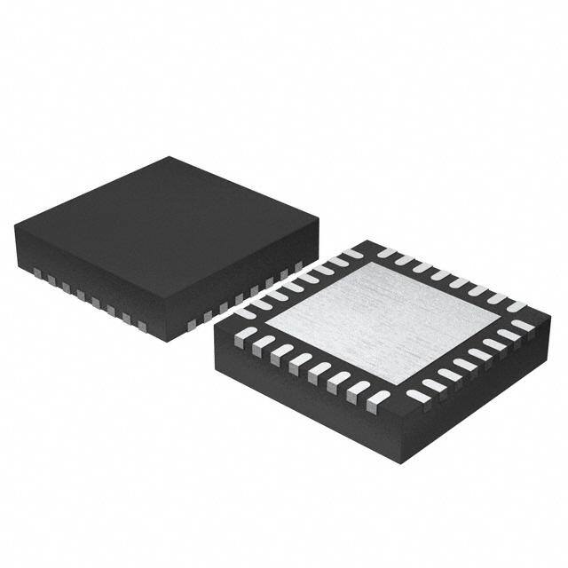
| 供应商器件封装 | 32-QFN(5x5) |
| 信噪比 | Yes |
| 其它名称 | 598-1191 |
| 分辨率 | 24 bit |
| 分辨率(位) | 24 b |
| 功耗 | 60 mW |
| 包装 | 托盘 |
| 商标 | Cirrus Logic |
| 商标名 | CS53L |
| 安装类型 | 表面贴装 |
| 安装风格 | SMD/SMT |
| 封装 | Tube |
| 封装/外壳 | 32-QFN |
| 封装/箱体 | QFN-32 |
| 工作温度 | -10°C ~ 70°C |
| 工作电源电压 | 1.8 V, 2.5 V |
| 工厂包装数量 | 60 |
| 数据接口 | 串行 |
| 最大工作温度 | + 70 C |
| 最小工作温度 | - 10 C |
| 标准包装 | 60 |
| 电压-电源 | 1.65 V ~ 1.89 V,2.37 V ~ 2.63 V |
| 电压源 | 模拟和数字 |
| 电源电压-最大 | 2.63 V |
| 电源电压-最小 | 1.65 V |
| 类型 | ADC, 音频 |
| 系列 | CS53L21 |
| 转换器数量 | 2 |
| 转换速率 | 96 kS/s |
| 配用 | /product-detail/zh/CDB53L21/598-1550-ND/2024832 |
| 采样率(每秒) | 96k |


.jpg)


- 商务部:美国ITC正式对集成电路等产品启动337调查
- 曝三星4nm工艺存在良率问题 高通将骁龙8 Gen1或转产台积电
- 太阳诱电将投资9.5亿元在常州建新厂生产MLCC 预计2023年完工
- 英特尔发布欧洲新工厂建设计划 深化IDM 2.0 战略
- 台积电先进制程称霸业界 有大客户加持明年业绩稳了
- 达到5530亿美元!SIA预计今年全球半导体销售额将创下新高
- 英特尔拟将自动驾驶子公司Mobileye上市 估值或超500亿美元
- 三星加码芯片和SET,合并消费电子和移动部门,撤换高东真等 CEO
- 三星电子宣布重大人事变动 还合并消费电子和移动部门
- 海关总署:前11个月进口集成电路产品价值2.52万亿元 增长14.8%


PDF Datasheet 数据手册内容提取
CS53L21 Low-Power, Stereo Analog-to-Digital Converter FEATURES SYSTEM FEATURES 98-dB dynamic range (A-weighted) 24-bit conversion –88-dB THD+N 4–96 kHz sample rate Analog gain controls Multibit delta–sigma architecture – +32-dB or +16-dB mic preamps – Analog programmable gain amplifier (PGA) Low power operation – Stereo record (ADC): 8.72 mW @ 1.8 V +20-dB digital boost Programmable automatic level control (ALC) – Stereo record (mic to PGA and ADC): 13.73 mW @ 1.8 V – Noise gate for noise suppression Variable power supplies – Programmable threshold and attack/release rates – 1.8–2.5-V digital and analog Independent left/right channel control – 1.8–3.3-V interface logic Digital volume control Power down management High-pass filter disable for DC measurements – ADC, mic preamplifier, PGA Stereo 3:1 analog input MUX Dual mic inputs Software Mode (I²C™ and SPI™ control) – Programmable, low noise mic bias levels Hardware Mode (standalone control) – Differential mic mix for common mode Flexible clocking options noise rejection – Master or slave operation Very low 64 Fs oversampling clock reduces power consumption Digital routing mixes – Mono mixes 1.8 V to 3.3 V 1.8 V to 2.5 V Hardware Mode Digital or I2C & SPI e Signal SofCtwonatrreo MlR Deosadeteat anslator erial Interfac PrEoncgeisnseing ALC OveMrsualtmibpitling MUX PGA SStteerreeoo IInnppuutt 12 SeriaOl Auutpduiot Level Tr PCM S HiFgihlt ePrasss CVoonlutrmoels MAuDltCibit MUX +32dB MSteicr eInop Iuntp 1u t& 3 2 / Oversampling MUX PGA +32dB ADC MIC Register ALC Bias Configuration Copyright Cirrus Logic, Inc. 2005–2015 DS700F1 (All Rights Reserved) JUL ‘15 http://www.cirrus.com
CS53L21 APPLICATIONS GENERAL DESCRIPTION Portable audio players The CS53L21 is a highly integrated, 24-bit, 96-kHz, low power stereo A/D. Based on multibit, delta–sigma mod- Digital microphones ulation, it allows infinite sample rate adjustment between 4 kHz and 96 kHz. The ADC offers many fea- Digital voice recorders tures suitable for low power, portable system Voice recognition systems applications. Audio/video capture cards The ADC input path allows independent channel control of a number of features. An input multiplexer selects be- tween line-level or microphone-level inputs for each channel. The microphone input path includes a select- able programmable-gain preamp stage and a low noise MIC bias voltage supply. A PGA is available for line or microphone inputs and provides analog gain with soft ramp and zero cross transitions. The ADC also features a digital volume attenuator with soft ramp transitions. A programmable ALC and Noise Gate monitor the input signals and adjust the volume levels appropriately. The Signal Processing Engine (SPE) controls left/right channel volume mixing, channel swap and channel mute functions. All volume-level changes may be con- figured to occur on soft ramp and zero cross transitions. The CS53L21 is available in a 32-pin QFN package in both Commercial (-10 to +70° C) and Automotive grades (-40 to +85° C). The CDB53L21 Customer Demonstration board is also available for device evalu- ation and implementation suggestions. Please see “Ordering Information” on page56 for complete details. In addition to its many features, the CS53L21 operates from a low-voltage analog and digital core, making this A/D ideal for portable systems that require extremely low power consumption in a minimal amount of space. 2 DS700F1
CS53L21 TABLE OF CONTENTS 1. PIN DESCRIPTIONS - SOFTWARE (HARDWARE) MODE ..................................................................6 1.1 Digital I/O Pin Characteristics ...........................................................................................................8 2. TYPICAL CONNECTION DIAGRAMS ...................................................................................................9 3. CHARACTERISTIC AND SPECIFICATION TABLES .........................................................................11 SPECIFIED OPERATING CONDITIONS .............................................................................................11 ABSOLUTE MAXIMUM RATINGS .......................................................................................................11 ANALOG CHARACTERISTICS (COMMERCIAL - CNZ) .....................................................................12 ANALOG CHARACTERISTICS (AUTOMOTIVE - DNZ) ......................................................................13 ADC DIGITAL FILTER CHARACTERISTICS .......................................................................................14 SWITCHING SPECIFICATIONS - SERIAL PORT ...............................................................................14 SWITCHING SPECIFICATIONS - I²C CONTROL PORT .....................................................................16 SWITCHING CHARACTERISTICS - SPI CONTROL PORT ................................................................17 DC ELECTRICAL CHARACTERISTICS ..............................................................................................18 DIGITAL INTERFACE SPECIFICATIONS AND CHARACTERISTICS ................................................18 POWER CONSUMPTION ....................................................................................................................19 4. APPLICATIONS ...................................................................................................................................20 4.1 Overview .........................................................................................................................................20 4.1.1 Architecture ...........................................................................................................................20 4.1.2 Line and MIC Inputs ..............................................................................................................20 4.1.3 Signal Processing Engine .....................................................................................................20 4.1.4 Device Control (Hardware or Software Mode) ......................................................................20 4.1.5 Power Management ..............................................................................................................20 4.2 Hardware Mode ..............................................................................................................................21 4.3 Analog Inputs ..................................................................................................................................22 4.3.1 Digital Code, Offset and DC Measurement ...........................................................................22 4.3.2 High-Pass Filter and DC Offset Calibration ...........................................................................23 4.3.3 Digital Routing .......................................................................................................................23 4.3.4 Differential Inputs ..................................................................................................................23 4.3.4.1 External Passive Components ...................................................................................23 4.3.5 Analog Input Multiplexer ........................................................................................................24 4.3.6 MIC and PGA Gain ................................................................................................................25 4.3.7 Automatic Level Control (ALC) ..............................................................................................25 4.3.8 Noise Gate ............................................................................................................................26 4.4 Signal Processing Engine ...............................................................................................................27 4.4.1 Volume Controls ....................................................................................................................27 4.4.2 Mono Channel Mixer .............................................................................................................27 4.5 Serial Port Clocking ........................................................................................................................28 4.5.1 Slave .....................................................................................................................................28 4.5.2 Master ...................................................................................................................................29 4.5.3 High-Impedance Digital Output .............................................................................................29 4.5.4 Quarter- and Half-Speed Mode .............................................................................................29 4.6 Digital Interface Formats ................................................................................................................30 4.7 Initialization .....................................................................................................................................30 4.8 Recommended Power-Up Sequence .............................................................................................30 4.9 Recommended Power-Down Sequence ........................................................................................31 4.10 Software Mode .............................................................................................................................31 4.10.1 SPI Control ..........................................................................................................................32 4.10.2 I²C Control ...........................................................................................................................32 4.10.3 Memory Address Pointer (MAP) ..........................................................................................33 4.10.3.1 Map Increment (INCR) .............................................................................................33 5. REGISTER QUICK REFERENCE ........................................................................................................34 6. REGISTER DESCRIPTION ..................................................................................................................36 DS700F1 3
CS53L21 6.1 Chip I.D. and Revision Register (Address 01h) (Read Only) .........................................................36 6.2 Power Control 1 (Address 02h) ......................................................................................................36 6.3 MIC Power Control and Speed Control (Address 03h) ...................................................................37 6.4 Interface Control (Address 04h) .....................................................................................................39 6.5 MIC Control (Address 05h) .............................................................................................................40 6.6 ADC Control (Address 06h) ............................................................................................................41 6.7 ADCx Input Select, Invert and Mute (Address 07h) ........................................................................42 6.8 SPE Control (Address 09h) ............................................................................................................43 6.9 ALCX and PGAX Control: ALCA, PGAA (Address 0Ah) and ALCB, PGAB (Address 0Bh) ..........45 6.10 ADCx Attenuator: ADCA (Address 0Ch) and ADCB (Address 0Dh) ............................................46 6.11 ADCx Mixer Volume Control: ADCA (Address 0Eh) and ADCB (Address 0Fh) ...........................46 6.12 Channel Mixer (Address 18h) .......................................................................................................47 6.13 ALC Enable and Attack Rate (Address 1Ch) ................................................................................47 6.14 ALC Release Rate (Address 1Dh) ................................................................................................48 6.15 ALC Threshold (Address 1Eh) ......................................................................................................48 6.16 Noise Gate Configuration and Misc. (Address 1Fh) .....................................................................49 6.17 Status (Address 20h) (Read Only) ...............................................................................................50 7. ANALOG PERFORMANCE PLOTS ....................................................................................................51 7.1 ADC_FILT+ Capacitor Effects on THD+N ......................................................................................51 8. EXAMPLE SYSTEM CLOCK FREQUENCIES ....................................................................................51 8.1 Auto Detect Enabled .......................................................................................................................51 8.2 Auto Detect Disabled ......................................................................................................................52 9. PCB LAYOUT CONSIDERATIONS .....................................................................................................52 9.1 Power Supply, Grounding ...............................................................................................................52 9.2 QFN Thermal Pad ..........................................................................................................................53 10. DIGITAL FILTERS ..............................................................................................................................53 11. PARAMETER DEFINITIONS ..............................................................................................................54 12. PACKAGE DIMENSIONS .................................................................................................................55 THERMAL CHARACTERISTICS ..........................................................................................................55 13. ORDERING INFORMATION .............................................................................................................56 14. REFERENCES ....................................................................................................................................56 15. REVISION HISTORY .........................................................................................................................56 LIST OF FIGURES Figure 1.Typical Connection Diagram (Software Mode) .............................................................................9 Figure 2.Typical Connection Diagram (Hardware Mode) ..........................................................................10 Figure 3.Serial Audio Interface Slave Mode Timing ..................................................................................15 Figure 4.Serial Audio Interface Master Mode Timing ................................................................................15 Figure 5.Control Port Timing - I²C .............................................................................................................16 Figure 6.Control Port Timing - SPI Format ................................................................................................17 Figure 7.Analog Input Architecture ............................................................................................................22 Figure 8.MIC Input Mix w/Common Mode Rejection .................................................................................24 Figure 9.Differential Input ..........................................................................................................................24 Figure 10.ALC ...........................................................................................................................................25 Figure 11.Noise Gate Attenuation .............................................................................................................26 Figure 12.Signal Processing Engine .........................................................................................................27 Figure 13.Master Mode Timing .................................................................................................................29 Figure 14.Tri-State Serial Port ..................................................................................................................29 Figure 15.I²S Format .................................................................................................................................30 Figure 16.Left-Justified Format .................................................................................................................30 Figure 17.Initialization Flow Chart .............................................................................................................31 Figure 18.Control Port Timing in SPI Mode ..............................................................................................32 Figure 19.Control Port Timing, I²C Write ...................................................................................................33 Figure 20.Control Port Timing, I²C Read ...................................................................................................33 4 DS700F1
CS53L21 Figure 21.AIN and PGA Selection .............................................................................................................43 Figure 22.ADC THD+N vs. Frequency w/Capacitor Effects ......................................................................51 Figure 23.ADC Passband Ripple ..............................................................................................................53 Figure 24.ADC Stopband Rejection ..........................................................................................................53 Figure 25.ADC Transition Band ................................................................................................................53 Figure 26.ADC Transition Band Detail ......................................................................................................53 LIST OF TABLES Table 1. I/O Power Rails .............................................................................................................................8 Table 2. Hardware Mode Feature Summary .............................................................................................21 Table 3. MCLK/LRCK Ratios ....................................................................................................................28 DS700F1 5
CS53L21 1. PIN DESCRIPTIONS - SOFTWARE (HARDWARE) MODE S) M/ T ( T TSTN SCLK MCLK SDOU DGND VD VL RESE 32 31 30 29 28 27 26 25 LRCK 1 24 AIN1B SDA/CDIN (MCLKDIV2) 2 23 AIN1A SCL/CCLK (I²S/LJ) 3 22 AFILTB AD0/CS (TSTN) 4 CS53L21 21 AFILTA VA_PULLUP 5 20 AIN2B/BIAS TSTO 6 19 AIN2A AGND 7 18 MICIN2/BIAS/AIN3B TSTO 8 17 MICIN1/AIN3A 9 10 11 12 13 14 15 16 TO NIC NIC VA ND TO VQ LT+ TS AG TS FI Pin Name # Pin Description Left Right Clock (Input/Output) - Determines which channel, Left or Right, is currently active on the LRCK 1 serial audio data line. Serial Control Data (Input/Output) - SDA is a data I/O in I²C Mode. CDIN is the input data line for the SDA/CDIN 2 control port interface in SPI Mode. (MCLKDIV2) MCLK Divide by 2 (Input) - Hardware Mode: Divides the MCLK by 2 prior to all internal circuitry. Serial Control Port Clock (Input) - Serial clock for the serial control port. SCL/CCLK 3 (I²S/LJ) Interface Format Selection (Input) - Hardware Mode: Selects between I²S and left-Justified interface formats for the ADC. Address Bit 0 (I²C) / Control Port Chip Select (SPI) (Input) - AD0 is a chip address pin in I²C Mode; CS AD0/CS is the chip-select signal for SPI format. 4 (TSTN) Test In (Input) - Hardware Mode: This pin is an input used for test purposes only and should be tied to DGND for normal operation. Reference Pull-up (Input) - This pin is an input used for test purposes only and must be pulled-up to VA VA_PULLUP 5 using a 47 k resistor. Test Out (Output) - This pin is an output used for test purposes only and must be left “floating” (no con- TSTO 6 nection external to the pin). AGND 7 Analog Ground (Input) - Ground reference for the internal analog section. Test Out (Output) - This pin is an output used for test purposes only and must be left “floating” (no con- TSTO 8 nection external to the pin). 6 DS700F1
CS53L21 Test Out (Output) - This pin is an output used for test purposes only and must be left “floating” (no con- TSTO 9 nection external to the pin). NIC 10 .Not Internally Connected - This pin is not connected internal to the device and may be connected to NIC 11 ground or left “floating”. No other external connection should be made to this pin. VA 12 Analog Power (Input) - Positive power for the internal analog section. AGND 13 Analog Ground (Input) - Ground reference for the internal analog section. Test Out (Output) - This pin is an output used for test purposes only and must be left “floating” (no con- TSTO 14 nection external to the pin). VQ 15 Quiescent Voltage (Output) - Filter connection for internal quiescent voltage. FILT+ 16 Positive Voltage Reference (Output) - Positive reference voltage for the internal sampling circuits. MICIN1/ Microphone Input 1 (Input) - The full-scale level is specified in the ADC Analog Characteristics specifi- 17 AIN3A cation table. Microphone Input 2 (Input/Output) - The full-scale level is specified in the ADC Analog Characteristics MICIN2/ 18 specification table. This pin can also be configured as an output to provide a low noise bias supply for an BIAS/AIN3B external microphone. Electrical characteristics are specified in the DC Electrical Characteristics table. Analog Input(Input) - The full-scale level is specified in the ADC Analog Characteristics specification AIN2A 19 table. Analog Input(Input/Output) - The full-scale level is specified in the ADC Analog Characteristics specifi- AIN2B/BIAS 20 cation table. This pin can also be configured as an output to provide a low noise bias supply for an exter- nal microphone. Electrical characteristics are specified in the DC Electrical Characteristics table. AFILTA 21 Filter Connection (Output) - Filter connection for the ADC inputs. AFILTB 22 AIN1A 23 Analog Input(Input) - The full-scale level is specified in the ADC Analog Characteristics specification AIN1B 24 table. RESET 25 Reset (Input) - The device enters a low power mode when this pin is driven low. Digital Interface Power (Input) - Determines the required signal level for the serial audio interface and VL 26 host control port. Refer to the Recommended Operating Conditions for appropriate voltages. VD 27 Digital Power (Input) - Positive power for the internal digital section. DGND 28 Digital Ground (Input) - Ground reference for the internal digital section. Serial Audio Data Output(Output) - Output for two’s complement serial audio data. SDOUT 29 Serial Port Master/Slave (Input/Output) - Hardware Mode Startup Option: Selects between Master and (M/S) Slave Mode for the serial port. MCLK 30 Master Clock (Input) - Clock source for the delta-sigma modulators. SCLK 31 Serial Clock (Input/Output) -- Serial clock for the serial audio interface. Test In (Input) - This pin is an input used for test purposes only and should be tied to DGND for normal TSTN 32 operation. Thermal Pad - Thermal relief pad for optimized heat dissipation. See “QFN Thermal Pad” on page53. DS700F1 7
CS53L21 1.1 Digital I/O Pin Characteristics The logic level for each input should not exceed the maximum ratings for the VL power supply. Pin Name I/O Driver Receiver SW/(HW) RESET Input - 1.8 V - 3.3 V SCL/CCLK Input - 1.8 V - 3.3 V, with Hysteresis (I²S/LJ) SDA/CDIN Input/Output 1.8 V - 3.3 V, CMOS/Open Drain 1.8 V - 3.3 V, with Hysteresis (MCLKDIV2) AD0/CS Input - 1.8 V - 3.3 V (DEM) MCLK Input - 1.8 V - 3.3 V LRCK Input/Output 1.8 V - 3.3 V, CMOS 1.8 V - 3.3 V SCLK Input/Output 1.8 V - 3.3 V, CMOS 1.8 V - 3.3 V SDOUT Input/Output 1.8 V - 3.3 V, CMOS 1.8 V - 3.3 V (M/S) Table 1. I/O Power Rails 8 DS700F1
CS53L21 2. TYPICAL CONNECTION DIAGRAMS +1.8 V or +2.5 V See Note 4 +1.8 V or +2.5 V 1 µF 0.1 µF 0.1 µF 1 µF 47 k Note 4: Series resistance in the path of the power supplies must be avoided. VD VA VA_ PULLUP CS53L21 AIN1A Left Analog Input 1 TSTN 1800 pF * 1 µF 100 100 k 1800 pF * 100 1 00 k MCLK AIN1B Right Analog Input 1 SCLK 1 µF LRCK AIN2A Left Analog Input 2 1800 pF * 1 µF 100 100 k Digital Audio Processor SDOUT 1800 pF * 1 00 k AIN2B 100 RESET Right Analog Input 2 BIAS1 1 µF SCL/CCLK MICIN1 SDA/CDIN Microphone Input AIN3A AD0/CS 1 µF 100 k BIAS2 Microphone Bias AIN3B/MICIN2 0.1 µF RL See Note 3 2 k 2 k Note 3: The value of RL is dictated by the microphone cartridge. +1.8 V, +2.5 V See Note 1 or +3.3 V VL FILT+ 0.1 µF Note 1: Resistors are required for I²C control port operation 10 µF AGND * * 150 pF 150 pF AFILTA 1 µF AFILTB VQ * Capacitors must be C0G or equivalent DGND Figure 1. Typical Connection Diagram (Software Mode) DS700F1 9
CS53L21 +1.8V or +2.5V See Note 4 +1.8V or +2.5V 1 µF 0.1 µF 0.1 µF 47 k Note 4: VD VA VA_ Series resistance in the path of the power supplies PULLUP (typically used for added filtering ) must be avoided. CS53L21 TSTN MCLK SCLK LRCK AIN1A Left Analog Input 1 VL or DGND (1) 1800 pF * 1 µF 100 100 k SDOUT/ DPigriotacle Asusodrio M/S 1800 pF * 100 100 k AIN1B Right Analog Input 1 RESET 1 µF I²S/LJ FILT+ MCLKDIV2 DEM 10 µF AGND * * 150 pF 150 pF AFILTA 1 µF +1.8V, 2.5 V VL AFILTB or +3.3V VQ 0.1 µF * Capacitors must be C0G or equivalent DGND (1) Pull-up to VL (47 kfor Master Mode. Pull-down to DGND for Slave Mode . Figure 2. Typical Connection Diagram (Hardware Mode) 10 DS700F1
CS53L21 3. CHARACTERISTIC AND SPECIFICATION TABLES (All Min/Max characteristics and specifications are guaranteed over the Specified Operating Conditions. Typical per- formance characteristics and specifications are derived from measurements taken at nominal supply voltages and T = 25° C.) A SPECIFIED OPERATING CONDITIONS (AGND=DGND=0 V, all voltages with respect to ground.) Parameters Symbol Min Max Units DC Power Supply (Note 1) Analog Core VA 1.65 2.63 V Digital Core VD 1.65 2.63 V Serial/Control Port Interface VL 1.65 3.47 V Ambient Temperature Commercial - CNZ -10 +70 C T Automotive - DNZ A -40 +85 C Note: 1. The device will operate properly over the full range of the analog, digital core and serial/control port in- terface supplies. ABSOLUTE MAXIMUM RATINGS (AGND = DGND = 0 V; all voltages with respect to ground.) Parameters Symbol Min Max Units DC Power Supply Analog VA -0.3 3.0 V Digital VD -0.3 3.0 V Serial/Control Port Interface VL -0.3 4.0 V Input Current (Note 2) Iin - ±10 mA Analog Input Voltage (Note 3) VIN AGND-0.7 VA+0.7 V Digital Input Voltage V -0.3 VL+ 0.4 V (Note 3) IND Ambient Operating Temperature (power applied) TA -50 +115 °C Storage Temperature Tstg -65 +150 °C WARNING:Operation at or beyond these limits may result in permanent damage to the device. Normal operation is not guaranteed at these extremes. Notes: 2. Any pin except supplies. Transient currents of up to ±100 mA on the analog input pins will not cause SCR latch-up. 3. The maximum over/under voltage is limited by the input current. DS700F1 11
CS53L21 ANALOG CHARACTERISTICS (COMMERCIAL - CNZ) (Test Conditions (unless otherwise specified): Input sine wave (relative to digital full scale): 1kHz through passive input filter; Measurement Bandwidth is 10Hz to 20kHz unless otherwise specified. Sample Frequency = 48kHz) VA = 2.5 V (nominal) VA = 1.8 V (nominal) Parameter (Note 4) Min Typ Max Min Typ Max Unit Analog In to ADC (PGA bypassed) Dynamic Range A-weighted 93 99 - 90 96 - dB unweighted 90 96 - 87 93 - dB Total Harmonic Distortion + Noise -1dBFS - -86 -80 - -84 -78 dB -20dBFS - -76 - - -73 - dB -60dBFS - -36 - - -33 - dB Analog In to PGA to ADC Dynamic Range PGA Setting: 0 dB A-weighted 92 98 - 89 95 - dB unweighted 89 95 - 86 92 - dB PGA Setting: +12 dB A-weighted 85 91 - 82 88 - dB unweighted 82 88 - 79 85 - dB Total Harmonic Distortion + Noise PGA Setting: 0 dB -1dBFS - -88 -81 - -86 -80 dB -60dBFS - -35 - - -32 - dB PGA Setting: +12 dB -1dBFS - -85 -79 - -83 -77 dB Analog In to MIC Pre-Amp (+16 dB) to PGA to ADC Dynamic Range PGA Setting: 0 dB A-weighted - 86 - - 83 - dB unweighted - 83 - - 80 - dB Total Harmonic Distortion + Noise PGA Setting: 0 dB -1dBFS - -76 - - -74 - dB Analog In to MIC Pre-Amp (+32 dB) to PGA to ADC Dynamic Range PGA Setting: 0 dB A-weighted - 78 - - 75 - dB unweighted - 74 - - 71 - dB Total Harmonic Distortion + Noise PGA Setting: 0 dB -1dBFS - -74 - - -71 - dB Other Characteristics DC Accuracy Interchannel Gain Mismatch - 0.2 - - 0.2 - dB Gain Drift - ±100 - - ±100 - ppm/°C Offset Error SDOUT Code with HPF On - 352 - - 352 - LSB Input Interchannel Isolation - 90 - - 90 - dB Full-scale Input Voltage ADC 0.74•VA 0.78•VA 0.82•VA 0.74•VA 0.78•VA 0.82•VA Vpp PGA (0 dB) 0.75•VA 0.794•VA 0.83•VA 0.75•VA 0.794•VA 0.83•VA Vpp MIC (+16 dB) 0.129•VA 0.129•VA Vpp MIC (+32 dB) 0.022•VA 0.022•VA Vpp Input Impedance (Note 5) ADC - 20 - - 20 - k PGA - 39 - - 39 - k MIC - 50 - - 50 - k 4. Referred to the typical full-scale voltage. Applies to all THD+N and Dynamic Range values in the table. 5. Measured between AINxx and AGND. 12 DS700F1
CS53L21 ANALOG CHARACTERISTICS (AUTOMOTIVE - DNZ) (Test Conditions (unless otherwise specified): Input sine wave (relative to full scale): 1 kHz through passive input filter; Measurement Bandwidth is 10Hz to 20kHz unless otherwise specified. Sample Frequency = 48kHz) VA = 2.5 V (nominal) VA = 1.8 V (nominal) Parameter (Note 4) Min Typ Max Min Typ Max Unit Analog In to ADC Dynamic Range A-weighted 91 99 - 88 96 - dB unweighted 78 96 - 85 93 - dB Total Harmonic Distortion + Noise -1dBFS - -86 -78 - -84 -76 dB -20dBFS - -76 - - -73 - dB -60dBFS - -36 - - -33 - dB Analog In to PGA to ADC Dynamic Range PGA Setting: 0 dB A-weighted 90 98 - 87 95 - dB unweighted 87 95 - 84 92 - dB PGA Setting: +12 dB A-weighted 83 91 - 80 88 - dB unweighted 80 88 - 77 85 - dB Total Harmonic Distortion + Noise PGA Setting: 0 dB -1dBFS - -88 -80 - -86 -78 dB -60dBFS - -35 - - -32 - dB PGA Setting: +12 dB -1dBFS - -85 -77 - -83 -75 dB Analog In to MIC Pre-Amp (+16 dB) to PGA to ADC Dynamic Range PGA Setting: 0 dB A-weighted - 86 - - 83 - dB unweighted - 83 - - 80 - dB Total Harmonic Distortion + Noise PGA Setting: 0 dB -1dBFS - -76 - - -74 - dB Analog In to MIC Pre-Amp (+32 dB) to PGA to ADC Dynamic Range PGA Setting: 0 dB A-weighted - 78 - - 75 - dB unweighted - 74 - - 71 - dB Total Harmonic Distortion + Noise PGA Setting: 0 dB -1dBFS - -74 - - -71 - dB Other Characteristics DC Accuracy Interchannel Gain Mismatch - 0.1 - - 0.1 - dB Gain Drift - ±100 - - ±100 - ppm/°C Offset Error SDOUT Code with HPF On - 352 - - 352 - LSB Input Interchannel Isolation - 90 - - 90 - dB Full-scale Input Voltage ADC 0.74•VA 0.78•VA 0.82•VA 0.74•VA 0.78•VA 0.82•VA Vpp PGA (0 dB) 0.75•VA 0.794•VA 0.83•VA 0.75•VA 0.794•VA 0.83•VA Vpp MIC (+16 dB) 0.129•VA 0.129•VA Vpp MIC (+32 dB) 0.022•VA 0.022•VA Vpp Input Impedance (Note 5) ADC 18 - - 18 - - k PGA 40 - - 40 - - k MIC 50 - - 50 - - k DS700F1 13
CS53L21 ADC DIGITAL FILTER CHARACTERISTICS Parameter (Note 6) Min Typ Max Unit Passband (Frequency Response) to -0.1 dB corner 0 - 0.46 Fs Passband Ripple -0.09 - 0.17 dB Stopband 0.6 - - Fs Stopband Attenuation 33 - - dB Total Group Delay - 7.6/Fs - s High-Pass Filter Characteristics (48 kHz Fs) Frequency Response -3.0 dB - 3.7 - Hz -0.13 dB - 24.2 - Hz Phase Deviation @ 20Hz - 10 - Deg Passband Ripple - - 0.17 dB Filter Settling Time - 105/Fs 0 s 6. Response is clock-dependent and will scale with Fs. Note that the response plots (Figures23 to26) have been normalized to Fs and can be denormalized by multiplying the X-axis scale by Fs. HPF parameters are for Fs = 48 kHz. SWITCHING SPECIFICATIONS - SERIAL PORT (Inputs: Logic 0 = DGND, Logic 1 = VL, SDOUT C = 15 pF.) LOAD Parameters Symbol Min Max Units RESET pin Low Pulse Width (Note 7) 1 - ms MCLK Frequency 1.024 38.4 MHz MCLK Duty Cycle (Note 8) 45 55 % Slave Mode Input Sample Rate (LRCK) Quarter-Speed Mode Fs 4 12.5 kHz Half-Speed Mode Fs 8 25 kHz Single-Speed Mode Fs 4 50 kHz Double-Speed Mode Fs 50 100 kHz LRCK Duty Cycle 45 55 % SCLK Frequency 1/tP - 64•Fs Hz SCLK Duty Cycle 45 55 % LRCK Setup Time Before SCLK Rising Edge ts(LK-SK) 40 - ns LRCK Edge to SDOUT MSB Output Delay td(MSB) - 52 ns SDOUT Setup Time Before SCLK Rising Edge ts(SDO-SK) 20 - ns SDOUT Hold Time After SCLK Rising Edge th(SK-SDO) 30 - ns 14 DS700F1
CS53L21 Parameters Symbol Min Max Units Master Mode (Note 9) Output Sample Rate (LRCK) All Speed Modes MCLK F - ----------------- Hz (Note 10) s 128 LRCK Duty Cycle 45 55 % SCLK Frequency 1/tP - 64•Fs Hz SCLK Duty Cycle 45 55 % LRCK Edge to SDOUT MSB Output Delay td(MSB) - 52 ns SDOUT Setup Time Before SCLK Rising Edge ts(SDO-SK) 20 - ns SDOUT Hold Time After SCLK Rising Edge th(SK-SDO) 30 - ns 7. After powering up the CS53L21, RESET should be held low after the power supplies and clocks are settled. 8. See “Example System Clock Frequencies” on page51 for typical MCLK frequencies. 9. See“Master” on page29. 10. “MCLK” refers to the external master clock applied. // LRCK // t t s(LK-SK) P // SCLK // t t t d(MSB) h(SK-SDO) s(SDO-SK) // SDOUT MSB MSB-1 // Figure 3. Serial Audio Interface Slave Mode Timing // LRCK // t P // SCLK // t t t d(MSB) h(SK-SDO) s(SDO-SK) // SDOUT MSB MSB-1 // Figure 4. Serial Audio Interface Master Mode Timing DS700F1 15
CS53L21 SWITCHING SPECIFICATIONS - I²C CONTROL PORT (Inputs: Logic 0=DGND, Logic 1=VL, SDA C =30pF) L Parameter Symbol Min Max Unit SCL Clock Frequency fscl - 100 kHz RESET Rising Edge to Start tirs 500 - ns Bus Free Time Between Transmissions tbuf 4.7 - µs Start Condition Hold Time (prior to first clock pulse) thdst 4.0 - µs Clock Low time tlow 4.7 - µs Clock High Time thigh 4.0 - µs Setup Time for Repeated Start Condition tsust 4.7 - µs SDA Hold Time from SCL Falling (Note 11) thdd 0 - µs SDA Setup time to SCL Rising tsud 250 - ns Rise Time of SCL and SDA trc - 1 µs Fall Time SCL and SDA tfc - 300 ns Setup Time for Stop Condition tsusp 4.7 - µs Acknowledge Delay from SCL Falling tack 300 3450 ns 11. Data must be held for sufficient time to bridge the transition time, t , of SCL. fc RST t irs Repeated Stop Start Start Stop SDA tbuf thdst thigh thdst tf tsusp SCL tlow thdd tsud tsust tr Figure 5. Control Port Timing - I²C 16 DS700F1
CS53L21 SWITCHING CHARACTERISTICS - SPI CONTROL PORT (Inputs: Logic 0=DGND, Logic 1=VL) Parameter Symbol Min Max Units CCLK Clock Frequency fsck 0 6.0 MHz RESET Rising Edge to CS Falling tsrs 20 - ns CS Falling to CCLK Edge tcss 20 - ns CS High Time Between Transmissions tcsh 1.0 - s CCLK Low Time tscl 66 - ns CCLK High Time tsch 66 - ns CDIN to CCLK Rising Setup Time tdsu 40 - ns CCLK Rising to DATA Hold Time (Note 12) tdh 15 - ns Rise Time of CCLK and CDIN (Note 13) tr2 - 100 ns Fall Time of CCLK and CDIN (Note 13) tf2 - 100 ns 12. Data must be held for sufficient time to bridge the transition time of CCLK. 13. For f <1MHz. sck RST t srs CS t csh t t t css sch scl t r2 CCLK t f2 t t dsu dh CDIN Figure 6. Control Port Timing - SPI Format DS700F1 17
CS53L21 DC ELECTRICAL CHARACTERISTICS (AGND = 0 V; all voltages with respect to ground.) Parameters Min Typ Max Units VQ Characteristics Nominal Voltage - 0.5•VA - V Output Impedance - 23 - k DC Current Source/Sink (Note 14) - - 10 A FILT+ - VA - V MIC BIAS Characteristics Nominal Voltage MICBIAS_LVL[1:0] = 00 - 0.8•VA - V MICBIAS_LVL[1:0] = 01 - 0.7•VA - V MICBIAS_LVL[1:0] = 10 - 0.6•VA - V MICBIAS_LVL[1:0] = 11 - 0.5•VA - V DC Current Source - - 1 mA Power Supply Rejection Ratio (PSRR) 1 kHz - 50 - dB Power Consumption (Normal Operation Worse Case) 1 kHz - - 30 mW Power Supply Rejection Ratio (PSRR) (Note 15) 1 kHz - 60 - dB 14. The DC current draw represents the allowed current draw from the VQ pin due to typical leakage through electrolytic de-coupling capacitors. 15. Valid with the recommended capacitor values on FILT+ and VQ. Increasing the capacitance will also increase the PSRR. DIGITAL INTERFACE SPECIFICATIONS AND CHARACTERISTICS Parameters (Note 16) Symbol Min Max Units Input Leakage Current Iin - ±10 A Input Capacitance - 10 pF 1.8 V - 3.3 V Logic High-Level Output Voltage (IOH = -100 A) VOH VL - 0.2 - V Low-Level Output Voltage (IOL = 100 A) VOL - 0.2 V High-Level Input Voltage VIH 0.68•VL - V Low-Level Input Voltage VIL - 0.32•VL V 16. See “Digital I/O Pin Characteristics” on page8 for serial and control port power rails. 18 DS700F1
CS53L21 POWER CONSUMPTION See (Note 17) Power Control. Typical Current (mA) Registers 02h 03h Operation ved bit 6ved bit 5PGABPGAAADCBADCA MICBMICAMICBIAS iVA iVD (NoitVeL 18) Total serserN_N_N_N_NN_N_N_ Power ReRePDPDPDPDPDPDPDPD V (mWrms) x x x x x x x x x x 1.8 0 0 0 0 1 Off (Note 19) 2.5 0 0 0 0 x x x x x x 1 x x x 1.8 0.01 0.02 0 0.05 2 Standby (Note 20) 2.5 0.01 0.03 0 0.10 3 Mono Record ADC 1 1 1 1 1 0 0 1 1 1 1.8 1.85 2.03 0.03 7.05 2.5 2.07 3.05 0.05 12.94 PGA to ADC 1 1 1 0 1 0 0 1 1 1 1.8 2.35 2.03 0.03 7.95 2.5 2.58 3.08 0.05 14.29 MIC to PGA to ADC 1 1 1 0 1 0 0 1 0 0 1.8 3.67 2.05 0.03 10.36 (with Bias) 2.5 3.95 3.09 0.05 17.71 MIC to PGA to ADC 1 1 1 0 1 0 0 1 0 1 1.8 3.27 2.03 0.03 9.61 (no Bias) 2.5 3.52 3.08 0.05 16.62 4 Stereo Record ADC 1 1 1 1 0 0 0 1 1 1 1.8 2.69 2.12 0.03 8.72 2.5 2.93 3.18 0.04 15.40 PGA to ADC 1 1 0 0 0 0 0 1 1 1 1.8 3.65 2.12 0.03 10.45 2.5 3.91 3.17 0.04 17.84 MIC to PGA to ADC 1 1 0 0 0 0 0 0 0 1 1.8 5.48 2.11 0.03 13.73 (no Bias) 2.5 5.76 3.17 0.04 22.45 17. Unless otherwise noted, test conditions are as follows: All zeros input, slave mode, sample rate = 48kHz; No load. Digital (VD) and logic (VL) supply current will vary depending on speed mode and mas- ter/slave operation. 18. VL current will slightly increase in master mode. 19. RESET pin 25 held LO, all clocks and data lines are held LO. 20. RESET pin 25 held HI, all clocks and data lines are held HI. DS700F1 19
CS53L21 4. APPLICATIONS 4.1 Overview 4.1.1 Architecture The CS53L21 is a highly integrated, low power, 24-bit audio A/D. The ADC operates at 64Fs, where Fs is equal to the system sample rate. The different clock rates maximize power savings while maintaining high performance. The A/D operates in one of four sample rate speed modes: Quarter, Half, Single and Double. It accepts and is capable of generating serial port clocks (SCLK, LRCK) derived from an input Master Clock (MCLK). 4.1.2 Line and MIC Inputs The analog input portion of the A/D allows selection from and configuration of multiple combinations of stereo and microphone (MIC) sources. Six line inputs with configuration for two MIC inputs (or one MIC input with common mode rejection), two MIC bias outputs and independent channel control (including a high-pass filter disable function) are available. A Programmable Gain Amplifier (PGA), MIC boost, and Au- tomatic Level Control (ALC), with noise gate settings, provide analog gain and adjustment. Digital volume controls, including gain, boost, attenuation and inversion are also available. 4.1.3 Signal Processing Engine The ADC data has independent volume controls and mixing functions such as mono mixes and left/right channel swaps. 4.1.4 Device Control (Hardware or Software Mode) In Software Mode, all functions and features may be controlled via a two-wire I²C or three-wire SPI control port interface. In Hardware Mode, a limited feature set may be controlled via stand-alone control pins. 4.1.5 Power Management Two Software Mode control registers provide independent power-down control of the ADC, PGA, MIC pre- amp and MIC bias, allowing operation in select applications with minimal power consumption. 20 DS700F1
CS53L21 4.2 Hardware Mode A limited feature set is available when the A/D powers up in Hardware Mode (see “Recommended Power- Up Sequence” on page30) and may be controlled via stand-alone control pins. Table2 shows a list of func- tions/features, the default configuration and the associated stand-alone control available. Hardware Mode Feature/Function Summary Feature/Function Default Configuration Stand-Alone Control Note Power Control Device Powered Up PGAx Powered Up ADCx Powered Up - - MIC Bias Powered Down MICx Preamp Powered Down Auto-Detect Enabled - - Speed Mode Serial Port Slave Auto-Detect Speed Mode - - Serial Port Master Single-Speed Mode see Section MCLK Divide (Selectable) “MCLKDIV2” pin 2 4.5 on page 28 see Section Serial Port Master / Slave Selection (Selectable) “M/S” pin 29 4.5 on page 28 Interface Control ADC see Section (Selectable) “I²S/LJ” pin 3 4.6 on page 30 ADC Volume and Gain Digital Boost Disabled Soft Ramp Disabled Zero Cross Disabled Invert Disabled - - PGAx 0 dB Attenuator 0 dB ALC Disabled Noise Gate Disabled ADCx High-Pass Filter Enabled - - ADCx High-Pass Filter Freeze Continuous DC Subtraction AIN1A to PGAA Line/MIC Input Select - - AIN1B to PGAB ADC mix Volume and Gain Invert Disabled Soft Ramp Enabled - - Zero Cross Enabled Signal Processing Engine (SPE) MIX Disabled - - Data Selection (SPE Enable) ADC Data to SPE - - Channel Swap ADC ADCA = L; ADCB = R - - Table 2. Hardware Mode Feature Summary DS700F1 21
CS53L21 4.3 Analog Inputs AINxA and AINxB are the analog inputs, internally biased to VQ, that accepts line-level and MIC-level sig- nals, allowing various gain and signal adjustments for each channel. PGAA_VOL[5:0] ADCA_MUTE ADC_SNGVOL SOFTA ADCA_DBOOST ADCA_ATT[7:0] PDN_ADCA ZCROSSA 0/-96dB +12/-3dB 1dB steps 0.5dB steps AIN1A +20dB Multibit AIN2A Digital Attenuator Oversampling PGA MUX MUX MUX AADDCCAA__HHPPFF FERNEAEBZLEE Boost SOFTA INV_ADACDAC PDN_PGAA 3+216d/B AIN3A/ MICIN1 ALCA_SRDIS AINA_MUX[1:0] MICA_BOOST ALCA_ZCDIS PDN_MICA ALC_ENA MICBIAS_LVL[1:0] M Serial Interface DIGMIX MICMIX AALLCC__RAAARRLLMAAMCCAATTIBBLNEXE__C[[[[SZ2255_::::CRE0000DD]]]]NIIBSS ALC Noise Gate NNTNHGGGR__DEAEESLNLLHAY[3[:10:]0] PDN_MICBIAS MICMBIICABSIAS_SEL PC PGAB_VOL[5:0] ADC_SNGVOL SOFTB ADCB_DBOOST PDN_ADCB ZCROSSB SOFTB +12/-3dB 0.5dB steps AIN1B MUX +20dB Multibit AIN2B/MICBIAS MUX Digital Attenuator Oversampling PGA MUX Boost ADC AIN3B/ MICIN2/ AADDCCBB__HHPPFF FERNEAEBZLEE ADCB_MUTE INV_ADCB PDN_PGAB 3+216d/B MICBIAS ADCB_ATT[7:0] AINB_MUX[1:0] MICB_BOOST PDN_MICB 0/-96dB 1dB steps TO SIGNAL PROCESSING ENGINE (SPE) FROM SIGNAL PROCESSING ENGINE (SPE) Figure 7. Analog Input Architecture 4.3.1 Digital Code, Offset and DC Measurement The ADC output data is in two’s complement binary format. For inputs above positive full scale or below negative full scale, the ADC will output 7FFFFFH or 800000H, respectively and cause the ADC overflow bit to be set to a ‘1’. Given the two’s complement format, low-level signals may cause the MSB of the serial data to periodically toggle between ‘1’ and ‘0’, possibly introducing noise into the system as the bit switches back and forth. To prevent this phenomena, a constant DC offset is added to the serial data bringing the low-level signal just above the point at which the MSB would normally toggle, thus reducing the noise introduced. Note that this offset is not removed (refer to “Analog Characteristics (Commercial - CNZ)” on page12 and/or “Analog Characteristics (Automotive - DNZ)” on page13 for the specified offset level). The A/D may be used to measure DC voltages by disabling the high-pass filter for the designated channel. DC levels are measured relative to VQ and will be decoded as positive two’s complement binary numbers above VQ and negative two’s complement binary numbers below VQ. Software “Status (Address 20h) (Read Only)” on page50, “ADC Control (Address 06h)” on page41. Controls: 22 DS700F1
CS53L21 4.3.2 High-Pass Filter and DC Offset Calibration The high-pass filter continuously subtracts a measure of the DC offset from the output of the decimation filter. If the high-pass filter is “frozen” during normal operation, the current value of the DC offset for the corresponding channel is held. It is this DC offset that will continue to be subtracted from the conversion result. This feature makes it possible to perform a system DC offset calibration by: 1. Running the A/D with the high-pass filter enabled and the DC offset not “frozen” until the filter settles. See the Digital Filter Characteristics for filter settling time. 2. Freezing the DC offset. The high-pass filters are controlled using the ADCx_HPFRZ and ADCx_HPFEN bits. If a particular ADC channel is used to measure DC voltages, the high-pass filter may be disabled using the ADCx_HPFEN bit. Software “ADC Control (Address 06h)” on page41. Controls: 4.3.3 Digital Routing The digital output of the ADC may be internally routed to the Signal Processing Engine (SPE). ADC output volume may be controlled using the ADCMIX [6:0] bits, and channel swaps can be done using the ADCA[1:0] and ADCB[1:0] bits. This “processed” ADC data can be selected for output in place of the ADC output data using the DIGMIX bit. Software “ADCx Mixer Volume Control: ADCA (Address 0Eh) and ADCB (Address 0Fh)” on page46, “Inter- Controls: face Control (Address 04h)” on page39. 4.3.4 Differential Inputs The stereo pair inputs act as a single differential input when the MICMIX bit is enabled. This provides com- mon mode rejection of noise in digitally intense PCBs, where the microphone signal traverses long traces, or across long microphone cables as illustrated in Figure8. Since the mixer provides a differential combination of the two signals, the potential input mix may exceed the maximum full-scale input and result in clipping. The level out of the mixer, therefore, is automatically attenuated 6 dB. Gain may be applied using either the analog PGA or MIC preamp or the digital ADCMIX volume control to readjust a small signal to desired levels. The analog inputs may also be used as a differential input pair as illustrated in Figure9. The two channels are differentially combined when the MICMIX bit is enabled. 4.3.4.1 External Passive Components The microphone input is internally biased to VQ. Input signals must be AC coupled using external capaci- tors with values consistent with the desired high-pass filter design. The MICINx input resistance of 50kW may be combined with an external capacitor of 1mF to achieve the cutoff frequency defined by the equa- tion, 1 fc = ----------------------------------------------- = 3.18 Hz 250 k1 F An electrolytic capacitor must be placed such that the positive terminal is positioned relative to the side with the greater bias voltage. The MICBIAS voltage level is controlled by the MICBIAS_LVL[1:0] bits. DS700F1 23
CS53L21 The MICBIAS series resistor must be selected based on the requirements of the particular microphone used. The MICBIAS output pin is selected using the MICBIAS_SEL bit. Software “Interface Control (Address 04h)” on page39, “MIC Control (Address 05h)” on page40. Controls: MICBIAS 20 MICIN1 // + 17 MICIN2 // + 18 Figure 8. MIC Input Mix w/Common Mode Rejection 2.5 V 2.15 V VA 1.25 V AINxA 0.35 V 2.15 V 1.25 V AINxB 0.35 V Full-Scale Differential Input Level (MICMIX=1) = (AINxA - AINxB) = 3.6 V = 1.27 V PP RMS Figure 9. Differential Input 4.3.5 Analog Input Multiplexer A stereo 4-to-1 analog input multiplexer selects between a line-level input source, or a mic-level input source, depending on the PDN_PGAx and AINx_MUX[1:0] bit settings. Signals may be routed to or by- passed around the PGA. To conserve power, the PGAs may be powered down allowing the user to select from multiple line-level sources and route the stereo signal directly to the ADC. When using the MIC pre- amp, however, the PGA must be powered up. Analog input channel B may also be used as an output for the MIC bias voltage. The MICBIAS_SEL bit routes the bias voltage to either of two pins. The multiplexer must then select from the remainder of the two input channels. Each ADC, PGA and MIC preamp has an associated input resistance. When selecting between these paths, the input resistance to the A/D will change accordingly. Refer to the input resistance characteristics in the Characteristic and Specification Tables for the input resistance of each path. Software “Power Control 1 (Address 02h)” on page36, “MIC Control (Address 05h)” on page40 “ADCx Controls: Input Select, Invert and Mute (Address 07h)” on page42. 24 DS700F1
CS53L21 4.3.6 MIC and PGA Gain The MIC-level input passes through a +16dB or +32dB analog gain stage prior to the input multiplexer, allowing it to be used for microphone level signals without the need for any external gain. The PGA must be powered up when using the MIC preamp. The PGA stage provides an additional +12dB to -3dB of analog gain in 0.5dB steps. “Power Control 1 (Address 02h)” on page36, “ADCx Input Select, Invert and Mute (Address 07h)” Software on page42, “ALCX and PGAX Control: ALCA, PGAA (Address 0Ah) and ALCB, PGAB (Address Controls: 0Bh)” on page45, “MIC Control (Address 05h)” on page40. 4.3.7 Automatic Level Control (ALC) When enabled, the ALC monitors the analog input signal after the digital attenuator, detects when peak levels exceed the maximum threshold settings and lowers, first, the PGA gain settings and then increases the digital attenuation levels at a programmable attack rate and maintains the resulting level below the maximum threshold. When input signal levels fall below the minimum threshold, digital attenuation levels are decreased first and the PGA gain is then increased at a programmable release rate and maintains the resulting level above the minimum threshold. Attack and release rates are affected by the ADC soft ramp/zero cross settings and sample rate, Fs. ALC soft ramp and zero cross dependency may be independently enabled/disabled. Recommended settings: Best level control may be realized with the fastest attack and slowest release setting with soft ramp enabled in the control registers. Note: 1.) The maximum realized gain must be set in the PGAx_VOL register. The ALC will only apply the gain set in the PGAx_VOL. 2.) The ALC maintains the output signal between the MIN and MAX thresholds. As the input signal level changes, the level-con- trolled output may not always be the same but will always fall within the thresholds. “ALC Enable and Attack Rate (Address 1Ch)” on page47, “ALC Release Rate (Address 1Dh)” on Software page48, “ALC Threshold (Address 1Eh)” on page48, “ALCX and PGAX Control: ALCA, PGAA Controls: (Address 0Ah) and ALCB, PGAB (Address 0Bh)” on page45. Input MIN[2:0] MAX[2:0] below full scale below full scale ALC ADCx_ATT[7:0] and PGAx_VOL[4:0] volume PGA Gain and/or controls should NOT be Attenuator adjusted manually when ALCx is enabled. Output (after ALC) MIN[2:0] MAX[2:0] below full scale below full scale RRATE[5:0] ARATE[5:0] Figure 10. ALC DS700F1 25
CS53L21 4.3.8 Noise Gate The noise gate may be used to mute signal levels that fall below a programmable threshold. This prevents the ALC from applying gain to noise. A programmable delay may be used to set the minimum time before the noise gate attacks the signal. Maximum noise gate attenuation levels will depend on the gain applied in either the PGA or MIC preamp. For example: If both +32 dB preamplification and +12 dB programmable gain is applied, the maximum attenuation that the noise gate achieves will be 52 dB (-96 + 32 + 12) below full-scale. Ramp-down time to the maximum setting is affected by the SOFTx bit. Recommended settings: For best results, enable soft ramp for the digital attenuator. When the analog in- puts are configured for differential signals (see “Differential Inputs” on page23“Differential Inputs” on page23), enable the NG_ALL bit to trigger the noise gate only when both inputs fall below the threshold. Software “Noise Gate Configuration and Misc. (Address 1Fh)” on page49, “ADC Control (Address 06h)” on Controls: page41. Output (dB) N=1 GE N -52 dB NGEN=0 Attenuation* -64 dB m mu -80 dB Maxi Input (dB) -96 -40 THRESH[2:0] Figure 11. Noise Gate Attenuation 26 DS700F1
CS53L21 4.4 Signal Processing Engine The SPE provides various signal processing functions that apply to the ADC data. Software “SPE Control (Address 09h)” on page43 Controls: INPUTS FROM ADCA and ADCB SIGNAL PROCESSING ENGINE (SPE) MUTE_ADCMIXA MUTE_ADCMIXB ADCMIXA_VOL[6:0] ADCMIXB_VOL[6:0] +12dB/-51.5dB 0.5dB steps VOL Channel ADCA[1:0] Swap ADCB[1:0] Digital Mix to ADC Serial Interface Figure 12. Signal Processing Engine 4.4.1 Volume Controls The digital volume control functions offer independent control over the ADC signal path into the mixer. The volume controls are programmable to ramp in increments of 0.125dB at a rate controlled by the soft ramp/zero cross settings. The signal paths may also be muted via mute control bits. When enabled, each bit attenuates the signal to its maximum value. When the mute bit is disabled, the signal returns to the attenuation level set in the respective volume control register. The attenuation is ramped up and down at the rate specified by the SPE_SZC[1:0] bits. Software “ADCx Mixer Volume Control: ADCA (Address 0Eh) and ADCB (Address 0Fh)” on page46 Controls: 4.4.2 Mono Channel Mixer A channel mixer may be used to create a mix of the left and right channels for the ADC data. This mix allows the user to produce a MONO signal from a stereo source. The mixer may also be used to imple- ment a left/right channel swap. Software “Channel Mixer (Address 18h)” on page47. Controls: DS700F1 27
CS53L21 4.5 Serial Port Clocking The A/D serial audio interface port operates either as a slave or master. It accepts externally generated clocks in slave mode and will generate synchronous clocks derived from an input master clock (MCLK) in master mode. The frequency of the MCLK must be an integer multiple of, and synchronous with, the system sample rate, Fs. The LRCK frequency is equal to Fs, the frequency at which audio samples for each channel are clocked into or out of the device. The SPEED and MCLKDIV2 software control bits or the SDOUT/(M/S) and MCLKDIV2 stand-alone control pins, configure the device to generate the proper clocks in Master Mode and receive the proper clocks in Slave Mode. The value on the SDOUT pin is latched immediately after powering up in Hardware Mode. Software “MIC Power Control and Speed Control (Address 03h)” on page37, “SPE Control Control: (Address 09h)” on page43. Pin Setting Selection 47 k Pull-down Slave “SDOUT, M/S” pin 29 Hardware 47 k Pull-up Master Control: LO No Divide “MCLKDIV2” pin 2 MCLK is divided by 2 prior HI to all internal circuitry. 4.5.1 Slave LRCK and SCLK are inputs in Slave Mode. The speed of the A/D is automatically determined based on the input MCLK/LRCK ratio when the Auto-Detect function is enabled. Certain input clock ratios will then require an internal divide-by-two of MCLK* using either the MCLKDIV2 bit or the MCLKDIV2 stand-alone control pin. Additional clock ratios are allowed when the Auto-Detect function is disabled; but the appropriate speed mode must be selected using the SPEED[1:0] bits. Auto-Detect QSM HSM SSM DSM Disabled 512, 768, 1024, 1536, 256, 384, 512, 768, 128, 192, 256, 384, (Software 128, 192, 256, 384 2048, 3072 1024, 1536 512, 768 Mode only) 1024, 1536, 2048*, Enabled 512, 768, 1024*, 1536* 256, 384, 512*, 768* 128, 192, 256*, 384* 3072* *MCLKDIV2 must be enabled. Table 3. MCLK/LRCK Ratios 28 DS700F1
CS53L21 4.5.2 Master LRCK and SCLK are internally derived from the internal MCLK (after the divide, if MCLKDIV2 is enabled). In Hardware Mode the A/D operates in single-speed only. In Software Mode, the A/D operates in either quarter-, half-, single- or double-speed depending on the setting of the SPEED[1:0] bits. ÷ 128 Double 00 Speed ÷ 128 Single 01 Speed LRCK Output (Equal to Fs) ÷ 256 Half 10 Speed ÷ 512 Quarter 11 Speed ÷ 1 0 MCLK SPEED[1:0] ÷ 2 1 ÷ 2 Double 00 Speed MCLKDIV2 ÷ 2 Single 01 Speed SCLK Output ÷ 4 Half 10 Speed ÷ 8 Quarter 11 Speed Figure 13. Master Mode Timing 4.5.3 High-Impedance Digital Output The serial port may be placed on a clock/data bus that allows multiple masters for the serial port I/O with- out the need for external buffers. The 3ST_SP bit places the internal buffers for these I/O in a high-imped- ance state, allowing another device to transmit serial port data without bus contention. CS53L21 Transmitting Device #2 Transmitting Device #1 SDOUT 3ST_SP SCLK/LRCK Receiving Device Figure 14. Tri-State Serial Port 4.5.4 Quarter- and Half-Speed Mode Quarter-Speed Mode (QSM) and Half-Speed Mode (HSM) allow lower sample rates while maintaining a relatively flat noise floor in the typical audio band of 20 Hz - 20 kHz. Single-Speed Mode (SSM) will allow lower frequency sample rates. DS700F1 29
CS53L21 4.6 Digital Interface Formats The serial port operates in standard I²S or Left-Justified digital interface formats with varying bit depths from 16 to 24. Data is clocked out of the ADC or into the SPE on the rising edge of SCLK. Figures15-16 illustrate the general structure of each format. Refer to “Switching Specifications - Serial Port” on page14 for exact timing relationship between clocks and data. Software “Interface Control (Address 04h)” on page39. Control: Pin Setting Selection Hardware LO Left-Justified Interface Control: “I²S/LJ” pin 3 HI I²S Interface LRCK Left Channel Right Channel SCLK SDIN MSB LSB MSB LSB MSB AOUTA / AINxA AOUTB / AINxB Figure 15. I²S Format LRCK Left Channel Right Channel SCLK SDIN MSB LSB MSB LSB MSB AOUTA / AINxA AOUTB / AINxB Figure 16. Left-Justified Format 4.7 Initialization Figure17 shows the initialization and power-down sequence. The A/D enters a Power-Down state on initial power-up. The interpolation and decimation filters, delta-sigma modulators and control port registers are re- set. The internal voltage reference, ADC and switched-capacitor low-pass filters are powered down. The device remains in the Power-Down state until RESET is brought high, at which point, the control port is accessible and the desired register settings can be loaded per the descriptions in Section 4.10. If a valid write sequence to the control port is not made within approximately 10 ms, the A/D enters Hardware Mode. Once MCLK is valid, the quiescent voltage, VQ, and the internal voltage reference, FILT+ will begin powering up to normal operation. The charge pump slowly powers up and charges the capacitors. Power is then ap- plied to the headphone amplifiers and switched-capacitor filters, and the analog/digital outputs enter a muted state. Once LRCK is valid, MCLK occurrences are counted over one LRCK period to determine the MC- LK/LRCK frequency ratio and normal operation begins. 4.8 Recommended Power-Up Sequence 1. Hold RESET low until the power supplies are stable. 2. Bring RESET high. After approximately 10 ms, the device will enter Hardware Mode. 3. For Software Mode operation, set the PDN bit to ‘1’b in under 10 ms. This places the device in “standby”. 4. Load the desired register settings while keeping the PDN bit set to ‘1’b. 5. Start MCLK to the appropriate frequency, as discussed in Section 4.5. SCLK may be applied or set to master at any time; LRCK may only be applied or set to master while the PDN bit is set to 1. 6. Set the PDN bit to ‘0’b. 7. Bring RESET low if the analog or digital supplies drop below the recommended operating condition to prevent power glitch related issues. 30 DS700F1
CS53L21 4.9 Recommended Power-Down Sequence To minimize audible pops when turning off or placing the A/D in standby, 1. Mute the ADCs. 2. Set the PDN bit in the power control register to ‘1’b. The A/D will not power down until it reaches a fully muted sate. Do not remove MCLK until after the part has fully muted. Note that it may be necessary to disable the soft ramp and/or zero cross volume transitions to achieve faster muting/power down. 3. Bring RESET low. No Power 1. No audio signal generated. Off Mode (Power Applied) Standby Mode 12.. NCoon atruodl ioP osrigt nRael ggisetneersra rteesde.t PDN bit = '1'b? Yes 12.. CNoon atruodli oP osrigt nRael ggisetneersra rteetda.in to default. settings. No No RESET = Low? Yes MCLKV aAlpidp lied? No 20 ms delay Control Port Active Charge Caps 1. VQ Charged to quiescent voltage. 2. Filtx+ Charged. ADC Initialization 2048 internal No Control Port Valid Yes MCLK cycle delay Write Seq. within 10 ms? Hardware Mode Software Mode Minimal feature Registers setup to Sub-Clocks Applied Power Off Transition set support. desired settings. 1. LRCK valid. 1. Audible pops. 2. SCLK valid. 3. Audio samples processed. No Reset Transition 1. Pops suppressed. Valid MCLK/LRCK Ratio? Yes RESET = Low Normal Operation Audio signal generated per control port or stand- ERROR: Power removed alone settings. PDN bit set to '1'b (software mode only) Figure 17. Initialization Flow Chart 4.10 Software Mode The control port is used to access the registers allowing the A/D to be configured for the desired operational modes and formats. The operation of the control port may be completely asynchronous with respect to the audio sample rates. However, to avoid potential interference problems, the control port pins should remain static if no operation is required. DS700F1 31
CS53L21 The device enters software mode only after a successful write command using either SPI or I²C protocol, with the device acting as a slave. The SPI protocol is permanently selected whenever there is a high-to-low transition on the AD0/CS pin after reset. If using the I²C protocol, pin AD0/CS should be permanently con- nected to either VL or GND; this option allows the user to slightly alter the chip address as desired. 4.10.1 SPI Control In Software Mode, CS is the CS53L21 chip-select signal, CCLK is the control port bit clock (input into the CS53L21 from the microcontroller), CDIN is the input data line from the microcontroller. Data is clocked in on the rising edge of CCLK. The A/D will only support write operations. Read request will be ignored. Figure18 shows the operation of the control port in Software Mode. To write to a register, bring CS low. The first seven bits on CDIN form the chip address and must be 1001010. The eighth bit is a read/write indicator (R/W), which should be low to write. The next eight bits form the Memory Address Pointer (MAP), which is set to the address of the register that is to be updated. The next eight bits are the data which will be placed into the register designated by the MAP. There is MAP autoincrement capability, enabled by the INCR bit in the MAP register. If INCR is a zero, the MAP will stay constant for successive read or writes. If INCR is set to a 1, the MAP will autoincrement after each byte is read or written, allowing block reads or writes of successive registers. CS 0 1 2 3 4 5 6 7 8 9 10 11 12 13 14 15 16 17 CCLK CHIP ADDRESS (WRITE) MAP BYTE DATA DATA +n CDIN 1 0 0 1 0 1 0 0 INCR 6 5 4 3 2 1 0 7 6 1 0 7 6 1 0 Figure 18. Control Port Timing in SPI Mode 4.10.2 I²C Control In I²C Mode, SDA is a bidirectional data line. Data is clocked into and out of the part by the clock, SCL. There is no CS pin. Pin AD0 forms the least significant bit of the chip address and should be connected through a resistor to VL or DGND as desired. The pin’s state is sensed while the CS53L21 is being reset. The signal timings for a read and write cycle are shown in Figure19 and Figure20. A Start condition is defined as a falling transition of SDA while the clock is high. A Stop condition is a rising transition while the clock is high. All other transitions of SDA occur while the clock is low. The first byte sent to the CS53L21 after a Start condition consists of a 7-bit chip address field and a R/W bit (high for a read, low for a write). The upper 6 bits of the 7-bit address field are fixed at 100101. To communicate with a CS53L21, the chip address field, which is the first byte sent to the CS53L21, should match 100101 fol- lowed by the setting of the AD0 pin. The eighth bit of the address is the R/W bit. If the operation is a write, the next byte is the Memory Address Pointer (MAP) which selects the register to be read or written. If the operation is a read, the contents of the register pointed to by the MAP will be output. Setting the autoin- crement bit in MAP allows successive reads or writes of consecutive registers. Each byte is separated by an acknowledge bit. The ACK bit is output from the CS53L21 after each input byte is read and is input to the CS53L21 from the microcontroller after each transmitted byte. 32 DS700F1
CS53L21 0 1 2 3 4 5 6 7 8 9 10 11 12 13 14 15 16 17 18 19 24 25 26 27 28 SCL CHIP ADDRESS (WRITE) MAP BYTE DATA DATA +1 DATA +n SDA 1 0 0 1 0 1 AD0 0 INCR 6 5 4 3 2 1 0 7 6 1 0 7 6 1 0 7 6 1 0 ACK ACK ACK ACK START STOP Figure 19. Control Port Timing, I²C Write 0 1 2 3 4 5 6 7 8 9 10 11 12 13 14 15 16 17 18 19 20 21 22 23 24 25 26 27 28 SCL STOP CHIP ADDRESS (WRITE) MAP BYTE CHIP ADDRESS (READ) DATA DATA +1 DATA + n SDA 1 0 0 1 0 1 AD0 0 INCR 6 5 4 3 2 1 0 1 0 0 1 0 1 AD0 1 7 0 7 0 7 0 ACK ACK ACK ACK NO START START ACKSTOP Figure 20. Control Port Timing, I²C Read Since the read operation cannot set the MAP, an aborted write operation is used as a preamble. As shown in Figure20, the write operation is aborted after the acknowledge for the MAP byte by sending a stop con- dition. The following pseudocode illustrates an aborted write operation followed by a read operation. Send start condition. Send 100101x0 (chip address and write operation). Receive acknowledge bit. Send MAP byte, autoincrement off. Receive acknowledge bit. Send stop condition, aborting write. Send start condition. Send 100101x1 (chip address and read operation). Receive acknowledge bit. Receive byte, contents of selected register. Send acknowledge bit. Send stop condition. Setting the autoincrement bit in the MAP allows successive reads or writes of consecutive registers. Each byte is separated by an acknowledge bit. 4.10.3 Memory Address Pointer (MAP) The MAP byte comes after the address byte and selects the register to be read or written. Refer to the pseudo code above for implementation details. 4.10.3.1 Map Increment (INCR) The device has MAP autoincrement capability enabled by the INCR bit (the MSB) of the MAP. If INCR is set to 0, MAP will stay constant for successive I²C writes or reads and SPI writes. If INCR is set to 1, MAP will autoincrement after each byte is read or written, allowing block reads or writes of successive registers. DS700F1 33
CS53L21 5. REGISTER QUICK REFERENCE Software mode register defaults are as shown. “Reserved” registers must maintain their default state. Addr Function 7 6 5 4 3 2 1 0 01h ID Chip_ID4 Chip_ID3 Chip_ID2 Chip_ID1 Chip_ID0 Rev_ID2 Rev_ID1 Rev_ID0 p36 1 1 0 1 1 0 0 1 default 02h Power Ctl. 1 Reserved Reserved Reserved PDN_PGAB PDN_PGAA PDN_ADCB PDN_ADCA PDN p36 0 1(See Note 2 1(See Note 2 0 0 0 0 0 default on page 36) on page 36) 03h Speed Ctl. & AUTO SPEED1 SPEED0 3-ST_SP PDN_MICB PDN_MICA PDN_ MCLKDIV2 Power Ctl. 2 MICBIAS p37 1 0 1 0 1 1 1 0 default 04h Interface Ctl. Reserved M/S Reserved Reserved Reserved ADC_I²S/LJ DIGMIX MICMIX p39 0 0 0 0 0 0 0 0 default 05h MIC Control ADC_SNGVOL ADCB_ ADCA_ MICBIAS_ MICBIAS_ MICBIAS_ MICB_ MICA_ & Misc. DBOOST DBOOST SEL LVL1 LVL0 BOOST BOOST p40 0 0 0 0 0 0 0 0 default 06h ADC Control ADCB_HPF ADCB_HP ADCA_HPF ADCA_HP SOFTB ZCROSSB SOFTA ZCROSSA EN FRZ EN FRZ p41 1 0 1 0 0 0 0 0 default 07h ADC Input AINB_MUX1 AINB_MUX0 AINA_MUX1 AINA_MUX0 INV_ADCB INV_ADCA ADCB_ ADCA_ Select, Invert, MUTE MUTE Mute p42 0 0 0 0 0 0 0 0 default 08h Reserved Reserved Reserved Reserved Reserved Reserved Reserved Reserved Reserved 0 1 1 0 0 0 0 0 default 09h SPE Control Reserved SPE_ FREEZE Reserved Reserved Reserved SPE_SZC1 SPE_SZC0 ENABLE p43 0 0 0 0 0 1 1 0 default 0Ah ALCA SZC & ALCA_SR ALCA_ZC Reserved PGAA PGAA PGAA PGAA PGAA PGAA Vol- DIS DIS VOL4 VOL3 VOL2 VOL1 VOL0 ume p45 0 0 0 0 0 0 0 0 default 0Bh ALCB SZC & ALCB_SR ALCB_ZC Reserved PGAB PGAB PGAB PGAB PGAB PGAB Vol- DIS DIS VOL4 VOL3 VOL2 VOL1 VOL0 ume p45 0 0 0 0 0 0 0 0 default 0Ch ADCA Atten- ADCA_ ADCA_ ADCA_ ADCA_ ADCA_ ADCA_ ADCA_ ADCA_ uator ATT7 ATT6 ATT5 ATT4 ATT3 ATT2 ATT1 ATT0 p46 0 0 0 0 0 0 0 0 default 0Dh ADCB Atten- ADCB_ ADCB_ ADCB_ ADCB_ ADCB_ ADCB_ ADCB_ ADCB_ uator ATT7 ATT6 ATT5 ATT4 ATT3 ATT2 ATT1 ATT0 p46 0 0 0 0 0 0 0 0 default 0Eh Vol. Control MUTE_ADC ADCMIXA ADCMIXA ADCMIXA ADCMIXA ADCMIXA ADCMIXA ADCMIXA ADCMIXA MIXA VOL6 VOL5 VOL4 VOL3 VOL2 VOL1 VOL0 p46 1 0 0 0 0 0 0 0 default 0Fh Vol. Control MUTE_ADC ADCMIXB ADCMIXB ADCMIXB ADCMIXB ADCMIXB ADCMIXB ADCMIXB ADCMIXB MIXB VOL6 VOL5 VOL4 VOL3 VOL2 VOL1 VOL0 p46 1 0 0 0 0 0 0 0 default 34 DS700F1
CS53L21 Addr Function 7 6 5 4 3 2 1 0 10h Reserved Reserved Reserved Reserved Reserved Reserved Reserved Reserved Reserved 1 0 0 0 0 0 0 0 default 11h Reserved Reserved Reserved Reserved Reserved Reserved Reserved Reserved Reserved 1 0 0 0 0 0 0 0 default 12h Reserved Reserved Reserved Reserved Reserved Reserved Reserved Reserved Reserved 0 0 0 0 0 0 0 0 default 13h Reserved Reserved Reserved Reserved Reserved Reserved Reserved Reserved Reserved 0 0 0 0 0 0 0 0 default 14h Reserved Reserved Reserved Reserved Reserved Reserved Reserved Reserved Reserved 0 0 0 0 0 0 0 0 default 15h Reserved Reserved Reserved Reserved Reserved Reserved Reserved Reserved Reserved 1 0 0 0 1 0 0 0 default 16h Reserved Reserved Reserved Reserved Reserved Reserved Reserved Reserved Reserved 0 0 0 0 0 0 0 0 default 17h Reserved Reserved Reserved Reserved Reserved Reserved Reserved Reserved Reserved 0 0 0 0 0 0 0 0 default 18h ADC Chan- Reserved Reserved Reserved Reserved ADCA1 ADCA0 ADCB1 ADCB0 nel Mixer p47 0 0 0 0 0 0 0 0 default 19h Reserved Reserved Reserved Reserved Reserved Reserved Reserved Reserved Reserved 0 0 0 0 0 0 0 0 default 1Ah Reserved Reserved Reserved Reserved Reserved Reserved Reserved Reserved Reserved 0 1 1 1 1 1 1 1 default 1Bh Reserved Reserved Reserved Reserved Reserved Reserved Reserved Reserved Reserved 0 0 0 0 0 0 0 0 default 1Ch ALC Enable ALC_ENB ALC_ENA ALC_A- AAL- ALC_A- ALC_A- ALC_A- ALC_A- & Attack Rate RATE5 C_RATE4 RATE3 RATE2 RATE1 RATE0 p47 0 0 0 0 0 0 0 0 default 1Dh ALC Release Reserved Reserved ALC_R- ALC_R- ALC_R- ALC_R- ALC_R- ALC_R- Rate RATE5 RATE4 RATE3 RATE2 RATE1 RATE0 p48 0 0 1 1 1 1 1 1 default 1Eh ALC Thresh- MAX2 MAX1 MAX0 MIN2 MIN1 MIN0 Reserved Reserved old p48 0 0 0 0 0 0 0 0 default 1Fh Noise Gate NG_ALL NG_EN NG_BOOST THRESH2 THRESH1 THRESH0 NGDELAY1 NGDELAY0 Config p49 0 0 0 0 0 0 0 0 default 20h Status Reserved SP_CLK SPEB_OVFL SPEA_OVFL PCMA_OVFL PCMB_OVFL ADCA_OVFL ADCB_OVFL ERR p50 0 0 0 0 0 0 0 0 default 21h Reserved Reserved Reserved Reserved Reserved Reserved Reserved Reserved Reserved 0 1 0 1 0 0 0 0 default DS700F1 35
CS53L21 6. REGISTER DESCRIPTION All registers are read/write except for the chip I.D. and Revision Register and Interrupt Status Register which are read only. See the following bit definition tables for bit assignment information. The default state of each bit after a power-up sequence or reset is listed in each bit description. All “Reserved” registers must maintain their default state. 6.1 Chip I.D. and Revision Register (Address 01h) (Read Only) 7 6 5 4 3 2 1 0 Chip_ID4 Chip_ID3 Chip_ID2 Chip_ID1 Chip_ID0 Rev_ID2 Rev_ID1 Rev_ID0 Chip I.D. (Chip_ID[4:0]) Default: 11011 Function: I.D. code for the CS53L21. Permanently set to 11011. Chip Revision (Rev_ID[2:0]) Default: 001 Function: CS53L21 revision level. Revision B is coded as 001. Revision A is coded as 000. 6.2 Power Control 1 (Address 02h) 7 6 5 4 3 2 1 0 Reserved Reserved Reserved PDN_PGAB PDN_PGAA PDN_ADCB PDN_ADCA PDN Notes: 1. To activate the power-down sequence for individual channels (A or B,) both channels must first be pow- ered down either by enabling the PDN bit or by enabling the power-down bits for both channels. En- abling the power-down bit on an individual channel basis after the A/D has fully powered up will mute the selected channel without achieving any power savings. 2. Reserved bits 5 and 6 should always be set “high” by the user to minimize power consumption during normal operation. Recommended channel power-down sequence: 1.) Enable the PDN bit, 2.) enable power-down for the se- lect channels, 3.) disable the PDN bit. 36 DS700F1
CS53L21 Power Down PGA X (PDN_PGAX) Default: 0 0 - Disable 1 - Enable Function: PGA channel x will either enter a power-down or muted state when this bit is enabled. See Power Control 1 (Address 02h) Note 1 above. This bit is used in conjunction with AINx_MUX bits to determine the analog input path to the ADC. Refer to “ADCX Input Select Bits (AINX_MUX[1:0])” on page42 for the required settings. Power Down ADC X (PDN_ADCX) Default: 0 0 - Disable 1 - Enable Function: ADC channel x will either enter a power-down or muted state when this bit is enabled. See Note 1 on page 36. Power Down (PDN) Default: 0 0 - Disable 1 - Enable Function: The entire A/D will enter a low-power state when this function is enabled. The contents of the control port registers are retained in this mode. 6.3 MIC Power Control and Speed Control (Address 03h) 7 6 5 4 3 2 1 0 AUTO SPEED1 SPEED0 3-ST_SP PDN_MICB PDN_MICA PDN_MICBIAS MCLKDIV2 Auto-Detect Speed Mode (AUTO) Default: 1 0 - Disable 1 - Enable Function: Enables the autodetect circuitry for detecting the speed mode of the A/D when operating as a slave. When AUTO is enabled, the MCLK/LRCK ratio must be implemented according to Table3 on page28. The SPEED[1:0] bits are ignored when this bit is enabled. Speed is determined by the MCLK/LRCK ratio. DS700F1 37
CS53L21 Speed Mode (SPEED[1:0]) Default: 01 11 - Quarter-Speed Mode (QSM) - 4 to 12.5 kHz sample rates 10 - Half-Speed Mode (HSM) - 12.5 to 25 kHz sample rates 01 - Single-Speed Mode (SSM) - 4 to 50 kHz sample rates 00 - Double-Speed Mode (DSM) - 50 to 100 kHz sample rates Function: Sets the appropriate speed mode for the A/D in Master or Slave Mode. QSM is optimized for 8 kHz sample rate and HSM is optimized for 16 kHz sample rate. These bits are ignored when the AUTO bit is enabled (see Auto-Detect Speed Mode (AUTO) above). Tri-State Serial Port Interface (3ST_SP) Default: 0 0 - Disable 1 - Enable Function: When enabled and the device is configured as a master, all serial port outputs (clocks and data) are placed in a high impedance state. If the serial port is configured as a slave, only the SDOUT pin will be placed in a high-impedance state. The other signals will remain as inputs. Power Down MIC X (PDN_MICX) Default: 1 0 - Disable 1 - Enable Function: When enabled, the microphone preamp for channel x will be in a power-down state. Power Down MIC BIAS (PDN_MICBIAS) Default: 1 0 - Disable 1 - Enable Function: When enabled, the microphone bias circuit will be in a power-down state. MCLK Divide By 2 (MCLKDIV2) Default: 0 0 - Disabled 1 - Divide by 2 Function: Divides the input MCLK by 2 prior to all internal circuitry. This bit is ignored when the AUTO bit is disabled in Slave Mode. 38 DS700F1
CS53L21 6.4 Interface Control (Address 04h) 7 6 5 4 3 2 1 0 Reserved M/S Reserved Reserved Reserved ADC_I²S/LJ DIGMIX MICMIX Master/Slave Mode (M/S) Default: 0 0 - Slave 1 - Master Function: Selects either master or slave operation for the serial port. ADC I²S or Left-Justified (ADC_I²S/LJ) Default: 0 0 - Left-Justified 1 - I²S Function: Selects either the I²S or Left-Justified digital interface format for the data on SDOUT. The required relation- ship between the Left/Right clock, serial clock and serial data is defined by the Digital Interface Format and the options are detailed in this section “Digital Interface Formats” on page30. Digital Mix (DIGMIX) Default: 0 DIGMIX SPE_ENABLE Mix Selected 0 x ADC data to ADC serial port, SDOUT data. 0 Reserved 1 1 SPE Processed ADC data to ADC serial port, SDOUT data. Function: Routes the ADC outputs to the serial port SDOUT pin. DIGMIX selects either “raw” ADC data or SPE pro- cessed ADC data to SDOUT. Note: If DIGMIX = 1, SPE_ENABLE must be 1 for the SPE to be functional. Microphone Mix (MICMIX) Default: 0 0 - Disabled; No Mix: Left/Right Channel to ADC serial port, SDOUT. 1 - Enabled; Mix: Differential mix ((A-B)/2)to ADC serial port, SDOUT. Function: Selects between the ADC stereo mix or a differential mix of analog inputs A and B. DS700F1 39
CS53L21 6.5 MIC Control (Address 05h) 7 6 5 4 3 2 1 0 ADC_SNGVOL ADCB_DBOOST ADCA_DBOOST MICBIAS_SEL MICBIAS_LVL1 MICBIAS_LVL0 MICB_BOOST MICA_BOOST ADC Single Volume Control (ADC_SNGVOL) Default: 0 0 - Disabled 1 - Enabled Function: The individual PGA Volume (PGAx_VOLx) and ADC channel attenuation (ADCx_ATTx) levels as well as the ALC A and B enable (ALC_ENx) are independently controlled by their respective control registers when this function is disabled. When enabled, the volume on both channels is determined by the ADCA Attenuator Control register, or the PGAA Control register, and the ADCB Attenuator and PGAB Control registers are ignored. The ALC enable control for channel B is controlled by the ALC A enable when the ADC_SNGVOL bit is enabled and the ALC_ENB control register is ignored. ADCx 20 dB Digital Boost (ADCx_DBOOST) Default: 0 0 - Disabled 1 - Enabled Function: Applies a 20 dB digital gain to the input signal on ADC channel x, regardless of the input path. MIC Bias Select (MICBIAS_SEL) Default: 0 0 - MICBIAS on AIN3B/MICIN2 pin 1 - MICBIAS on AIN2B pin Function: Determines the output pin for the internally generated MICBIAS signal. If set to ‘0’b, the MICBIAS is output on the AIN3B/MICIN2 pin. If set to ‘1’b, the MICBIAS is output on the AIN2B pin. MIC Bias Level (MICBIAS_LVL[1:0]) Default: 00 00 - 0.8 x VA 01 - 0.7 x VA 10 - 0.6 x VA 11 - 0.5 x VA Function: Determines the output voltage level of the MICBIAS output. 40 DS700F1
CS53L21 MIC X Preamplifier Boost (MICX_BOOST) Default: 0 0 - +16dB Gain 1 - +32dB Gain Function: Determines the amount of gain applied to the microphone preamplifier for channel x. 6.6 ADC Control (Address 06h) 7 6 5 4 3 2 1 0 ADCB_HPFENADCB_HPFRZADCA_HPFENADCA_HPFRZ SOFTB ZCROSSB SOFTA ZCROSSA ADCX High-Pass Filter Enable (ADCX_HPFEN) Default: 1 0 - High-pass filter is disabled 1 - High-pass filter is enabled Function: When this bit is set, the internal high-pass filter will be enabled for ADCx. When set to ‘0’, the high-pass filter will be disabled. For DC measurements, this bit must be cleared to ‘0’. “ADC Digital Filter Characteristics” on page14. ADCX High-Pass Filter Freeze (ADCX_HPFRZ) Default: 0 0 - Continuous DC Subtraction 1 - Frozen DC Subtraction Function: The high-pass filter works by continuously subtracting a measure of the DC offset from the output of the decimation filter. If the ADCx_HPFRZ bit is taken high during normal operation, the current value of the DC offset is frozen, and this DC offset will continue to be subtracted from the conversion result. For DC mea- surements, this bit must be set to ‘1’. See “ADC Digital Filter Characteristics” on page14. Soft Ramp CHX Control (SOFTX) Default: 0 0 - Disabled 1 - Enabled Function: Soft Ramp allows level changes to be implemented via an incremental ramp. ADCx_ATT[7:0] digital atten- uation changes are ramped from the current level to the new level at a rate of 0.125dB per LRCK period. PGAx_VOL[4:0] gain changes are ramped in 0.5dB steps every 16 LRCK periods. Soft Ramp and Zero Cross Enabled When used in conjunction with the ZCROSSx bit, the PGAx_VOL[4:0] gain changes will occur in 0.5 dB steps and be implemented on a signal zero crossing. DS700F1 41
CS53L21 Zero Cross CHX Control (ZCROSSX) Default: 0 0 - Disabled 1 - Enabled Function: Zero Cross Enable dictates that signal level changes will occur on a signal zero crossing to minimize audible artifacts. The requested level change will occur after a timeout period of 1024 sample periods (approximate- ly 10.7ms at 48kHz sample rate) if the signal does not encounter a zero crossing. The zero cross function is independently monitored and implemented for each channel. Soft Ramp and Zero Cross Enabled When used in conjunction with the SOFTx bit, the PGAx_VOL[4:0] gain changes will occur in 0.5 dB steps and be implemented on a signal zero crossing. The ADC Attenuator ADCx_ATT[7:0] is not affected by the ZCROSSx bit. SOFTx ZCROSSx Analog PGA Volume Digital Attenuator (ADCx_ATT[7:0]) (PGAx_VOL[4:0]) 0 0 Volume changes immediately. Volume changes immediately. 0 1 Volume changes at next zero cross time. Volume changes immediately. 1 0 Volume changes in 0.5 dB steps. Change volume in 0.125 dB steps. Volume changes in 0.5 dB steps at every 1 1 Change volume in 0.125 dB steps. signal zero-cross. 6.7 ADCx Input Select, Invert and Mute (Address 07h) 7 6 5 4 3 2 1 0 AINB_MUX1 AINB_MUX0 AINA_MUX1 AINA_MUX0 INV_ADCB INV_ADCA ADCB_MUTE ADCA_MUTE ADCX Input Select Bits (AINX_MUX[1:0]) Default: 00 PDN_PGAx AINx_MUX[1:0] Selected Path to ADC 0 00 AIN1x-->PGAx 0 01 AIN2x-->PGAx 0 10 AIN3x/MICINx-->PGAx 0 11 AIN3x/MICINx-->Pre-Amp(+16/+32 dB Gain)-->PGAx 1 00 AIN1x 1 01 AIN2x 1 10 AIN3x/MICINx 1 11 Reserved Function: Selects the specified analog input signal into ADCx. The microphone preamp is only available when PD- N_PGAx is disabled. See Figure21. 42 DS700F1
CS53L21 AIN1x AIN2x MUX ADC AIN1x AIN3x AIN2x MUX PGA AIN3x / MICINx +16/ 32dB Decoder AINx_MUX[1:0] PDN_PGAx Figure 21. AIN and PGA Selection ADCX Invert Signal Polarity (INV_ADCX) Default: 0 0 - Disabled 1 - Enabled Function: When enabled, this bit will invert the signal polarity of the ADC x channel. ADCX Channel Mute (ADCX_MUTE) Default: 0 0 - Disabled 1 - Enabled Function: The output of channel x ADC will mute when enabled. The muting function is affected by the ADCx Soft bit (SOFT). 6.8 SPE Control (Address 09h) 7 6 5 4 3 2 1 0 Reserved SPE_ENABLE FREEZE Reserved Reserved Reserved SPE_SZC1 SPE_SZC0 SPE_ENABLE Default: 0 0 - Reserved 1 - ADC Serial Port to SPE Function: Selects the digital signal source for the SPE. Note: If DIGMIX = 1, SPE_ENABLE must be 1 for the SPE to be functional. Freeze Controls (FREEZE) Default: 0 Function: DS700F1 43
CS53L21 This function will freeze the previous settings of, and allow modifications to be made to all control port reg- isters without the changes taking effect until the FREEZE is disabled. To have multiple changes in the con- trol port registers take effect simultaneously, enable the FREEZE bit, make all register changes, then disable the FREEZE bit. Note: 1. This bit should only be used to synchronize run-time controls, such as volume and mute, during normal operation. Using this bit before the relevant circuitry begins normal operation could cause the change to take effect immediately, ignoring the FREEZE bit. SPE Soft Ramp and Zero Cross Control (SPE_SZC[1:0]) Default = 10 00 - Immediate Change 01 - Zero Cross 10 - Soft Ramp 11 - Soft Ramp on Zero Crossings Function: Note: The SPE_ENABLE bits in reg09h must be set to 1 to enable function control Immediate Change When Immediate Change is selected all volume-level changes will take effect immediately in one step. Zero Cross This setting dictates that signal-level changes, either by gain changes, attenuation changes or muting, will occur on a signal zero crossing to minimize audible artifacts. The requested level change will occur after a timeout period between 1024 and 2048 sample periods (21.3 ms to 42.7 ms at 48 kHz sample rate) if the signal does not encounter a zero crossing. The zero cross function is independently monitored and imple- mented for each channel. Note: The LIM_SRDIS bit is ignored. Soft Ramp Soft Ramp allows level changes, either by gain changes, attenuation changes or muting, to be implemented by incrementally ramping, in 1/8dB steps, from the current level to the new level at a rate of 0.5dB per 4 left/right clock periods. Soft Ramp on Zero Crossing This setting dictates that signal-level changes, either by gain changes, attenuation changes or muting, will occur in 1/8 dB steps and be implemented on a signal zero crossing. The 1/8 dB level change will occur after a timeout period between 512 and 1024 sample periods (10.7 ms to 21.3 ms at 48 kHz sample rate) if the signal does not encounter a zero crossing. The zero cross function is independently monitored and im- plemented for each channel. Note: The LIM_SRDIS bit is ignored. 44 DS700F1
CS53L21 6.9 ALCX and PGAX Control: ALCA, PGAA (Address 0Ah) and ALCB, PGAB (Address 0Bh) 7 6 5 4 3 2 1 0 ALCX_SRDIS ALCX_ZCDIS Reserved PGAX_VOL4 PGAX_VOL3 PGAX_VOL2 PGAX_VOL1 PGAX_VOL0 ALCX Soft Ramp Disable (ALCX_SRDIS) Default: 0 0 - Off 1 - On Function: Overrides the SOFTx bit setting for the ADC. When this bit is set, the ALC attack rate in the PGA will not be dictated by the soft ramp setting. ALC volume-level changes will take effect in one step. ALCX Zero Cross Disable (ALCX_ZCDIS) Default: 0 0 - Off 1 - On Function: Overrides the ZCROSSx bit setting for the ADC. When this bit is set, the ALC attack rate in the PGA will not be dictated by the zero cross setting. ALC volume-level changes will take effect immediately in one step. PGA X Gain Control (PGAX_VOL[4:0]) Default: 00000 Binary Code Volume Setting 11000 +12 dB ··· ··· 01010 +5 dB ··· ··· 00000 0 dB 11111 -0.5 dB 11110 -1 dB ··· ··· 11001 -3 dB 11010 -3 dB Function: The PGAx Gain Control register allows independent setting of the signal levels in 0.5dB increments as dic- tated by the ADCx Soft and Zero Cross bits (SOFTx and ZCROSSx) from +12 dB to -3dB. Gain settings are decoded as shown in the table above. The gain changes are implemented as dictated by the ALCX Soft and Zero Cross bits (ALCX_SRDIS and ALCX_ZCDIS). Note: When the ALC is enabled, the PGA is automatically controlled and should not be adjusted manu- ally. DS700F1 45
CS53L21 6.10 ADCx Attenuator: ADCA (Address 0Ch) and ADCB (Address 0Dh) 7 6 5 4 3 2 1 0 ADCx_ATT7 ADCx_ATT6 ADCx_ATT5 ADCx_ATT4 ADCx_ATT3 ADCx_ATT2 ADCx_ATT1 ADCx_ATT0 ADCX Attenuation Control (ADCX_ATT[7:0]) Default: 00h Binary Code Volume Setting 0111 1111 0 dB ··· ··· 0000 0000 0 dB 1111 1111 -1 dB 1111 1110 -2 dB ··· ··· 1010 0000 -96 dB ··· ··· 1000 0000 -96 dB Function: The level of ADCX can be adjusted in 1.0 dB increments as dictated by the ADCx Soft and Zero Cross bits (SOFTx and ZCROSSx) from 0 to -96 dB. Levels are decoded in two’s complement, as shown in the table above. Note: When the ALC is enabled, the Attenuator and PGA volume is automatically controlled and should not be adjusted manually. 6.11 ADCx Mixer Volume Control: ADCA (Address 0Eh) and ADCB (Address 0Fh) 7 6 5 4 3 2 1 0 MUTE_ADCMIXxADCMIXx_VOL6ADCMIXx_VOL5ADCMIXx_VOL4ADCMIXx_VOL3ADCMIXx_VOL2ADCMIXx_VOL1ADCMIXx_VOL0 Note: The SPE_ENABLE bit in reg09h must be set to 1 to enable function control in this register. ADCX Mixer Channel Mute (MUTE_ADCMIXX) Default: 1 0 - Disabled 1 - Enabled Function: The ADC channel X input to the output mixer will mute when enabled. The muting function is affected by the SPEX Soft and Zero Cross bits (SPEX_SZC[1:0]). ADCX Mixer Volume Control (ADCMIXX_VOL[6:0]) Default = 000 0000 Binary Code Volume Setting 001 1000 +12.0 dB ··· ··· 000 0000 0 dB 111 1111 -0.5 dB 111 1110 -1.0 dB ··· ··· 46 DS700F1
CS53L21 Binary Code Volume Setting 001 1001 -51.5 dB Function: The level of the ADCX input to the output mixer can be adjusted in 0.5 dB increments as dictated by the SPEX Soft and Zero Cross bits (SPE_SZC[1:0]) from +12 to -51.5 dB. Levels are decoded as shown in the table above. 6.12 Channel Mixer (Address 18h) 7 6 5 4 3 2 1 0 Reserved Reserved Reserved Reserved ADCA1 ADCA0 ADCB1 ADCB0 Note: The SPE_ENABLE bits in reg09h must be set to 1 to enable function control in this register. Channel Mixer (ADCx[1:0]) Default: 00 ADCA[1:0] SDOUT ADCB[1:0] SDOUT 00 L 00 R 01 L-----+----R--- 01 L-----+----R--- 10 2 10 2 11 R 11 L Function: Implements mono mixes of the left and right channels as well as a left/right channel swap. 6.13 ALC Enable and Attack Rate (Address 1Ch) 7 6 5 4 3 2 1 0 ALC_ENB ALC_ENA ALC_ARATE5 ALC_ARATE4 ALC_ARATE3 ALC_ARATE2 ALC_ARATE1 ALC_ARATE0 ALC Enable (ALC_ENX) Default: 0 0 - Disabled 1 - Enabled Function: Enables automatic level control for ADC channel x. Notes: 1. When the ALC is enabled, the Attenuator and PGA volume is automatically controlled and should not be adjusted manually. 2. The ALC should only be configured while the power down bit is enabled. DS700F1 47
CS53L21 ALC Attack Rate (ARATE[5:0]) Default: 000000 Binary Code Attack Time 000000 Fastest Attack ··· ··· 111111 Slowest Attack Function: Sets the rate at which the ALC attenuates the analog input from levels above the maximum setting in the ALC threshold register. The limiter attack rate is user-selectable but is also a function of the sampling frequency, Fs, and the SOFTx and ZCROSSx bit settings unless the disable bit for each function is enabled. 6.14 ALC Release Rate (Address 1Dh) 7 6 5 4 3 2 1 0 Reserved Reserved ALC_RRATE5 ALC_RRATE4 ALC_RRATE3 ALC_RRATE2 ALC_RRATE1 ALC_RRATE0 ALC Release Rate (RRATE[5:0]) Default: 111111 Binary Code Release Time 000000 Fastest Release ··· ··· 111111 Slowest Release Function: Sets the rate at which the ALC releases the PGA and digital attenuation from levels below the minimum setting in the ALC threshold register, and returns the input level to the PGA_VOL[4:0] and ADCx_ATT[7:0] setting. The ALC release rate is user selectable, but is also a function of the sampling frequency, Fs, and the SOFTx and ZCROSS bit settings unless the disable bit for each function is enabled. 6.15 ALC Threshold (Address 1Eh) 7 6 5 4 3 2 1 0 MAX2 MAX1 MAX0 MIN2 MIN1 MIN0 Reserved Reserved Maximum Threshold (MAX[2:0]) Default: 000 MAX[2:0] Threshold Setting (dB) 000 0 001 -3 010 -6 011 -9 100 -12 101 -18 110 -24 111 -30 48 DS700F1
CS53L21 Function: Sets the maximum level, relative to full scale, at which to limit and attenuate the input signal at the attack rate. Minimum Threshold (MIN[2:0]) Default: 000 MIN[2:0] Threshold Setting (dB) 000 0 001 -3 010 -6 011 -9 100 -12 101 -18 110 -24 111 -30 Function: Sets the minimum level at which to disengage the ALC’s attenuation or amplify the input signal at a rate set in the release rate register until levels again reach this minimum threshold. The ALC uses this minimum as a hysteresis point for the input signal as it maintains the signal below the maximum as well as below the minimum setting. This provides a more natural sound as the ALC attacks and releases. 6.16 Noise Gate Configuration and Misc. (Address 1Fh) 7 6 5 4 3 2 1 0 NG_ALL NG_EN NG_BOOST THRESH2 THRESH1 THRESH0 NGDELAY1 NGDELAY0 Noise Gate Channel Gang (NG_ALL) Default: 0 0 - Disabled 1 - Enabled Function: Gangs the noise gate function for channel A and B. When enabled, both channels must fall below the thresh- old setting for the noise gate attenuation to take effect. Noise Gate Enable (NG_EN) Default: 0 0 - Disabled 1 - Enabled Function: Enables the noise gate. Maximum attenuation is relative to all gain settings applied. DS700F1 49
CS53L21 Noise Gate Boost (NG_BOOST) and Threshold (THRESH[3:0]) Default: 000 Minimum Setting Minimum Setting THRESH[2:0] (NG_BOOST = ‘0’b) (NG_BOOST = ‘1’b) 000 -64 dB -34 dB 001 -67 dB -37 dB 010 -70 dB -40 dB 011 -73 dB -43 dB 100 -76 dB -46 dB 101 -82 dB -52 dB 110 Reserved -58 dB 111 Reserved -64 dB Function: Sets the threshold level of the noise gate. Input signals below the threshold level will be attenuated to -96 dB. NG_BOOST = ‘1’b adds 30 dB to the threshold settings. Noise Gate Delay Timing (NGDELAY[1:0]) Default: 00 00 - 50 ms 01 - 100 ms 10 - 150 ms 11 - 200 ms Function: Sets the delay time before the noise gate attacks. Noise gate attenuation is dictated by the SOFTx and ZCROSS bit settings unless the disable bit for each function is enabled. 6.17 Status (Address 20h) (Read Only) 7 6 5 4 3 2 1 0 Reserved SP_CLKERR Reserved Reserved Reserved Reserved ADCA_OVFL ADCB_OVFL For all bits in this register, a “1” means the associated error condition has occurred at least once since the register was last read. A “0” means the associated error condition has NOT occurred since the last reading of the register. Reading the register resets all bits to 0. Serial Port Clock Error (SP_CLK Error) Default: 0 Function: Indicates an invalid MCLK to LRCK ratio. See “Serial Port Clocking” on page28“Serial Port Clocking” on page28 for valid clock ratios. Note: On initial power up and application of clocks, this bit will be high as the serial port re-synchronizes. ADC Overflow (ADCX_OVFL) Default = 0 Function: Indicates that there is an over-range condition anywhere in the CS53L21 ADC signal path of each of the associated ADCs. 50 DS700F1
CS53L21 7. ANALOG PERFORMANCE PLOTS 7.1 ADC_FILT+ Capacitor Effects on THD+N The value of the capacitor on the ADC_FILT+ pin, 16, affects the low frequency total harmonic distortion + noise (THD+N) performance of the ADC. Larger capacitor values yield significant improvement in THD+N at low frequencies. Figure22 shows the THD+N versus frequency for the ADC analog input. Plots were tak- en from the CDB53L21 using an Audio Precision analyzer. -60 1 µF -64 -68 10 µF -72 22 µF -76 d BF -80 Legend – S Capacitor Value on ADC_FILT+ -84 -88 -92 -96 -100 20 50 100 200 500 1k 2k 5k 10k 20k Hz Figure 22. ADC THD+N vs. Frequency w/Capacitor Effects 8. EXAMPLE SYSTEM CLOCK FREQUENCIES 8.1 Auto Detect Enabled Sample Rate MCLK (MHz) LRCK (kHz) 1024x 1536x 2048x* 3072x* 8 8.1920 12.2880 16.3840 24.5760 11.025 11.2896 16.9344 22.5792 33.8688 12 12.2880 18.4320 24.5760 36.8640 Sample Rate MCLK (MHz) LRCK (kHz) 512x 768x 1024x* 1536x* 16 8.1920 12.2880 16.3840 24.5760 22.05 11.2896 16.9344 22.5792 33.8688 24 12.2880 18.4320 24.5760 36.8640 Sample Rate MCLK (MHz) LRCK (kHz) 256x 384x 512x* 768x* 32 8.1920 12.2880 16.3840 24.5760 44.1 11.2896 16.9344 22.5792 33.8688 48 12.2880 18.4320 24.5760 36.8640 DS700F1 51
CS53L21 Sample Rate MCLK (MHz) LRCK (kHz) 128x 192x 256x* 384x* 64 8.1920 12.2880 16.3840 24.5760 88.2 11.2896 16.9344 22.5792 33.8688 96 12.2880 18.4320 24.5760 36.8640 *The”MCLKDIV2” pin 4 must be set HI. 8.2 Auto Detect Disabled Sample Rate MCLK (MHz) LRCK (kHz) 512x 768x 1024x 1536x 2048x 3072x 8 - 6.1440 8.1920 12.2880 16.3840 24.5760 11.025 - 8.4672 11.2896 16.9344 22.5792 33.8688 12 6.1440 9.2160 12.2880 18.4320 24.5760 36.8640 Sample Rate MCLK (MHz) LRCK (kHz) 256x 384x 512x 768x 1024x 1536x 16 - 6.1440 8.1920 12.2880 16.3840 24.5760 22.05 - 8.4672 11.2896 16.9344 22.5792 33.8688 24 6.1440 9.2160 12.2880 18.4320 24.5760 36.8640 Sample Rate MCLK (MHz) LRCK (kHz) 256x 384x 512x 768x 32 8.1920 12.2880 16.3840 24.5760 44.1 11.2896 16.9344 22.5792 33.8688 48 12.2880 18.4320 24.5760 36.8640 Sample Rate MCLK (MHz) LRCK (kHz) 128x 192x 256x 384x 64 8.1920 12.2880 16.3840 24.5760 88.2 11.2896 16.9344 22.5792 33.8688 96 12.2880 18.4320 24.5760 36.8640 9. PCB LAYOUT CONSIDERATIONS 9.1 Power Supply, Grounding As with any high-resolution converter, the CS53L21 requires careful attention to power supply and ground- ing arrangements if its potential performance is to be realized. Figure 1 on page 9 shows the recommended power arrangements, with VA connected to a clean supply. VD, which powers the digital circuitry, may be run from the system logic supply. Alternatively, VD may be powered from the analog supply via a ferrite bead. In this case, no additional devices should be powered from VD. Extensive use of power and ground planes, ground plane fill in unused areas and surface mount decoupling capacitors are recommended. Decoupling capacitors should be as close to the pins of the CS53L21 as pos- sible. The low value ceramic capacitor should be closest to the pin and should be mounted on the same side of the board as the CS53L21 to minimize inductance effects. All signals, especially clocks, should be kept away from the FILT+ and VQ pins in order to avoid unwanted coupling into the modulators. The FILT+ and VQ decoupling capacitors, particularly the 0.1µF, must be positioned to minimize the electrical path from FILT+ and AGND. The CS53L21 evaluation board demonstrates the optimum layout and power supply arrangements. 52 DS700F1
CS53L21 9.2 QFN Thermal Pad The CS53L21 is available in a compact QFN package. The under side of the QFN package reveals a large metal pad that serves as a thermal relief to provide for maximum heat dissipation. This pad must mate with an equally dimensioned copper pad on the PCB and must be electrically connected to ground. A series of vias should be used to connect this copper pad to one or more larger ground planes on other PCB layers. In split ground systems, it is recommended that this thermal pad be connected to AGND for best perfor- mance. The CS53L21 evaluation board demonstrates the optimum thermal pad and via configuration. 10.DIGITAL FILTERS Figure 23. ADC Passband Ripple Figure 24. ADC Stopband Rejection Figure 25. ADC Transition Band Figure 26. ADC Transition Band Detail DS700F1 53
CS53L21 11.PARAMETER DEFINITIONS Dynamic Range The ratio of the rms value of the signal to the rms sum of all other spectral components over the specified bandwidth. Dynamic Range is a signal-to-noise ratio measurement over the specified band width made with a -60dBFS signal. 60dB is added to resulting measurement to refer the measurement to full-scale. This technique ensures that the distortion components are below the noise level and do not affect the measure- ment. This measurement technique has been accepted by the Audio Engineering Society, AES17-1991, and the Electronic Industries Association of Japan, EIAJ CP-307. Expressed in decibels. Total Harmonic Distortion + Noise The ratio of the rms value of the signal to the rms sum of all other spectral components over the specified band width (typically 10Hz to 20kHz), including distortion components. Expressed in decibels. Measured at -1 and -20dBFS as suggested in AES17-1991 Annex A. Frequency Response A measure of the amplitude response variation from 10Hz to 20kHz relative to the amplitude response at 1kHz. Units in decibels. Interchannel Isolation A measure of crosstalk between the left and right channel pairs. Measured for each channel at the convert- er's output with no signal to the input under test and a full-scale signal applied to the other channel. Units in decibels. Interchannel Gain Mismatch The gain difference between left and right channel pairs. Units in decibels. Gain Error The deviation from the nominal full-scale analog output for a full-scale digital input. Gain Drift The change in gain value with temperature. Units in ppm/°C. Offset Error The deviation of the mid-scale transition (111...111 to 000...000) from the ideal. Units in mV. 54 DS700F1
CS53L21 12.PACKAGE DIMENSIONS 32L QFN (5 X 5 mm BODY) PACKAGE DRAWING Millimeters Inches Dimension MIN NOM MAX MIN NOM MAX A 0.80 0.90 1.00 0.031 0.035 0.039 A1 0.00 0.02 0.05 0.000 0.001 0.002 A3 0.20 REF 0.008 REF b 0.20 0.25 0.30 0.008 0.010 0.012 D 5.00 BSC 0.197 BSC D2 3.50 3.65 3.80 0.138 0.144 0.150 e 0.50 BSC 0.020 BSC E 5.00 BSC 0.197 BSC E2 3.50 3.65 3.80 0.138 0.144 0.150 L 0.35 0.40 0.45 0.014 0.016 0.018 aaa 0.15 0.006 bbb 0.10 0.004 ddd 0.05 0.002 eee 0.08 0.003 1. Controlling dimensions are in millimeters. 2. Dimensioning and tolerancing per ASME Y14.5M. 3. This drawing conforms to JEDEC outline MO-220, variation VHHD-4. 4. Recommended reflow profile is per JEDEC/IPC J-STD-020 THERMAL CHARACTERISTICS Parameter Symbol Min Typ Max Units Junction to Ambient Thermal Impedance 2 Layer Board - 52 - °C/Watt 4 Layer Board JA - 38 - DS700F1 55
CS53L21 13.ORDERING INFORMATION Product Description Package Pb-Free Grade Temp Range Container Order # Rail CS53L21-CNZ Commercial -10 to +70° C Tape and Reel CS53L21-CNZR CS53L21 Low-Power Stereo A/D 32L-QFN Yes Rail CS53L21-DNZ Automotive -40 to +85° C Tape and Reel CS53L21-DNZR CS53L21 Evaluation CDB53L21 - No - - - CDB53L21 Board 14.REFERENCES 1. Philips Semiconductor, The I²C-Bus Specification: Version 2.1, January 2000. http://www.semiconductors.philips.com 15.REVISION HISTORY Revision Changes Updated voltage range in “Specified Operating Conditions” on page11. Corrected Max passband frequency in “ADC Digital Filter Characteristics” on page14. Updated Section 4.8 “Recommended Power-Up Sequence” on page30. F1 Updated Section 4.10 “Software Mode” on page31. JUL ‘15 Added note 1 in the FREEZE control register in “SPE Control (Address 09h)” on page43. Added note 2 in the ALC Enable register in “ALC Enable and Attack Rate (Address 1Ch)” on page47. Replaced the package drawing, notes, and dimensions table in Section 12. “Package Dimensions” on page55. Contacting Cirrus Logic Support For all product questions and inquiries, contact a Cirrus Logic Sales Representative. To find the one nearest to you, go to www.cirrus.com. IMPORTANT NOTICE The products and services of Cirrus Logic International (UK) Limited; Cirrus Logic, Inc.; and other companies in the Cirrus Logic group (collectively either “Cirrus Logic” or “Cirrus”) are sold subject to Cirrus Logic’s terms and conditions of sale supplied at the time of order acknowledgment, including those pertaining to warranty, indemnification, and limitation of liability. Software is provided pursuant to applicable license terms. Cirrus Logic reserves the right to make changes to its products and specifications or to discontinue any product or service without notice. Customers should therefore obtain the latest version of relevant information from Cirrus Logic to verify that the information is current and complete. Testing and other quality control techniques are utilized to the extent Cirrus Logic deems necessary. Specific testing of all parameters of each device is not necessarily performed. In order to minimize risks associated with customer applications, the customer must use adequate design and operating safeguards to minimize inherent or procedural hazards. Cirrus Logic is not liable for applications assistance or customer product design. The customer is solely responsible for its selection and use of Cirrus Logic products. CERTAIN APPLICATIONS USING SEMICONDUCTOR PRODUCTS MAY INVOLVE POTENTIAL RISKS OF DEATH, PERSONAL INJURY, OR SEVERE PROPERTY OR ENVIRONMENTAL DAMAGE (“CRITICAL APPLICATIONS”). CIRRUS LOGIC PRODUCTS ARE NOT DESIGNED, AUTHORIZED OR WARRANTED FOR USE IN PRODUCTS SURGICALLY IMPLANTED INTO THE BODY, AUTOMOTIVE SAFETY OR SECURITY DEVICES, NUCLEAR SYSTEMS, LIFE SUPPORT PRODUCTS OR OTHER CRITICAL APPLICATIONS. INCLUSION OF CIRRUS LOGIC PRODUCTS IN SUCH APPLICATIONS IS UNDERSTOOD TO BE FULLY AT THE CUSTOMER’S RISK AND CIRRUS LOGIC DISCLAIMS AND MAKES NO WARRANTY, EXPRESS, STATUTORY OR IMPLIED, INCLUDING THE IMPLIED WARRANTIES OF MERCHANTABILITY AND FITNESS FOR PARTICULAR PURPOSE, WITH REGARD TO ANY CIRRUS LOGIC PRODUCT THAT IS USED IN SUCH A MANNER. IF THE CUSTOMER OR CUSTOMER’S CUSTOMER USES OR PERMITS THE USE OF CIRRUS LOGIC PRODUCTS IN CRITICAL APPLICATIONS, CUSTOMER AGREES, BY SUCH USE, TO FULLY INDEMNIFY CIRRUS LOGIC, ITS OFFICERS, DIRECTORS, EMPLOYEES, DISTRIBUTORS AND OTHER AGENTS FROM ANY AND ALL LIABILITY, INCLUDING ATTORNEYS’ FEES AND COSTS, THAT MAY RESULT FROM OR ARISE IN CONNECTION WITH THESE USES. This document is the property of Cirrus Logic and by furnishing this information, Cirrus Logic grants no license, express or implied, under any patents, mask work rights, copyrights, trademarks, trade secrets or other intellectual property rights. Any provision or publication of any third party’s products or services does not constitute Cirrus Logic’s approval, license, warranty or endorsement thereof. Cirrus Logic gives consent for copies to be made of the information contained herein only for use within your organization with respect to Cirrus Logic integrated circuits or other products of Cirrus Logic, and only if the reproduction is without alteration and is accompanied by all associated copyright, proprietary and other notices and conditions (including this notice). This consent does not extend to other copying such as copying for general distribution, advertising or promotional purposes, or for creating any work for resale. This document and its information is provided “AS IS” without warranty of any kind (express or implied). All statutory warranties and conditions are excluded to the fullest extent possible. No responsibility is assumed by Cirrus Logic for the use of information herein, including use of this information as the basis for manufacture or sale of any items, or for infringement of patents or other rights of third parties. Cirrus Logic, Cirrus, the Cirrus Logic logo design, and SoundClear are among the trademarks of Cirrus Logic. Other brand and product names may be trademarks or service marks of their respective owners. Copyright © 2005–2015 Cirrus Logic, Inc. All rights reserved. SPI is a trademark of Motorola. 56 DS700F1
Mouser Electronics Authorized Distributor Click to View Pricing, Inventory, Delivery & Lifecycle Information: C irrus Logic: CS53L21-DNZ CS53L21-DNZR CS53L21-CNZ CS53L21-CNZR