 Datasheet下载
- 型号: CP2201-GM
- 制造商: Silicon Laboratories
- 库位|库存: xxxx|xxxx
- 要求:
| 数量阶梯 | 香港交货 | 国内含税 |
| +xxxx | $xxxx | ¥xxxx |
查看当月历史价格
查看今年历史价格
CP2201-GM产品简介:
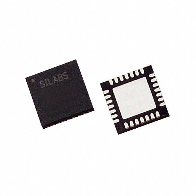
ICGOO电子元器件商城为您提供CP2201-GM由Silicon Laboratories设计生产,在icgoo商城现货销售,并且可以通过原厂、代理商等渠道进行代购。 CP2201-GM价格参考。Silicon LaboratoriesCP2201-GM封装/规格:接口 - 控制器, 以太网 控制器 10/100/1000 Base-T PHY 并联 接口 28-QFN(5x5)。您可以下载CP2201-GM参考资料、Datasheet数据手册功能说明书,资料中有CP2201-GM 详细功能的应用电路图电压和使用方法及教程。
Silicon Labs 的 CP2201-GM 是一款高度集成的 USB 至以太网控制器,主要应用于需要将 USB 接口转换为以太网连接的场景。该芯片内置 USB 2.0 控制器和以太网 MAC/PHY,支持 10/100Mbps 以太网速率,适用于工业控制、嵌入式系统、测试设备、网络接入设备等场景。

CP2201-GM 常用于以下应用场景:

1. 工业自动化设备:为不具备以太网接口的工业设备提供联网能力,实现远程监控与数据传输。
2. 嵌入式系统开发:作为系统与外部网络通信的桥梁,简化设计并提高开发效率。
3. USB转网口适配器:用于扩展主机设备的网络连接功能,如便携式路由器或网络故障排查工具。
4. 测试与测量仪器:实现仪器与网络之间的高速数据传输,便于远程控制与数据采集。
5. 智能家电与物联网设备:为设备提供稳定可靠的网络连接,支持 IoT 应用中的通信需求。

其优势在于集成度高、兼容性强、功耗低,适合对空间和性能有要求的应用场合。
| 参数 | 数值 |
| 产品目录 | 集成电路 (IC)半导体 |
| 描述 | IC ETH CTRLR SNGL-CHIP 28QFN以太网 IC Ethernet Controller |
| 产品分类 | |
| 品牌 | Silicon Laboratories IncSilicon Labs |
| 产品手册 | |
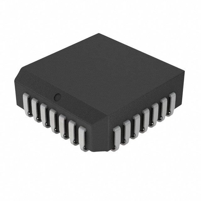
| 产品图片 |
|
| rohs | 符合RoHS无铅 / 符合限制有害物质指令(RoHS)规范要求 |
| 产品系列 | 通信及网络 IC,以太网 IC,Silicon Labs CP2201-GM- |
| 数据手册 | |
| 产品型号 | CP2201-GMCP2201-GM |
| 产品 | Ethernet Controllers |
| 产品目录页面 | |
| 产品种类 | 以太网 IC |
| 以太网连接类型 | 1000Base-T, 100Base-T, 10Base-T |
| 供应商器件封装 | 28-QFN(5x5) |
| 其它名称 | 336-1313 |
| 功能 | 控制器 |
| 包装 | 管件 |
| 协议 | 以太网 |
| 单位重量 | 67.750 mg |
| 商标 | Silicon Labs |
| 安装风格 | SMD/SMT |
| 封装 | Tube |
| 封装/外壳 | 28-VFQFN 裸露焊盘 |
| 封装/箱体 | QFN-28 |
| 工作温度 | -40°C ~ 85°C |
| 工厂包装数量 | 73 |
| 接口 | 并联 |
| 支持标准 | 802.3 |
| 数据速率 | 10 Mbps, 100 Mbps, 1000 Mbps |
| 最大工作温度 | + 85 C |
| 最小工作温度 | - 40 C |
| 标准 | 10/100/1000 Base-T PHY |
| 标准包装 | 73 |
| 电压-电源 | 3.1 V ~ 3.6 V |
| 电流-电源 | 75mA |
| 系列 | CP2201 |
| 配用 | /product-detail/zh/POE-VOICE-RD/336-1326-ND/1201223/product-detail/zh/CP2201EK/336-1316-ND/1013433 |


- 商务部:美国ITC正式对集成电路等产品启动337调查
- 曝三星4nm工艺存在良率问题 高通将骁龙8 Gen1或转产台积电
- 太阳诱电将投资9.5亿元在常州建新厂生产MLCC 预计2023年完工
- 英特尔发布欧洲新工厂建设计划 深化IDM 2.0 战略
- 台积电先进制程称霸业界 有大客户加持明年业绩稳了
- 达到5530亿美元!SIA预计今年全球半导体销售额将创下新高
- 英特尔拟将自动驾驶子公司Mobileye上市 估值或超500亿美元
- 三星加码芯片和SET,合并消费电子和移动部门,撤换高东真等 CEO
- 三星电子宣布重大人事变动 还合并消费电子和移动部门
- 海关总署:前11个月进口集成电路产品价值2.52万亿元 增长14.8%


PDF Datasheet 数据手册内容提取
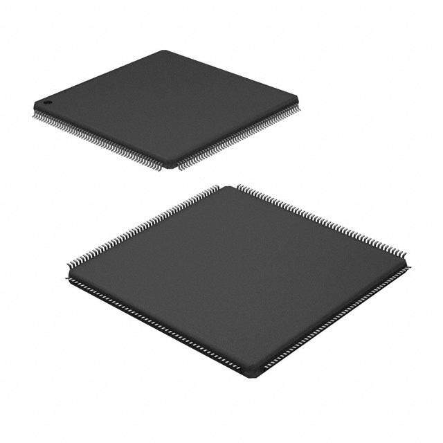
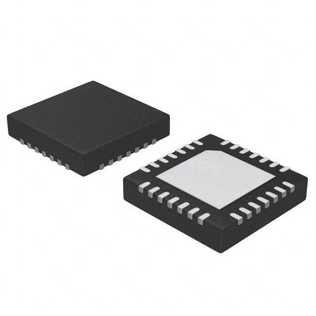
CP2200/1 SINGLE-CHIP ETHERNET CONTROLLER Ethernet Controller Software Support Integrated IEEE 802.3 MAC and 10BASE-T PHY Royalty-free TCP/IP stack with device drivers Fully compatible with 100/1000BASE-T networks TCP/IP Stack Configuration Wizard Full/Half duplex with auto-negotiation Hardware diagnostic software and example code Automatic polarity detection and correction Example Applications Automatic retransmission on collision Remote sensing and monitoring Automatic padding and CRC generation Inventory management Supports broadcast and multi-cast MAC addressing VoIP phone adapters Parallel Host Interface (30Mbps Transfer Rate) Point-of-sale devices 8-bit multiplexed or non-multiplexed mode Network clocks Only 11 I/O pins required in multiplexed mode Embedded Web Server Intel® or Motorola® Bus Format Remote Ethernet-to-UART bridge Interrupt on received packets and Wake-on-LAN Supply Voltage 8kB Flash Memory 3.1 to 3.6V 8192 bytes ISP non-volatile memory Package Factory pre-programmed unique 48-bit MAC Address Pb-free 48-pin TQFP (9x9mm footprint) No external EEPROM required Pb-free 28-pin QFN (5x5mm footprint) Other Features Ordering Part Number LED output drivers (Link/Activity) CP2200-GQ (48-pin) Dedicated 2kB RAM transmit buffer and 4kB RAM CP2201-GM (28-pin) receive FIFO buffer Power-on Reset Temperature Range: –40 to +85°C 5V Tolerant I/O 20 MHz XTAL CP2200 LED 8 kB Clock Control Flash us ACT B 2 kB LED el Host Tx Buffer TX+/TX- all Interface ar Ethernet Ethernet P RJ-45 MAC PHY 4 kB RX+/RX- Rx FIFO LINK LED Figure 1. Example System Diagram Rev. 1.0 5/07 Copyright © 2007 by Silicon Laboratories CP2200/1
CP2200/1 2 Rev. 1.0
CP2200/1 TABLE OF CONTENTS Section Page 1. System Overview . . . . . . . . . . . . . . . . . . . . . . . . . . . . . . . . . . . . . . . . . . . . . . . . . . . . . . . . .5 2. Typical Connection Diagram . . . . . . . . . . . . . . . . . . . . . . . . . . . . . . . . . . . . . . . . . . . . . . . .6 3. Absolute Maximum Ratings . . . . . . . . . . . . . . . . . . . . . . . . . . . . . . . . . . . . . . . . . . . . . . . .8 4. Electrical Characteristics . . . . . . . . . . . . . . . . . . . . . . . . . . . . . . . . . . . . . . . . . . . . . . . . . .9 5. Pinout and Package Definitions . . . . . . . . . . . . . . . . . . . . . . . . . . . . . . . . . . . . . . . . . . . .10 6. Functional Description . . . . . . . . . . . . . . . . . . . . . . . . . . . . . . . . . . . . . . . . . . . . . . . . . . .18 6.1. Overview . . . . . . . . . . . . . . . . . . . . . . . . . . . . . . . . . . . . . . . . . . . . . . . . . . . . . . . . . .18 6.2. Reset Initialization . . . . . . . . . . . . . . . . . . . . . . . . . . . . . . . . . . . . . . . . . . . . . . . . . . .18 6.3. Interrupt Request Signal . . . . . . . . . . . . . . . . . . . . . . . . . . . . . . . . . . . . . . . . . . . . . .18 6.4. Clocking Options . . . . . . . . . . . . . . . . . . . . . . . . . . . . . . . . . . . . . . . . . . . . . . . . . . . .19 6.5. LED Control . . . . . . . . . . . . . . . . . . . . . . . . . . . . . . . . . . . . . . . . . . . . . . . . . . . . . . . .21 6.6. Sending and Receiving Packets . . . . . . . . . . . . . . . . . . . . . . . . . . . . . . . . . . . . . . . .22 7. Internal Memory and Registers . . . . . . . . . . . . . . . . . . . . . . . . . . . . . . . . . . . . . . . . . . . . .23 7.1. Random Access to RAM Transmit and Receive Buffers . . . . . . . . . . . . . . . . . . . . . .23 7.2. Internal Registers . . . . . . . . . . . . . . . . . . . . . . . . . . . . . . . . . . . . . . . . . . . . . . . . . . .25 8. Interrupt Sources . . . . . . . . . . . . . . . . . . . . . . . . . . . . . . . . . . . . . . . . . . . . . . . . . . . . . . . .30 9. Reset Sources . . . . . . . . . . . . . . . . . . . . . . . . . . . . . . . . . . . . . . . . . . . . . . . . . . . . . . . . . .37 9.1. Power-On Reset . . . . . . . . . . . . . . . . . . . . . . . . . . . . . . . . . . . . . . . . . . . . . . . . . . . .38 9.2. Power-fail . . . . . . . . . . . . . . . . . . . . . . . . . . . . . . . . . . . . . . . . . . . . . . . . . . . . . . . . .39 9.3. Oscillator-Fail Reset . . . . . . . . . . . . . . . . . . . . . . . . . . . . . . . . . . . . . . . . . . . . . . . . .39 9.4. External Pin Reset . . . . . . . . . . . . . . . . . . . . . . . . . . . . . . . . . . . . . . . . . . . . . . . . . .39 9.5. Software Reset . . . . . . . . . . . . . . . . . . . . . . . . . . . . . . . . . . . . . . . . . . . . . . . . . . . . .40 9.6. Determining the Source of the Last Reset . . . . . . . . . . . . . . . . . . . . . . . . . . . . . . . .41 9.7. De-Selecting Interrupt Sources . . . . . . . . . . . . . . . . . . . . . . . . . . . . . . . . . . . . . . . . .42 10. Power Modes . . . . . . . . . . . . . . . . . . . . . . . . . . . . . . . . . . . . . . . . . . . . . . . . . . . . . . . . . .43 10.1. Normal Mode . . . . . . . . . . . . . . . . . . . . . . . . . . . . . . . . . . . . . . . . . . . . . . . . . . . . . .44 10.2. Link Detection Mode . . . . . . . . . . . . . . . . . . . . . . . . . . . . . . . . . . . . . . . . . . . . . . . .44 10.3. Memory Mode . . . . . . . . . . . . . . . . . . . . . . . . . . . . . . . . . . . . . . . . . . . . . . . . . . . . .44 10.4. Shutdown Mode . . . . . . . . . . . . . . . . . . . . . . . . . . . . . . . . . . . . . . . . . . . . . . . . . . .44 10.5. Disabling Secondary Device Functions . . . . . . . . . . . . . . . . . . . . . . . . . . . . . . . . . .45 11. Transmit Interface . . . . . . . . . . . . . . . . . . . . . . . . . . . . . . . . . . . . . . . . . . . . . . . . . . . . . .47 11.1. Overview . . . . . . . . . . . . . . . . . . . . . . . . . . . . . . . . . . . . . . . . . . . . . . . . . . . . . . . . .47 11.2. Transmitting a Packet . . . . . . . . . . . . . . . . . . . . . . . . . . . . . . . . . . . . . . . . . . . . . . .48 11.3. Overriding Transmit Configuration Options . . . . . . . . . . . . . . . . . . . . . . . . . . . . . . .48 11.4. Transmit Buffer and AutoWrite Interface . . . . . . . . . . . . . . . . . . . . . . . . . . . . . . . . .48 11.5. Transmit Status and Control Registers . . . . . . . . . . . . . . . . . . . . . . . . . . . . . . . . . .49 12. Receive Interface . . . . . . . . . . . . . . . . . . . . . . . . . . . . . . . . . . . . . . . . . . . . . . . . . . . . . . .58 12.1. Overview . . . . . . . . . . . . . . . . . . . . . . . . . . . . . . . . . . . . . . . . . . . . . . . . . . . . . . . . .58 12.2. Reading a Packet Using the Autoread Interface . . . . . . . . . . . . . . . . . . . . . . . . . . .58 12.3. Timing and Buffer Overflow Considerations . . . . . . . . . . . . . . . . . . . . . . . . . . . . . .58 12.4. Initializing the Receive Buffer, Filter and Hash Table . . . . . . . . . . . . . . . . . . . . . . .59 Rev. 1.0 3
CP2200/1 12.5. Receive Status and Control Registers . . . . . . . . . . . . . . . . . . . . . . . . . . . . . . . . . .60 12.6. Advanced Receive Buffer Operation . . . . . . . . . . . . . . . . . . . . . . . . . . . . . . . . . . . .66 12.7. Receive Buffer Advanced Status and Control Registers . . . . . . . . . . . . . . . . . . . . .67 13. Flash Memory . . . . . . . . . . . . . . . . . . . . . . . . . . . . . . . . . . . . . . . . . . . . . . . . . . . . . . . . . .73 13.1. Programming the Flash Memory . . . . . . . . . . . . . . . . . . . . . . . . . . . . . . . . . . . . . . .73 13.2. Reading the Flash Memory . . . . . . . . . . . . . . . . . . . . . . . . . . . . . . . . . . . . . . . . . . .74 13.3. Flash Access Registers . . . . . . . . . . . . . . . . . . . . . . . . . . . . . . . . . . . . . . . . . . . . . .75 14. Media Access Controller (MAC) . . . . . . . . . . . . . . . . . . . . . . . . . . . . . . . . . . . . . . . . . . .78 14.1. Initializing the MAC . . . . . . . . . . . . . . . . . . . . . . . . . . . . . . . . . . . . . . . . . . . . . . . . .78 14.2. Accessing the Indirect MAC Registers . . . . . . . . . . . . . . . . . . . . . . . . . . . . . . . . . .78 14.3. Indirect MAC Register Descriptions . . . . . . . . . . . . . . . . . . . . . . . . . . . . . . . . . . . .80 15. Physical Layer (PHY) . . . . . . . . . . . . . . . . . . . . . . . . . . . . . . . . . . . . . . . . . . . . . . . . . . . .88 15.1. Auto-Negotiation and Duplex Mode . . . . . . . . . . . . . . . . . . . . . . . . . . . . . . . . . . . .88 15.2. Auto-Negotiation Synchronization . . . . . . . . . . . . . . . . . . . . . . . . . . . . . . . . . . . . . .88 15.3. Loopback Mode . . . . . . . . . . . . . . . . . . . . . . . . . . . . . . . . . . . . . . . . . . . . . . . . . . . .89 15.4. Link Integrity Function . . . . . . . . . . . . . . . . . . . . . . . . . . . . . . . . . . . . . . . . . . . . . . .89 15.5. Receiver Smart Squelch and Automatic Polarity Correction . . . . . . . . . . . . . . . . . .89 15.6. Transmitter Jabber Function . . . . . . . . . . . . . . . . . . . . . . . . . . . . . . . . . . . . . . . . . .89 15.7. Initializing the Physical Layer . . . . . . . . . . . . . . . . . . . . . . . . . . . . . . . . . . . . . . . . .90 16. Parallel Interface . . . . . . . . . . . . . . . . . . . . . . . . . . . . . . . . . . . . . . . . . . . . . . . . . . . . . . . .96 16.1. Non-Multiplexed Intel Format . . . . . . . . . . . . . . . . . . . . . . . . . . . . . . . . . . . . . . . . .96 16.2. Multiplexed Intel Format . . . . . . . . . . . . . . . . . . . . . . . . . . . . . . . . . . . . . . . . . . . . .98 16.3. Non-Multiplexed Motorola Format . . . . . . . . . . . . . . . . . . . . . . . . . . . . . . . . . . . . .100 16.4. Multiplexed Motorola Format . . . . . . . . . . . . . . . . . . . . . . . . . . . . . . . . . . . . . . . . .102 17. Revision-Specific Behavior . . . . . . . . . . . . . . . . . . . . . . . . . . . . . . . . . . . . . . . . . . . . . .104 17.1. Revision Identification . . . . . . . . . . . . . . . . . . . . . . . . . . . . . . . . . . . . . . . . . . . . . .104 17.2. MAC Address Filtering . . . . . . . . . . . . . . . . . . . . . . . . . . . . . . . . . . . . . . . . . . . . .105 Document Change List . . . . . . . . . . . . . . . . . . . . . . . . . . . . . . . . . . . . . . . . . . . . . . . . . . . .106 4 Rev. 1.0
CP2200/1 1. System Overview The CP2200/1 is a single-chip Ethernet controller containing an integrated IEEE802.3 Ethernet Media Access Controller (MAC), 10BASE-T Physical Layer (PHY), and 8kB Non-Volatile Flash Memory available in a compact 5x5mm QFN-28 package (sometimes called “MLF” or “MLP”) and a 48-pin TQFP package. The CP2200/1 can add Ethernet connectivity to any microcontroller or host processor with 11 or more Port I/O pins. The 8-bit parallel interface bus supports both Intel and Motorola bus formats in multiplexed and non-multiplexed mode. The data transfer rate in non-multiplexed mode can exceed 30Mbps. The on-chip Flash memory may be used to store user constants, web server content, or as general purpose non- volatile memory. The Flash is factory preprogrammed with a unique 48-bit MAC address stored in the last six memory locations. Having a unique MAC address stored in the CP2200/1 often removes the serialization step from the product manufacturing process of most embedded systems. The CP2200/1 has four power modes with varying levels of functionality that allow the host processor to manage the overall system power consumption. The optional interrupt pin also allows the host to enter a “sleep” mode and awaken when a packet is received or when the CP2200/1 is plugged into a network. Auto-negotiation allows the device to automatically detect the most efficient duplex mode (half/full duplex) supported by the network. The Ethernet Development Kit (Ethernet-DK) bundles a C8051F120 MCU Target Board, CP2200 Ethernet Development Board (AB4), the Silicon Laboratories IDE, all necessary debug hardware, and a TCP/IP Configuration Wizard. The Ethernet Development Kit includes all hardware, software, and examples necessary to design an embedded system using the CP2200. The CP2200 Ethernet Development Board is also compatible with the C8051F020TB and C8051F340TB. Individual target boards may be purchased online by visiting www.silabs.com. Rev. 1.0 5
CP2200/1 2. Typical Connection Diagram Figure2 and Figure3 show typical connection diagrams for the 48-pin CP2200 and 28-pin CP2201. +3VD 0.1 uF 0.1 uF 0.1 uF 10 uF +3VD +12 4.7 k VDD XTAL1 ADD RST 20 MHz 10 M VV XTAL2 MUXEN 22 pF 22 pF MOTEN Integrated RJ-45 Jack MCU CP2200 LINK ACT ACT LINK A15 Optional CS 8 A[7:0] A[7:0] 8 D[7:0] D[7:0] 8 1:2.5 TX+ TXP RD RD 0.001 uF RJ-45 WR WR 0.001 uF 1 TX– TXN 2 8 TCT 3 4 0.1 uF 5 INT Optional INT 1:1 6 RX+ RXP 7 100 8 DGND1 RX– RXN DGND2 RCT 0.1 uF GND AGND Chassis Ground Note: The CP220x should be placed within 1 inch of the transformer for optimal performance. Figure 2. Typical Connection Diagram (Non-Multiplexed) 6 Rev. 1.0
CP2200/1 +3VD 0.1 uF 0.1 uF 0.1 uF 10 uF +3VD V+D1D2 4.7 k XTAL1 ADD RST 20 MHz 10 M VV XTAL2 22 pF 22 pF MOTEN MCU CS CP2201 LA LINK/ACTIVITY 8 AD[7:0] AD[7:0] Integrated RJ-45 Jack 8 1:2.5 TX+ TXP RD RD 0.001 uF RJ-45 WR WR 0.001 uF 1 TX– TXN 2 ALE ALE 8 TCT 3 4 INT Optional INT 0.1 uF 5 1:1 6 RX+ RXP 7 DGND1 100 8 RX– RXN DGND2 RCT GND AGND 0.1 uF Chassis Ground Note: The CP220x should be placed within 1 inch of the transformer for optimal performance. Figure 3.Typical Connection Diagram (Multiplexed) Rev. 1.0 7
CP2200/1 3. Absolute Maximum Ratings Table 1. Absolute Maximum Ratings Parameter Conditions Min Typ Max Units Ambient temperature under bias –55 — 125 °C Storage Temperature –65 — 150 °C Voltage on any I/O Pin or RST with respect to GND –0.3 — 5.8 V Voltage on V with respect to GND –0.3 — 4.2 V DD Maximum Total current through V and GND — — 500 mA DD Maximum output current sunk by RST or any I/O pin — — 100 mA Note: Stresses above those listed may cause permanent damage to the device. This is a stress rating only, and functional operation of the devices at or exceeding the conditions in the operation listings of this specification is not implied. Exposure to maximum rating conditions for extended periods may affect device reliability. 8 Rev. 1.0
CP2200/1 4. Electrical Characteristics Table 2. Global DC Electrical Characteristics V =3.1 to 3.6V, –40 to +85 °C unless otherwise specified. DD Parameter Conditions Min Typ Max Units Supply Voltage 3.1 3.3 3.6 V Supply Current in Normal Mode (Transmitting) V =3.3 V — 75 155 mA DD Supply Current in Normal Mode (No Network V =3.3 V — 60 — mA DD Traffic) Supply Current with Transmitter and Receiver V =3.3 V — 47 — mA DD Disabled (Memory Mode) Supply Current in Reset V = 3.3V — 15 — mA DD Supply Current in Shutdown Mode V =3.3 V — 6.5 — mA DD Specified Operating Temperature Range –40 — +85 °C Table 3. Digital I/O DC Electrical Characteristics V =3.1 to 3.6V, –40 to +85°C unless otherwise specified. DD Parameters Conditions Min Typ Max UNITS Output High Voltage (V ) I =–3mA V – 0.7 — — V OH OH DD I =–10µA V – 0.1 — — OH DD I =–10mA — V – 0.8 — OH DD Output Low Voltage (V ) I =8.5mA — — 0.6 V OL OL I =10µA — — 0.1 OL I =25mA — 1.0 — OL Input High Voltage (V ) 2.0 — — V IH Input Low Voltage (V ) — — 0.8 V IL Input Leakage Current — 25 50 µA Rev. 1.0 9
CP2200/1 5. Pinout and Package Definitions Table 4. CP2200/1 Pin Definitions Name Pin Numbers Type Description 48-pin 28-pin AV+ 5 3 Power In 3.1–3.6V Analog Power Supply Voltage Input. AGND 4 2 Analog Ground V 13 8 Power In 3.1–3.6V Digital Power Supply Voltage Input. DD1 DGND1 14 9 Digital Ground V 30 19 Power In 3.1–3.6V Digital Power Supply Voltage Input. DD2 DGND2 31 20 Digital Ground RST 15 10 D I/O Device Reset. Open-drain output of internal POR and V monitor. DD An external source can initiate a system reset by driving this pin low for at least 15µs. LINK 3* — D Out Link LED. Push-pull output driven high when valid 10BASE-T link pulses are detected (Link Good) and driven low when valid 10BASE-T link pulses are not detected (Link Fail). ACT 2* — D Out Activity LED. Push-pull output driven high for 50ms when any packet is transmitted or received and driven low all other times. LA — 1* D Out Link or Activity LED. Push-pull output driven high when valid link pulses are detected (Link Good) and driven low otherwise (Link Fail). The output is toggled for each packet transmitted or received, then returns to its original state after 50ms. XTAL1 46 28 A In Crystal Input. This pin is the return for the external oscillator driver. This pin can be overdriven by an external CMOS clock. XTAL2 45* 27* A Out Crystal Output. This pin is the excitation driver for a quartz crystal. TX+ 9 6 A Out 10BASE-T Transmit, Differential Output (Positive). TX– 10 7 A Out 10BASE-T Transmit, Differential Output (Negative). RX+ 7 5 A In 10BASE-T Receive, Differential Input (Positive). RX– 6 4 A In 10BASE-T Receive, Differential Input (Negative). MOTEN 43 26 D In Motorola Bus Format Enable. This pin should be tied directly to V DD for Motorola bus format or directly to GND for Intel bus format. MUXEN 44 — D In Multiplexed Bus Enable. This pin should be tied directly to V for DD multiplexed bus mode or directly to GND for non-multiplexed bus mode. INT 42 25 D Out Interrupt Service Request. This pin provides notification to the host. *Note: Pins can be left unconnected when not used. 10 Rev. 1.0
CP2200/1 Table 4. CP2200/1 Pin Definitions (Continued) Name Pin Numbers Type Description 48-pin 28-pin CS 41 24 D In Device Chip Select. RD/(DS) 39 22 D In Read Strobe (Intel Mode) or Data Strobe (Motorola Mode) WR/(R/W) 40 23 D In Write Strobe (Intel Mode) or Read/Write Strobe (Motorola Mode) D0/AD0 16 11 D I/O Bit 0, Non-Multiplexed Data Bus or Multiplexed Address/Data Bus D1/AD1 17 12 D I/O Bit 1, Non-Multiplexed Data Bus or Multiplexed Address/Data Bus D2/AD2 18 13 D I/O Bit 2, Non-Multiplexed Data Bus or Multiplexed Address/Data Bus D3/AD3 19 14 D I/O Bit 3, Non-Multiplexed Data Bus or Multiplexed Address/Data Bus D4/AD4 20 15 D I/O Bit 4, Non-Multiplexed Data Bus or Multiplexed Address/Data Bus D5/AD5 21 16 D I/O Bit 5, Non-Multiplexed Data Bus or Multiplexed Address/Data Bus D6/AD6 22 17 D I/O Bit 6, Non-Multiplexed Data Bus or Multiplexed Address/Data Bus D7/AD7 23 18 D I/O Bit 7, Non-Multiplexed Data Bus or Multiplexed Address/Data Bus A0 27* — D In Bit 0, Non-Multiplexed Address Bus A1 28* — D In Bit 1, Non-Multiplexed Address Bus A2 29* — D In Bit 2, Non-Multiplexed Address Bus A3/ALE/(AS) 32 — D In Bit 3, Non-Multiplexed Address Bus ALE Strobe (Multiplexed Intel Mode) Address Strobe (Multiplexed Motorola Mode) ALE/(AS) — 21 D In ALE Strobe (Intel Mode) Address Strobe (Motorola Mode) A4 33* — D In Bit 4, Parallel Interface Non-Multiplexed Address Bus A5 34* — D In Bit 5, Parallel Interface Non-Multiplexed Address Bus A6 37* — D In Bit 6, Parallel Interface Non-Multiplexed Address Bus A7 38* — D In Bit 7, Parallel Interface Non-Multiplexed Address Bus NC 1, 8, — These pins should be left unconnected or tied to V . DD 11,12 24–26 35,36 47, 48 *Note: Pins can be left unconnected when not used. Rev. 1.0 11
CP2200/1 ) W NC NC XTAL1 XTAL2 MUXEN MOTEN NT CS WR/(R/ RD/(DS) A7 A6 I 8 7 6 5 4 3 2 1 0 9 8 7 4 4 4 4 4 4 4 4 4 3 3 3 NC 1 36 NC ACT 2 35 NC LINK 3 34 A5 AGND 4 33 A4 AV+ 5 32 A3/ALE/(AS) CP2200 RX- 6 31 DGND2 Top View RX+ 7 30 VDD2 NC 8 29 A2 TX+ 9 28 A1 TX- 10 27 A0 NC 11 26 NC NC 12 25 NC 3 4 5 6 7 8 9 0 1 2 3 4 1 1 1 1 1 1 1 2 2 2 2 2 1 1 T 0 1 2 3 4 5 6 7 C D D S D D D D D D D D N D N R A A A A A A A A V G 0/ 1/ 2/ 3/ 4/ 5/ 6/ 7/ D D D D D D D D D Figure 4. 48-pin TQFP Pinout Diagram 12 Rev. 1.0
CP2200/1 D D1 Table 5. TQFP-48 Package Dimensions MM Min Typ Max A — — 1.20 A1 0.05 — 0.15 E1 E A2 0.95 1.00 1.05 b 0.17 0.22 0.27 D — 9.00 — D1 — 7.00 — E — 9.00 — e — 0.50 — E1 — 7.00 — 48 PIN 1 IDENTIFIER 1 e A2 A b A1 Figure 5.48-pin TQFP Package Dimensions Rev. 1.0 13
CP2200/1 ) W XTAL1 XTAL2 MOTEN NT CS WR/(R/ RD/(DS) I 8 7 6 5 4 3 2 GND 2 2 2 2 2 2 2 LA 1 21 ALE/(AS) AGND 2 20 DGND2 AV+ 3 19 VDD2 CP2201 RX- 4 18 AD7 Top View RX+ 5 17 AD6 TX+ 6 16 AD5 GND TX- 7 15 AD4 8 9 10 11 12 13 14 1 1 T 0 1 2 3 D D S D D D D D N R A A A A V G D Figure 6.QFN-28 Pinout Diagram (Top View) 14 Rev. 1.0
CP2200/1 Bottom View 8 9 10 11 12 13 14 Table 6. QFN-28 Package Dimensions L MM 7 15 Min Typ Max A 0.80 0.90 1.00 6 16 D2 A1 0 0.02 0.05 b 5 D2 17 A2 0 0.65 1.00 2 A3 — 0.25 — e 4 E2 R 18 6 x E b 0.18 0.23 0.30 e D — 5.00 — 3 19 2 D2 2.90 3.15 3.35 E 2 2 20 E — 5.00 — E2 2.90 3.15 3.35 1 DETAIL 1 21 e — 0.5 — L 0.45 0.55 0.65 N — 28 — 8 7 6 5 4 3 2 2 2 2 2 2 2 2 ND — 7 — NE — 7 — 6 x e R 0.09 — — D Side View AA — 0.435 — BB — 0.435 — CC — 0.18 — 2 A A DD — 0.18 — e 3 1 A A DETAIL 1 AA B B CC D D Figure 7. QFN-28 Package Drawing Rev. 1.0 15
CP2200/1 Top View m m m m 0.85 mm m m m m 0.50 0.20 0.20 0.30 m m m 0.50 mm 0.50 0.10 m m m 0.20 mm 0.35 Optional GND Connection b D2 D L E2 e 0.20 mm 0.30 mm 0.50 mm 0.35 mm 0.85 mm 0.10 mm E Figure8. Typical QFN-28 Landing Diagram 16 Rev. 1.0
CP2200/1 Top View m m m m 0.85 mm m m m m 0.50 0.20 0.20 0.30 m m m 0.50 mm 0.50 0.10 m m m 0.20 mm 0.60 mm 0.35 0.60 mm 0.70 mm 0.30 mm b 0.20 mm 0.40 mm D2 D L e E2 0.20 mm 0.30 mm 0.50 mm 0.35 mm 0.85 mm 0.10 mm E Figure 9.Typical QFN-28 Solder Paste Diagram Rev. 1.0 17
CP2200/1 6. Functional Description 6.1. Overview In most systems, the CP2200/1 is used for transmitting and receiving Ethernet packets, non-volatile data storage, and controlling Link and Activity LEDs. The device is controlled using direct and indirect internal registers accessible through the parallel host interface. All digital pins on the device are 5V tolerant. 6.2. Reset Initialization After every CP2200/1 reset, the following initialization procedure is recommended to ensure proper device operation: Step 1: Wait for the reset pin to rise. This step takes the longest during a power-on reset. Step 2: Wait for Oscillator Initialization to complete. The host processor will receive notification through the interrupt request signal once the oscillator has stabilized. Step 3: Wait for Self Initialization to complete. The INT0 interrupt status register on page31 should be checked to determine when Self Initialization completes. Step 4: Disable interrupts (using INT0EN and INT1EN on page33 and page36) for events that will not be monitored or handled by the host processor. By default, all interrupts are enabled after every reset. Step 5: Initialize the physical layer. See “15.7. Initializing the Physical Layer” on page90 for a detailed physical layer initialization procedure. Step 6: Enable the desired Activity, Link, or Activity/Link LEDs using the IOPWR register on page45. Step 7: Initialize the media access controller (MAC). See “14.1. Initializing the MAC” on page78 for a detailed MAC initialization procedure. Step 8: Configure the receive filter. See “12.4. Initializing the Receive Buffer, Filter and Hash Table” on page59 for a detailed initialization procedure. Step 9: The CP2200/1 is ready to transmit and receive packets. 6.3. Interrupt Request Signal The CP2200/1 has an interrupt request signal (INT) that can be used to notify the host processor of pending interrupts. The INT signal is asserted upon detection of any enabled interrupt event. Host processors that cannot dedicate a port pin to the INT signal can periodically poll the interrupt status registers to see if any interrupt generating events have occurred. If the /INT signal is not used, pending interrupts such a Receive FIFO Full must still be serviced. The 14 interrupt sources are listed below. Interrupts are enabled on reset and can be disabled by software. Pending interrupts can be cleared (allowing the INT signal to de-assert) by reading the self-clearing interrupt registers. See “8. Interrupt Sources” on page30 for a complete description of the CP2200/1 interrupts. End of Packet Reached Packet Received Receive FIFO Empty “Wake-on-LAN” Wakeup Event Receive FIFO Full Link Status Changed Oscillator Initialization Complete Jabber Detected Self Initialization Complete Auto-Negotiation Failed Flash Write/Erase Complete Remote Fault Notification Packet Transmitted Auto-Negotiation Complete 18 Rev. 1.0
CP2200/1 6.4. Clocking Options The CP2200/1 can be clocked from an external parallel-mode crystal oscillator or CMOS clock. Figure10 and Figure11 show typical connections for both clock source types. If a crystal oscillator is chosen to clock the device, the crystal is started once the device is released from reset and remains on until the device reenters the reset state or loses power. XTAL1 20 MHz 10 M XTAL2 Figure 10. Crystal Oscillator Example Important note on external crystals: Crystal oscillator circuits are quite sensitive to PCB layout. The crystal should be placed as close as possible to the XTAL pins on the device. The traces should be as short as possible and shielded with a ground plane from any other traces that could introduce noise or interference. 20 MHz XTAL1 CMOS Clock XTAL2 No Connect Figure11. External CMOS Clock Example Table7 lists the clocking requirements of the CP2200/1 when using a crystal oscillator or CMOS clock. Table8 shows the electrical characteristics of the XTAL1 pin. These characteristics are useful when selecting an external CMOS clock. Rev. 1.0 19
CP2200/1 Table 7. Clocking Requirements V =3.1 to 3.6V, –40 to +85°C unless otherwise specified. DD Parameters Conditions Min Typ Max UNITS Frequency — 20 — MHz Frequency Error — — 50 ppm Duty Cycle 45 50 55 % Table 8. Input Clock Pin (XTAL1) DC Electrical Characteristics V =3.1 to 3.6V, –40 to +85°C unless otherwise specified. DD Parameters Conditions Min Typ Max UNITS XTAL1 Input Low Voltage — — 0.7 V XTAL1 Input High Voltage 2.0 — — V 20 Rev. 1.0
CP2200/1 6.5. LED Control The CP2200/1 can be used to control link status and activity LEDs. The CP2200 (48-pin TQFP) has two push-pull LED drivers that can source up to 10mA each. The CP2201 (28-pin QFN) has a single push-pull LED driver that turns the LED on or off based on the link status and blinks the LED when activity is detected on a good link. Table9 shows the function of the LED signals available on the CP2200/1. Table 9. LED Control Signals Signal Device Description LINK CP2200 Asserted when valid link pulses are detected. ACT CP2200 Asserted for 50ms for each packet transmitted or received. LA CP2201 Asserted when valid link pulses are detected and toggled for 50ms for each packet transmitted or received. Figure12 shows a typical LED connection for the CP2200. The CP2201 uses an identical connection for the LA (link/activity) pin. The LED drivers are enabled and disabled using the IOPWR register on page45. LINK ACT Figure 12. LED Control Example (CP2200) Rev. 1.0 21
CP2200/1 6.6. Sending and Receiving Packets After reset initialization is complete, the CP2200/1 is ready to send and receive packets. Packets are sent by loading data into the transmit buffer using the AutoWrite register and writing ‘1’ to TXGO. See “11.2. Transmitting a Packet” on page48 for detailed information on how to transmit a packet using the transmit interface. A Packet Transmitted interrupt will be generated once transmission is complete. Packet reception occurs automatically when reception is enabled in the MAC and the receive buffer is not full. Once a packet is received, the host processor is notified by generating a Packet Received interrupt. The host may read the packet using the AutoRead interface. See “12.2. Reading a Packet Using the Autoread Interface” on page58 and “12.4. Initializing the Receive Buffer, Filter and Hash Table” on page59 for additional information on using and initializing the receive interface. 22 Rev. 1.0
CP2200/1 7. Internal Memory and Registers The CP2200/1 is controlled through direct and indirect registers accessible through the parallel host interface. The host interface provides an 8-bit address space, of which there are 114 valid direct register locations (see Table11 on page25). All remaining addresses in the memory space are reserved and should not be read or written. The direct registers provide access to the RAM buffers, Flash memory, indirect MAC configuration registers, and other status and control registers for various device functions. Figure13 shows the RAM and Flash memory organization. The transmit and receive RAM buffers share the same address space and are both accessed using the RAMADDRH:RAMADDRL pointer. Each of the buffers has a dedicated data register. The Flash memory has a separate address space and a dedicated address pointer and data register. See “13. Flash Memory” on page73 for detailed information on how to read and write to Flash. Transmit Buffer (2K) 0x0000 – 0x07FF Receive Buffer (4K) 0x0000 – 0x0FFF Flash Memory (8K) 0x0000 – 0x1FFF RAMADDRH:RAMADDRL FLASHADDRH:FLASHADDRL Figure 13. RAM Buffers and Flash Memory Organization 7.1. Random Access to RAM Transmit and Receive Buffers The most common and most efficient methods for accessing the transmit and receive buffers are the AutoWrite and AutoRead interfaces. These interfaces allow entire packets to be written or read at a time. In very few cases, the transmit and receive buffers may need to be accessed randomly. An example of this is a system in which a specific byte in the packet is checked to determine whether to read the packet or discard it. The following procedure can be used to read or write data to either RAM buffer: Step 1: Write the address of the target byte to RAMADDRH:RAMADDRL. Step 2: Transmit Buffer: Read or write 8-bit data to RAMTXDATA to read or write from the target byte in the transmit buffer. Receive Buffer: Read or write 8-bit data to RAMRXDATA to read or write from the target byte in the receive buffer. Note: Reads and writes of the RAM buffers using the random access method are independent of the AutoRead and AutoWrite interfaces. Each of the interfaces has a dedicated set of address and data registers. See “11.2. Transmitting a Packet” on page48 and “12.2. Reading a Packet Using the Autoread Interface” on page58 for additional information about the AutoRead and AutoWrite interfaces. Rev. 1.0 23
CP2200/1 Register 1. RAMADDRH: RAM Address Pointer High Byte R/W R/W R/W R/W R/W R/W R/W R/W Reset Value 00000000 Bit7 Bit6 Bit5 Bit4 Bit3 Bit2 Bit1 Bit0 Address: 0x08 Bits7–0: RAMADDRH: RAM Address Register High Byte Holds the most significant eight bits of the target RAM address. Register 2. RAMADDRL: RAM Address Pointer Low Byte R/W R/W R/W R/W R/W R/W R/W R/W Reset Value 00000000 Bit7 Bit6 Bit5 Bit4 Bit3 Bit2 Bit1 Bit0 Address: 0x09 Bits7–0: RAMADDRL: RAM Address Register Low Byte Holds the least significant eight bits of the target RAM address. Register 3. RAMTXDATA: RAM Transmit Buffer Data Register R/W R/W R/W R/W R/W R/W R/W R/W Reset Value 00000000 Bit7 Bit6 Bit5 Bit4 Bit3 Bit2 Bit1 Bit0 Address: 0x04 Bits7–0: RAMTXDATA: Transmit Buffer Data Register Read: Returns data in the transmit buffer at location RAMADDRH:RAMADDRL. Write: Writes data to the transmit buffer at location RAMADDRH:RAMADDRL. Register 4. RAMRXDATA: RAM Receive Buffer Data Register R/W R/W R/W R/W R/W R/W R/W R/W Reset Value 00000000 Bit7 Bit6 Bit5 Bit4 Bit3 Bit2 Bit1 Bit0 Address: 0x02 Bits7–0: RAMRXDATA: Receive Buffer Data Register Read: Returns data in the receive buffer at location RAMADDRH:RAMADDRL. Write: Writes data to the receive buffer at location RAMADDRH:RAMADDRL. 24 Rev. 1.0
CP2200/1 7.2. Internal Registers The CP2200/1 has 114 direct internal registers and 9 indirect registers. The registers are grouped into ten categories based on function. Table10 lists the register groups and provides links to the detailed register descriptions for each group. Table11 lists all direct registers available on the device. Table 10. CP2200/1 Register Groups RAM Access Registers Section 7.1 on page 23 Interrupt Status and Control Registers Section 8 on page 30 Reset Source Registers Section 9 on page 37 Power Mode Registers Section 10 on page 43 Transmit Status and Control Registers Section 11.5 on page 49 Receive Interface Status and Control Registers Section 12.5 on page 60 Receive Buffer Status and Control Registers Section 12.7 on page 67 FLASH Access Registers Section 13.3 on page 75 MAC Access Registers Section 14.2 on page 78 MAC Indirect Registers Section 14.3 on page 80 PHY Status and Control Registers Section 15 on page 88 Table 11. Direct Registers Register Address Description Page No. CPADDRH 0x21 Current RX Packet Address High Byte page65 CPADDRL 0x22 Current RX Packet Address Low Byte page65 CPINFOH 0x1D Current RX Packet Information High Byte page63 CPINFOL 0x1E Current RX Packet Information Low Byte page64 CPLENH 0x1F Current RX Packet Length High Byte page64 CPLENL 0x20 Current RX Packet Length Low Byte page64 CPTLB 0x1A Current RX Packet TLB Number page67 FLASHADDRH 0x69 Flash Address Pointer High Byte page76 FLASHADDRL 0x68 Flash Address Pointer Low Byte page76 FLASHAUTORD 0x05 Flash AutoRead w/ increment page77 FLASHDATA 0x06 Flash Read/Write Data Register page77 FLASHERASE 0x6A Flash Erase page77 FLASHKEY 0x67 Flash Lock and Key page76 FLASHSTA 0x7B Flash Status page75 Rev. 1.0 25
CP2200/1 Table 11. Direct Registers Register Address Description Page No. INT0 0x63 Interrupt Status Register 0 (Self-Clearing) page31 INT0EN 0x64 Interrupt Enable Register 0 page33 INT0RD 0x76 Interrupt Status Register 0 (Read-Only) page32 INT1 0x7F Interrupt Status Register 1 (Self-Clearing) page34 INT1EN 0x7D Interrupt Enable Register 1 page36 INT1RD 0x7E Interrupt Status Register 1 (Read-Only) page35 IOPWR 0x70 Port Input/Output Power page45 MACADDR 0x0A MAC Address Pointer page79 MACDATAH 0x0B MAC Data Register High Byte page79 MACDATAL 0x0C MAC Data Register Low Byte page79 MACRW 0x0D MAC Read/Write Initiate page79 OSCPWR 0x7C Oscillator Power page46 PHYCF 0x79 Physical Layer Configuration page92 PHYCN 0x78 Physical Layer Control page91 PHYSTA 0x80 Physical Layer Status page93 RAMADDRH 0x08 RAM Address Pointer High Byte page24 RAMADDRL 0x09 RAM Address Pointer Low Byte page24 RAMRXDATA 0x02 RXFIFO RAM Data Register page24 RAMTXDATA 0x04 TXBUFF RAM Data Register page24 RSTEN 0x72 Reset Enable Register page42 RSTSTA 0x73 Reset Source Status Register page41 RXAUTORD 0x01 RXFIFO AutoRead w/ increment page62 RXCN 0x11 Receive Control page61 RXFIFOHEADH 0x17 Receive Buffer Head Pointer High Byte page71 RXFIFOHEADL 0x18 Receive Buffer Head Pointer Low Byte page71 RXFIFOSTA 0x5B Receive Buffer Status page72 RXFIFOTAILH 0x15 Receive Buffer Tail Pointer High Byte page71 RXFIFOTAILL 0x16 Receive Buffer Tail Pointer Low Byte page71 RXFILT 0x10 Receive Filter Configuration page62 26 Rev. 1.0
CP2200/1 Table 11. Direct Registers Register Address Description Page No. RXHASHH 0x0E Receive Hash Table High Byte page62 RXHASHL 0x0F Receive Hash Table Low Byte page63 RXSTA 0x12 Receive Status page61 SWRST 0x75 Software Reset Register page40 TLB0ADDRH 0x27 TLB0 Address High Byte page70 TLB0ADDRL 0x28 TLB0 Address Low Byte page70 TLB0INFOH 0x23 TLB0 Information High Byte page68 TLB0INFOL 0x24 TLB0 Information Low Byte page69 TLB0LENH 0x25 TLB0 Length High Byte page69 TLB0LENL 0x26 TLB0 Length Low Byte page70 TLB1ADDRH 0x2D TLB1 Address High Byte page70 TLB1ADDRL 0x2E TLB1 Address Low Byte page70 TLB1INFOH 0x29 TLB1 Information High Byte page68 TLB1INFOL 0x2A TLB1 Information Low Byte page69 TLB1LENH 0x2b TLB1 Length High Byte page69 TLB1LENL 0x2C TLB1 Length Low Byte page70 TLB2ADDRH 0x33 TLB2 Address High Byte page70 TLB2ADDRL 0x34 TLB2 Address Low Byte page70 TLB2INFOH 0x2F TLB2 Information High Byte page68 TLB2INFOL 0x30 TLB2 Information Low Byte page69 TLB2LENH 0x31 TLB2 Length High Byte page69 TLB2LENL 0x32 TLB2 Length Low Byte page70 TLB3ADDRH 0x39 TLB3 Address High Byte page70 TLB3ADDRL 0x3A TLB3 Address Low Byte page70 TLB3INFOH 0x35 TLB3 Information High Byte page68 TLB3INFOL 0x36 TLB3 Information Low Byte page69 TLB3LENH 0x37 TLB3 Length High Byte page69 TLB3LENL 0x38 TLB3 Length Low Byte page70 TLB4ADDRH 0x3F TLB4 Address High Byte page70 Rev. 1.0 27
CP2200/1 Table 11. Direct Registers Register Address Description Page No. TLB4ADDRL 0x40 TLB4 Address Low Byte page70 TLB4INFOH 0x3B TLB4 Information High Byte page68 TLB4INFOL 0x3C TLB4 Information Low Byte page69 TLB4LENH 0x3D TLB4 Length High Byte page69 TLB4LENL 0x3E TLB4 Length Low Byte page70 TLB5ADDRH 0x45 TLB5 Address High Byte page70 TLB5ADDRL 0x46 TLB5 Address Low Byte page70 TLB5INFOH 0x41 TLB5 Information High Byte page68 TLB5INFOL 0x42 TLB5 Information Low Byte page69 TLB5LENH 0x43 TLB5 Length High Byte page69 TLB5LENL 0x44 TLB5 Length Low Byte page70 TLB6ADDRH 0x4B TLB6 Address High Byte page70 TLB6ADDRL 0x4C TLB6 Address Low Byte page70 TLB6INFOH 0x47 TLB6 Information High Byte page68 TLB6INFOL 0x48 TLB6 Information Low Byte page69 TLB6LENH 0x49 TLB6 Length High Byte page69 TLB6LENL 0x4A TLB6 Length Low Byte page70 TLB7ADDRH 0x51 TLB7 Address High Byte page70 TLB7ADDRL 0x52 TLB7 Address Low Byte page70 TLB7INFOH 0x4D TLB7 Information High Byte page68 TLB7INFOL 0x4E TLB7 Information Low Byte page69 TLB7LENH 0x4F TLB7 Length High Byte page69 TLB7LENL 0x50 TLB7 Length Low Byte page70 TLBVALID 0x1C TLB Valid Indicators page68 TXAUTOWR 0x03 Transmit Data AutoWrite page53 TXBUSY 0x54 Transmit Busy Indicator page51 TXCN 0x53 Transmit Control page51 TXENDH 0x57 Transmit Data Ending Address High Byte page53 TXENDL 0x58 Transmit Data Ending Address Low Byte page53 28 Rev. 1.0
CP2200/1 Table 11. Direct Registers Register Address Description Page No. TXPAUSEH 0x55 Transmit Pause High Byte page52 TXPAUSEL 0x56 Transmit Pause Low Byte page52 TXPWR 0x7A Transmitter Power page46 TXSTA0 0x62 Transmit Status Vector 0 page57 TXSTA1 0x61 Transmit Status Vector 1 page56 TXSTA2 0x60 Transmit Status Vector 2 page56 TXSTA3 0x5F Transmit Status Vector 3 page55 TXSTA4 0x5E Transmit Status Vector 4 page55 TXSTA5 0x5D Transmit Status Vector 5 page54 TXSTA6 0x5C Transmit Status Vector 6 page54 TXSTARTH 0x59 Transmit Data Starting Address High Byte page52 TXSTARTL 0x5A Transmit Data Starting Address Low Byte page52 VDMCN 0x13 V Monitor Control Register page39 DD Rev. 1.0 29
CP2200/1 8. Interrupt Sources The CP2200/1 can alert the host processor when any of the 14 interrupt source events listed in Table12 triggers an interrupt. The CP2200/1 alerts the host by setting the appropriate flags in the interrupt status registers and driving the INT pin low. The INT pin will remain asserted until all interrupt flags for enabled interrupts have been cleared by the host. Interrupt flags are cleared by reading the self-clearing interrupt status registers, INT0 and INT1. Interrupts can be disabled by clearing the corresponding bits in INT0EN and INT1EN. If the host processor does not utilize the INT pin, it can periodically read the interrupt status registers to determine if any interrupt-generating events have occurred. The INT0RD and INT1RD read-only registers provide a method of checking for interrupts without clearing the interrupt status registers. Table 12. Interrupt Source Events Event Description Pending Enable Flag Flag End of Packet The last byte of a packet has been read from the INT0.7 INT0EN.7 receive buffer using the AutoRead interface. Receive FIFO Empty The last packet in the receive buffer has been unloaded INT0.6 INT0EN.6 or discarded. Self Initialization Complete The device is ready for Reset Initialization. See “6.2. INT0.5 INT0EN.5 Reset Initialization” on page18. Oscillator Initialization Complete The external oscillator has stabilized. INT0.4 INT0EN.4 Flash Write/Erase Complete A Flash write or erase operation has completed. INT0.3 INT0EN.3 Packet Transmitted The transmit interface has transmitted a packet. INT0.2 INT0EN.2 Receive FIFO Full The receive buffer is full or the maximum number of INT0.1 INT0EN.1 packets has been exceeded. Decode the RXFIFOSTA status register to determine the receive buffer status. Packet Received A packet has been added to the receive buffer. INT0.0 INT0EN.0 “Wake-on-LAN” Wakeup Event The device has been connected to a network. INT1.5 INT1EN.5 Link Status Changed The device has been connected or disconnected from INT1.4 INT1EN.4 the network. Jabber Detected The transmit interface has detected and responded to a INT1.3 INT1EN.3 jabber condition. See IEEE 802.3 for more information about jabber conditions. Auto-Negotiation Failed An auto-negotiation attempt has failed. Software should INT1.2 INT1EN.2 check for a valid link and re-try auto-negotiation. Reserved Auto-Negotiation Complete An auto-negotiation attempt has completed. This inter- INT1.0 INT1EN.0 rupt only indicates completion, and not success. Occa- sionally, Auto-Negotiation attempts will not complete and/or fail; therefore, a 3 to 4 second timeout should be implemented. A successful auto-negotiation attempt is one that completes without failure. 30 Rev. 1.0
CP2200/1 Register 5. INT0: Interrupt Status Register 0 (Self-Clearing) RC RC RC RC RC RC RC RC Reset Value EOPINT RXEINT SELFINT OSCINT FLWEINT TXINT RXFINT RXINT 00000000 Bit7 Bit6 Bit5 Bit4 Bit3 Bit2 Bit1 Bit0 Address: 0x63 Note: Reading this register will clear all INT0 interrupt flags. Bit 7: EOPINT: End of Packet Interrupt Flag 0: The last byte of a packet has not been read since the last time EOPINT was cleared. 1: The last byte of a packet has been read. Bit 6: RXEINT: Receive FIFO Empty Interrupt Flag 0: The receive FIFO has not been empty since the last time RXEINT was cleared. 1: The receive FIFO is empty. Bit 5: SELFINT: Self Initialization Complete Interrupt Flag 0: Self Initialization has not completed since the last time SELFINT was cleared. 1: Self Initialization has completed. Bit 4: OSCINT: Oscillator Initialization Complete Interrupt Flag 0: Oscillator Initialization has not completed since the last time OSCINT was cleared. 1: Oscillator Initialization has completed. Bit 3: FLWEINT: Flash Write/Erase Operation Complete Interrupt Flag 0: A Flash write or erase operation has not completed since the last time FLWEINT was cleared. 1: A Flash write or erase operation has completed. Bit 2: TXINT: Packet Transmitted Interrupt Flag 0: A packet transmission has not completed since the last time TXINT was cleared. 1: A packet has been transmitted. Bit 1: RXFINT: Receive FIFO Full Interrupt Flag 0: The receive FIFO has not been full since the last time RXFINT was cleared. 1: The receive FIFO is full. Bit 0: RXINT: Packet Received Interrupt Flag 0: A packet has not been added to the receive buffer since the last time RXINT was cleared. 1: A packet has been added to the receive buffer. Rev. 1.0 31
CP2200/1 Register 6. INT0RD: Interrupt Status Register 0 (Read-Only) R R R R R R R R Reset Value EOPINTR RXEINTR SELFINTR OSCINTR FLWEINTR TXINTR RXFINTR RXINTR 00000000 Bit7 Bit6 Bit5 Bit4 Bit3 Bit2 Bit1 Bit0 Address: 0x76 Note: Reading this register will not clear INT0 interrupt flags. Bit 7: EOPINTR: End of Packet Read-Only Interrupt Flag 0: The last byte of a packet has not been read since the last time EOPIF was cleared. 1: The last byte of a packet has been read. Bit 6: RXEINTR: Receive FIFO Empty Read-Only Interrupt Flag 0: The receive FIFO has not been empty since the last time RXFIFOE was cleared. 1: The receive FIFO is empty. Bit 5: SELFINTR: Self Initialization Complete Read-Only Interrupt Flag 0: Self Initialization has not completed since the last time SELFINT was cleared. 1: Self Initialization has completed. Bit 4: OSCINTR: Oscillator Initialization Complete Read-Only Interrupt Flag 0: Oscillator Initialization has not completed since the last time OSCINT was cleared. 1: Oscillator Initialization has completed. Bit 3: FLWEINTR: Flash Write/Erase Operation Complete Read-Only Interrupt Flag 0: A Flash write or erase operation has not completed since the last time FLWEINT was cleared. 1: A Flash write or erase operation has completed. Bit 2: TXINTR: Packet Transmitted Read-Only Interrupt Flag 0: A packet transmission has not completed since the last time TXINT was cleared. 1: A packet has been transmitted. Bit 1: RXFINTR: Receive FIFO Full Read-Only Interrupt Flag 0: The receive FIFO has not been full since the last time RXFINT was cleared. 1: The receive FIFO is full. Bit 0: RXINTR: Packet Received Read-Only Interrupt Flag 0: A packet has not been added to the receive buffer since the last time RXINT was cleared. 1: A packet has been added to the receive buffer. 32 Rev. 1.0
CP2200/1 Register 7. INT0EN: Interrupt Enable Register 0 R/W R/W R/W R/W R/W R/W R/W R/W Reset Value EEOPINT ERXEINT ESELFINT EOSCINT EFLWEINT ETXINT ERXFINT ERXINT 00000000 Bit7 Bit6 Bit5 Bit4 Bit3 Bit2 Bit1 Bit0 Address: 0x64 Bit 7: EEOPINT: Enable End of Packet Interrupt 0: Disable End of Packet Interrupt. 1: Enable End of Packet Interrupt. Bit 6: ERXEINT: Enable Receive FIFO Empty Interrupt 0: Disable Receive FIFO Empty Interrupt. 1: Enable Receive FIFO Empty Interrupt. Bit 5: ESELFINT: Enable Self Initialization Complete Interrupt 0: Disable Self Initialization Complete Interrupt. 1: Enable Self Initialization Complete Interrupt. Bit 4: EOSCINT: Enable Oscillator Initialization Complete Interrupt 0: Disable Oscillator Initialization Complete Interrupt. 1: Enable Oscillator Initialization Complete Interrupt. Bit 3: EFLWEINT: Enable Flash Write/Erase Operation Complete Interrupt 0: Disable Flash Write/Erase Operation Complete Interrupt. 1: Enable Flash Write/Erase Operation Complete Interrupt. Bit 2: ETXINT: Enable Packet Transmitted Interrupt 0: Disable Packet Transmitted Interrupt. 1: Enable Packet Transmitted Interrupt. Bit 1: ERXFINT: Enable Receive FIFO Full Interrupt 0: Disable Receive FIFO Full Interrupt. 1: Enable Receive FIFO Full Interrupt. Bit 0: ERXINT: Enable Packet Received Interrupt 0: Disable Packet Received Interrupt. 1: Enable Packet Received Interrupt. Rev. 1.0 33
CP2200/1 Register 8. INT1: Interrupt Status Register 1 (Self-Clearing) R/W R/W RC RC RC RC RC RC Reset Value — — WAKEINT LINKINT JABINT Reserved RFINT ANCINT 00000000 Bit7 Bit6 Bit5 Bit4 Bit3 Bit2 Bit1 Bit0 Address: 0x7F Note: Reading this register will clear all INT1 interrupt flags. Bits 7–6: UNUSED. Read=00b, Write=don’t care. Bit 5: WAKEINT: “Wake-on-Lan” Interrupt Flag 0: The device has not been connected to a network since the last time WAKEINT was cleared. 1: The device has been connected to a network since the last time WAKEINT was cleared. Bit 4: LINKINT: Link Status Changed Interrupt Flag 0: The link status has not changed since the last time LINKINT was cleared. 1: The link status has changed (device has been connected or removed from a network). Bit 3: JABINT: Jabber Detected Interrupt Flag 0: A jabber condition has not been detected since the last time JABINT was cleared. 1: A jabber condition has been detected. Bit 2: ANFINT: Auto-Negotiation Failed Interrupt Flag 0: Auto-Negotiation has not failed since the last time ANFINT was cleared. 1: Auto-Negotiation has failed. Bit 1: Reserved: Read = 0. Bit 0: ANCINT: Auto-Negotiation Complete Interrupt 0: Auto-Negotiation has not completed since the last time ANCINT was cleared. 1: Auto-Negotiation has completed. 34 Rev. 1.0
CP2200/1 Register 9. INT1RD: Interrupt Status Register 1 (Read-Only) R/W R/W R R R R R R Reset Value — — WAKEINTR LINKINTR JABINTR ANFINTR Reserved ANCINTR 00000000 Bit7 Bit6 Bit5 Bit4 Bit3 Bit2 Bit1 Bit0 Address: 0x7E Note: Reading this register will not clear INT1 interrupt flags. Bits 7–6: UNUSED. Read=00b, Write=don’t care. Bit 5: WAKEINTR: “Wake-on-Lan” Read-Only Interrupt Flag 0: The device has not been connected to a network since the last time WAKEINT was cleared. 1: The device has been connected to a network since the last time WAKEINT was cleared. Bit 4: LINKINTR: Link Status Changed Read-Only Interrupt Flag 0: The link status has not changed since the last time LINKINT was cleared. 1: The link status has changed (device has been connected or removed from a network). Bit 3: JABINTR: Jabber Detected Read-Only Interrupt Flag 0: A jabber condition has not been detected since the last time JABINT was cleared. 1: A jabber condition has been detected. Bit 2: ANFINTR: Auto-Negotiation Failed Read-Only Interrupt Flag 0: Auto-Negotiation has not failed since the last time ANFINT was cleared. 1: Auto-Negotiation has failed. Bit 1: Reserved: Read = 0b. Bit 0: ANCINTR: Auto-Negotiation Complete Read-Only Interrupt Flag 0: Auto-Negotiation has not completed since the last time ANCINT was cleared. 1: Auto-Negotiation has completed. Rev. 1.0 35
CP2200/1 Register 10. INT1EN: Interrupt Enable Register 1 R/W R/W R/W R/W R/W R/W R/W R/W Reset Value — — EWAKEINT ELINKINT EJABINT EANFINT Reserved EANCINT 00000000 Bit7 Bit6 Bit5 Bit4 Bit3 Bit2 Bit1 Bit0 Address: 0x7D Bits 7–6: UNUSED. Read=00b, Write=don’t care. Bit 5: EWAKEINT: Enable “Wake-on-Lan” Interrupt 0: Disable “Wake-on-Lan” Interrupt. 1: Enable “Wake-on-Lan” Interrupt. Bit 4: ELINKINT: Enable Link Status Changed Interrupt 0: Disable Link Status Changed Interrupt. 1: Enable Link Status Changed Interrupt. Bit 3: EJABINT: Enable Jabber Detected Interrupt 0: Disable Jabber Detected Interrupt. 1: Enable Jabber Detected Interrupt. Bit 2: EANFINT: Enable Auto-Negotiation Failed Interrupt 0: Disable Auto-Negotiation Failed Interrupt. 1: Enable Auto-Negotiation Failed Interrupt. Bit 1: Reserved: Read = 0b. Must write 0b. Bit 0: EANCINT: Enable Auto-Negotiation Complete Interrupt 0: Disable Auto-Negotiation Complete Interrupt. 1: Enable Auto-Negotiation Complete Interrupt. 36 Rev. 1.0
CP2200/1 9. Reset Sources Reset circuitry allows the CP2200/1 to be easily placed in a predefined default condition. Upon entry to this reset state, the following events occur: All direct and indirect registers are initialized to their defined reset values. Digital pins (except /RST) are forced into a high impedance state with a weak pull-up to VDD. Analog pins (TX+/TX–, RX+/RX–) are forced into a high impedance state without a weak pull-up. The external oscillator is stopped and /RST driven low (except on a software reset). All interrupts are enabled. The contents of the transmit and receive buffers are unaffected by a reset as long as the device has maintained sufficient supply voltage. However, since the buffer pointers are reset to their default values, the data is effectively lost unless the host processor has kept track of the starting address and length of each packet in the buffer. The CP2200/1 has five reset sources that place the device in the reset state. The method of entry to the reset state determines the amount of time spent in reset and the behavior of the /RST pin. Each of the following reset sources is described in the following sections: Power-On Power-Fail Oscillator-Fail External /RST Pin Software Command Upon exit from the reset state, the device automatically starts the external oscillator and waits for it to settle (this step is skipped on software reset). Once the crystal oscillator settles, the Oscillator Initialization Complete interrupt occurs (interrupt pin asserted), and the host processor may now access the internal registers to poll for the Self Initialization Complete Interrupt. If the host does not have access to the interrupt signal, it should wait approximately 1ms after the rising edge of reset pin prior to polling the internal registers. Note that the reset pin could remain low up to 100ms depending on the power supply ramp time. The device is fully functional after the Self Initialization has completed. See “6.2. Reset Initialization” on page18 for the recommended initialization procedure following a device reset. Rev. 1.0 37
CP2200/1 9.1. Power-On Reset During power-up, the CP2200/1 is held in the reset state, and the /RST pin is driven low until V settles above DD VRST. A delay (TPORDelay) occurs between the time VDD reaches VRST and the time the device is released from reset; the typical delay is 5ms. Refer to Table13 for the Electrical Characteristics of the power supply monitor circuit. s olt VDD v V RST D D V 1.0 t /RST Logic HIGH T PORDelay Logic LOW VDD Power-On Monitor Reset Reset Figure14. Reset Timing 38 Rev. 1.0
CP2200/1 9.2. Power-fail When a power-down transition or power irregularity causes VDD to drop below VRST, the power supply monitor will drive the /RST pin low and return the CP2200/1 to the reset state. When VDD returns to a level above VRST, the CP2200/1 will be released from the reset state as shown in Figure14. The power supply monitor circuit (V Monitor) is enabled and selected as a reset source by hardware following DD every power-on reset. To prevent the device from being held in reset when VDD drops below VRST, the VDD Monitor may be deselected as a reset source (see RSTEN on page42) and disabled (see VDMCN on page39). It is recommended to leave the V Monitor enabled and selected as a reset source at all times. DD Register 11. VDMCN: V Monitor Control Register DD R/W R/W R R R R R R Reset Value VDMEN VDDSTAT Reserved Reserved Reserved Reserved Reserved Reserved 00000000 Bit7 Bit6 Bit5 Bit4 Bit3 Bit2 Bit1 Bit0 Address: 0x13 Bit 7: VDMEN: V Monitor Enable DD This bit can be used to disable or enable the V Monitor Circuit. Note: The V Monitor circuit is DD DD enabled and selected as a reset source following every power-on reset. If the V Monitor is DD disabled and then reenabled during device operation, it must be allowed to stabilize before it is selected as a reset source. Selecting the V Monitor as a reset source before it has stabilized will DD generate a system reset. See Table13 on page42 for the minimum V Monitor turn-on time. DD 0: V Monitor Disabled. DD 1: V Monitor Enabled. DD Bit6: VDDSTAT: V Status DD This bit indicates the current power supply status (V Monitor output). DD 0: V voltage is at or below the V Monitor threshold. DD DD 1: V voltage is above the V Monitor threshold. DD DD Bits 5–0: RESERVED. Read=varies; Write=don’t care. 9.3. Oscillator-Fail Reset If the system clock derived from the oscillator fails for any reason after oscillator initialization is complete, the reset circuitry will drive the /RST pin low and return the CP2200/1 to the reset state. The CP2200/1 will remain in the reset state for approximately 1ms then exit the reset state in the same manner as that for the power-on reset. 9.4. External Pin Reset The external /RST pin provides a means for external circuitry to force the CP2200/1 into a reset state. Asserting the /RST pin low will cause the CP2200/1 to enter the reset state. It is recommended to provide an external pull-up and/or decoupling capacitor of the /RST pin to avoid erroneous noise-induced resets. The CP2200/1 will exit the reset state approximately 4µs after a logic high is detected on /RST. Rev. 1.0 39
CP2200/1 9.5. Software Reset The software reset provides the host CPU the ability to reset the CP2200/1 through the parallel host interface. Writing a ‘1’ to RESET (SWRST.2) will force the device to enter the reset state with the exception that the external oscillator will not be stopped. As soon as the device enters the reset state, it will immediately exit the reset state and start device calibration; the Oscillator Initialization Complete interrupt is not be generated. After Self Initialization is complete, the device is fully functional. Note: The software reset is enabled after every reset; however, it may be de-selected as a reset source (see the register description for RSTEN on page42). Register 12. SWRST: Software Reset Register R\W R\W R/W R/W R/W W R/W R/W Reset Value — — — — — RESET — — 00000000 Bit7 Bit6 Bit5 Bit4 Bit3 Bit2 Bit1 Bit0 Address: 0x75 Bits 7–3: UNUSED. Read=00000b, Write=don’t care. Bit 2: RESET: Software Reset Initiate Writing a ‘1’ to this bit will generate a software reset. Bits 1–0: UNUSED. Read=00b, Write=don’t care. 40 Rev. 1.0
CP2200/1 9.6. Determining the Source of the Last Reset The RSTSTA register can be used to determine the cause of the last reset. Note: If the PORSI bit is set to logic 1, all other bits in RSTSTA are undefined. It is impossible to differentiate between a power-on, power-fail, and oscillator-fail reset by reading the RSTSTA register. Register 13. RSTSTA: Reset Source Status Register R/W R/W R/W R/W R/W R R R Reset Value — — — — — SWRSI PORSI PINRSI 00000000 Bit7 Bit6 Bit5 Bit4 Bit3 Bit2 Bit1 Bit0 Address: 0x73 Bits 7–3: UNUSED. Read=00000b, Write=don’t care. Bit 2: SWRSI: Software Reset Indicator 0: Source of last reset was not a write to RESET (SWRESET.2). 1: Source of last reset was a write to RESET (SWRESET.2). Bit 1: PORSI: Power-On / Power-Fail / Oscillator-Fail Reset Indicator 0: Source of last reset was not a power-on, power-fail, or oscillator-fail event. 1: Source of last reset was a power-on, power-fail, or oscillator-fail event. Bit 0: PINRSI: External Pin Reset Indicator 0: Source of last reset was not the /RST pin. 1: Source of last reset was the /RST pin. Rev. 1.0 41
CP2200/1 9.7. De-Selecting Interrupt Sources The power-fail (V Monitor) reset is automatically enabled after every power-on reset. The software reset is DD enabled after every device reset, regardless of the reset source. The RSTEN register can be used to prevent either of these two reset sources from generating a device reset. Register 14. RSTEN: Reset Enable Register R/W R/W R/W R/W R/W R/W R/W R/W Reset Value — — — — — ESWRST EPFRST — 00000100 Bit7 Bit6 Bit5 Bit4 Bit3 Bit2 Bit1 Bit0 Address: 0x72 Bits 7–3: UNUSED. Read=00000b, Write=don’t care. Bit 2: ESWRST: Enable Software Reset 0: Software reset is not selected as a reset source. 1: Software reset is selected as a reset source. Bit 1: EPFRST: Enable Power Fail Reset 0: The power fail detection circuitry (V Monitor) is not selected as a reset source. DD 1: The power fail detection circuitry (V Monitor) is selected as a reset source. DD Bit 0: UNUSED. Read=0b, Write=don’t care. Table 13. Reset Electrical Characteristics V =3.1 to 3.6V, –40 to +85°C unless otherwise specified. DD Parameters Conditions Min Typ Max UNITS RST Output Low Voltage IOL=8.5mA — — 0.6 V RST Input High Voltage 0.7 x V — — V DD RST Input Low Voltage — — 0.3 x V V DD RST Input Pullup Current — 25 50 µA V POR Threshold (VRST) 2.2 2.4 2.6 V DD Minimum /RST Low Time to 15 — — µs Generate a System Reset V Monitor Turn-on Time 100 — — µs DD V Monitor Supply Current — 20 50 DD 42 Rev. 1.0
CP2200/1 10. Power Modes The CP2200/1 has four power modes that can be used to minimize overall system power consumption. The power modes vary in device functionality and recovery methods. Each of the following power modes is explained in the following sections: Normal Mode (Device Fully Functional) Link Detection Mode (Transmitter Disabled) Memory Mode (Transmitter and Receiver Disabled) Shutdown Mode (Oscillator Output Disabled) The power modes above are achieved by disabling specific primary functions of the CP2200/1. Figure15 shows how power is distributed throughout the CP2200/1. To further reduce power consumption in any of the power modes, secondary device functions may be turned off individually. The secondary device functions that may be turned off are: Link/Activity LED Drivers Weak pull-ups to VDD VDD Monitor Weak VDD All Digital Pins Pullups VDMCN.7 PHYCN.7 Link LED LINK (LA) Pin VDD Monitor Activity LED ACT Pin OSCPWR.0 System IOPWR Clock (Oscillator) PHY TXEN (PHYCN.6) Transmitter Parallel Host TX and RX Interface Buffers RXEN (PHYCN.5) Receiver MAC Flash Memory Figure 15. Power and Clock Distribution Control Rev. 1.0 43
CP2200/1 10.1. Normal Mode Normal Mode should is used whenever the host is sending or receiving packets. In this mode, the CP2200/01 is fully functional. Typical Normal Mode power consumption is listed in Table2 on page9. Note: When in normal mode, the transmitter has a power saving mode which is enabled on reset. This power saving mode dis- ables the transmitter's output driver and placed the TX+/- pins in high impedance when the CP220x is not transmitting link pulses or data. To meet the minimum transmitter loss requirements in IEEE 802.3, this power saving mode should be disabled. See Register17, “TXPWR: Transmitter Power Register,” on page 46 for details. 10.2. Link Detection Mode In Link Detection Mode, the transmitter and link pulse generation logic is disabled. The CP2200/1 will appear to be “offline” because link pulses will not be generated. The most common way to use Link Detection Mode is enabling the Wake-on-LAN interrupt, placing the CP2200/01 into Link Detection Mode, then placing the MCU in a low power mode until the system is plugged into a network. Note: When using link detection mode, the user should ensure that the link partner is always transmitting link pulses. An exam- ple of this type of device would be a hub or a switch. Some notebook PCs implement a power saving feature in which they stop transmitting link pulses if a valid link is not detected. This would create a situation where both link partners are waiting for each other to start transmitting link pulses. Note: A minimum transmitter return loss is specified in IEEE 802.3. If the transmitter is disabled, the TX± pins are placed in high impedance mode and do not create the minimum return loss. The transmitter should not be disabled if the device is considered "on a network" and valid link pulses are being received. From Normal Mode, the device can be placed in Link Detection Mode by clearing TXEN (PHYCN.6) to “0”. To return the device to Normal Mode, disable the physical layer by clearing PHYCN to 0x00, then re-enable the physical layer using the startup procedure in Section 15.7 on page 90. 10.3. Memory Mode In Memory Mode, the physical layer (receiver and transmitter) is placed in a low-power state, and the CP2200/1 can neither send nor receive packets. The only primary functions of the device that remain functional are the Flash memory and RAM buffers. The RAM buffers are only accessible using the Random Access method described in Section 7.1 on page 23. The device can be placed in Memory Mode by clearing the three most significant bits of the PHYCN register to ‘000’. The device can be returned to normal mode by setting the three most significant bits of the PHYCN register to ‘111’ and waiting the appropriate physical layer turn-on times for both the transmitter and the receiver. The physical layer electrical characteristics including turn-on time are specified in Table22 on page93. To return the device to Normal Mode, disable the physical layer by clearing PHYCN to 0x00, then re-enable the physical layer using the startup procedure in Section 15.7 on page 90. 10.4. Shutdown Mode Shutdown Mode is the lowest power mode for the CP2200/1. All primary and secondary functions are disabled, and the system clock is disconnected from the oscillator. The device can recover from Shutdown Mode only through a power-on or pin reset. The device can be placed in Shutdown Mode using the following procedure: Step 1: Disable the PHY by clearing the three most significant bits of PHYCN to ‘000’. Step 2: Disable the LED drivers by clearing bits 2 and 3 of IOPWR to ‘00’. Step 3: Disable the V Monitor (optional) by clearing VDMEN (VDMCN.7) to ‘0’. DD Step 4: Disconnect the oscillator output from the rest of the device by clearing OSCOE (OSCPWR.0) to ‘0’. This step should be performed last because the device will no longer respond until the next pin or power-on reset. 44 Rev. 1.0
CP2200/1 10.5. Disabling Secondary Device Functions The LED Drivers, weak pull-ups, and V Monitor can be disabled to minimize power consumption. The typical DD supply current for the V Monitor is specified in Table13 on page42. Disabling weak pull-ups will save current if DD the MOTEN and MUXEN pins are tied to ground, but will cause the address and data pins to float (causing undefined device behavior and increased power consumption) if they are not externally driven or pulled to a defined logic level using pull-up or pull-down resistors. The internal weak pull-ups should not be disabled unless all digital pins are externally driven to a logic high or logic low state. Register 15. IOPWR: Port Input/Output Power Register R/W R/W R/W R/W R/W R/W R/W R/W Reset Value — — — — ACTEN LINKEN WEAKD Reserved 00000000 Bit7 Bit6 Bit5 Bit4 Bit3 Bit2 Bit1 Bit0 Address: 0x70 Bits 7–4: UNUSED. Read=0000b, Write=don’t care. Bit 3 ACTEN: Activity LED Enable 0: Activity LED disabled. 1: Activity LED enabled. Bit 2 LINKEN: Link LED Enable (Link/Activity LED on CP2201) 0: Link (Link/Activity) LED disabled. 1: Link (Link/Activity) LED enabled. Bit 1: WEAKD: Weak Pull-up Disable 0: Weak pull-ups are enabled. 1: Weak pull-ups are disabled. Bit 0: Reserved. Read=0b; Must write 0b. Rev. 1.0 45
CP2200/1 Register 16. OSCPWR: Oscillator Power Register R/W R/W R/W R/W R/W R/W R R/W Reset Value — — — Reserved Reserved Reserved Reserved OSCOE 00000010 Bit7 Bit6 Bit5 Bit4 Bit3 Bit2 Bit1 Bit0 Address: 0x7C Bits 7–5: UNUSED. Read=0000b, Write=don’t care. Bit 4–2: RESERVED. Read=100b; Must write x00b. Bit 1: UNUSED. Read=1b; Write=don’t care. Bit 0: OSCOE: Oscillator Output Enable This bit controls the output of the external oscillator. It does not affect the external crystal driver. 0: Oscillator output disabled. The device will no longer respond until the next reset. 1: Oscillator output enabled. Register 17. TXPWR: Transmitter Power Register R/W R/W R/W R/W R/W R/W R/W R/W Reset Value PSAVED Reserved Reserved Reserved Reserved Reserved Reserved Reserved 00000000 Bit7 Bit6 Bit5 Bit4 Bit3 Bit2 Bit1 Bit0 Address: 0x7A Bit 7: PSAVED. Transmitter Power Save Mode Disable Bit 0: Enable transmitter power saving mode. 1: Disable transmitter power saving mode. Bits 6–0: Reserved. Read = varies; Must write 0000000b. 46 Rev. 1.0
CP2200/1 11. Transmit Interface 11.1. Overview The CP2200/1 provides a simple interface for transmitting Ethernet packets requiring the host to only load the source and destination addresses, length/type, and data into the transmit buffer. All other IEEE 802.3 requirements, such as the preamble, start frame delimiter, CRC, and padding (full-duplex only), are automatically generated. Figure16 shows a typical Ethernet packet. Preamble and Start Frame Delimiter (8 bytes) Destination MAC Address r (6 bytes) e uff s) ansmit B Source( 6M bAyCte sA)ddress m 64 byte Tr u m Length/Type (2 bytes) m o ni d fr (mi e Data (46 to 1500 bytes) e n m ai a Obt (zAeurotosm ifa leticsas lltyh apna d4d6e bdy wteisth) et Fr n r e h Et CRC (4 bytes) Figure16. Typical Ethernet Packet Rev. 1.0 47
CP2200/1 11.2. Transmitting a Packet Once reset initialization is complete (See ), the CP2200/1 is ready to transmit Ethernet packets. The following procedure can be used to transmit a packet: Step 1: Wait for the previous packet to complete (TXBUSY == 0x00). The worst case time to transmit a packet is 500ms in half-duplex mode with exponential backoff. Step 2: Set the TXSTARTH:TXSTARTL transmit buffer pointer to 0x0000. Step 3: If the last packet was aborted ((TXSTA3 & 0xF8) != 0x00), then this packet must be loaded into the transmit buffer using the Random Memory Access Method: a. Set RAMADDRH:RAMADDRL to 0x0000. b. Write the first data byte to RAMTXDATA. c. Increment RAMADDRH:RAMADDRL. d. Write another data byte to RAMTXDATA. e. Repeat steps c and d until the entire packet is loaded. f. Pad small packets to at least 64 bytes. g. Set TXENDH:TXENDL to the address of the last byte added. This value must be greater than or equal to 0x0040. Step 4: If the last packet was successfully transmitted ((TXSTA2 & 0x80) == 0x80), then this packet may be loaded into the transmit buffer using the AutoWrite Interface: a. Write all data bytes to the TXAUTOWR register, one byte at time. b. If the MAC is in half-duplex mode, pad small packets to at least 64 bytes. Step 5: Set the TXSTARTH:TXSTARTL transmit buffer pointer back to 0x0000. Step 6: Write a ‘1’ to the TXGO bit (TXCN.0) to begin transmission. Note: Step 4 may be skipped if Step 3 is always performed. 11.3. Overriding Transmit Configuration Options The global transmit configuration options are set in the MAC registers. The transmit interface allows the host processor to customize packet transmission on a per-packet basis by overriding the global MAC settings. The following options can be overridden by the transmit interface: Short Frame Padding—When enabled, ensures that no frame smaller than 64bytes is transmitted. The frame size does not include the 8byte preamble; however, the 4-byte CRC field is included. CRC Generation—When enabled, a 32-bit CRC will be calculated and appended to the Ethernet frame. Pause packet transmission (Full Duplex Mode)—When enabled, an Ethernet PAUSE packet with a pause value of TXPAUSEH:TXPAUSEL is transmitted. The pause value is in units of 512 bit times (51.2 µs). Application of Back Pressure (Half Duplex Mode). Switching between Half/Full Duplex Modes. Note: This setting does not affect the physical layer. 11.4. Transmit Buffer and AutoWrite Interface The transmit buffer provides the AutoWrite interface to efficiently load the buffer with an entire packet. The interface consists of three registers: TXSTART, TXEND, and TXAUTOWR. The TXSTART register points to the address of the next available byte and can be reset to the first byte of the buffer. TXEND points to the last byte added to the buffer. TXAUTOWR is the data register. Each write to TXAUTOWR sets TXEND to the address of the byte written and increments TXSTART. After the packet is loaded into the buffer, TXSTART is reset to 0x0000 to mark the starting point of the packet. TXEND will continue to point to the last byte in the packet. Note: The AutoWrite Interface cannot be used following an aborted packet. This only applies if the device is in half-duplex mode. 48 Rev. 1.0
CP2200/1 11.5. Transmit Status and Control Registers The CP2200 transmit interface is controlled and managed through the registers in Table14. After each packet is transmitted, information about the last transmitted packet can be obtained from the 52-bit transmit status vector accessible through the TXSTA0 — TXSTA6 registers. The transmit status vector is described in Table15. Table 14. Transmit Status and Control Register Summary Register Long Name Address Description TXCN Transmit Control 0x53 Contains the transmit configuration option over- ride bits and the TXGO bit used to start packet transmission. TXBUSY Transmit Busy Indicator 0x54 Read-only register returning 0x01 when transmit interface is currently transmitting a packet and 0x00 when transmit interface is not transmitting. TXPAUSEH Transmit Pause High and Low Bytes 0x55 16-bit pause value used for PAUSE packet TXPAUSEL 0x56 transmission. The pause value is in units of 512 bit times (51.2s). TXSTARTH Transmit Data Starting Address High 0x59 Starting address of outgoing packet in the trans- TXSTARTL and Low Bytes 0x5A mit buffer. Packets added to the transmit buffer must start at 0x0000. TXENDH Transmit Data Ending Address High 0x57 Address of last byte added to the transmit buf- TXENDL and Low Bytes 0x58 fer. This register is managed by hardware. TXAUTOWR Transmit Data AutoWrite 0x03 Writes to this register add a byte to the transmit buffer, set TXEND to the address of the written byte, and increment TXSTART. TXSTA6 Transmit Status Vector 0x5C 52-bit transmit status vector containing informa- TXSTA5 0x5D tion about the last transmitted packet including TXSTA4 0x5E collision count, successful transmission, total TXSTA3 0x5F bytes transmitted, etc. TXSTA2 0x60 TXSTA1 0x61 TXSTA0 0x62 Rev. 1.0 49
CP2200/1 Table 15. Transmit Status Vector Description Bit Field Name Description 51 Transmitted VLAN Frame Last frame transmitted had length/type field of 0x8100 (VLAN protocol Identifier). 50 Back Pressure Applied Back pressure was applied during transmission. 49 Transmitted PAUSE Frame Last frame transmitted was a valid PAUSE control frame. 48 Transmitted Control Frame Last frame transmitted was a control frame. 47-32 Total Bytes Transmitted Number of bytes transmitted on wire including all bytes from collided attempts. 31 Transmit Under-Run Last packet was aborted due to a data under-run condition. 30 Jumbo Packet Detected Last packet was aborted due to the detection of a Jumbo packet (oversized frame). Jumbo packets are not supported. 29 Late Collision Detected Last packet was aborted due to a collision occurring after the 51.2µs collision window. 28 Excessive Collisions Detected Last packet was aborted due to detection of 16 or more colli- sions. 27 Excessive Delay Detected Aborted due to a delay longer than 2.42ms. 26 Delay Detected Last packet was transmitted, but had delay (less than 2.42 ms). 25 Transmitted Broadcast Packet Last packet transmitted had a broadcast destination address. 24 Transmitted Multicast Packet Last packet transmitted had a multicast destination address. 23 Transmit Successful Last packet was successfully transmitted. 22 Type Field Detected Last packet’s length/type field had a value greater than 1500. 21 Length Check Error Last packet’s length/type field had a value less than or equal to 1500 which did not match the actual frame length. 20 CRC Error Last packet’s CRC field did not match the internally generated CRC. 19-16 Transmit Collision Count Number of collisions encountered during transmission of the last packet. 15-0 Transmit Byte Count Number of bytes in last frame not counting collided bytes. 50 Rev. 1.0
CP2200/1 Register 18. TXCN: Transmit Control Register R/W R/W R/W R/W R/W R/W R/W W Reset Value OVRRIDE — CRCENOV PADENOV TXPPKT BCKPRESFDPLXOV TXGO 00000000 Bit7 Bit6 Bit5 Bit4 Bit3 Bit2 Bit1 Bit0 Address: 0x53 Bit 7: OVRRIDE: Default Override 0: Settings for bits 5, 4, 3, 2, and 1 in TXCN will be ignored. MAC settings will take effect. 1: Settings for bits 5, 4, 3, 2, and 1 in TXCN will be applied. MAC settings will be overridden. Bit 6: UNUSED. Read=0b, Write=don’t care. Bit 5: CRCENOV: CRC Enable 0: Disable CRC append on transmission. 1: Enable CRC append on transmission. Bit 4: PADENOV: Pad Enable 0: Disable padding of short frames. 1: Enable padding of short frames. Bit 3: TXPPKT: Transmit a PAUSE control packet 0: Normal packet transmission. Packet data will be obtained from the transmit buffer. 1: A PAUSE control packet with the value of TXPAUSEH:TXPAUSEL will be transmitted. Data in the transmit buffer will not be accessed. PAUSE control packets are only valid in full-duplex mode. Bit 2: BCKPRES: Apply Back Pressure 0: Normal packet transmission. Back pressure will not be applied. 1: Back pressure will be applied on transmission (only valid in half duplex mode). Bit 1: FDPLXOV: Full Duplex Operation Note: The transmit interface, MAC, and physical layer must be configured to the same duplex mode. 0: Transmit interface operates in half duplex mode. 1: Transmit interface operates in full duplex mode. Bit 0: TXGO: Transmit Packet Set this bit to ‘1’ to begin transmission of a packet. Note: TXGO should not be set to one if both TXSTART and TXEND are zero (i.e., no data has been added to the buffer). Register 19. TXBUSY: Transmit Busy Indicator R R R R R R R R Reset Value — — — — — — — TXBUSY 00000000 Bit7 Bit6 Bit5 Bit4 Bit3 Bit2 Bit1 Bit0 Address: 0x54 Bits 7–1: UNUSED. Read=0000000b, Write=don’t care. Bit 0: TXBUSY: Packet Transmit Status 0: Packet Transmit is not in progress. 1: Packet Transmit is in progress. Rev. 1.0 51
CP2200/1 Register 20. TXPAUSEH: Transmit Pause High Byte R/W R/W R/W R/W R/W R/W R/W R/W Reset Value 00000000 Bit7 Bit6 Bit5 Bit4 Bit3 Bit2 Bit1 Bit0 Address: 0x55 Bits 7–0: TXPAUSEH: Transmit Pause High Byte High byte of the 16-bit pause value sent in a PAUSE control packet. The pause value is in units of 512 bit times (512 bit times=51.2µs). Register 21. TXPAUSEL: Transmit Pause Low Byte R/W R/W R/W R/W R/W R/W R/W R/W Reset Value 00000000 Bit7 Bit6 Bit5 Bit4 Bit3 Bit2 Bit1 Bit0 Address: 0x56 Bits 7–0: TXPAUSEL: Transmit Pause Low Byte Low byte of the 16-bit pause value sent in a PAUSE control packet. The pause value is in units of 512 bit times (512 bit times=51.2µs). Register 22. TXSTARTH: Transmit Data Starting Address High Byte R/W R/W R/W R/W R/W R/W R/W R/W Reset Value 00000000 Bit7 Bit6 Bit5 Bit4 Bit3 Bit2 Bit1 Bit0 Address: 0x59 Bits 7–0: TXSTARTH: Transmit Data Starting Address High Byte High byte of the starting address of outgoing packet in the transmit buffer. Note: Outgoing packets must start at 0x0000. Register 23. TXSTARTL: Transmit Data Starting Address Low Byte R/W R/W R/W R/W R/W R/W R/W R/W Reset Value 00000000 Bit7 Bit6 Bit5 Bit4 Bit3 Bit2 Bit1 Bit0 Address: 0x5A Bits 7–0: TXSTARTL: Transmit Data Starting Address Low Byte Low byte of the starting address of outgoing packet in the transmit buffer. Note: Outgoing packets must start at 0x0000. 52 Rev. 1.0
CP2200/1 Register 24. TXENDH: Transmit Data Ending Address High Byte R/W R/W R/W R/W R/W R/W R/W R/W Reset Value 00000000 Bit7 Bit6 Bit5 Bit4 Bit3 Bit2 Bit1 Bit0 Address: 0x57 Bits 7–0: TXENDH: Transmit Data Ending Address High Byte High byte of the address of the last byte added to the transmit buffer. Register 25. TXENDL: Transmit Data Ending Address Low Byte R/W R/W R/W R/W R/W R/W R/W R/W Reset Value 00000000 Bit7 Bit6 Bit5 Bit4 Bit3 Bit2 Bit1 Bit0 Address: 0x58 Bits 7–0: TXENDL: Transmit Data Ending Address Low Byte Low byte of the address of the last byte added to the transmit buffer. Register 26. TXAUTOWR: Transmit Data AutoWrite R/W R/W R/W R/W R/W R/W R/W R/W Reset Value 00000000 Bit7 Bit6 Bit5 Bit4 Bit3 Bit2 Bit1 Bit0 Address: 0x03 Bits 7–0: TXSTARTL: Transmit Data Starting Address Low Byte Writes to this register add a single byte to the transmit buffer and set the TXEND pointer to the address of the byte currently being written. Rev. 1.0 53
CP2200/1 Register 27. TXSTA6: Transmit Status Vector 6 R/W R/W R/W R/W R R R R Reset Value — — — — TXVLAN BCKPRES TXPF TXCF 00000000 Bit7 Bit6 Bit5 Bit4 Bit3 Bit2 Bit1 Bit0 Address: 0x5C Note: This register contains bits 51–48 of the Transmit Status Vector. Bits 7–4: UNUSED. Read=0000b, Write=don’t care. Bit 3. TXVLAN: Transmitted VLAN Frame 0: Transmitted frame had length/type field of 0x8100. 1: Transmitted frame did not have a length/type field of 0x8100. Bit 2: BCKPRES: Back Pressure Applied 0: Back pressure was not applied during transmission. 1: Back pressure was applied during transmission. Bit 1: TXPF: Transmitted PAUSE Frame 0: Transmitted frame was not a PAUSE control frame. 1: Transmitted frame was a valid PAUSE control frame. Bit 0: TXCF: Transmitted Control Frame 0: Transmitted frame was not a control frame. 1: Transmitted frame was a control frame. Register 28. TXSTA5: Transmit Status Vector 5 R R R R R R R R Reset Value 00000000 Bit7 Bit6 Bit5 Bit4 Bit3 Bit2 Bit1 Bit0 Address: 0x5D Note: This register contains bits 47–40 of the Transmit Status Vector. Bits 7–0: TXSTA5: Total Bytes Transmitted High Byte The most significant 8-bits of the total number of bytes transmitted on the wire, including all bytes from collided attempts. 54 Rev. 1.0
CP2200/1 Register 29. TXSTA4: Transmit Status Vector 4 R R R R R R R R Reset Value 00000000 Bit7 Bit6 Bit5 Bit4 Bit3 Bit2 Bit1 Bit0 Address: 0x5E Note: This register contains bits 40-32 of the Transmit Status Vector. Bits 7-0: TXSTA4: Total Bytes Transmitted Low Byte The least significant 8-bits of the total number of bytes transmitted on the wire, including all bytes from collided attempts. Register 30. TXSTA3: Transmit Status Vector 3 R R R R R R R R Reset Value TXURUN TXJUMBO TXLTCL TXEXCL TXEXDE TXDE TXBCAST TXMCAST 00000000 Bit7 Bit6 Bit5 Bit4 Bit3 Bit2 Bit1 Bit0 Address: 0x5F Note: This register contains bits 31–24 of the Transmit Status Vector. Bit 7: TXURUN: Transmit Under-Run 0: Transmit under-run did not occur. 1: Packet aborted due to data under-run condition. Bit 6: TXJUMBO: Jumbo Packet Detected 0: Transmitted packet was not oversized. 1: Packet aborted due to its excessive size. Bit 5: TXLTCL: Late Collision Detected 0: Late collision was not detected. 1: Packet aborted due to the detection of a collision after the 51.2 us collision window. Bit 4: TXEXCL: Excessive Collisions Detected 0: Number of collisions on transmission was less than 16. 1: Packet aborted due to detection of 16 or more collisions. Bit 3: TXEXDE: Excessive Delay Detected 0: Packet was transmitted without an excessive delay (greater than 2.42ms). Please check other flags for information. 1: Packet was aborted due to an excessive delay (greater than 2.42ms). Bit 2: TXDE: Delay Detected 0: Packet was transmitted with no delay or was aborted. Please check other flags for information. 1: Packet was transmitted, but had some delay (less than 2.4ms). Bit 1: TXBCAST: Transmitted Broadcast Packet 0: Transmitted packet did not have a broadcast destination address. 1: Transmitted packet had a broadcast destination address. Bit 0: TXMCAST: Transmitted Multicast Packet 0: Transmitted packet did not have a multicast destination address. 1: Transmit packet had a multicast destination address. Rev. 1.0 55
CP2200/1 Register 31. TXSTA2: Transmit Status Vector 2 R R R R R R R R Reset Value TXOK TXTYPE TXLCERR TXCRCER TXCOL3 TXCOL2 TXCOL1 TXCOL0 00000000 Bit7 Bit6 Bit5 Bit4 Bit3 Bit2 Bit1 Bit0 Address: 0x60 Note: This register contains bits 23–16 of the Transmit Status Vector. Bit 7: TXOK: Transmit Successful 0: Transmission was aborted. 1: Transmission was successful. Bit 6: TXLOOR: Type Field Detected 0: Last packet’s type/length field was used as a length. 1: Last packet’s type/length field was used as a type. Bit 5: TXLCERR: Length Check Error 0: Last packet’s length field matched the actual frame length. 1: Last packet’s length field did not match the actual frame length. Bit 4: TXCRCER: CRC Error 0: Last packet’s CRC matched the internally generated CRC. 1: Last packet’s CRC did not match the internally generated CRC. Bits 3–0: TXCOL3-0: Transmit Collision Count Number of collisions encountered during transmission of the last packet. Note: This bit field does not overflow and will remain at 1111b (15 collisions) if 15 or more collisions are encountered. Register 32. TXSTA1: Transmit Status Vector 1 R R R R R R R R Reset Value 00000000 Bit7 Bit6 Bit5 Bit4 Bit3 Bit2 Bit1 Bit0 Address: 0x61 Note: This register contains bits 15–8 of the Transmit Status Vector. Bits 7–0: TXSTA1: Transmit Byte Count High Byte The most significant 8-bits of the number of bytes in the last transmitted frame. Does not include bytes transmitted due to collided attempts. 56 Rev. 1.0
CP2200/1 Register 33. TXSTA0: Transmit Status Vector 0 R R R R R R R R Reset Value 00000000 Bit7 Bit6 Bit5 Bit4 Bit3 Bit2 Bit1 Bit0 Address: 0x62 Note: This register contains bits 15–8 of the Transmit Status Vector. Bits 7–0: TXSTA0: Transmit Byte Count Low Byte The least significant 8-bits of the number of bytes in the last transmitted frame. Does not include bytes transmitted due to collided attempts. Rev. 1.0 57
CP2200/1 12. Receive Interface 12.1. Overview The CP2200/1 has a 4kcircular receive FIFO buffer and an 8 entry translation look-aside buffer (TLB) capable of storing up to 8 packets at a time. Each TLB entry holds the starting address, length, and other information about a single received packet. Once a packet is received, the host microcontroller is notified using the interrupt request pin. The host microcontroller may then copy the contents of the packet to its local memory through the host interface or skip the packet by writing ‘1’ to RXSKIP (RXCN.1). Skipped packets remain in memory but will be overwritten as new packets arrive. The receive interface has an advanced receive filter and hash table to prevent unwanted packets from reaching the receive buffer. For all packet types not supported by the receive filter, the CP2200/1 allows the host microcontroller complete random access to the receive buffer. The host microcontroller can check specific bytes in the packet to determine whether or not to copy the packet. . Host Interface Registers Autoread Interface: 4 KB Autoread Data Register Receive Packet Skip Bit Buffer with Current Packet: Packet Address 8-entry TLB Packet Length Packet Information Programmable Receive Filter and Hash Table Figure 17. Receive Interface Block Diagram 12.2. Reading a Packet Using the Autoread Interface Once reset initialization is complete (Section 6.2 on page 18) and the receive buffer, filter, and hash table (Section 12.4) are initialized, the CP2200/1 is ready to receive Ethernet packets. After receiving notification of a new packet, the following procedure can be used to read the packet: Step 1: Read RXVALID (CPINFOH.7) and RXOK (CPINFOL.7) to check if the current packet was received correctly. The host processor may optionally use the packet starting address CPADDR to read specific bytes in the packet and determine whether to copy or skip the current packet. The random access method described in Section 7.1 on page 23 can be used to access the buffer. Step 2: If RXVALID or RXOK is 0, or to skip the packet, write a ‘1’ to RXSKIP (RXCN.1). If RXVALID and RXOK are 1, read the length of the current packet from CPLENH:CPLENL. Step 3: Read the entire packet, one byte at a time, by reading RXAUTORD. Step 4: If the entire packet was read, write a ‘1’ to RXCLRV (RXCN.2). If there are any unread bytes remaining in the current buffer, write a ‘1’ to RXSKIP (RXCN.1). 12.3. Timing and Buffer Overflow Considerations For 10Base-T Ethernet, a minimum-sized packet of 64 bytes is received in 51.2us. The maximum number of packets that can be held by the receive buffer is eight. To ensure that pointer corruption does not occur, software should disable packet reception (RXINH = 1) after the seventh packet has arrived in the receive buffer. If the ability to service the packet received interrupt is longer than 51.2us, then software should use the random access method to retrieve data from the receive buffer. The random access method described in Section 7.1 on page 23. 58 Rev. 1.0
CP2200/1 Note: The value of CPADDRH:CPADDRL may be invalid if an overflow event occurs. After an overflow, the FIFOHEADH:FIFO- HEADL pointer should be used to determine the starting address of the current packet. CPLEN will always remain valid even after an overflow event. Note: If the Receive FIFO Full Interrupt is triggered, the interrupt flag must be cleared to re-enable packet reception. The Receive FIFO Full Interrupt is triggered based on the size of packets or on the number of packets. If triggered based on the number of packets, then pointer corruption has occurred. 12.4. Initializing the Receive Buffer, Filter and Hash Table After a device reset, the receive buffer is empty and the filter is configured to accept broadcast packets and multicast packets matching a hash value of 0x0400. This hash value allows PAUSE control packets to pass through the receive filter. The receive buffer does not require any additional initialization. The receive filter can be configured to accept or ignore broadcast packets, multicast packets, runt packets (Ethernet Frame smaller than 64bytes), and packets with a CRC error. The receive filter is configured using the RXFILT register. The device can be configured to accept broadcast packets and packets addressed to the controller’s MAC address without using the hash table. If multicast packets need to be accepted, then the hash table can be programmed to accept packets addressed to specific address ranges. The CP2200/1 implements a 16-bit hash table to represent all possible addresses in the 64-bit address space. Each of the possible 65536 possible values for the hash table represent a range of MAC addresses. If all 16 bits are set to ‘1’, all multicast addresses will be accepted. If all 16-bits are set to ‘0’, then all multicast addresses will be rejected.The following procedure can be used to determine which bits to set for a specific address: Step 1: Perform a 32-bit CRC on the 6-bytes of the address using 0xC704DD7B as the polynomial. Step 2: Record the least significant 4 bits of the CRC result (Hash Index). Step 3: The Hash Index determines the bit that should be set in the hash table that will allow the address to be received. For example, if the least significant 4-bits of the CRC result are 101b(5d), then setting bit 5 of the 16-bit hash table will allow all MAC addresses whose CRC result is 5d to be accepted. Rev. 1.0 59
CP2200/1 12.5. Receive Status and Control Registers The CP2200/1 receive interface is controlled and managed through the registers in Table16. The current packet registers provide information about the next packet to be unloaded from the receive buffer (the oldest packet received). Table 16. Receive Status and Control Register Summary Register Long Name Address Description RXCN Receive Interface Control 0x11 Contains receive interface control bits such as RXSKIP, RXCLRV, RXRST, and RXINH. RXSTA Receive Interface Status 0x12 Indicates when the receive interface is busy receiving a frame and when the current packet has been completely read from the buffer. RXAUTORD Receive AutoRead 0x01 Provides an efficient method of reading entire packets sequentially from the receive buffer. RXFILT Receive Filter Configuration 0x10 Specifies the type of packets can pass through the receive filter. RXHASHH Multicast Hash Table 0x0E 16-bit Hash Table used to filter multicast packets. RXHASHL 0x0F CPINFOH Current Packet Information 0x1D Specifies information about the current packet such as CPINFOL 0x1E broadcast/multicast, CRC errors, etc. CPLENH Current Packet Length 0x1F Specifies the length of the current packet in the receive CPLENL 0x20 buffer (in bytes). CPADDRH Current Packet Address 0x21 Specifies the starting address of the current packet in CPADDRL 0x22 the receive buffer. 60 Rev. 1.0
CP2200/1 Register 34. RXCN: Receive Interface Control R/W R/W R/W R/W R/W W W W Reset Value — — — — RXINH RXCLRV RXSKIP RXCLEAR 00000000 Bit7 Bit6 Bit5 Bit4 Bit3 Bit2 Bit1 Bit0 Address: 0x11 Bits 7–4: UNUSED. Read=0000b, Write=don’t care. Bit 3: RXINH: Receive Inhibit Setting this bit to ‘1’ temporarily inhibits new packet reception. If a packet is currently being received, reception will continue until the packet is received. Once set, this bit must be cleared to ‘0’ by software to resume packet reception. Bit 2: RXCLRV: Valid Bit Clear Writing a ‘1’ to this bit clears the valid bit of the current packet, freeing up the buffer for new packets. This action should only be started after all bytes of the current packet have been read (CPEND=1). If the packet is not completely read, RXSKIP should be used to discard the remaining bytes. Bit 1: RXSKIP: Skip Current Packet Writing a ‘1’ to this bit updates discards the current packet by clearing its valid bit and advances the AutoRead buffer pointer to the beginning of the next packet. Bit 0: RXCLEAR: Receive Buffer Clear Writing a ‘1’ to this bit discards all packets in the receive buffer and resets all buffer pointers and valid bits to zero. Note: Any packets currently in the buffer will remain in memory, however, all infor- mation such as the starting address and length of each packet will be lost. Any new packets that arrive will overwrite the existing data. Register 35. RXSTA: Receive Interface Status R/W R/W R/W R/W R/W R/W R R Reset Value — — — — — — CPEND RXBUSY 00000000 Bit7 Bit6 Bit5 Bit4 Bit3 Bit2 Bit1 Bit0 Address: 0x12 Bits 7–2: UNUSED. Read=000000b, Write=don’t care. Bit 1: CPEND: Current Packet End Reached This bit is automatically cleared by hardware when the valid bit for the current packet is cleared (see RXCLRV description) or the current packet is discarded (see RXSKIP description). 0: The last byte of the current packet has not been read using the AutoRead interface. 1: The last byte of the current packet has been read using the AutoRead interface. Bit 0: RXBUSY: Receiving Packet 0: Receive interface is idle. 1: Receive interface is currently receiving a packet. Rev. 1.0 61
CP2200/1 Register 36. RXAUTORD: Receive AutoRead Data Register R/W R/W R/W R/W R/W R/W R/W R/W Reset Value 00000000 Bit7 Bit6 Bit5 Bit4 Bit3 Bit2 Bit1 Bit0 Address: 0x01 Bits 7–0: RXAUTORD: Receive AutoRead Data Register Reads from this register read a single byte from the receive buffer and adjust the receive buffer pointer RXFIFOHEAD accordingly. Register 37. RXFILT: Receive Filter Configuration R/W R/W R/W R/W R/W R/W R/W R/W Reset Value — — — — IGNRUNT IGNERR IGNBCST IGNMCST 00001100 Bit7 Bit6 Bit5 Bit4 Bit3 Bit2 Bit1 Bit0 Address: 0x10 Bits 7–4: UNUSED. Read=0000b, Write=don’t care. Bit 3: IGNRUNT: Ignore Runt Packets 0: Runt packets are not ignored. 1: Runt packets are ignored. Bit 2: IGNERR: Ignore FCS Error Packets 0: Packets with FCS error are not ignored. 1: Packets with FCS error are ignored. Bit 1: IGNBCST: Ignore Broadcast Packets 0: Broadcast packets are not ignored. 1: Broadcast packets are ignored. Bit 0: IGNMCST: Ignore Multicast Packets 0: Multicast packets are not ignored. 1: Multicast packets are ignored. Register 38. RXHASHH: Multicast Hash Table High Byte R/W R/W R/W R/W R/W R/W R/W R/W Reset Value 00000100 Bit7 Bit6 Bit5 Bit4 Bit3 Bit2 Bit1 Bit0 Address: 0x0E Bits 7–0: RXHASHH: Multicast Hash Table High Byte High Byte of 16-bit multicast hash table. 62 Rev. 1.0
CP2200/1 Register 39. RXHASHL: Multicast Hash Table Low Byte R/W R/W R/W R/W R/W R/W R/W R/W Reset Value 00000000 Bit7 Bit6 Bit5 Bit4 Bit3 Bit2 Bit1 Bit0 Address: 0x0F Bits 7–0: RXHASHL: Multicast Hash Table Low Byte Low Byte of 16-bit multicast hash table. Register 40. CPINFOH: Current Packet Information High Byte R R R R R R R R Reset Value RXVALID RXVLAN RXUCF RXPCF RXCF RXADATA BCAST MCAST 00000000 Bit7 Bit6 Bit5 Bit4 Bit3 Bit2 Bit1 Bit0 Address: 0x1D Bit 7: RXVALID: Current packet valid 0: The current packet TLB slot is empty. 1: There is a packet in the current packet TLB slot. Bit 6: RXVLAN: VLAN Type Detected 0: VLAN tagged frame not detected. 1: VLAN tagged frame detected. Bit 5: RXUNSUP: Unsupported Control Frame 0: Unsupported control frame not detected. 1: Unsupported control frame detected. Bit 4: RXPCF: Pause Control Frame 0: Pause control frame not detected. 1: Pause control frame detected. Bit 3: RXCF: Control Frame 0: Control frame not detected. 1: Control frame detected. Bit 2: RXADATA: Additional Data Received 0: Normal Operation. 1: 1 to 7 additional bits of data received following receipt of the packet. Bit 1: BCAST: Broadcast Packet 0: Current packet is not a broadcast packet. 1: Current packet is a broadcast packet. Bit 0: MCAST: Multicast Packet 0: Current packet is not a multicast packet. 1: Current packet is a multicast packet. Rev. 1.0 63
CP2200/1 Register 41. CPINFOL: Current Packet Information Low Byte R R R R R R R R Reset Value RXOK LENGTH LENERR CRCERR Reserved Reserved RXLEN RXDROP 00000000 Bit7 Bit6 Bit5 Bit4 Bit3 Bit2 Bit1 Bit0 Address: 0x1E Bit 7: RXOK: Receive OK 0: Receive not OK. 1: Receive OK. Bit 6: LENGTH: Length/Type Field Detection 0: The length/type field of the current packet contains the packet length. 1: The length/type field of the current packet contains the packet type. Bit 5: LENERR: Length Check Error 0: No errors detected in length field. 1: The length field does not match actual packet length. Bit 4: CRCERR: CRC Error 0: CRC check passed. 1: CRC check failed. Bits 3–2: Reserved: Read=varies. Bit 1: RXLEN: Receive Length 0: Normal Operation. 1: The data received is not long enough to form a valid packet. Bit 0: RXDROP: Packet Dropped 0: Normal operation. 1: A packet has been dropped. Register 42. CPLENH: Current Packet Length High Byte R R R R R R R R Reset Value — — — — — — — — 00000000 Bit7 Bit6 Bit5 Bit4 Bit3 Bit2 Bit1 Bit0 Address: 0x1F Bits 7–0: CPLENH: Current Packet Length High Byte High byte of the current packet length. Register 43. CPLENL: Current Packet Length Low Byte R R R R R R R R Reset Value 00000000 Bit7 Bit6 Bit5 Bit4 Bit3 Bit2 Bit1 Bit0 Address: 0x20 Bits 7–0: CPLENL: Current Packet Length Low Byte Low byte of the current packet length. 64 Rev. 1.0
CP2200/1 Register 44. CPADDRH: Current Packet Address High Byte R R R R R R R R Reset Value 00000000 Bit7 Bit6 Bit5 Bit4 Bit3 Bit2 Bit1 Bit0 Address: 0x21 Note: The contents of this register are invalid following a buffer overflow event. Bits 7–0: CPADDRH: Current Packet Address High Byte High byte of the current packet starting address in the receive FIFO buffer. Register 45. CPADDRL: Current Packet Address Low Byte R R R R R R R R Reset Value 00000000 Bit7 Bit6 Bit5 Bit4 Bit3 Bit2 Bit1 Bit0 Address: 0x22 Note: The contents of this register are invalid following a buffer overflow event. Bits 7–0: CPADDRL: Current Packet Address Low Byte Low byte of the current packet starting address in the receive FIFO buffer. Rev. 1.0 65
CP2200/1 12.6. Advanced Receive Buffer Operation Receive buffer operation is automatically handled by hardware and does not require any assistance from the host processor. Note: The information in this section is provided for reference purposes only and will typically not be used except when debugging a problem and additional control over the receive buffer is required. Figure18 shows a detailed block diagram of the receive buffer. As packets arrive and pass through the receive filter, they are added to the circular receive buffer at the address pointed to by the tail pointer. The FIFO tail pointer is incremented after each byte is received. As soon as a new packet arrives, the receive buffer controller searches for an unused TLB slot to store data about the received packet. If an unused TLB slot is found, it is claimed and assigned to the packet currently being received by setting the slot’s valid bit to ‘1’. A Packet Received interrupt will be generated after the entire packet is copied to the buffer. If all 8 slots are full (valid bits for all slots are set to ‘1’), then the packet will be dropped and a Receive FIFO Full interrupt will be generated. Each TLB slot holds information about its assigned packet such as starting address in the buffer, length, and information about the packet such as the type (broadcast, multicast, unicast) and any errors that occurred during reception (CRC error, incomplete packet, etc.). The receive buffer controller rotates through the TLB slots in a circular fashion. For debugging purposes, the host processor may access any TLB slot using the TLB registers listed in Table17. Translation Look-aside Buffer (8-entry circular or random access) Copy of Current TLB FIFO Head Pointer CPINFO/ CPLEN/ 0 TLB0 Packet #1 4 KB CPADDR 1 TLB1 Receive CPTLB 1 TLB2 Packet #2 Buffer Current TLB 1 TLB3 Entry Number 0 TLB4 (e.g. 0 for TLB0) Packet #3 0 TLB5 0 TLB6 0 TLB7 RXAUTORD FIFO Tail Pointer Valid Bit Current packet address, length, and information. Autoread interface automatically manages read pointers. TLB Entries are typically not accessed by the host. Figure 18.Receive Buffer Block Diagram The oldest packet received starts at the address pointed to by the FIFO head pointer. This packet (packet #1 in Figure18) will be referred to as the current packet. The FIFO head pointer is used by the AutoRead interface to read data from the current packet. As data is read using the AutoRead interface, the FIFO head pointer is incremented until the entire packet is read out. Once the packet is read out, the host processor must clear the valid bit of the packet by writing a ‘1’ to RXCLRV (RXCN.2). If the host processor chooses not to read the entire packet, the valid bit should be cleared (and unread data skipped) by writing a ‘1’ to RXSKIP (RXCN.1). A copy of the TLB slot associated with the current packet is always available by reading the CTLB registers listed in Table16. The same information can be obtained by reading CPTLB to determine the current TLB slot, then directly accessing the slot using the registers in Table17. 66 Rev. 1.0
CP2200/1 The Receive FIFO Full interrupt will be generated once all free space in the buffer is used or all TLB slots are filled. The host processor should read the RXFIFOSTA register to determine the cause of the interrupt. To receive additional packets after the buffer is filled, packets must be removed from the buffer by reading them out or discarding them. Packets can be discarded one at a time or all at once by writing ‘1’ to RXCLEAR (RXCN.0). 12.7. Receive Buffer Advanced Status and Control Registers The receive buffer is controlled and managed through the registers in Table17. These registers are not commonly accessed by the host processor except for debug purposes. Table 17. Receive Status and Control Register Summary Register Long Name Address Description CPTLB Current Packet TLB Number 0x1A Specifies the TLB number (0–7) associated with the current packet. TLBVALID TLB Valid Indicator 0x1C Indicates which TLBs currently have valid pack- ets. TLBnINFOH TLBn Packet Information multiple Specifies information about the packet associ- TLBnINFOL ated with TLBn (n=0–7). TLBLENH TLBn Packet Length multiple Specifies the length of the packet associated TLBLENL with TLBn (n=0–7). TLBnADDRH TLBn Packet Address multiple Specifies the starting address of the packet TLBnADDRL associated with TLBn (n=0–7). RXFIFOTAILH Receive FIFO Buffer Tail Pointer 0x15 Points to the byte following the last valid byte. RXFIFOTAILL 0x16 This is where new packets are added. RXFIFOHEADH Receive FIFO Buffer Head 0x17 Points to the beginning of the current packet RXFIFOHEADL Pointer 0x18 and is incremented with each Auto Read. RXFIFOSTA Receive FIFO Buffer Status 0x5B Indicates the cause of the Receive FIFO Buffer Full interrupt. Register 46. CPTLB: Current Packet TLB Number R/W R/W R/W R/W R/W R/W R/W R/W Reset Value — — — — — CPTLB 00000000 Bit7 Bit6 Bit5 Bit4 Bit3 Bit2 Bit1 Bit0 Address: 0x1A Bits 7–3: UNUSED. Read=00000b; Write=don’t care. Bits 2–0: CPTLB[2:0]: Current Packet TLB Number The TLB Number (0–7) of the TLB slot associated with the current packet. Rev. 1.0 67
CP2200/1 Register 47. TLBVALID: TLB Valid Indicator R/W R/W R/W R/W R/W R/W R/W R/W Reset Value VAL7 VAL6 VAL5 VAL4 VAL3 VAL2 VAL1 VAL0 00000000 Bit7 Bit6 Bit5 Bit4 Bit3 Bit2 Bit1 Bit0 Address: 0x1C Bits 7–0: TLBVALID: TLB Valid Indicator Displays the valid bits for the eight TLB slots in a single byte. Note: This register may be used to clear multiple valid bits simultaneously. For all writes, bits with a value of ‘0’ will cause the associated valid bit to be cleared, and bits with a value of ‘1’ will be ignored. For example, writing 0xFE to this register will clear the valid bit for TLB0. Register 48. TLBnINFOH: TLBn Information High Byte R R R R R R R R Reset Value Reserved RXVLAN RXUCF RXPCF RXCF RXADATA BCAST MCAST 00000000 Bit7 Bit6 Bit5 Bit4 Bit3 Bit2 Bit1 Bit0 Address: TLB0INFOH: 0x23; TLB1INFOH: 0x29; TLB2INFOH: 0x2F; TLB3INFOH: 0x35; TLB4INFOH: 0x3B; TLB5INFOH: 0x41; TLB6INFOH: 0x47; TLB7INFOH: 0x4D Bit 7: Reserved. Read=varies; Bit 6: RXVLAN: VLAN Type Detected 0: VLAN tagged frame not detected. 1: VLAN tagged frame detected. Bit 5: RXUNSUP: Unsupported Control Frame 0: Unsupported control frame not detected. 1: Unsupported control frame detected. Bit 4: RXPCF: Pause Control Frame 0: Pause control frame not detected. 1: Pause control frame detected. Bit 3: RXCF: Control Frame 0: Control frame not detected. 1: Control frame detected. Bit 2: RXADATA: Additional Data Received 0: Normal Operation. 1: 1 to 7 additional bits of data received following receipt of the packet. Bit 1: BCAST: Broadcast Packet 0: Packet is not a broadcast packet. 1: Packet is a broadcast packet. Bit 0: MCAST: Multicast Packet 0: Packet is not a multicast packet. 1: Packet is a multicast packet. 68 Rev. 1.0
CP2200/1 Register 49. TLBnINFOL: TLBn Information Low Byte R R R R R R R R Reset Value RXOK LENGTH LENERR CRCERR Reserved Reserved RXLEN RXDROP 00000000 Bit7 Bit6 Bit5 Bit4 Bit3 Bit2 Bit1 Bit0 Address: TLB0INFOH: 0x24; TLB1INFOH: 0x2A; TLB2INFOH: 0x30; TLB3INFOH: 0x36; TLB4INFOH: 0x3C; TLB5INFOH: 0x42; TLB6INFOH: 0x48; TLB7INFOH: 0x4E Bit 7: RXOK: Receive OK 0: Receive not OK. 1: Receive OK. Bit 6: LENGTH: Length/Type Field Detection 0: The length/type field of the current packet contains the packet length. 1: The length/type field of the current packet contains the packet type. Bit 5: LENERR: Length Check Error 0: No errors detected in length field. 1: The length field does not match actual packet length. Bit 4: CRCERR: CRC Error 0: CRC check passed. 1: CRC check failed. Bits 3–2: Reserved: Read=varies. Bit 1: RXLEN: Receive Length 0: Normal Operation. 1: The data received is not long enough to form a valid packet. Bit 0: RXDROP: Packet Dropped 0: Normal operation. 1: A packet has been dropped. Register 50. TLBnLENH: TLBn Packet Length High Byte R R R R R R R R Reset Value 00000000 Bit7 Bit6 Bit5 Bit4 Bit3 Bit2 Bit1 Bit0 Address: TLB0LENH: 0x25; TLB1LENH: 0x2B; TLB2LENH: 0x31; TLB3LENH: 0x37; TLB4LENH: 0x3D; TLB5LENH: 0x43; TLB6LENH: 0x49; TLB7LENH: 0x4F Bits 7–0: TLBnLENH: TLBn Packet Length High Byte High byte of the packet length for the packet associated with TLBn. Rev. 1.0 69
CP2200/1 Register 51. TLBnLENL: TLBn Packet Length Low Byte R R R R R R R R Reset Value 00000000 Bit7 Bit6 Bit5 Bit4 Bit3 Bit2 Bit1 Bit0 Address: TLB0LENH: 0x26; TLB1LENH: 0x2C; TLB2LENH: 0x32; TLB3LENH: 0x38; TLB4LENH: 0x3E; TLB5LENH: 0x44; TLB6LENH: 0x4A; TLB7LENH: 0x50 Bits 7–0: TLBnLENL: TLBn Packet Length Low Byte Low byte of the packet length for the packet associated with TLBn. Register 52. TLBnADDRH: TLBn Packet Address High Byte R R R R R R R R Reset Value 00000000 Bit7 Bit6 Bit5 Bit4 Bit3 Bit2 Bit1 Bit0 Note: The contents of this register are invalid following a buffer overflow event. Address: TLB0ADDRH: 0x27; TLB1ADDRH: 0x2D; TLB2ADDRH: 0x33; TLB3ADDRH: 0x39; TLB4ADDRH: 0x3F; TLB5ADDRH: 0x45; TLB6ADDRH: 0x4B; TLB7ADDRH: 0x51 Bits 7–0: TLBnADDRH: TLBn Packet Address High Byte High byte of the packet starting address for the packet associated with TLBn. Register 53. TLBnADDRL: TLBn Packet Address Low Byte R R R R R R R R Reset Value 00000000 Bit7 Bit6 Bit5 Bit4 Bit3 Bit2 Bit1 Bit0 Note: The contents of this register are invalid following a buffer overflow event. Address: TLB0ADDRH: 0x28; TLB1ADDRH: 0x2E; TLB2ADDRH: 0x34; TLB3ADDRH: 0x3A; TLB4ADDRH: 0x40; TLB5ADDRH: 0x46; TLB6ADDRH: 0x4C; TLB7ADDRH: 0x52 Bits 7–0: TLBnADDRL: TLBn Packet Address Low Byte Low byte of the packet starting address for the packet associated with TLBn. 70 Rev. 1.0
CP2200/1 Register 54. RXFIFOHEADH: Receive FIFO Head Pointer High Byte R/W R/W R/W R/W R/W R/W R/W R/W Reset Value 00000000 Bit7 Bit6 Bit5 Bit4 Bit3 Bit2 Bit1 Bit0 Address: 0x17 Bits 7–0: RXFIFOHEADH: Receive FIFO Head Pointer High Byte High byte of the receive FIFO buffer head pointer. Register 55. RXFIFOHEADL: Receive FIFO Head Pointer Low Byte R/W R/W R/W R/W R/W R/W R/W R/W Reset Value 00000000 Bit7 Bit6 Bit5 Bit4 Bit3 Bit2 Bit1 Bit0 Address: 0x18 Bits 7–0: RXFIFOHEADL: Receive FIFO Head Pointer Low Byte Low byte of the receive FIFO buffer head pointer. Register 56. RXFIFOTAILH: Receive FIFO Tail Pointer High Byte R/W R/W R/W R/W R/W R/W R/W R/W Reset Value 00000000 Bit7 Bit6 Bit5 Bit4 Bit3 Bit2 Bit1 Bit0 Address: 0x15 Bits 7–0: RXFIFOTAILH: Receive FIFO Tail Pointer High Byte High byte of the receive FIFO buffer tail pointer. Register 57. RXFIFOTAILL: Receive FIFO Tail Pointer Low Byte R/W R/W R/W R/W R/W R/W R/W R/W Reset Value 00000000 Bit7 Bit6 Bit5 Bit4 Bit3 Bit2 Bit1 Bit0 Address: 0x16 Bits 7–0: RXFIFOTAILL: Receive FIFO Tail Pointer Low Byte Low byte of the receive FIFO buffer tail pointer. Rev. 1.0 71
CP2200/1 Register 58. RXFIFOSTA: Receive FIFO Status Register R/W R/W R/W R/W R/W R/W R/W R/W Reset Value — — — — — — FIFOSTA1FIFOSTA0 00000000 Bit7 Bit6 Bit5 Bit4 Bit3 Bit2 Bit1 Bit0 Address: 0x5B This register is set by hardware and is valid after an RX FIFO Full Interrupt is generated or if TLBVALID equals 0xFF. Bits 7–2: UNUSED. Read=000000b, Write=don’t care. Bits 1–0: FIFOSTA[1:0]: Receive FIFO Status 00: Initial Value—No information. 01: The last packet successfully received used all available free space in the buffer. 10: The last packet successfully received was the 8th packet in the receive buffer. There is free space remaining in the receive buffer; however, the maximum number of packets in the buffer has been reached. Any future packets received will cause overflow. Note: Receiving an unsuccessful 9th packet will cause overflow. 11: The last packet successfully received was the eighth packet in the receive buffer and used all available free space in the buffer. 72 Rev. 1.0
CP2200/1 13. Flash Memory The CP2200/1 has 8kB of on-chip non-volatile Flash memory fully accessible by the host processor. The last six bytes of this memory space (addresses 0x1FFA to 0x1FFF) are factory preprogrammed and contain a unique 48- bit MAC Address (Individual Address) registered with the IEEE Registration Authority. The most significant byte of the MAC address is at 0x1FFA, and the least significant byte is at 0x1FFF. The last page of Flash containing the MAC address is erasable, and the user should exercise caution to prevent erasing the MAC Address. 13.1. Programming the Flash Memory The Flash memory can be programmed one byte at a time through the parallel host interface. Once cleared to a logic0, a Flash bit must be erased to set it back to logic1. A Flash bit may always be changed from logic1 to logic0, as long as Flash bytes are only written once between erase cycles. Flash erase operations erase an entire 512byte sector at a time. Flash write and erase operations are automatically timed by hardware and do not affect the parallel host interface. After initiating a Flash write or erase operation, the host CPU can continue to access the CP2200/1 through the parallel host interface while the Flash operation is taking place. The host is notified with an interrupt request when the Flash write or erase operation is complete. Refer to Table18 for complete Flash memory electrical characteristics including typical write and erase cycle times. The Flash memory can be written and erased using the FLASHADDRH:FLASHADDRL, FLASHDATA, and FLASHERASE registers. Once a Flash operation is initiated, the status can be monitored using the FLASHSTA register, or the host can wait for notification by the interrupt signal. 13.1.1. Flash Lock and Key Protection The Flash memory is protected from errant write and erase operations by a lock and key function. Flash reads are unrestricted. The Flash Lock and Key Register (FLASHKEY) must be written with the correct key codes, in sequence, before each Flash write or erase operation. If a Flash write or erase operation is attempted without first writing the correct key codes to the FLASHKEY register, Flash cannot be written or erased until the next reset. After programming Flash, the CP2200/1 should be reset in order to protect the device from errant Flash operations. The key codes for unlocking the CP2200/1 are 0xA5 and 0xF1. These codes must be written in sequence to the FLASHKEY register prior to each Flash write or erase operation. Note: To ensure the integrity of Flash contents, the on-chip V Monitor should not be disabled while the Flash memory is unlocked. DD 13.1.2. Flash Erase Procedure Step 1: Write 0xA5 followed by 0xF1 to FLASHKEY. Step 2: Set FLASHADDRH:FLASHADDRL to any address within the 512-byte page to be erased. Step 3: Write the value 0x01 to FLASHERASE. Step 4: Check FLASHSTA to determine when the Flash operation is complete. The Flash Write/Erase Completed interrupt can also be use to determine when the operation completes. 13.1.3. Flash Write Procedure Step 1: Write 0xA5 followed by 0xF1 to FLASHKEY. Step 2: If the byte to be written is not 0xFF, then erase the page containing the byte. Step 3: Set FLASHADDRH:FLASHADDRL to the address of the byte to be written. Step 4: Write the value to be written to the FLASHDATA register. Step 5: Check FLASHSTA to determine when the Flash operation is complete. The Flash Write/Erase Completed interrupt can also be used to determine when the operation is complete. Rev. 1.0 73
CP2200/1 13.2. Reading the Flash Memory Flash reads occur much faster than Flash write or erase operations and are completed within the minimum read strobe time specified by the parallel host interface. Flash is read using the FLASHADDRH:FLASHADDRL, FLASHDATA, and FLASHAUTORD registers. The FLASHAUTORD register provides an efficient method of accessing sequential data in Flash by automatically incrementing the Flash address pointer after each read. 13.2.1. Flash Read Procedure Step 1: Set FLASHADDRH:FLASHADDRL to the address of the byte to be read. Step 2: Read the value of the byte from FLASHDATA. 13.2.2. Multiple Byte Flash Read Procedure Step 1: Set FLASHADDRH:FLASHADDRL to the address of the first byte to be read. Step 2: For each byte, read the value from FLASHAUTORD. Table 18. Flash Electrical Characteristics V =3.1 to 3.6V, –40 to +85°C unless otherwise specified. DD Parameters Conditions Min Typ Max Units Flash Size 8192 — — bytes Endurance 20k 100k — Erase/ Write Erase Cycle Time — 11 — ms Write Cycle Time 40 55 70 µs 74 Rev. 1.0
CP2200/1 13.3. Flash Access Registers The CP2200 Flash is accessed through the registers in Table17. See the register tables following Table17 for detailed register descriptions Table 19. Flash Access Register Summary Register Long Name Address Description FLASHSTA Flash Status 0x7B Used to determine the status of a Flash write or erase operation. FLASHKEY Flash Lock and Key 0x67 Write-only register allowing the host to unlock the Flash for writing or erasing. FLASHADDRH Flash Address Register High and 0x69 16-bit Address used for Flash operations. FLASHADDRL Low Bytes 0x68 FLASHDATA Flash Read/Write Data Register 0x06 Data register used for writing or reading a single byte of Flash. FLASHAUTORD Flash AutoRead Data Register 0x05 Data register used for reading a block of sequential data stored in Flash. Each read from this register increments the Flash address register by 1. FLASHERASE Flash Erase 0x6A Initiates a Flash erase operation. Register 59. FLASHSTA: Flash Status Register R/W R/W R/W R/W R R R R Reset Value — — — — FLBUSY Reserved FLWRITE FLERASE 00000000 Bit7 Bit6 Bit5 Bit4 Bit3 Bit2 Bit1 Bit0 Address: 0x7B Note: To determine when a Flash operation completes, the FLBUSY bit should be polled or software should wait for the Flash Write/Erase Operation Complete Interrupt to occur. Bits 7–4: UNUSED. Read=0000b, Write=don’t care. Bit 3: FLBUSY: FLASH Busy Indicator This bit indicates when a FLASH write or erase operation is in progress. 0: FLASH is idle. 1: FLASH write/erase operation is currently in progress. Bit 2: Reserved. Bit 1: FLWRITE: FLASH Write 0: The last Flash operation completed was not a Flash write. 1: The last Flash operation completed was a Flash write. Bit 0: FLERASE: FLASH Erase 0: The last Flash operation completed was not a Flash erase. 1: The last Flash operation completed was a Flash erase. Rev. 1.0 75
CP2200/1 Register 60. FLASHKEY: FLASH Lock and Key Register R/W R/W R/W R/W R/W R/W R/W R/W Reset Value 00000000 Bit7 Bit6 Bit5 Bit4 Bit3 Bit2 Bit1 Bit0 Address: 0x67 Bits 7-0: FLKEY: Flash Lock and Key Register This register must be written to unlock the Flash for writing or erasing. To unlock the Flash, first write 0xA5 and then 0xF1 to this register. The V Monitor should not be disabled while the Flash is DD unlocked. The device must be unlocked prior to each Flash write/erase operation. Register 61. FLASHADDRH: FLASH Address Register High Byte R/W R/W R/W R/W R/W R/W R/W R/W Reset Value 00000000 Bit7 Bit6 Bit5 Bit4 Bit3 Bit2 Bit1 Bit0 Address: 0x69 Bits7–0: FLASHADDRH: Flash Address Register High Byte Holds the most significant eight bits of the target FLASH address. Register 62. FLASHADDRL: FLASH Address Register Low Byte R/W R/W R/W R/W R/W R/W R/W R/W Reset Value 00000000 Bit7 Bit6 Bit5 Bit4 Bit3 Bit2 Bit1 Bit0 Address: 0x68 Bits7–0: FLASHADDRL: Flash Address Register Low Byte Holds the least significant eight bits of the target FLASH address. 76 Rev. 1.0
CP2200/1 Register 63. FLASHDATA: FLASH Read/Write Data Register R/W R/W R/W R/W R/W R/W R/W R/W Reset Value 00000000 Bit7 Bit6 Bit5 Bit4 Bit3 Bit2 Bit1 Bit0 Address: 0x06 Bits7–0: FLASHDATA: Flash Read/Write Data Register Read: Value of the Flash byte at the location specified by FLASHADDRH:FLASHADDRL. Write: Initiates a Flash write operation to the Flash byte at the address in FLASHADDRH:FLASHADDRL. The Flash memory must be unlocked, and the target Flash byte should have a value of 0xFF (value of erased Flash). Register 64. FLASHAUTORD: FLASH AutoRead Data Register R R R R R R R R Reset Value 00000000 Bit7 Bit6 Bit5 Bit4 B Bit2 Bit1 Bit0 Address: 0x05 Bits7–0: FLASHAUTORD: Flash AutoRead Data Register Reads from this register return the value of the Flash byte at the location specified by the Flash Address Register. The Flash Address Register is automatically incremented by 1 after the read. Register 65. FLASHERASE: FLASH Erase Register R/W R/W R/W R/W R/W R/W R/W R/W Reset Value — — — — — — Reserved FLEGO 00000000 Bit7 Bit6 Bit5 Bit4 Bit3 Bit2 Bit1 Bit0 Address: 0x6A Bits 7–2: UNUSED. Read=000000b, Write=don’t care. Bit 1: Reserved. Must write 0b. Bit 0: FLEGO: Flash Erase Start. Writing a ‘1’ to this bit initiates a Flash erase operation on the 512-byte page of Flash containing the Flash byte at the location specified in the Flash Address Register. The Flash memory must be unlocked prior to starting a Flash erase operation. Rev. 1.0 77
CP2200/1 14. Media Access Controller (MAC) The CP2200/1 has an IEEE 802.3 compliant Ethernet Media Access Controller (MAC). The MAC can be configured to automatically pad short frames (full duplex mode only), append CRC, and perform frame length checking. A loopback mode separate from PHY loopback is also provided for system debugging. The MAC is configured through nine indirect 16-bit registers summarized in Table20. 14.1. Initializing the MAC MAC initialization occurs after the physical layer initialization and typically occurs once after each reset or Auto- Negotiation Complete interrupt. Most MAC indirect registers can be left at their reset values. See “6.2. Reset Initialization” on page18 for the complete reset initialization procedure. The following are the steps required to initialize the MAC: Step 1: Determine if the physical layer is set to full-duplex or half-duplex. The MAC must be set to the same duplex mode as the physical layer before sending or receiving any packets. Step 2: Write 0x40B3 (full-duplex) or 0x4012 (half-duplex) to MACCF. The appropriate bits in this register may also be set or cleared to change padding options or MAC behavior. Step 3: Write 0x0015 (full-duplex) or 0x0012 (half-duplex) to IPGT. Step 4: Write 0x0C12 to IPGR. Step 5: Write 0x05EE to MAXLEN. Step 6: Program the 48-bit Ethernet MAC Address by writing to MACAD0:MACAD1:MACAD2. Step 7: Write 0x0001 to MACCN to enable reception. If loopback mode or flow control is desired, set the appropriate bits to enable these functions. 14.2. Accessing the Indirect MAC Registers The indirect MAC registers are accessed through four direct mapped registers: MACADDR, MACDATAH, MACDATAL, and MACRW. The MAC registers can be accessed using the following procedure: Step 1: Write the address of the indirect register to MACADDR. Step 2: If writing a value to the indirect register, write a 16-bit value to MACDATAH:MACDATAL. Step 3: Write any value to MACRW to transfer the contents of MACDATAH:MACDATAL to the indirect register. Step 4: Perform a read on MACRW to transfer the contents of the indirect register to MACDATAH:MACDATAL. The MACDATAH and MACDATAL registers may now be directly read to determine the contents of the indirect register. 78 Rev. 1.0
CP2200/1 Register 66. MACADDR: MAC Indirect Address R/W R/W R/W R/W R/W R/W R/W R/W Reset Value 00000000 Bit7 Bit6 Bit5 Bit4 Bit3 Bit2 Bit1 Bit0 Address: 0x0A Bits 7–0: MACADDR: MAC Indirect Address Indirect MAC register address targeted by reads/writes to MACRW. Register 67. MACDATAH: MAC Data High Byte R/W R/W R/W R/W R/W R/W R/W R/W Reset Value 00000000 Bit7 Bit6 Bit5 Bit4 Bit3 Bit2 Bit1 Bit0 Address: 0x0B Bits 7–0: MAC Data High Byte Holds the most significant 8-bits of data read or written to an indirect MAC register. Register 68. MACDATAL: MAC Data Low Byte R/W R/W R/W R/W R/W R/W R/W R/W Reset Value 00000000 Bit7 Bit6 Bit5 Bit4 Bit3 Bit2 Bit1 Bit0 Address: 0x0C Bits 7–0: MAC Data Low Byte Holds the least significant 8-bits of data read or written to an indirect MAC register. Register 69. MACRW: MAC Read/Write Initiate R/W R/W R/W R/W R/W R/W R/W R/W Reset Value 00000000 Bit7 Bit6 Bit5 Bit4 Bit3 Bit2 Bit1 Bit0 Address: 0x0D Bits 7–0: MAC Read/Write Initiate Initiates a read or write to the indirect MAC register at the address stored in MACADDR. Write: The contents of MACDATAH:MACDATAL are transferred to the target MAC register. Read: The contents of the target MAC register are transferred to MACDATAH:MACDATAL. Rev. 1.0 79
CP2200/1 14.3. Indirect MAC Register Descriptions The MAC is configured through nine indirect 16-bit registers listed in Table20. See the figures following Table20 for detailed register descriptions. Table 20. Indirect MAC Register Summary Register Long Name Address Description MACCN MAC Control 0x00 Used to enable reception and other options. MACCF MAC Configuration 0x01 Used to configure padding options and other settings. IPGT Back-to-Back Interpacket Delay 0x02 Sets the Back-to-Back Interpacket Delay. IPGR Non-Back-to-Back Interpacket 0x03 Sets the Non-Back-to-Back Interpacket Delay Delay. CWMAXR Collision Window and Maximum 0x04 Sets the collision window size and the maxi- Retransmit mum number of retransmits allowed. MAXLEN Maximum Frame Length 0x05 Sets the maximum receive frame length. MACAD0 MAC Address 0x10 Sets the MAC address of the local device. MACAD1 0x11 MACAD2 0x12 80 Rev. 1.0
CP2200/1 Indirect Register 1. MACCN: MAC Control Register R/W R/W R/W R/W R/W R/W R/W R/W Reserved RANDRST Reserved Bit15 Bit14 Bit13 Bit12 Bit11 Bit10 Bit9 Bit8 R/W R/W R/W R/W R/W R/W R/W R/W Default Value Reserved LOOPBCK TXPAUSE RXPAUSE Reserved RCVEN 0x8000 Bit7 Bit6 Bit5 Bit4 Bit3 Bit2 Bit1 Bit0 MACADDR: 0x00 Bit 15: Reserved. Read=varies; Must write 0b. Bit 14: RANDRST: Random Number Generator Reset Writing a ‘1’ to this bit resets the random number generator within the transmit function. Bits 13–5:Reserved. Read=varies; Must write 000000000b. Bit 4: LOOPBCK: Loopback Mode Enable Bit Note: MAC Loopback Mode is independent of the physical layer loopback mode. 0: Normal operation. 1: MAC transmit data is internally looped back as MAC receive data. Bit 3: TXPAUSE: TX Flow Control Enable Bit (Full-Duplex Only) 0: PAUSE control frames are blocked. 1: PAUSE control frames are allowed to pass through the MAC. Bit 2: RXPAUSE: RX Flow Control Enable Bit (Full-Duplex Only) 0: PAUSE control frames received from the physical layer are ignored. 1: PAUSE control frames received from the physical layer are acted upon. Bit 1: Reserved. Read = 0; Must write 0b. Bit 0: RCVEN: Receive Enable 0: The MAC blocks control frames from reaching the receive interface. The MAC blocks all received packets from the receive interface. 1: The MAC allows received packets to reach the receive interface. Rev. 1.0 81
CP2200/1 Indirect Register 2. MACCF: MAC Configuration Register R/W R/W R/W R/W R/W R/W R/W R/W Reserved ABORTD EBBPD EBD Reserved RLPRE PUREPRE Bit15 Bit14 Bit13 Bit12 Bit11 Bit10 Bit9 Bit8 R/W R/W R/W R/W R/W R/W R/W R/W Default Value PADMD1 PADMD0 PADEN CRCEN PHEADER Reserved LENCHK FLLDPLX 0x0000 Bit7 Bit6 Bit5 Bit4 Bit3 Bit2 Bit1 Bit0 MACADDR: 0x01 Bit 15: Reserved. Read=0b; Must write 0b. Bit 14: ABORTD: Abort Disable Bit 0: MAC will abort when excessive delay is detected and update the transmit status vector. 1: MAC will attempt to transmit indefinitely as specified in IEEE 802.3. Bit 13: EBBPD: Exponential Backoff after Back Pressure Disable Bit (Half-Duplex Only) 0: After incidentally causing a collision during back pressure, the MAC will use the exponential backoff algorithm as specified in IEEE 802.3. 1: After incidentally causing a collision during back pressure, the MAC will immediately transmit without using the exponential backoff algorithm. Bit 12: EBD: Exponential Backoff Disable (Half-Duplex Only) 0: MAC will use the exponential backoff algorithm as specified in IEEE 802.3. 1: MAC will immediately retransmit following a collision. Bits 11–10:Reserved. Read=00b; Write=don’t care. Bit 9: RLPRE: Reject Long Preamble 0: MAC allows any length preamble as specified in IEEE 802.3. 1: MAC rejects packets with a preamble greater than 12 bytes in length. Bit 8: PUREPRE: Pure Preamble Enforcement 0: No preamble checking is performed. 1: MAC will verify the content of the preamble to ensure it contains 0x55 and is error-free. Packets with an invalid preamble will be rejected. Bit 7–6: PADMD[1:0]: Pad Mode Note: This bit field is ignored if PADEN is cleared to ‘0’. See Table21 for a complete description. Bit 5: PADEN: Pad Enable Bit (must be set to 0 in half-duplex operation) Note: See Table21 for a complete description. Bit 4: CRCEN: CRC Enable Bit Note: This bit must be set to ‘1’ if padding is enabled. 0: CRC will not be appended. Frames presented to the MAC must contain CRC. 1: CRC will be appended. 82 Rev. 1.0
CP2200/1 Indirect Register 2. MACCF: MAC Configuration Register (Continued) Table 21. Pad Operation PADMD1[7] PADMD0[6] PADEN[5] CRCEN[4] Action x x 0 0 No padding added on transmitted packets, check CRC x x 0 1 No padding added on transmitted packets, append CRC 0 0 1 1 Pad short frames to 60 bytes, append CRC x 1 1 1 Pad short frames to 64 bytes, append CRC 1 0 1 1 Auto Detect Tagged VLAN Frames (IEEE802.1q) If untagged: Pad to 60 bytes, append CRC If tagged: Pad to 64 bytes, append CRC Bit 3: PHEADER: Proprietary Header Select Bit 0: No proprietary header exists on the front of IEEE 802.3 frames. 1: Four bytes of proprietary header information exist on the front of IEEE 802.3 frames. These bytes will be ignored by the CRC function. Bit 2: Reserved. Read=0b; Must write 0b. Bit 1: LENCHK: Frame Length Checking Enable Bit 0: Frame length checking is disabled. 1: Transmit and receive frame lengths are compared to the Length/Type field. If the Length/Type field represents a length then the check is performed. Mismatches are reported in the Transmit/ Receive status vectors. Bit 0: FLLDPLX: Full-Duplex Mode Enable Bit 0: MAC operates in half-duplex mode. 1: MAC operates in full-duplex mode. Rev. 1.0 83
CP2200/1 Indirect Register 3. IPGT: Back-to-Back Inter-Packet Gap Register R/W R/W R/W R/W R/W R/W R/W R/W Reserved Bit15 Bit14 Bit13 Bit12 Bit11 Bit10 Bit9 Bit8 R/W R/W R/W R/W R/W R/W R/W R/W Default Value Reserved IPGT 0x0000 Bit7 Bit6 Bit5 Bit4 Bit3 Bit2 Bit1 Bit0 MACADDR: 0x02 Bits 15–7:Reserved. Read=000000000b; Must write 000000000b. Bits 6–0: IPGT: Back-to-Back Inter-Packet Gap Register Sets the minimum delay between the end of any transmitted packet and the start of a new packet. In Full-Duplex mode, the register value should be set to the desired number of time units (each time unit is 0.46µs) minus 3. The recommended setting is 0x15 (21d), which yields 9.6µs. In Half-Duplex mode, the register value should be set to the desired number of time units (each time unit is 0.46µs) minus 6. The recommended setting is 0x12 (18d), which yields 9.6µs. Indirect Register 4. IPGR: Non-Back-to-Back Inter-Packet Gap Register R/W R/W R/W R/W R/W R/W R/W R/W Reserved IPGR1 Bit15 Bit14 Bit13 Bit12 Bit11 Bit10 Bit9 Bit8 R/W R/W R/W R/W R/W R/W R/W R/W Default Value Reserved IPGR2 0x0000 Bit7 Bit6 Bit5 Bit4 Bit3 Bit2 Bit1 Bit0 MACADDR: 0x03 Bit 15: Reserved. Read=0b; Must write 0b. Bits 14–8:IPGR1: Non-Back-to-Back Inter-Packet Gap Part 1 Sets the optional carrier sense window referenced in IEEE 802.3 Section 4.2.3.2.1. The range of values for this bit field are 0x00 to IPGR2. The recommended value is 0x0C. Bit 7: Reserved. Read=0b; Must write 0b. Bits 6–0: IPGR2: Non-Back-to-Back Inter-Packet Gap Part 2 Sets the Non-Back-to-Back Inter-Packet Gap. The recommended value is 0x12, which represents a minimum inter-packet gap of 9.6µs. 84 Rev. 1.0
CP2200/1 Indirect Register 5. CWMAXR: Collision Window and Maximum Retransmit Register R/W R/W R/W R/W R/W R/W R/W R/W Reserved CW Bit15 Bit14 Bit13 Bit12 Bit11 Bit10 Bit9 Bit8 R/W R/W R/W R/W R/W R/W R/W R/W Default Value Reserved MAXR 0x370F Bit7 Bit6 Bit5 Bit4 Bit3 Bit2 Bit1 Bit0 MACADDR: 0x04 Note: This register does not require initialization and will be left at its reset value by most systems. Bits 15–14:Reserved. Read=00b; Must write 00b. Bits 13–8:CW: Collision Window Sets the collision window in which collisions occur in a properly configured network. The collision window is specified in the number of bytes from the start of transmission. The pream- ble and frame delimiter are included in the byte count. Its default of 0x37 corresponds to the count of frame bytes at the end of the window. Bits 7–4: Reserved. Read=0000b; Must write 0000b. Bits 3–0: MAXR: Maximum Retransmit Attempts Sets the maximum number of retransmit attempts following a collision before aborting the packet due to excessive collisions. IEEE 802.3 specifies a maximum value of 0x0F (15d). Indirect Register 6. MAXLEN: Maximum Frame Length Register R/W R/W R/W R/W R/W R/W R/W R/W Bit15 Bit14 Bit13 Bit12 Bit11 Bit10 Bit9 Bit8 R/W R/W R/W R/W R/W R/W R/W R/W Default Value 0x0600 Bit7 Bit6 Bit5 Bit4 Bit3 Bit2 Bit1 Bit0 MACADDR: 0x05 Note: This register does not require initialization and will be left at its reset value will be set to 1518 (0x05EE) by most systems. Bits 15–0:MAXF: Maximum Frame Length Specifies the maximum length of a receive frame. The default value is 0x600 (1536 octets). This register should be programmed if a shorter maximum length restriction is desired. Examples of shorter frame lengths are untagged (1518 octets) and tagged (1522 octets). If a proprietary header is allowed, this field should be adjusted accordingly. Rev. 1.0 85
CP2200/1 Indirect Register 7. MACAD0: MAC Address 0 R/W R/W R/W R/W R/W R/W R/W R/W OCTET6 Bit15 Bit14 Bit13 Bit12 Bit11 Bit10 Bit9 Bit8 R/W R/W R/W R/W R/W R/W R/W R/W Default Value OCTET5 0x0000 Bit7 Bit6 Bit5 Bit4 Bit3 Bit2 Bit1 Bit0 MACADDR: 0x10 Bits 15–8:OCTET6: MAC Address, 6th Octet This field holds the sixth (least significant) octet of the MAC address. Bits 7–0: OCTET5: MAC Address, 5th Octet This field holds the fifth octet of the MAC address. Indirect Register 8. MACAD1: MAC Address 1 R/W R/W R/W R/W R/W R/W R/W R/W OCTET4 Bit15 Bit14 Bit13 Bit12 Bit11 Bit10 Bit9 Bit8 R/W R/W R/W R/W R/W R/W R/W R/W Default Value OCTET3 0x0000 Bit7 Bit6 Bit5 Bit4 Bit3 Bit2 Bit1 Bit0 MACADDR: 0x11 Bits 15–8:OCTET4: MAC Address, 4th Octet This field holds the fourth octet of the MAC address. Bits 7–0: OCTET3: MAC Address, 3rd Octet This field holds the third octet of the MAC address. 86 Rev. 1.0
CP2200/1 Indirect Register 9. MACAD2: MAC Address 2 R/W R/W R/W R/W R/W R/W R/W R/W OCTET2 Bit15 Bit14 Bit13 Bit12 Bit11 Bit10 Bit9 Bit8 R/W R/W R/W R/W R/W R/W R/W R/W Default Value OCTET1 0x0000 Bit7 Bit6 Bit5 Bit4 Bit3 Bit2 Bit1 Bit0 MACADDR: 0x12 Bits 15–8:OCTET2: MAC Address, 2nd Octet This field holds the second octet of the MAC address. Bits 7–0: OCTET1: MAC Address, first Octet This field holds the first (most significant) octet of the MAC address. Rev. 1.0 87
CP2200/1 15. Physical Layer (PHY) The CP2200/1 has an IEEE 802.3 compliant 10BASE-T Ethernet physical layer transceiver that includes a receiver, transmitter, auto-negotiation, loopback, jabber, smart squelch, polarity correction, and link integrity functions. If enabled, the auto-negotiation function automatically negotiates the speed of the data link and the duplex mode. Both half-duplex and full-duplex modes are supported. The physical layer is controlled and monitored through three registers: PHYCN, PHYCF, and PHYSTA. The various functions and test modes that can be enabled and monitored through these registers are explained in the following sections. 15.1. Auto-Negotiation and Duplex Mode Auto-negotiation allows the CP2200/1 to be connected to any 10/100/1000BASE-T Ethernet network and advertise its capabilities. Auto-negotiation uses a series of fast link pulses to send 16-bit link code words. Many conditions (e.g., failure to detect fast link pulses) can cause auto-negotiation to fail. On failure, the Auto-Negotiation Failed interrupt will be generated, and/or the Auto-Negotiation Complete Interrupt will not be generated. The PHYSTA status register will indicate the cause of failure, and the physical layer will default to half-duplex mode. On success, the Auto-Negotiation Complete interrupt will be generated, and the Auto-Negotiation Failed interrupt will not be generated. Both interrupts must be checked to ensure that Auto-Negotiation has succeeded. The advertised link speed will always be 10BASE-T. The duplex mode (half or full) will be negotiated, and full duplex will be selected if supported by the network. Full duplex mode allows the physical layer to send and receive data at the same time. In half duplex mode, data can only be transmitted or received at any given time. Full duplex mode provides overall higher performance and reduces collisions. Software may also choose to advertise its ability to send and receive PAUSE control packets by setting ADPAUSE (PHYCF.2) to ‘1’. Important Note: When using auto-negotiation, the auto-negotiation enable bit AUTONEG (PHYCF.4) must be set to ‘1’ prior to enabling the physical layer. To restart auto-negotiation, the physical layer (transmitter, receiver, or both) must be disabled and reenabled. Important Note: The CP220x supports legacy link partners that cannot auto-negotiate. If the link partner cannot autonegotiate, then the physical layer will default to half-duplex mode. 15.2. Auto-Negotiation Synchronization The CP220x implements an autonegotiation scheme where autonegotiation is attempted for 250ms, then a break- link delay of 1.5 seconds is inserted between auto-negotiation attempts. When the break-link delay is active, the CP220x does not listen for incoming auto-negotiation requests and does not attempt to auto-negotiate. If one device starts autonegotiation while the other device is in its “break-link period”, the autonegotiation attempt will fail. If the devices are unsyncronized, this can lead to a situation where each device attempts to autonegotiate in the other device’s “break-link period”. This can be solved by synchronizing one or both devices using the following procedure: Step 1: Disable the physical layer by writing 0x00 to the PHYCN register. Step 2: Enable the physical layer with link integrity test and auto-negotiation turned off. 1.Disable the transmitter power save mode (TXPWR = 0x80) and set physical layer options (PHYCF = SMSQ | JABBER | ADPAUSE | AUTOPOL). 2.Enable the physical layer (PHYEN = 1). 3.Wait for the physical layer to power up. See Physical Layer Startup Time in Table22 on page93. 4.Enable the transmitter and receiver (TXEN = 1 and RXEN = 1). Step 3: Poll the Wake-on-LAN interrupt flag (WAKEINT) to detect if a link partner is present. 1.If there is a signal, wait 250ms then begin autonegotiation. 2.If there is no signal, wait 1.5 seconds then begin autonegotiation. 88 Rev. 1.0
CP2200/1 15.3. Loopback Mode Loopback Mode provides the ability to transfer data from the physical layer’s output directly to it’s input to aid in system debugging. When PHYCN.3 is set to ‘1’, transmit data is looped back to the receiver via an internal analog path. The transmit drivers and receive input circuitry are bypassed, isolating the device from the network. This prevents network traffic from affecting the result of any system self-tests and guarantees a collision-free environment. 15.4. Link Integrity Function The Link Integrity function provides the ability to detect and respond to a 10BASE-T link failure. When such a failure is detected, the transmitter and receiver are automatically disabled, and the state of the link is reported in LINKSTA (PHYCN.0). The host can disable the link integrity function by clearing LINKINT (PHYCF.6) to ‘0’. When the link integrity function is disabled, the physical layer will operate regardless of the presence of link pulses. 15.5. Receiver Smart Squelch and Automatic Polarity Correction The physical layer receiver can detect and correct for noise or incorrect polarity of the received signal. If the receiver Smart Squelch feature is enabled by setting SMSQ (PHYCF.7) to ‘1’, the receiver circuitry performs a combination of amplitude and timing measurements (in accordance with IEEE 802.3) to determine the validity of received data. This prevents noise from falsely triggering the receiver in the absence of valid data. Automatic polarity correction can automatically detect and correct the polarity of the received data to compensate for a wiring error at either end of the 10BASE-T cable. When automatic polarity correction is enabled by setting AUTOPOL (PHYCF.1) to ‘1’, the polarity of the receive data is indicated in POLREV (PHYCN.1). When automatic polarity detection is disabled, the polarity of the receive data can be manually reversed by setting REVPOL (PHYCF.0) to ‘1’. 15.6. Transmitter Jabber Function Provides the ability to automatically disable the transmitter if software attempts to transmit a packet longer than the maximum allowed packet length (per IEEE 802.3). The host processor will be notified via the Jabber Detected Interrupt if a jabber condition is automatically handled by the hardware. Enabling the jabber function is recommended to ensure that the embedded system using the CP2200/1 for Ethernet communication does not generate a jabber condition on the wire. Rev. 1.0 89
CP2200/1 15.7. Initializing the Physical Layer The physical layer should be configured to the desired mode prior to setting the enable bit PHYEN (PHYCN.7). The following procedure should be used to initialize the physical layer: Step 1: If auto-negotiation is used, implement the synchronization procedure in Section 15.2 on page 88. Step 2: Disable the physical layer by writing 0x00 to the PHYCN register. Step 3: Configure Desired Options using the PHYCN and PHYCF registers: 1.Specify the Duplex Mode or enable Auto-Negotiation. 2.Enable or Disable Loopback Mode. 3.Disable the transmitter power save mode (TXPWR = 0x80). 4.Enable the desired functions such as Receiver Smart Squelch, Automatic Polarity Correction, Link Integrity, Jabber Protection, and PAUSE packet capability advertisement. 5.If Automatic Polarity Correction is disabled, manually set the desired polarity. Step 4: Enable the physical layer: 1.Enable the physical layer (PHYEN = 1). 2.Wait for the physical layer to power up. See Physical Layer Startup Time in Table22 on page93. 3.Enable the transmitter and receiver (TXEN = 1 and RXEN = 1). Step 5: Wait for auto-negotiation to complete. If auto-negotiation is not enabled, software may wait for a valid link or go directly to MAC Initialization. Step 6: Enable the desired Activity, Link, or Activity/Link LEDs using the Register15, “IOPWR: Port Input/ Output Power Register,” on page 45. Step 7: Initialize the MAC to the same duplex mode reported by the physical layer in the PHYCN register. Note: Step 6 and Step 7 are repeated in the reset initialization procedure. Software only needs to perform these steps once. 90 Rev. 1.0
CP2200/1 Register 70. PHYCN: Physical Layer Control Register R/W R/W R/W R/W or RO R/W R R R Reset Value PHYEN TXEN RXEN DPLXMD LBMD LPRFAULT POLREV LINKSTA 00000000 Bit7 Bit6 Bit5 Bit4 Bit3 Bit2 Bit1 Bit0 Address: 0x78 Important Note: When using auto-negotiation, the auto-negotiation enable bit, AUTONEG (PHYCF.4), must be set to “1” prior to setting PHYEN, TXEN, and RXEN to 1. To restart auto-negotiation, clear one of the three enable bits (PHYEN, TXEN, and RXEN) to “0” then set it back to “1”. Bit 7: PHYEN: Physical Layer Enable 0: The physical layer is placed in a low-power state with limited functionality. 1: The physical layer is placed in a normal power state and is fully functional. Bit 6: TXEN: Transmitter Enable 0: Physical Layer’s transmitter is placed in a low-power state. Packet transmission and Link Pulse Generation Functions are disabled. 1. Physical layer’s transmitter is enabled. Bit 5: RXEN: Receiver Enable 0: Physical layer’s receiver is placed in a low-power state. Packet reception is disabled. 1: Physical layer’s receiver is enabled. Bit 4: DPLXMD: Full-duplex Mode Enable Bit Note: This bit is read-only when Auto-Negotiation is enabled. 0: Half-duplex mode is selected. 1: Full-duplex mode is selected. Bit 3: LBMD: Loopback Mode Enable Bit Note: Loopback mode is automatically disabled if a jabber condition is detected. 0: Loopback mode is disabled. 1: Loopback mode is enabled. Bit 2: LPRFAULT: Link Partner Remote Fault (Local Fault) Indicator 0: Normal operation. 1: The link partner has detected a link fault and has sent notification during auto-negotiation. This condition can occur if the local transmitter is disabled and link pulses are no longer generated. Bit 1: POLREV: Polarity Reversed Indicator 0: Incorrect link polarity has not been detected. 1: Incorrect link polarity detected. Link polarity has been automatically reversed. Bit 0: LINKSTA: Link Status Indicator 0: Link is bad. 1: Link is good. Rev. 1.0 91
CP2200/1 Register 71. PHYCF: Physical Layer Configuration Register R/W R/W R/W R/W R/W R/W R/W R/W Reset Value SMSQ LINKINTG JABBER AUTONEG Reserved ADPAUSEAUTOPOL REVPOL 00000000 Bit7 Bit6 Bit5 Bit4 Bit3 Bit2 Bit1 Bit0 Address: 0x79 Bit 7: SMSQ: Receiver Smart Squelch Enable Bit 0: Receiver Smart Squelch is disabled. 1: Receiver Smart Squelch is enabled. Bit 6: LINKINT: Link Integrity Function Enable Bit Note: When enabled, the link integrity function will automatically disable the transmitter and receiver and update LINKSTA (PHYCN.0) if a link failure is detected. 0: Link integrity function is disabled. 1. Link integrity function is enabled. Bit 5: JABBER: Jabber Protection Function Enable Bit Note: When enabled, the jabber protection function will automatically disable loopback mode if a jabber condition is detected. 0: Jabber protection function is disabled. 1: Jabber protection function is enabled. Bit 4: AUTONEG: Auto-Negotiation Enable Bit 0: Auto-Negotiation function is disabled. 1: Auto-Negotiation function is enabled. Bit 3: Reserved. Read = 0b; Must write 0b. Bit 2: ADPAUSE: Advertise Pause Packet Capability 0: Indicates (during auto-negotiation) that the CP2200/01 does not have pause packet capability. 1: Indicates (during auto-negotiation) that the CP2200/01 does have pause packet capability. Bit 1: AUTOPOL: Automatic Polarity Correction Enable Bit 0: Automatic receiver polarity correction is disabled. 1: Automatic receiver polarity correction is enabled. Bit 0: REVPOL: Polarity Reversal Bit Note: This bit is ignored if Automatic Polarity Correction is enabled. 0: The receiver polarity is normal. 1: The receiver polarity is reversed. 92 Rev. 1.0
CP2200/1 Register 72. PHYSTA: Physical Layer Status Register R R R R R R R R Reset Value LGCILF LGCLSF AKDLF AKDAMF AKDCMF ABDLF ABDAKMF ABDABMF 00000000 Bit7 Bit6 Bit5 Bit4 Bit3 Bit2 Bit1 Bit0 Address: 0x80 Note: The Auto-Negotiation states and error types are described in Clause 28 of IEEE 802.3. Bit 7: LGCILF: Link Good Check Incompatible Link Failure 0: Normal operation. 1: Auto-negotiation failed due to an incompatible link. Bit 6: LGCLSF: Link Good Check Line Status Failure 0: Normal operation. 1. Auto-negotiation failed due to a link fault. Bit 5: AKDLF: Acknowledge Detect Link Failure 0: Normal operation. 1: Auto-negotiation failed due to lack of reception of fast link pulses. Bit 4: AKDAMF: Acknowledge Detect Acknowledge Match Failure 0: Normal operation. 1: Auto-negotiation failed due to reception of a link code word with the ACK bit cleared. Bit 3: AKDCMF: Acknowledge Detect Consistency Match Failure 0: Normal operation. 1: Auto-negotiation failed due to reception of inconsistent link code words. Bit 2: ABDLF: Ability Detect Link Failure 0: Normal operation. 1: Auto-negotiation failed due to lack of reception of fast link pulses. Bit 1: ABDAKMF: Ability Detect Acknowledge Match Failure 0: Normal operation. 1: Auto-negotiation failed due to the reception of link code word(s) with the ACK bit set. Bit 0: ABDABMF: Ability Detect Ability Match Failure 0: Normal operation. 1: Auto-negotiation failed due to the lack of reception of three consecutive link code words. Table 22. 10BASE-T Interface DC Electrical Characteristics V =3.1 to 3.6V, –40 to +85°C unless otherwise specified. DD Parameters Conditions Min Typ Max UNITS Transmitter Differential Output Voltage (Peak) 2.2 2.5 2.8 V Receiver Normal Squelch Level (Peak) — 585 — mV Receiver Low Squelch Level — 330 — mV Physical Layer Startup Time — 1 — ms Rev. 1.0 93
CP2200/1 Table 23. 10BASE-T Transmit Switching Characteristics V =3.1 to 3.6V, –40 to +85°C unless otherwise specified. DD Symbol Parameters Min Typ Max UNITS T TX Pair Jitter into 100 Load — 1 — ns TXJIT T TX Pair Positive Hold time at End of Packet — 200 — ns TXHLD T TX Pair Return to < 50mV after Last Positive — 210 — ns TXRET Transition Table 24. 10BASE-T Receive Switching Characteristics V =3.1 to 3.6V, –40 to +85°C unless otherwise specified. DD Symbol Description Min Typ Max UNITS T Allowable Received Jitter — — 13.5 ns RXJIT T Carrier Sense Assertion Delay — 400 — ns CSA T Invalid Preamble Bits after Assertion of Carrier 2 — 2 bits IPB Sense T Carrier Sense Deassertion Delay — 200 — ns CSD T TXHLD TX ... 50mV T T TXJIT TXRET Figure 19. 10BASE-T Transmit Carrier Sense (internal) T T T CSA IPB CSD RX ... ... T RXJIT Figure20. 10BASE-T Receive 94 Rev. 1.0
CP2200/1 Transmit Link Integrity T T TXLP1 TXLP2 TX ... ... ... T TXLPW Receive Link Integrity LINK (LED Driver) T T LPLED RXLP1 RX ... ... ... Figure 21. 10BASE-T Link Integrity Table 25. 10BASE-T Link Integrity Switching Characteristics V =3.1 to 3.6V, –40 to +85°C unless otherwise specified. DD Symbol Description Min Typ Max UNITS T First Transmitted Link Pulse after Last — 16 — ms TXLP1 Transmitted Packet T Time Between Transmitted Link Pulses — 16 — ms TXLP2 T Width of Transmitted Link Pulses 80 100 210 ns TXLPW T Received Link Pulse Separation 8 — 24 ms RXLP1 T Last Receive Activity to Link Fail — 150 — ms LPLED Rev. 1.0 95
CP2200/1 16. Parallel Interface The CP2200/1 has an 8-bit parallel host interface used to access the direct registers on the device. The parallel interface supports multiplexed or non-multiplexed operation using the Intel® or Motorola® bus format. The MUXEN pin can be driven high to place the device in multiplexed operation or driven low to select non-multiplexed operation. The MOTEN pin can be driven high to place the device in Motorola bus format or driven low to place the device in Intel bus format. Notes: 1. The CP2201 (28-pin package) can only be used in multiplexed mode. 2. The PCB traces connecting RD, WR, CS, ALE, and all address and data lines should be matched such that the propagation delay does not vary by more than 5ns between any two signals. A parallel interface read or write operation typically requires 260ns (non-multiplexed) or 300ns (multiplexed) to transfer one byte of data. If back-to-back operations are scheduled on a non-multiplexed bus, data rates up to 30Mbps can be achieved. Tables 26 through 29 provide detailed information about bus timing in each mode. 16.1. Non-Multiplexed Intel Format A[7:0] Valid Address T AHR T T T AS RD HOLD RD T T VD1 VD2 D[7:0] Valid Data Notes: 1. CS must be asserted with or before RD. 2. WR must remain de-asserted during a READ. Figure 22.Nonmuxed Intel READ A[7:0] Valid Address T AHW T T T AS WR HOLD WR T T DS DH D[7:0] Valid Data Notes: 1. CS must be asserted with or before WR. 2. RD must remain de-asserted during a WRITE. 96 Rev. 1.0
CP2200/1 Figure23. Nonmuxed Intel WRITE Table 26. Non-Multiplexed Intel Mode AC Parameters Symbol Description Min Typ Max UNITS T Address Setup Time (Read/Write) 30 — — ns AS T RD Low Pulse Width (Read) 160 — — ns RD T RD Falling to Valid Data Out (Read) — — 140 ns VD1 T RD Rising to Data Bus Tri-State (Read) — 60 — ns VD2 T WR Low Pulse Width (Write) 120 — — ns WR T Data Setup Time (Write) 40 — — ns DS T Data Hold Time (Write) 20 — — ns DH T Address Hold Time (Read) 30 — — ns AHR T Address Hold Time (Write) 30 — — ns AHW T Hold Delay (Read/Write) 60 — — ns HOLD Rev. 1.0 97
CP2200/1 16.2. Multiplexed Intel Format T T ALE1 ALE2 ALE T T T T AS AH VD1 VD2 AD[7:0] Valid Address Valid Data T T RD HOLD RD Notes: 1. CS must be asserted with or before RD. 2. WR must remain de-asserted during a READ. Figure24. Multiplexed Intel READ T T ALE1 ALE2 ALE T T T T AS AH DS DH AD[7:0] Valid Address Valid Data T T WR HOLD WR Notes: 1. CS must be asserted with or before WR 2. RD must remain de-asserted during a WRITE. Figure 25. Multiplexed Intel WRITE 98 Rev. 1.0
CP2200/1 Table 27. Multiplexed Intel Mode AC Parameters Parameter Description Min Typ Max UNITS T ALE High Pulse Width 40 — — ns ALE1 T ALE Falling to RD/WR Falling 40 — — ns ALE2 T Address Setup Time (Read/Write) 40 — — ns AS T Address Hold Time (Read/Write) 40 — — ns AH T RD Low Pulse Width 160 — — ns RD T RD Falling to Valid Data Out — — 140 ns VD1 T RD Rising to Data Bus Tri-State — 60 — ns VD2 T WR Low Pulse Width 120 — — ns WR T Data Setup Time (Write) 40 — — ns DS T Data Hold Time (Write) 40 — — ns DH T Hold Delay (Read/Write) 60 — — ns HOLD Rev. 1.0 99
CP2200/1 16.3. Non-Multiplexed Motorola Format A[7:0] Valid Address T AHR T T T AS DSR HOLD /DS T T VD1 VD2 D[7:0] Valid Data T T RWS RWH R/W Note: /CS must be asserted with or before /DS. Figure 26. Nonmuxed Motorola READ A[7:0] Valid Address T AHW T T T AS DSW HOLD /DS T T DS DH D[7:0] Valid Data T T RWS RWH R/W Note: /CS must be asserted with or before /DS. Figure 27.Nonmuxed Motorola WRITE 100 Rev. 1.0
CP2200/1 Table 28. Non-Multiplexed Motorola Mode AC Parameters Parameter Description Min Typ Max UNITS T Address Setup Time (Read/Write) 30 — — ns AS T R/W Setup Time (Read/Write) 30 — — ns RWS T DS Low Pulse Width (Read) 160 — — ns DSR T DS Falling to Valid Data Out (Read) — — 140 ns VD1 T DS Rising to Data Bus Tri-State (Read) — 60 — ns VD2 T DS Low Pulse Width (Write) 120 — — ns DSW T Data Setup Time (Write) 40 — — ns DS T Data Hold Time (Write) 20 — — ns DH T Address Hold Time (Read) 30 — — ns AHR T Address Hold Time (Write) 30 — — ns AHW T R/W Hold Time (Read/Write) 20 — — ns RWH T Hold Delay (Read/Write) 60 — — ns HOLD Rev. 1.0 101
CP2200/1 16.4. Multiplexed Motorola Format T T AS1 AS2 AS T T T T AS AH VD1 VD2 AD[7:0] Valid Address Valid Data T T DSR HOLD /DS T T RWS RWH R/W Note: /CS must be asserted with or before /DS. Figure 28.Multiplexed Motorola READ T T AS1 AS2 AS T T T T AS AH DS DH AD[7:0] Valid Address Valid Data T T DSW HOLD /DS T T RWS RWH R/W Note: /CS must be asserted with or before /DS. Figure29. Multiplexed Motorola WRITE 102 Rev. 1.0
CP2200/1 Table 29. Multiplexed Motorola Mode AC Parameters Parameter Description Min Typ Max UNITS T AS High Pulse Width (Read/Write) 40 — — ns AS1 T AS Falling to DS Falling (Read/Write) 40 — — ns AS2 T Address Setup Time (Read/Write) 40 — — ns AS T Address Hold Time (Read/Write) 40 — — ns AH T R/W Setup Time (Read/Write) 40 — — ns RWS T DS Low Pulse Width (Read) 160 — — ns DSR T DS Falling to Valid Data Out (Read) — — 140 ns VD1 T DS Rising to Data Bus Tri-State (Read) — 60 — ns VD2 T DS Low Pulse Width (Write) 120 — — ns DSR T Data Setup Time (Write) 40 — — ns DS T Data Hold Time (Write) 60 — — ns DH T R/W Hold Time (Read/Write) 60 — — ns RWH T Hold Delay (Read/Write) 60 — — ns HOLD Rev. 1.0 103
CP2200/1 17. Revision-Specific Behavior This chapter contains behavioral differences between CP220x "REV C" and behavior as stated in the data sheet. 17.1. Revision Identification The Lot ID Code on the top side of the device package can be used for decoding device revision information. On CP220x devices, the revision letter is the first letter of the Lot ID Code. Figures 30 and 31 show how to find the Lot ID Code on the top side of the device package. CP2200 CCLZ9L This first character identifies the Silicon Revision Figure30. Device Package—TQFP 48 SILABS CP2201 CCNZW2 This first character identifies the Silicon Revision Figure31. Device Package—QFN 28 104 Rev. 1.0
CP2200/1 17.2. MAC Address Filtering Problem For unicast packets received over the Ethernet wire, the receive filter only validates the first 5 bytes of the 6-byte Ethernet MAC Address. Any packet addressed to a device whose MAC address only differs in the 6th byte will be allowed to pass through the receive filter. Workaround The Ethernet driver on the host controller should verify that the 6th byte of each packet (i.e., the final byte of the MAC address) matches its assigned MAC address. If it detects a mismatch, the packet should be discarded by writing 1 to the RXSKIP bit. Implications on Throughput This behavior does not slow down the rate which the embedded system can send or receive packets, since the CP220x must receive and filter all packets on the network. However, it can interrupt the host controller for received packets addressed to another device with a similar MAC address (where the only difference is in the 6th byte) on the same subnet. On a managed switch network, present on most corporate LANs, the effect of this behavior is minimal due to the fact that the managed switch filters out unicast packets not addressed to the receiving Ethernet device. Rev. 1.0 105
CP2200/1 DOCUMENT CHANGE LIST Revision 0.4 to Revision 0.41 Modified Figure2, “Typical Connection Diagram (Non-Multiplexed),” on page 6 and Figure3, “Typical Connection Diagram (Multiplexed),” on page 7 for improved EMI emmissions and common mode stability. Revision 0.41 to Revision 1.0 Added Maximum Supply Current specification in Table2 on page9. Updated the maximum XTAL1 Input Low Voltage specification from 0.8 to 0.7V (see Table8 on page20). Updated the maximum RST Input Pullup Current specification from 40 to 50µA (see Table13 on page42). Updated the Non-Multiplexed EMIF address hold time from 20 to 30ns and the Tvd2 specification from 40 to 60ns. Note that the T specification is unchanged from its value of 60ns; therefore, changes to host timing hold will not be required in most applications. See Section 16 on page 96. Added a Revision-Specific Behavior chapter. See Section 17 on page 104. Removed text indicating that all packets on the wire can be received and buffered by the CP220x. 106 Rev. 1.0
Simplicity Studio One-click access to MCU and wireless tools, documentation, software, source code libraries & more. Available for Windows, Mac and Linux! IoT Portfolio SW/HW Quality Support and Community www.silabs.com/IoT www.silabs.com/simplicity www.silabs.com/quality community.silabs.com Disclaimer Silicon Labs intends to provide customers with the latest, accurate, and in-depth documentation of all peripherals and modules available for system and software implementers using or intending to use the Silicon Labs products. Characterization data, available modules and peripherals, memory sizes and memory addresses refer to each specific device, and "Typical" parameters provided can and do vary in different applications. Application examples described herein are for illustrative purposes only. Silicon Labs reserves the right to make changes without further notice and limitation to product information, specifications, and descriptions herein, and does not give warranties as to the accuracy or completeness of the included information. Silicon Labs shall have no liability for the consequences of use of the information supplied herein. This document does not imply or express copyright licenses granted hereunder to design or fabricate any integrated circuits. The products are not designed or authorized to be used within any Life Support System without the specific written consent of Silicon Labs. A "Life Support System" is any product or system intended to support or sustain life and/or health, which, if it fails, can be reasonably expected to result in significant personal injury or death. Silicon Labs products are not designed or authorized for military applications. Silicon Labs products shall under no circumstances be used in weapons of mass destruction including (but not limited to) nuclear, biological or chemical weapons, or missiles capable of delivering such weapons. Trademark Information Silicon Laboratories Inc.® , Silicon Laboratories®, Silicon Labs®, SiLabs® and the Silicon Labs logo®, Bluegiga®, Bluegiga Logo®, Clockbuilder®, CMEMS®, DSPLL®, EFM®, EFM32®, EFR, Ember®, Energy Micro, Energy Micro logo and combinations thereof, "the world’s most energy friendly microcontrollers", Ember®, EZLink®, EZRadio®, EZRadioPRO®, Gecko®, ISOmodem®, Precision32®, ProSLIC®, Simplicity Studio®, SiPHY®, Telegesis, the Telegesis Logo®, USBXpress® and others are trademarks or registered trademarks of Silicon Labs. ARM, CORTEX, Cortex-M3 and THUMB are trademarks or registered trademarks of ARM Holdings. Keil is a registered trademark of ARM Limited. All other products or brand names mentioned herein are trademarks of their respective holders. Silicon Laboratories Inc. 400 West Cesar Chavez Austin, TX 78701 USA http://www.silabs.com
Mouser Electronics Authorized Distributor Click to View Pricing, Inventory, Delivery & Lifecycle Information: S ilicon Laboratories: CP2201-GM CP2200-GQ CP2200-GQR CP2201-GMR