 Datasheet下载
- 型号: CP2112-F02-GM
- 制造商: Silicon Laboratories
- 库位|库存: xxxx|xxxx
- 要求:
| 数量阶梯 | 香港交货 | 国内含税 |
| +xxxx | $xxxx | ¥xxxx |
查看当月历史价格
查看今年历史价格
CP2112-F02-GM产品简介:
ICGOO电子元器件商城为您提供CP2112-F02-GM由Silicon Laboratories设计生产,在icgoo商城现货销售,并且可以通过原厂、代理商等渠道进行代购。 CP2112-F02-GM价格参考。Silicon LaboratoriesCP2112-F02-GM封装/规格:接口 - 控制器, USB 桥,USB 至 SMBus USB 2.0 SMBus 接口 24-QFN(4x4)。您可以下载CP2112-F02-GM参考资料、Datasheet数据手册功能说明书,资料中有CP2112-F02-GM 详细功能的应用电路图电压和使用方法及教程。
Silicon Labs的CP2112-F02-GM是一款高性能的USB转I²C接口控制器,适用于多种应用场景。以下是其主要应用领域:

 1. 嵌入式系统开发
CP2112-F02-GM广泛应用于嵌入式系统的开发中,特别是在需要通过USB接口与I²C设备进行通信的场景下。它可以将USB信号转换为I²C协议,使得开发者可以通过USB接口轻松访问和控制各种I²C传感器、存储器、显示器等外围设备。这大大简化了硬件设计,减少了对外围电路的需求。

 2. 自动化控制系统
在工业自动化和智能家居领域,CP2112-F02-GM可以用于连接主控板与各种I²C传感器或执行器。例如,在智能工厂中,它可以用作数据采集模块的一部分,将来自温度、湿度、压力等传感器的数据通过USB传输给上位机进行处理和分析。此外,它还可以用于控制LED显示屏、继电器等设备,实现远程监控和管理。

 3. 消费电子产品
CP2112-F02-GM也常用于消费电子产品的开发中,如便携式医疗设备、健身追踪器、智能手表等。这些设备通常需要通过USB接口与PC或其他设备进行数据同步或固件更新。CP2112-F02-GM可以在不增加额外硬件复杂度的情况下,实现USB到I²C的无缝转换,从而简化产品设计并提高可靠性。

 4. 开发工具和调试设备
对于硬件工程师和开发者来说,CP2112-F02-GM是一个非常有用的工具。它可以用作USB-I²C适配器,帮助开发者在调试过程中快速验证I²C总线上的通信是否正常。此外,它还可以用于烧录固件或配置参数,极大地提高了开发效率。

 5. 物联网(IoT)设备
在物联网设备中,CP2112-F02-GM可以作为网关设备的一部分,负责将I²C传感器的数据通过USB接口上传至云端服务器。这种设计不仅简化了硬件架构,还提高了系统的可扩展性和灵活性,特别适合于低功耗、小体积的物联网节点。

总之,CP2112-F02-GM凭借其高效稳定的USB转I²C功能,适用于多种应用场景,尤其在嵌入式系统、自动化控制、消费电子和物联网等领域表现出色。
| 参数 | 数值 |
| 产品目录 | 集成电路 (IC)半导体 |
| 描述 | IC HID USB-TO-SMBUS BRIDGE输入/输出控制器接口集成电路 HID USB to SMBUS Bridge |
| 产品分类 | |
| 品牌 | Silicon LabsSilicon Laboratories Inc |
| 产品手册 | |
| 产品图片 |
|
| rohs | 符合RoHS无铅 / 符合限制有害物质指令(RoHS)规范要求 |
| 产品系列 | 接口 IC,输入/输出控制器接口集成电路,Silicon Labs CP2112-F02-GM- |
| 数据手册 | |
| 产品型号 | CP2112-F02-GMCP2112-F02-GM |
| 产品种类 | 输入/输出控制器接口集成电路 |
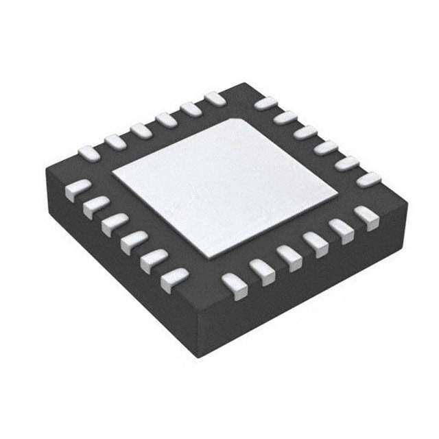
| 供应商器件封装 | 24-QFN(4x4) |
| 其它名称 | 336-2149-5 |
| 功能 | 桥,USB 至 SMBus |
| 包装 | 管件 |
| 协议 | USB |
| 参考设计库 | http://designs.digikey.com/library/4294959866/4294959865/738 |
| 商标 | Silicon Labs |
| 安装风格 | SMD/SMT |
| 封装 | Tube |
| 封装/外壳 | 24-WFQFN 裸露焊盘 |
| 封装/箱体 | QFN-24 |
| 工作温度 | -40°C ~ 85°C |
| 工作电源电压 | 3 V to 3.6 V |
| 工厂包装数量 | 91 |
| 接口 | SMBus |
| 最大工作温度 | + 85 C |
| 最小工作温度 | - 40 C |
| 标准 | USB 2.0 |
| 标准包装 | 91 |
| 电压-电源 | 1.8V,3 V ~ 3.6 V |
| 电流-电源 | 15mA |
| 系列 | CP2112 |


- 商务部:美国ITC正式对集成电路等产品启动337调查
- 曝三星4nm工艺存在良率问题 高通将骁龙8 Gen1或转产台积电
- 太阳诱电将投资9.5亿元在常州建新厂生产MLCC 预计2023年完工
- 英特尔发布欧洲新工厂建设计划 深化IDM 2.0 战略
- 台积电先进制程称霸业界 有大客户加持明年业绩稳了
- 达到5530亿美元!SIA预计今年全球半导体销售额将创下新高
- 英特尔拟将自动驾驶子公司Mobileye上市 估值或超500亿美元
- 三星加码芯片和SET,合并消费电子和移动部门,撤换高东真等 CEO
- 三星电子宣布重大人事变动 还合并消费电子和移动部门
- 海关总署:前11个月进口集成电路产品价值2.52万亿元 增长14.8%


PDF Datasheet 数据手册内容提取
Single-Chip HID USB to SMBus Master Bridge CP2112 Data Sheet The CP2112 devices are designed to quickly add USB to your applications by eliminating firmware complexity and reducing de- KEY FEATURES velopment time. • No firmware development required These highly-integrated USB-to-SMBus bridge controllers provide a simple solution for • Simple GUI-based configurator adding USB using a minimum of components and PCB space. The CP2112 includes a • Integrated USB transceiver; no external USB 2.0 full-speed function controller, USB transceiver, oscillator, and a total of 8 resistors required GPIOs in a compact 4 x 4 mm QFN-24 package. All customization and configuration • Integrated clock; no external crystal options can be selected using a simple GUI-based configurator. By eliminating the required need for complex firmware and driver development, the CP2112 devices enable quick • USB 2.0 full-speed compatible USB connectivity with minimal development effort. • Standard HID class device – no custom driver needed CP2112 is ideal for a wide range of applications, including the following: • 8 GPIOs with configurable options • USB dongles • Point-of-Sale products • Medical meters • Data loggers • Handheld controllers CP2112 Connect to VBUS or REGIN Voltage 48 MHz To External Supply VDD Regulator Oscillator SMBus SDA SMBus SCL Slave Controller GND Devices USB Interface USB Connector GPIO.0_TXT VBUS VBUS Full-Speed Peripheral GPIO.1_RXT D+ D+ 12 Mbps Function GPIO.2 D- D- Transceiver Controller GPIO.3 GPIO GND GPIO.4 Signals GPIO and GPIO.5 Suspend /RST GPIO.6 194 Byte PROM Controller VPP (Product Customization) GPIO.7_CLK I/O Power and Logic Levels /SUSPEND Logic Level Suspend Supply VIO I/O Power and Logic Levels SUSPEND Signals (1.8V to VDD) silabs.com | Smart. Connected. Energy-friendly. Rev. 1.3
CP2112Data Sheet Feature List and Ordering Information 1. Feature List and Ordering Information CP 2112 – F 03 – G M R Tape and Reel (Optional) Package Type — QFN24 Temperature Grade — –40 to +85 °C (G) Firmware Revision Hardware Revision Interface Family, HID USB-to-SMBus Bridge Silicon Labs Xpress Product Line Figure 1.1. CP2112 Part Numbering The CP2112 devices have the following features: • Single-Chip HID USB to SMBus Master Bridge • SMBus Configuration Options • Integrated USB transceiver; no external resistors or crystal • Configurable Clock Speed required • Device Address: 7-bit value that is the slave address of the • SMBus master device CP2112. The device will only ACK this address, but will not • GPIO can be configured as Input/Output and Open-Drain/ respond to any read/write requests Push-Pull • Read/Write Timeouts • 512 Byte SMBus data buffer • SCL Low Timeout • Integrated 194 Byte One-Time Programmable ROM for • Retry Counter Timeout storing customizable product information • GPIO Interface Features • On-chip power-on reset circuit • 8 GPIO pins with configurable options • On-chip voltage regulator: 3.45 V output • Usable as inputs, open-drain or push-pull outputs • USB Peripheral Function Controller • Configurable clock output for external devices • USB Specification 2.0 compliant; full-speed (12 Mbps) • 48 MHz to 94 kHz • USB Suspend states supported via SUSPEND • Toggle LED during SMBus reads and /SUSPEND pins • Toggle LED during SMBus writes • HID Interface • Supply Voltage • Standard USB class device requires no custom driver • Self-powered: 3.0 to 3.6 V • Supported on Windows, Mac, and Linux • USB bus powered: 4.0 to 5.25 V • Open access to interface specification • I/O voltage: 1.8 V to V • Windows, Mac, and Linux HID-to-SMBus Libraries DD • Ordering Part Number • APIs for quick application development • CP2112-F03-GM • Package • RoHS-compliant 24-pin QFN (4 x 4 mm) • Temperature Range: –40 to +85 °C silabs.com | Smart. Connected. Energy-friendly. Rev. 1.3 | 1
CP2112Data Sheet System Overview 2. System Overview The CP2112 is a highly-integrated HID USB-to-SMBus Bridge providing a simple solution for controlling SMBus slave devices with USB and using a minimum of components and PCB space. The CP2112 includes a USB 2.0 full-speed function controller, USB transceiver, oscillator, and a one-time programmable ROM in a compact 4 x 4 mm QFN-24 package (sometimes called “MLF” or “MLP”). The on-chip, one-time programmable ROM provides the option to customize the USB Vendor ID, Product ID, Manufacturer Product String, Product Description String, Power Descriptor, Device Release Number, and Device Serial Number as desired for OEM applica- tions. The CP2112 uses the standard USB HID device class, which is natively supported by most operating systems. A custom driver does not need to be installed for this device. Host applications communicate with the CP2112 through interface libraries provided by Silicon Labs. The interface specification for the CP2112 is also available to enable development of an API for any operating system that sup- ports HID. The CP2112 SMBus interface includes the SDA and SCL signals needed for SMBus communication and is configurable. The configura- ble options include the clock speed, read/write timeouts, retry counter timeout, SCL low timeouts, and a 7-bit device address. The CP2112 will only ACK the 7-bit device address assigned to it but will not respond to any read/write requests. External pull-up resistors are needed for the SCL and SDA signals. The device also features a total of eight GPIO signals. The GPIO signals are controlled through USB and can be configured as Input/ Output and Open-Drain/Push-Pull. Three of the GPIO signals support alternate features including a configurable clock output (48 MHz to 94 kHz) and TX and RX LED toggle. Support for I/O interface voltages down to 1.8 V is provided via a V pin. IO An evaluation kit for the CP2112 (Part Number: CP2112EK) is available. It includes a CP2112-based HID USB-to-SMBus evaluation board, Windows DLL and test application, USB cable, and full documentation. Go to www.silabs.com for the latest application notes and product support information for the CP2112. Contact a Silicon Labs sales representatives or go to http://www.silabs.com to order the CP2112 Evaluation Kit. silabs.com | Smart. Connected. Energy-friendly. Rev. 1.3 | 2
CP2112Data Sheet Electrical Specifications 3. Electrical Specifications 3.1 Electrical Characteristics All electrical parameters in all tables are specified under the conditions listed in 3.1.1 Recommended Operating Conditions, unless sta- ted otherwise. 3.1.1 Recommended Operating Conditions Table 3.1. Recommended Operating Conditions Parameter Symbol Test Condition Min Typ Max Unit Digital Supply Voltage V 3.0 — 3.6 V DD Digital Port I/O Supply Voltage V 1.8 — V V IO DD Voltage on V with respect to V V ≥ 3.3 V 5.75 — V + 3.6 V PP PP IO IO GND during a ROM programming operation Capacitor on V for ROM pro- C — 4.7 — µF PP PP gramming Supply Current 1 IDD Normal Operation; — 15 16 mA V Enabled REG Suspended; — 130 230 µA V Enabled REG Supply Current - USB Pull-up 2 IUSB — 200 228 µA Specified Operating Temperature T -40 — +85 °C A Range Note: 1.If the device is connected to the USB bus, the USB pull-up current should be added to the supply current to calculate total re- quired current. 2.The USB pull-up supply current values are calculated values based on USB specifications. silabs.com | Smart. Connected. Energy-friendly. Rev. 1.3 | 3
CP2112Data Sheet Electrical Specifications 3.1.2 SMBus, GPIO, and Suspend I/O Electrical Characteristics Table 3.2. SMBus, GPIO, and Suspend I/O Parameter Symbol Test Condition Min Typ Max Unit Output High Voltage V I = -10 µA V – 0.1 — — V OH OH IO I = -3 mA V – 0.2 — — V OH IO I = -10 mA — V – 0.4 — V OH IO Output Low Voltage V I = 10 µA — — 0.1 V OL OL I = 8.5 mA — — 0.4 V OL I = 25 mA — 0.6 — V OL Input High Voltage V 0.7 x V — — V IH IO Input Low Voltage V — — 0.6 V IL Input Leakage Current I Weak Pull-Up Off — — 1 µA LK Weak Pull-Up On, V = 0 V — 25 50 µA IO Maximum Input Voltage V Open drain, logic high (1) — — 5.8 V IN-MAX 3.1.3 Reset Electrical Characteristics Table 3.3. Reset Parameter Symbol Test Condition Min Typ Max Unit /RST Input High Voltage V 0.75 x V — — V IH-RST IO /RST Input Low Voltage V — — 0.6 V IL-RST Minimum /RST Low Time to Gen- t 15 — — μs RSTL erate a System Reset VDD Ramp Time t — — 1 ms RMP 3.1.4 Voltage Regulator Table 3.4. Voltage Regulator Parameter Symbol Test Condition Min Typ Max Unit Input Voltage Range V 3.0 — 5.25 V REGIN Output Voltage VDD Output Current = 1 to 100 mA1 3.3 3.45 3.6 V VBUS Detection Input Threshold V 2.5 — — V IH-VBUS Bias Current I — — 120 µA REG Note: 1.The maximum regulator supply current is 100 mA. This includes the supply current of the CP2112. silabs.com | Smart. Connected. Energy-friendly. Rev. 1.3 | 4
CP2112Data Sheet Electrical Specifications 3.1.5 GPIO Table 3.5. GPIO Output Specifications Parameter Symbol Test Condition Min Typ Max Unit GPIO.7 Clock Output fCLK Output x Output1 Output x Hz 0.985 1.015 TX Toggle Rate f — 10 — Hz TX RX Toggle Rate f — 10 — Hz RX Note: 1.The output frequency is configurable from 48 MHz to 94 kHz. silabs.com | Smart. Connected. Energy-friendly. Rev. 1.3 | 5
CP2112Data Sheet Electrical Specifications 3.1.6 SMBus Timing Table 3.6. SMBus Timing Performance (Master Mode) Parameter Symbol Test Condition Min Typ Max Unit Standard Mode (100 kHz Class) I2C Operating Frequency fI2C 0 — 702 kHz SMBus Operating Frequency fSMB 401 — 702 kHz Bus Free Time Between STOP and t 9.4 — — µs BUF START Conditions Hold Time After (Repeated) t 4.7 — — µs HD:STA START Condition Repeated START Condition Setup t 9.4 — — µs SU:STA Time STOP Condition Setup Time t 9.4 — — µs SU:STO Data Hold Time t 489 — — ns HD:DAT Data Setup Time t 448 — — ns SU:DAT Detect Clock Low Timeout t 25 — — ms TIMEOUT Clock Low Period t 4.7 — — µs LOW Clock High Period tHIGH 9.4 — 503 µs Fast Mode (400 kHz Class) I2C Operating Frequency fI2C 0 — 2552 kHz SMBus Operating Frequency fSMB 401 — 2552 kHz Bus Free Time Between STOP and t 2.6 — — µs BUF START Conditions Hold Time After (Repeated) t 1.3 — — µs HD:STA START Condition Repeated START Condition Setup t 2.6 — — µs SU:STA Time STOP Condition Setup Time t 2.6 — — µs SU:STO Data Hold Time t 489 — — ns HD:DAT Data Setup Time t 448 — — ns SU:DAT Detect Clock Low Timeout t 25 — — ms TIMEOUT Clock Low Period t 1.3 — — µs LOW Clock High Period tHIGH 2.6 — 503 µs Note: 1.The minimum SMBus frequency is limited by the maximum Clock High Period requirement of the SMBus specification. 2.The maximum I2C and SMBus frequencies are limited by the minimum Clock Low Period requirements of their respective specifi- cations. The maximum frequency cannot be achieved with all combinations of oscillators and dividers available, but the effective frequency must not exceed 256 kHz. 3.SMBus has a maximum requirement of 50 µs for Clock High Period. Operating frequencies lower than 40 kHz will be longer than 50 µs. I2C can support periods longer than 50 µs. silabs.com | Smart. Connected. Energy-friendly. Rev. 1.3 | 6
CP2112Data Sheet Electrical Specifications tLOW VIH SCL VIL tHD:STA tHD:DAT tHIGH tSU:DAT tSU:STA tSU:STO VIH SDA VIL tBUF P S S P Figure 3.1. SMBus Timing Diagram (Master Mode) 3.2 Absolute Maximum Ratings Stresses above those listed in 3.2 Absolute Maximum Ratings may cause permanent damage to the device. This is a stress rating only and functional operation of the devices at those or any other conditions above those indicated in the operation listings of this specifica- tion is not implied. Exposure to maximum rating conditions for extended periods may affect device reliability. For more information on the available quality and reliability data, see the Quality and Reliability Monitor Report at http://www.silabs.com/support/quality/pages/ default.aspx. Table 3.7. Absolute Maximum Ratings Parameter Symbol Test Condition Min Max Unit Ambient Temperature Under Bias T -55 125 °C BIAS Storage Temperature T -65 150 °C STG Voltage on /RST, SDA, SCL, or GPIO V VIO ≥ 2.2 V -0.3 5.8 V GPIO Pins with respect to GND VIO < 2.2 V -0.3 V + 3.6 V IO Voltage on VBUS with respect to GND V VDD ≥ 3.0 V -0.3 5.8 V BUS VDD not powered -0.3 V + 3.6 V IO Voltage on V or V with respect to V or V -0.3 4.2 V DD IO DD IO GND Maximum Total Current through V , I or I — 500 mA DD DD IO V , and GND IO Maximum Output Current sunk I — 100 mA GPIO by /RST or any I/O pin Operating Junction Temperature T -40 105 °C J Note: 1.Exposure to maximum rating conditions for extended periods may affect device reliability. silabs.com | Smart. Connected. Energy-friendly. Rev. 1.3 | 7
CP2112Data Sheet Pin Definitions 4. Pin Definitions T T X X T R _ _ 0 1 2 3 . . . . O O O O L I I I I C P P P P C S G G G G N 4 3 2 1 0 9 2 2 2 2 2 1 SDA 1 18 NC GND 2 17 /SUSPEND D+ 3 CP2112-GM 16 VPP Top View D- 4 15 GPIO.4 VIO 5 14 GPIO.5 GND (optional) VDD 6 13 GPIO.6 7 8 9 0 1 2 1 1 1 N S T C D K I U S / N L G B R N E C E V / P _ R 7 S . U O S PI G Figure 4.1. CP2112 Pin Definitions Table 4.1. Pin Definitions for CP2112 QFN24 Pin # Name Type Description 1 SDA D I/O Serial Data signal for SMBus interface. 2 GND Ground. Must be tied to ground. 3 D+ D I/O USB D+ 4 D– D I/O USB D– silabs.com | Smart. Connected. Energy-friendly. Rev. 1.3 | 8
CP2112Data Sheet Pin Definitions Pin # Name Type Description 5 VIO Power In I/O Supply Voltage Input. 6 VDD Power In Power Supply Voltage Input. Power Out Voltage Regulator Output. See Section 9. 7 REGIN Power In 5 V Regulator Input. This pin is the input to the on-chip voltage regulator. 8 VBUS D In VBUS Sense Input. This pin should be connected to the VBUS signal of a USB network. 9 RST D I/O Device Reset. Open-drain output of internal POR or VDD monitor. An external source can initiate a system reset by driving this pin low for the time specified in Table 4. 101 NC — This pin should be left unconnected or tied to VIO 111 SUSPEND D Out This pin is logic high when the CP2112 is in the USB Suspend state. 121 GPIO.7 D I/O This pin is a user-configurable input or output. CLK D Out In CLK mode, this pin outputs a clock signal whose frequency is configurable. 131 GPIO.6 D I/O This pin is a user-configurable input or output. 141 GPIO.5 D I/O This pin is a user-configurable input or output. 151 GPIO.4 D I/O This pin is a user-configurable input or output. 161 VPP Special Connect a 4.7 µF capacitor between this pin and ground to support ROM program- ming via the USB interface. 171 /SUSPEND D Out This pin is logic low when the CP2112 is in the USB Suspend state. 181, 191 NC — No connect 201 GPIO.3 D I/O This pin is a user-configurable input or output. 211 GPIO.2 D I/O This pin is a user-configurable input or output. 221 GPIO.1 D I/O This pin is a user-configurable input or output. RXT D Out In RXT mode, this pin is the Receive Toggle pin and toggles to indicate SMBus transmission. The pin is logic high when a transmission is not in progress. 231 GPIO.0 D I/O This pin is a user-configurable input or output. TXT D Out In TXT mode, this pin is the Transmit Toggle pin and toggles to indicate SMBus transmission. The pin is logic high when a transmission is not in progress. 24 SCL D I/O Serial Clock signal for SMBus interface. Center GND — Ground Note: 1.Pins can be left unconnected when not in use. silabs.com | Smart. Connected. Energy-friendly. Rev. 1.3 | 9
CP2112Data Sheet QFN24 Package Specifications 5. QFN24 Package Specifications 5.1 QFN24 Package Dimensions Figure 5.1. QFN24 Package Drawing Table 5.1. QFN24 Package Dimensions Dimension Min Typ Max A 0.70 0.75 0.80 A1 0.00 0.02 0.05 b 0.18 0.25 0.30 D 4.00 BSC. D2 2.55 2.70 2.80 e 0.50 BSC. E 4.00 BSC. E2 2.55 2.70 2.80 L 0.30 0.40 0.50 L1 0.00 — 0.15 aaa — — 0.15 silabs.com | Smart. Connected. Energy-friendly. Rev. 1.3 | 10
CP2112Data Sheet QFN24 Package Specifications Dimension Min Typ Max bbb — — 0.10 ddd — — 0.05 eee — — 0.08 Z — 0.24 — Y — 0.18 — Note: 1.All dimensions shown are in millimeters (mm) unless otherwise noted. 2.Dimensioning and Tolerancing per ANSI Y14.5M-1994. 3.This drawing conforms to JEDEC Solid State Outline MO-220, variation WGGD except for custom features D2, E2, Z, Y, and L which are toleranced per supplier designation. 4.Recommended card reflow profile is per the JEDEC/IPC J-STD-020 specification for Small Body Components. silabs.com | Smart. Connected. Energy-friendly. Rev. 1.3 | 11
CP2112Data Sheet QFN24 Package Specifications 5.2 QFN24 PCB Land Pattern Figure 5.2. QFN24 Recommended PCB Land Pattern Table 5.2. QFN24 PCB Land Pattern Dimensions Dimension Min Max C1 3.90 4.00 C2 3.90 4.00 E 0.50 BSC X1 0.20 0.30 X2 2.70 2.80 Y1 0.65 0.75 Y2 2.70 2.80 silabs.com | Smart. Connected. Energy-friendly. Rev. 1.3 | 12
CP2112Data Sheet QFN24 Package Specifications Dimension Min Max Note: General 1.All dimensions shown are in millimeters (mm) unless otherwise noted. 2.This Land Pattern Design is based on the IPC-7351 guidelines. Solder Mask Design 1.All metal pads are to be non-solder mask defined (NSMD). Clearance between the solder mask and the metal pad is to be 60 µm minimum, all the way around the pad. Stencil Design 1.A stainless steel, laser-cut and electro-polished stencil with trapezoidal walls should be used to assure good solder paste release. 2.The stencil thickness should be 0.125 mm (5 mils). 3.The ratio of stencil aperture to land pad size should be 1:1 for all perimeter pads. 4.A 2x2 array of 1.10 mm x 1.10 mm openings on 1.30 mm pitch should be used for the center ground pad. Card Assembly 1.A No-Clean, Type-3 solder paste is recommended. 2.The recommended card reflow profile is per the JEDEC/IPC J-STD-020 specification for Small Body Components. 5.3 QFN24 Package Marking SIL 2112 TTTTT YYWW+ Figure 5.3. QFN24 Package Marking The package marking consists of: • TTTTT – A trace or manufacturing code. The first letter of this code is the silicon revision. • YY – The last two digits of the assembly year. • WW – The two-digit workweek when the device was assembled. • + – Lead-free (RoHS compliance) designator. silabs.com | Smart. Connected. Energy-friendly. Rev. 1.3 | 13
CP2112Data Sheet USB Function Controller and Transceiver 6. USB Function Controller and Transceiver The Universal Serial Bus (USB) function controller in the CP2112 is a USB 2.0 compliant full-speed device with integrated transceiver and on-chip matching and pullup resistors. The USB function controller manages all data transfers between the USB and the SMBus interface as well as command requests generated by the USB host controller and commands for controlling the function of the SMBus interface and GPIO pins. The USB Suspend and Resume modes are supported for power management of both the CP2112 device and external circuitry. The CP2112 enters Suspend mode when Suspend signaling is detected on the bus. Upon entering Suspend mode, the Suspend signals are asserted. The Suspend signals are also asserted after a CP2112 reset until device configuration during USB enumeration is complete. SUSPEND is logic high when the device is in the Suspend state and logic low when the device is in normal mode. The /SUSPEND pin has the opposite logic value of the SUSPEND pin. The CP2112 exits Suspend mode when any of the following events occur: Resume signaling is detected or generated, a USB Reset signal is detected, or a device reset occurs. SUSPEND and SUSPEND are weakly pulled to VIO in a high-impedance state during a CP2112 reset. If this behavior is undesirable, a strong pulldown resistor (10 kΩ) can be used to ensure /SUSPEND remains low during reset. The eight GPIO pins will retain their state during Suspend mode. silabs.com | Smart. Connected. Energy-friendly. Rev. 1.3 | 14
CP2112Data Sheet System Management Bus (SMBus) Interface 7. System Management Bus (SMBus) Interface The SMBus I/O interface is a two-wire, bidirectional serial bus. The SMBus is compliant with the System Management Bus Specifica- tion, Version 1.1, and compatible with the I2C serial bus. Reads and writes to the interface by the system controller are byte-oriented with the SMBus interface autonomously controlling the serial transfer of the data. The CP2112 operates as an SMBus master; however, it has an SMBus slave address that is configurable. The CP2112 will only ACK this address and will not respond to any read or write requests. If the least significant bit of the address is set, the device will ignore it. 7.1 SMBus Configuration The following figure shows a typical SMBus configuration. The SMBus specification allows any recessive voltage between 3.0 V and 5.0 V; different devices on the bus may operate at different voltage levels. The bidirectional serial clock (SCL) and serial data (SDA) lines must be connected to a positive power supply voltage through a pullup resistor or similar circuit. Every device connected to the bus must have an open-drain or open-collector output for both the SCL and SDA lines so that both are pulled high (recessive state) when the bus is free. The maximum number of devices on the bus is limited only by the requirement that the rise and fall times on the bus not exceed 300 ns and 1000 ns, respectively. The SMBus provides control of SDA, SCL generation and synchronization, arbitration logic, and START/STOP control and generation. VDD = 5 V VDD = 3 V VDD = 5 V VDD = 3 V CP2112 Slave Slave (Master Device) Device 1 Device 2 SDA SCL Figure 7.1. Typical SMBus Configuration silabs.com | Smart. Connected. Energy-friendly. Rev. 1.3 | 15
CP2112Data Sheet System Management Bus (SMBus) Interface 7.2 SMBus Operation The CP2112 supports reads, writes, and addressed reads. The master device initiates all three types of data transfers and provides the clock pulses on SCL. The SMBus interface on the CP2112 operates as a master, but also has a configurable slave address associated with it that the CP2112 will only ACK upon receiving. Multiple master devices on the same bus are supported. If two or more masters attempt to initiate a data transfer simultaneously, an arbitration scheme is employed with a single master always winning the arbitration. Note that it is not necessary to specify one device as the Master in a system; any device that transmits a START and a slave address becomes the master for the duration of that transfer. A typical SMBus transaction consists of a START condition followed by an address byte (Bits7–1: 7-bit slave address; Bit0: R/W direc- tion bit), one or more bytes of data, and a STOP condition. Bytes that are received (by a master or slave) are acknowledged (ACK) with a low SDA during a high SCL (see Figures 6, 7, and 8). If the receiving device does not ACK, the transmitting device will read a NACK (not acknowledge), which is a high SDA during a high SCL. The direction bit (R/W) occupies the least-significant bit position of the address byte. The direction bit is set to logic 1 to indicate a "READ" operation and cleared to logic 0 to indicate a "WRITE" operation. All transactions are initiated by a master, with one or more addressed slave devices as the target. The master generates the START condition and then transmits the slave address and direction bit. If the transaction is a WRITE operation from the master to the slave, the master transmits the data one byte at a time waiting for an ACK from the slave at the end of each byte. For READ operations, the slave transmits the data waiting for an ACK from the master at the end of each byte. At the end of the data transfer, the master generates a STOP condition to terminate the transaction and free the bus. The first figure illustrates a typical CP2112 read transaction, and the second figure illustrates a typical CP2112 write transaction. SCL SDA SLA6 SLA5-0 Read (1) D7 D6-0 START Slave Address + Read ACK Data Byte NACK STOP Figure 7.2. Typical CP2112 Read SCL SDA SLA6 SLA5-0 Write (0) D7 D6-0 START Slave Address + Write ACK Data Byte ACK STOP Figure 7.3. Typical CP2112 Write The CP2112 performs addressed reads using a repeated start. Addressed Reads are implemented by issuing a START condition fol- lowed by a slave address write and logical address. Next the CP2112 issues a repeated START followed by a slave address read. After this sequence, the CP2112 reads bytes from the slave device. The CP2112 supports addressed reads on slave devices with up to a 16 byte logical address field. The following figure illustrates a typical addressed read transaction (with a one byte logical address field). SCL SDA SLA6-0 Write (0) ADDR7-0 SLA6-0 Read (1) DATA7-0 Logical Repeated START Slave Address + Write ACK ACK Slave Address + Read ACK Data Byte NACK STOP Address START Figure 7.4. Typical CP2112 Addressed Read silabs.com | Smart. Connected. Energy-friendly. Rev. 1.3 | 16
CP2112Data Sheet System Management Bus (SMBus) Interface 7.3 CP2112 Configuration Options The CP2112 has the following SMBus configuration options, which are all configured through USB: clock speed, device address, auto send read, read timeout, write timeout, SCL low timeout, and retry time. • The SMBus clock speed is configurable with a recommended operating range of 10 kHz to 400 kHz. • The device address is a configurable 7-bit address, which is the slave address of the CP2112. Although the CP2112 is a master device, the CP2112 will ACK this address but will not respond to any read or write requests. If the least significant bit is set, the CP2112 will ignore it. • If auto read send is set to 0x01, the CP2112 will return the results of a read automatically. If this is set to 0x00, the device will wait for a "data read response" request to respond to data. • The read and write timeouts are the time limit before the device will automatically cancel a transfer that has been initiated and can range from 0 to 1000 ms. If set to 0 ms, this indicates that there is no timeout. • The SCL low timeout is either enabled or disabled. If the SCL line is held low by a slave device on the bus, no further communication is possible. Furthermore, the master cannot force the SCL line high to correct the error condition. To solve this problem, the SMBus protocol specifies that devices participating in a transfer must detect any clock cycle held low longer than 25 ms as a "timeout" con- dition. Devices that have detected the timeout condition must reset the communication no later than 10 ms after detecting the time- out condition. • The retry time is the number of times the device will attempt a transfer before terminating the transfer. This can be set from 0 to 1000. If set to 0, there is no retry limit. These configuration options cannot be changed while a transfer is in progress. silabs.com | Smart. Connected. Energy-friendly. Rev. 1.3 | 17
CP2112Data Sheet GPIO Pins 8. GPIO Pins The CP2112 supports 8 user-configurable GPIO pins. Each of these GPIO pins are usable as inputs, open-drain outputs, or push-pull outputs. Three of these GPIO pins also have alternate functions which are listed in the following table. Table 8.1. GPIO Pin Alternate Functions GPIO Pin Alternate Function GPIO.0 TX Toggle GPIO.1 RX Toggle GPIO.7 CLK Output By default, all of the GPIO pins are configured as a GPIO input. The pins must be configured each time the device is reset. For exam- ple, if a device is unplugged and then plugged into a PC, the GPIO pins would be configured as inputs and would need to be reconfig- ured as needed. The difference between an open-drain output and a push-pull output is when the GPIO output is driven to logic high. A logic high, open- drain output pulls the pin to the VIO rail through an internal, pull-up resistor. A logic high, push-pull output directly connects the pin to the VIO voltage. Open-drain outputs are typically used when interfacing to logic at a higher voltage than the VIO pin. These pins can be safely pulled to the higher, external voltage through an external pull-up resistor. The maximum external pull-up voltage is 5 V. The speed of reading and writing the GPIO pins is subject to the timing of the USB bus. GPIO pins configured as inputs or outputs are not recommended for real-time signaling. 8.1 GPIO.0-1—Transmit and Receive Toggle GPIO.0 and GPIO.1 are configurable as Transmit Toggle and Receive Toggle pins. These pins are logic high when a device is not transmitting or receiving data, and they toggle at a fixed rate as specified in Table 3.5 GPIO Output Specifications on page 5 when data transfer is in progress. Typically, these pins are connected to two LEDs to indicate data transfer. VIO CP2112 GPIO.0 – TX Toggle GPIO.1 – RX Toggle Figure 8.1. Transmit and Receive Toggle Typical Connection Diagram 8.2 GPIO.7—Clock Output (CLK) GPIO.7 is configurable to output a configurable CMOS clock output. The clock output appears at the pin at the same time the device completes enumeration and exits USB Suspend mode. The clock output is removed from the pin when the device enters USB Suspend mode. The output frequency is configurable through the use of a divider and the accuracy is specified in Table 6. When the divider is set to 0, the output frequency is 48 MHz. For divider values between 1 and 255, the output frequency is determined by the formula: 48MHz GPIO.7ClockFrequency= 2×ClockDivider silabs.com | Smart. Connected. Energy-friendly. Rev. 1.3 | 18
CP2112Data Sheet One-Time Programmable ROM 9. One-Time Programmable ROM The CP2112 includes an internal, one-time programmable ROM that may be used to customize the USB vendor ID (VID), product ID (PID), manufacturer string, product description string, power descriptor, device release number, and device serial number as desired for OEM applications. If the programmable ROM has not been customized, the default configuration data shown in the table below is used. Table 9.1. Default USB Configuration Data Name Description Default Value Vendor ID (VID) The Vendor ID is a four digit hexadecimal number that is 10C4h unique to a particular vendor. 10C4h, for example, is the Silicon Labs Vendor ID. Product ID (PID) The Product ID is a four digit hexadecimal number that EA90h identifies the vendor's device. EA90h, for example, is the default Product ID for Silicon Labs' CP2112 HID USB-to- SMBus Bridge devices. Power Descriptor (Attrib- This setting determines whether the device is Bus-Pow- 80h (Bus-Powered) utes) ered, i.e. it is powered by the host, or Self-Powered, i.e. it is powered from a supply on the device. Power Descriptor (Max This describes the maximum amount of power that the de- 32h (100 mA) Power) vice will draw from the host in mA multiplied by 2. For ex- ample, 32h equates to 100 mA. Release Number The Release Version is a binary-coded-decimal value that 0100h (Release Version 01.00) is assigned by the device manufacturer. Manufacturer String This string is customizable and can be a maximum of 30 "Silicon Laboratories" (30 ASCII characters ASCII characters. maximum) Product Description String The Product String is an optional string that describes the "CP2112 HID USB-to-SMBus Bridge" (30 product. It is limited to 30 ASCII characters. ASCII characters maximum) Serial String The Serial String is an optional string that is used by the Unique 8-character ASCII string (30 ASCII host to distinguish between multiple devices with the same characters maximum) VID and PID combination. It is limited to 30 ASCII charac- ters. While customization of the USB configuration data is optional, customizing the VID/PID combination is strongly recommended. A unique VID/PID will prevent the device from being recognized by any other manufacturer’s software application. A vendor ID can be obtained from www.usb.org, or Silicon Labs can provide a free PID for the OEM product that can be used with the Silicon Labs VID. Customizing the serial string for each individual device is also recommended if the OEM application is one in which it is possible for multiple CP2112-based devices to be connected to the same PC. AN495: CP2112 Interface Specification includes more information about the programmable values and their valid options. Note that certain items in the PROM are programmed as a group, and programming one of these items in a group prevents further programming of any of the other items in the group. The configuration data ROM is programmable by Silicon Labs prior to shipment with the desired configuration information. It can also be programmed in-system over the USB interface by adding a capacitor to the PCB. If configuration ROM is to be programmed in- system, a 4.7 µF capacitor must be added between the VPP pin and ground. No other circuitry should be connected to VPP during a programming operation, and VIO must remain at 3.3 V or higher to successfully write to the configuration ROM. silabs.com | Smart. Connected. Energy-friendly. Rev. 1.3 | 19
CP2112Data Sheet Voltage Regulator 10. Voltage Regulator The CP2112 includes an on-chip 5.0 to 3.45 V voltage regulator. This allows the CP2112 to be configured as either a USB bus-pow- ered device or a USB self-powered device. A typical connection diagram of the device in a bus-powered application using the regulator is shown in Figure 10.1 Typical Bus-Powered Connection Diagram on page 20. When enabled, the voltage regulator output appears on the V pin and can be used to power external devices. See 3.1.4 Voltage Regulator for the voltage regulator electrical characteris- DD tics. If the regulator is used to provide VDD in a self-powered application, use the same connections from Figure 10.1 Typical Bus-Powered Connection Diagram on page 20, but connect REGIN to an onboard 5 V supply, and disconnect it from the VBUS pin. In addition, if REGIN may be unpowered while VBUS is 5 V, a resistor divider shown in Note 5 of Figure 10.2 Typical Self-Powered Connection Dia- gram (Regulator Bypass) on page 21 is required to meet the absolute maximum voltage on VBUS specification in 3.2 Absolute Maxi- mum Ratings. Note 2 VIO 4.7 k CP2112 Note 3 VIO /RST /SUSPEND Suspend SUSPEND Signals 3.3 V Power VDD VPP Note 4 1-5 µF 0.1 µF 4.7 µF REGIN To SDA SMBus SCL Slave 1 µF Devices GPIO.0_TXT GND GPIO.1_RXT USB GPIO.2 Connector GPIO.3 VBUS VBUS GPIO Signals GPIO.4 D+ D+ D- D- GPIO.5 GND GPIO.6 GPIO.7_CLK Note 1 Note 1 : Avalanche transient voltage suppression diodes compatible with Full-speed USB should be added at the connector for ESD protection. Use Littelfuse p/n SP0503BAHT or equivalent. Note 2 : An external pull-up is not required, but can be added for noise immunity. Note 3 : VIO can be connected directly to VDD or to a supply as low as 1.8 V to set the I/O interface voltage. Note 4 : If programming the configuration ROM via USB, add a 4.7 µF capacitor between VPP and ground. During a programming operation, do not connect the VPP pin to other circuitry, and ensure that VIO is at least 3.3 V. Figure 10.1. Typical Bus-Powered Connection Diagram silabs.com | Smart. Connected. Energy-friendly. Rev. 1.3 | 20
CP2112Data Sheet Voltage Regulator Alternatively, if 3.0 to 3.6 V power is supplied to the VDD pin, the CP2112 can function as a USB self-powered device with the voltage regulator bypassed. For this configuration, tie the REGIN input to VDD to bypass the voltage regulator. A typical connection diagram showing the device in a self-powered application with the regulator bypassed is shown in the following figure. The USB max power and power attributes descriptor must match the device power usage and configuration. See the Xpress Configura- tor utility within Simplicity Studio (www.silabs.com/simplicity) for information on how to customize USB descriptors for the CP2112. Note 2 VIO 4.7 k CP2112 Note 3 VIO /RST /SUSPEND Suspend VDD SUSPEND Signals 3.3 V REGIN Power VPP Note 4 4.7 µF 1-5 µF 0.1 µF To SDA SMBus SCL Slave Devices GPIO.0_TXT GND GPIO.1_RXT GPIO.2 Note 5 GPIO.3 (Optional) 24 k GPIO Signals USB VBUS GPIO.4 Connector 47 k GPIO.5 VBUS GPIO.6 D+ D+ GPIO.7_CLK D- D- GND Note 1 Note 1 : Avalanche transient voltage suppression diodes compatible with Full-speed USB should be added at the connector for ESD protection. Use Littelfuse p/n SP0503BAHT or equivalent. Note 2 : An external pull-up is not required, but can be added for noise immunity. Note 3 : VIO can be connected directly to VDD or to a supply as low as 1.8 V to set the I/O interface voltage. Note 4 : If programming the configuration ROM via USB, add a 4.7 µF capacitor between VPP and ground. During a programming operation, do not connect the VPP pin to other circuitry, and ensure that VIO is at least 3.3 V. Note 5 : For self-powered systems where VDD and VIO may be unpowered when VBUS is connected to 5 V, a resistor divider (or functionally-equivalent circuit) on VBUS is required to meet the absolute maximum voltage on VBUS specification in the Electrical Characteristics section. Figure 10.2. Typical Self-Powered Connection Diagram (Regulator Bypass) silabs.com | Smart. Connected. Energy-friendly. Rev. 1.3 | 21
CP2112Data Sheet Relevant Application Notes and Software 11. Relevant Application Notes and Software The following Application Notes are applicable to the CP2112 devices. The latest versions of these application notes and their accom- panying software are available at www.silabs.com/interface-appnotes or within Simplicity Studio in the [Application Notes] area. • AN721: CP210x Device Customization Guide — This application note guides developers through the configuration process of devi- ces using Simplicity Studio [Xpress Configurator]. • AN495: CP2112 Interface Specification — This document describes how to interface to the CP2112 using the low-level, HID Inter- face. • AN496: CP2112 HID USB-to-SMBus API Specification — This document describes how to interface to the CP2112 using the inter- face library, available for various operating systems. The CP2112 Software Development Kit can be downloaded from www.silabs.com/interface-software. See the Xpress Configurator utili- ty in Simplicity Studio (www.silabs.com/simplicity) for information on how to customize USB descriptors for the CP2112. The CP2112 is a USB Human Interface Device (HID), and, since most operating systems include native drivers, custom drivers do not need to be installed. Because the CP2112 does not fit a standard HID device type, such as a keyboard or mouse, any CP2112 PC application needs to use the CP2112's HID specification to communicate with the device. The low-level HID specification for the CP2112 is provided in AN495: CP2112 Interface Specification. This document describes all of the basic functions for opening, reading from, writing to, and closing the device, as well as the ROM programming functions. An interface library is available for various operating systems that encapsulates the CP2112 HID interface and also adds higher level features, such as read/write timeouts is provided by Silicon Labs. This library is the recommended interface for the CP2112. The inter- face library is documented in AN496: CP2112 HID USB-to-SMBus API Specification. silabs.com | Smart. Connected. Energy-friendly. Rev. 1.3 | 22
CP2112Data Sheet Revision History 12. Revision History 12.1 Revision 1.3 February 1st, 2017 Updated orderable part number to CP2112-F03-GM. Updated document formatting. Removed specific operating system versions supported. Added 3.1.6 SMBus Timing. Added Operating Junction Temperature to Table 3.7 Absolute Maximum Ratings on page 7. Swapped the pin number and name columns in Table 4.1 Pin Definitions for CP2112 QFN24 on page 8 and reordered the rows based on pin number. Also added the GND center pad to the table. Added 5.3 QFN24 Package Marking. Added the Description column to Table 9.1 Default USB Configuration Data on page 19. Updated all references from VDD to VIO when discussing minimum voltage requirements when programming the One-Time Program- mable ROM. Updated Figure 10.1 Typical Bus-Powered Connection Diagram on page 20 and Figure 10.2 Typical Self-Powered Connection Diagram (Regulator Bypass) on page 21 to remove an extra, erroneous GPIO. Updated all references of CP2112_SetIDs to Xpress Configurator in Simplicity Studio. Combined the CP2112 Interface Specification and Windows Interface DLL and 11. Relevant Application Notes and Software into one section. Removed the Device Specific Behavior section and moved this information to the device errata. 12.2 Revision 1.2 November 2013 Added a row for VBUS in 3.2 Absolute Maximum Ratings. Added VDD Ramp Time for Power On specification to 3.1.3 Reset Electrical Characteristics. Added VPP Voltage and Capacitor specifications to 3.1.1 Recommended Operating Conditions. Removed AN144 references. Added references to the CP2112_SetIDs software and CP2112 SDK. Updated 10. Voltage Regulator to add absolute maximum voltage on VBUS requirements in self-powered systems. 12.3 Revision 1.1 July 2011 Updated ordering part number. Updated 7.2 SMBus Operation to describe SMBus transactions supported by CP2112. Updated Figure 7.2 Typical CP2112 Read on page 16 and added Figure 7.3 Typical CP2112 Write on page 16 and Figure 7.4 Typical CP2112 Addressed Read on page 16. Added Device Specific Behavior chapter, which documents the differences between revisions F01 and F02. 12.4 Revision 1.0 October 2010 Removed preliminary language. silabs.com | Smart. Connected. Energy-friendly. Rev. 1.3 | 23
CP2112Data Sheet Revision History 12.5 Revision 0.5 Updated 3.1.2 SMBus, GPIO, and Suspend I/O Electrical Characteristics. Updated 3.1.3 Reset Electrical Characteristics. Updated 3.1.4 Voltage Regulator. Updated Table 9.1 Default USB Configuration Data on page 19. 12.6 Revision 0.1 May 2010 Initial release. silabs.com | Smart. Connected. Energy-friendly. Rev. 1.3 | 24
Table of Contents 1. Feature List and Ordering Information . . . . . . . . . . . . . . . . . . . . . . 1 2. System Overview. . . . . . . . . . . . . . . . . . . . . . . . . . . . . . 2 3. Electrical Specifications . . . . . . . . . . . . . . . . . . . . . . . . . . . 3 3.1 Electrical Characteristics . . . . . . . . . . . . . . . . . . . . . . . . . . 3 3.1.1 Recommended Operating Conditions . . . . . . . . . . . . . . . . . . . . . 3 3.1.2 SMBus, GPIO, and Suspend I/O Electrical Characteristics . . . . . . . . . . . . . . 4 3.1.3 Reset Electrical Characteristics . . . . . . . . . . . . . . . . . . . . . . . 4 3.1.4 Voltage Regulator . . . . . . . . . . . . . . . . . . . . . . . . . . . . 4 3.1.5 GPIO . . . . . . . . . . . . . . . . . . . . . . . . . . . . . . . . 5 3.1.6 SMBus Timing . . . . . . . . . . . . . . . . . . . . . . . . . . . . . 6 3.2 Absolute Maximum Ratings . . . . . . . . . . . . . . . . . . . . . . . . . 7 4. Pin Definitions. . . . . . . . . . . . . . . . . . . . . . . . . . . . . . . 8 5. QFN24 Package Specifications. . . . . . . . . . . . . . . . . . . . . . . . 10 5.1 QFN24 Package Dimensions. . . . . . . . . . . . . . . . . . . . . . . . .10 5.2 QFN24 PCB Land Pattern. . . . . . . . . . . . . . . . . . . . . . . . . .12 5.3 QFN24 Package Marking . . . . . . . . . . . . . . . . . . . . . . . . . .13 6. USB Function Controller and Transceiver . . . . . . . . . . . . . . . . . . . 14 7. System Management Bus (SMBus) Interface . . . . . . . . . . . . . . . . . . 15 7.1 SMBus Configuration . . . . . . . . . . . . . . . . . . . . . . . . . . .15 7.2 SMBus Operation . . . . . . . . . . . . . . . . . . . . . . . . . . . .16 7.3 CP2112 Configuration Options . . . . . . . . . . . . . . . . . . . . . . . .17 8. GPIO Pins . . . . . . . . . . . . . . . . . . . . . . . . . . . . . . . 18 8.1 GPIO.0-1—Transmit and Receive Toggle . . . . . . . . . . . . . . . . . . . .18 8.2 GPIO.7—Clock Output (CLK) . . . . . . . . . . . . . . . . . . . . . . . .18 9. One-Time Programmable ROM. . . . . . . . . . . . . . . . . . . . . . . . 19 10. Voltage Regulator . . . . . . . . . . . . . . . . . . . . . . . . . . . . 20 11. Relevant Application Notes and Software . . . . . . . . . . . . . . . . . . . 22 12. Revision History. . . . . . . . . . . . . . . . . . . . . . . . . . . . . 23 12.1 Revision 1.3 . . . . . . . . . . . . . . . . . . . . . . . . . . . . . .23 12.2 Revision 1.2 . . . . . . . . . . . . . . . . . . . . . . . . . . . . . .23 12.3 Revision 1.1 . . . . . . . . . . . . . . . . . . . . . . . . . . . . . .23 12.4 Revision 1.0 . . . . . . . . . . . . . . . . . . . . . . . . . . . . . .23 12.5 Revision 0.5 . . . . . . . . . . . . . . . . . . . . . . . . . . . . . .24 12.6 Revision 0.1 . . . . . . . . . . . . . . . . . . . . . . . . . . . . . .24 Table of Contents. . . . . . . . . . . . . . . . . . . . . . . . . . . . . . 25 Table of Contents 25
Simplicity Studio One-click access to MCU and wireless tools, documentation, software, source code libraries & more. Available for Windows, Mac and Linux! IoT Portfolio SW/HW Quality Support and Community www.silabs.com/IoT www.silabs.com/simplicity www.silabs.com/quality community.silabs.com Disclaimer Silicon Labs intends to provide customers with the latest, accurate, and in-depth documentation of all peripherals and modules available for system and software implementers using or intending to use the Silicon Labs products. Characterization data, available modules and peripherals, memory sizes and memory addresses refer to each specific device, and "Typical" parameters provided can and do vary in different applications. Application examples described herein are for illustrative purposes only. Silicon Labs reserves the right to make changes without further notice and limitation to product information, specifications, and descriptions herein, and does not give warranties as to the accuracy or completeness of the included information. Silicon Labs shall have no liability for the consequences of use of the information supplied herein. This document does not imply or express copyright licenses granted hereunder to design or fabricate any integrated circuits. The products are not designed or authorized to be used within any Life Support System without the specific written consent of Silicon Labs. A "Life Support System" is any product or system intended to support or sustain life and/or health, which, if it fails, can be reasonably expected to result in significant personal injury or death. Silicon Labs products are not designed or authorized for military applications. Silicon Labs products shall under no circumstances be used in weapons of mass destruction including (but not limited to) nuclear, biological or chemical weapons, or missiles capable of delivering such weapons. Trademark Information Silicon Laboratories Inc.® , Silicon Laboratories®, Silicon Labs®, SiLabs® and the Silicon Labs logo®, Bluegiga®, Bluegiga Logo®, Clockbuilder®, CMEMS®, DSPLL®, EFM®, EFM32®, EFR, Ember®, Energy Micro, Energy Micro logo and combinations thereof, "the world’s most energy friendly microcontrollers", Ember®, EZLink®, EZRadio®, EZRadioPRO®, Gecko®, ISOmodem®, Precision32®, ProSLIC®, Simplicity Studio®, SiPHY®, Telegesis, the Telegesis Logo®, USBXpress® and others are trademarks or registered trademarks of Silicon Labs. ARM, CORTEX, Cortex-M3 and THUMB are trademarks or registered trademarks of ARM Holdings. Keil is a registered trademark of ARM Limited. All other products or brand names mentioned herein are trademarks of their respective holders. Silicon Laboratories Inc. 400 West Cesar Chavez Austin, TX 78701 USA http://www.silabs.com
Mouser Electronics Authorized Distributor Click to View Pricing, Inventory, Delivery & Lifecycle Information: S ilicon Laboratories: CP2112-F01-GM CP2112-F02-GM CP2112-F01-GMR CP2112-F02-GMR CP2112-F03-GM CP2112-F03-GMR