 Datasheet下载
- 型号: CP2114-B01-GM
- 制造商: Silicon Laboratories
- 库位|库存: xxxx|xxxx
- 要求:
| 数量阶梯 | 香港交货 | 国内含税 |
| +xxxx | $xxxx | ¥xxxx |
查看当月历史价格
查看今年历史价格
CP2114-B01-GM产品简介:
ICGOO电子元器件商城为您提供CP2114-B01-GM由Silicon Laboratories设计生产,在icgoo商城现货销售,并且可以通过原厂、代理商等渠道进行代购。 CP2114-B01-GM价格参考。Silicon LaboratoriesCP2114-B01-GM封装/规格:接口 - 控制器, USB 桥,USB 至 I²S USB 2.0 I²S 接口 32-QFN(5x5)。您可以下载CP2114-B01-GM参考资料、Datasheet数据手册功能说明书,资料中有CP2114-B01-GM 详细功能的应用电路图电压和使用方法及教程。
Silicon Labs 的 CP2114-B01-GM 是一款高性能的 USB 至 UART/HCI 桥接控制器,属于接口-控制器类芯片。该器件广泛应用于需要将 USB 接口转换为串行通信接口(如 UART)或蓝牙主机控制器接口(HCI)的场景。

典型应用场景包括:

1. 蓝牙模块开发:CP2114 常用于蓝牙 4.2 和 BLE(低功耗蓝牙)设备的开发中,作为主机与蓝牙模块之间的桥接芯片,实现 PC 或嵌入式系统通过 USB 接口与蓝牙设备的通信。

2. 工业控制与嵌入式系统:在工业自动化和嵌入式系统中,该芯片可用于连接主控单元与各种串口设备,如传感器、PLC、仪表等,提供稳定可靠的 USB 转串口通信功能。

3. 调试与测试设备:因其支持多种通信协议,CP2114 可用于开发调试工具,帮助工程师进行硬件调试、固件更新及协议分析。

4. 消费类电子产品:如智能家电、穿戴设备等,用于实现设备与 PC 或移动设备之间的数据传输与控制。

该芯片集成度高,内置 USB 收发器、振荡器和 SRAM,支持多种电源管理模式,具有低功耗、易集成的特点,适合对空间和功耗有要求的应用场景。
| 参数 | 数值 |
| 产品目录 | 集成电路 (IC)半导体 |
| 描述 | IC USB-TO-I2S AUDIO BRIDGE 32QFN输入/输出控制器接口集成电路 USB to I2S Audio bridge |
| 产品分类 | 线性 - 音频处理集成电路 - IC |
| 品牌 | Silicon Laboratories IncSilicon Labs |
| 产品手册 | |
| 产品图片 |
|
| rohs | 符合RoHS无铅 / 符合限制有害物质指令(RoHS)规范要求 |
| 产品系列 | 接口 IC,输入/输出控制器接口集成电路,Silicon Labs CP2114-B01-GM- |
| 数据手册 | |
| 产品型号 | CP2114-B01-GMCP2114-B01-GM |
| USB修订版 | |
| 产品 | I/O Controller |
| 产品培训模块 | http://www.digikey.cn/PTM/IndividualPTM.page?site=cn&lang=zhs&ptm=26153 |
| 产品种类 | 输入/输出控制器接口集成电路 |
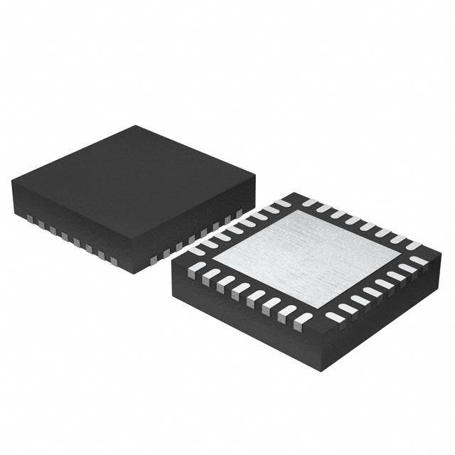
| 供应商器件封装 | 32-QFN(5x5) |
| 其它名称 | 336-2287-5 |
| 包装 | 管件 |
| 参考设计库 | http://designs.digikey.com/library/4294959866/4294959865/943http://designs.digikey.com/library/4294959866/4294959865/999 |
| 商标 | Silicon Labs |
| 安装类型 | 表面贴装 |
| 安装风格 | SMD/SMT |
| 封装 | Tube |
| 封装/外壳 | 32-VFQFN 裸露焊盘 |
| 封装/箱体 | QFN-32 |
| 工作温度 | - 40 C to + 85 C |
| 工作温度范围 | - 40 C to + 85 C |
| 工作电源电压 | 3 V to 3.6 V |
| 工厂包装数量 | 73 |
| 应用 | USB 至 I²S |
| 接口类型 | I2C, I2S, UART |
| 最大工作温度 | + 85 C |
| 最小工作温度 | - 40 C |
| 标准包装 | 73 |
| 类型 | 数字音频桥Digital Audio Bridge |
| 系列 | CP2114 |
| 输入/输出端数量 | 12 |
| 配用 | /product-detail/zh/CP2114EK/336-2291-ND/3474372/product-detail/zh/CP2114-PCM1774EK/336-2290-ND/3474371/product-detail/zh/CP2114-WM8523EK/336-2289-ND/3474370/product-detail/zh/CP2114-CS42L55EK/336-2288-ND/3474369 |


- 商务部:美国ITC正式对集成电路等产品启动337调查
- 曝三星4nm工艺存在良率问题 高通将骁龙8 Gen1或转产台积电
- 太阳诱电将投资9.5亿元在常州建新厂生产MLCC 预计2023年完工
- 英特尔发布欧洲新工厂建设计划 深化IDM 2.0 战略
- 台积电先进制程称霸业界 有大客户加持明年业绩稳了
- 达到5530亿美元!SIA预计今年全球半导体销售额将创下新高
- 英特尔拟将自动驾驶子公司Mobileye上市 估值或超500亿美元
- 三星加码芯片和SET,合并消费电子和移动部门,撤换高东真等 CEO
- 三星电子宣布重大人事变动 还合并消费电子和移动部门
- 海关总署:前11个月进口集成电路产品价值2.52万亿元 增长14.8%


PDF Datasheet 数据手册内容提取
USBXpress™ USB Audio to I2S Digital Audio Bridge Family CP2114 Data Sheet The CP2114 devices, part of the USBXpress family, are designed KEY FEATURES to enable rapid development of USB-based audio applications. • Single chip USB Audio to I2S Digital Audio The CP2114 simplifies the process of transferring audio data from USB to I2S without Bridge any code development, speeding time to market for USB audio accessories such as • Supports USB HID Consumer Controls for USB speakers, USB headphones and USB music boxes, as well as VoIP systems. The Volume and Mute Synchronization CP2114 includes a USB 2.0 full-speed function controller, USB transceiver, oscillator, • Integrated USB transceiver; no external I2S (audio) interface, I2C (control) interface and UART interface in a compact 5 x 5 mm resistors required QFN-32 package ideal for space-constrained portable audio applications. • Integrated clock; no external crystal required CP2114 is ideal for a wide range of USB Audio applications, including the following: • On-chip voltage regulator: 3.45 V output • USB speakers • USB headphones/headsets • Self-powered or Bus-powered • MP3 accessories • Point of sale terminals • No firmware development required • Navigation systems • Music boxes CP2114 Connect to VBUS or REGIN Voltage Internal Baud Rate UART GPIO.10_TX External Supply VDD Regulator Oscillator Generator Controller GPIO.11_RX UART GND USB Interface GPIO.0_RMUTE USB GPIO.1_PMUTE Connector USB UART FIFOs GPIO.2_VOL+ Volume/Mute Controls VBUS VBUS Full-Speed 256 B RX GPIO.3_VOL- D+ D+ Transceiver 256 B TX GPIO.4_RMUTELED D- D- GPIO and GPIO.5_TXT_CFGSEL0 GND Peripheral Suspend GPIO.6_RXT_CFGSEL1 Controller Controller Config GPIO.7_RTS_CFGSEL2 Selection Audio FIFOs RST GPIO.8_CTS_CFGSEL3 352 Byte PROM Play: 256 samples GPIO.9_CLKOUT Clock Output (optional) VPP (USB Customization) Rec: 256 samples SUSPEND Suspend Signals SUSPEND Logic Level Supply VIO I/O Power and Audio Controller SDA Logic Levels (1.8V to VDD) SCL CS42L55 Configuration MCLK Support for 32 SCK I2S and I2C Signals to CODEC PCM1774 Configuration User-Programmed LRCK Audio Configurations SDIN WM8523 Configuration SDOUT EXTCLK External Clock Input silabs.com | Smart. Connected. Energy-friendly. Rev. 1.2
CP2114 Data Sheet Feature List and Ordering Information 1. Feature List and Ordering Information CP 2114 – B 02 – G M R Tape and Reel (Optional) Package Type — QFN32 Temperature Grade — –40 to +85 °C (G) Firmware Revision Hardware Revision USBXpress Family, USB Audio to I2S Digital Audio Bridge Silicon Labs Xpress Product Line Figure 1.1. CP2114 Part Numbering The CP2114 devices have the following features: • Single-Chip USB Audio to I2S Digital Audio Bridge • USB Peripheral Function Controller • USB HID to I2C to communicate with codecs • USB Specification 2.0 compliant; full-speed (12 Mbps) • Supports I2C communication with other slave devices in • USB Suspend states supported via SUSPEND pins the system (B02 only) • USB HID to UART Auxiliary Communication Interface • Supports I2S and left-justified audio interface formats • APIs for quick application development • Supports USB HID Consumer Controls for Volume and • HID devices natively supported by Windows/Mac/Linux Mute Controls • 12 Configurable GPIO Pins with Alternate Functions • Integrated USB transceiver • Usable as inputs, open-drain or push-pull outputs • Integrated clock; no external crystal required • UART signals, audio playback controls, codec select pins • Integrated One-Time Programmable ROM for product cus- • Configurable clock output tomization • Toggle LEDs upon UART transmission or reception • On-chip voltage regulator • Supply Voltage • Supports a Wide Range of codecs • Self-powered: 3.0 to 3.6 V • Preloaded configurations for three popular codec DAC de- • USB bus powered: 4.0 to 5.25 V vices • I/O voltage: 1.8 V to V • Internal programmable memory supports additional codec DD configurations • Package • USB Audio Class v1.0 support • RoHS-compliant 32-pin QFN (5 x 5 mm) • Natively supported (no custom driver required) on Win- • Ordering Part Number dows/Mac/Linux/iOS • CP2114-B02-GM • Supports 16-bit Play/Record at 48 kHz sample rate • CP2114-B01-GM (not recommended for new designs) • Also supports 24-bit Play or Record (CP2114-B02 only) • Temperature Range: –40 to +85 °C • Supports Asynchronous or Synchronous Modes Note: 1.For brevity, the term 'codec' is used to refer to the external audio device, which may be a codec, DAC, or ADC. The terms 'DAC' and 'ADC' are used when the context is applicable to only those devices. 2.The CP2114 may not operate correctly when connected to a USB hub. The most common problem in this configuration is audio packet loss. silabs.com | Smart. Connected. Energy-friendly. Rev. 1.2 | 1
CP2114 Data Sheet Electrical Specifications 2. Electrical Specifications 2.1 Electrical Characteristics All electrical parameters in all tables are specified under the conditions listed in 2.1.1 Recommended Operating Conditions, unless sta- ted otherwise. 2.1.1 Recommended Operating Conditions Table 2.1. Recommended Operating Conditions Parameter Symbol Test Condition Min Typ Max Unit Digital Supply Voltage (V ) V 3.0 — 3.6 V DD DD Digital Port I/O Supply Voltage V 1.8 — V V IO DD (V ) IO Digital Supply Current (USB Active I Bus Powered Mode — 18 28 mA DD Mode)1 Self Powered Mode with Regulator enabled Self Powered Mode with Regulator disabled Digital Supply Current (USB Sus- I Bus Powered Mode — 750 940 µA DD pend Mode)1 Self Powered Mode with Regulator enabled Self Powered Mode with Regulator — 0.99 1.2 mA disabled Supply Current - USB Pull-up2 IPU — 200 228 µA Operating Ambient Temperature T -40 — 85 °C A Note: 1.If the device is connected to the USB bus, the USB Pull-up Current should be added to the supply current for total supply current. 2.The USB Pull-up supply current values are calculated values based on USB specifications. silabs.com | Smart. Connected. Energy-friendly. Rev. 1.2 | 2
CP2114 Data Sheet Electrical Specifications 2.1.2 I2S, I2C, UART and Suspend I/O Table 2.2. I2S, I2C, UART and GPIO DC Electrical Characteristics Parameter Symbol Test Condition Min Typ Max Unit Output High Voltage V I = -10 µA V - 0.1 — — V OH OH IO I = -3 mA V - 0.2 — — V OH IO I = -10 mA — V - 0.4 — V OH IO Output Low Voltage V I = 10 µA — — 0.1 V OL OL I = 8.5 mA — — 0.4 V OL I = 25 mA — 0.6 — V OL Input High Voltage V V x 0.7 — — V IH IO Input Low Voltage V — — 0.6 V IL Input Leakage Current I Weak Pull-Up Off — — 1 μA LK Weak Pull-Up On, V = 0 V — 25 50 μA IO Maximum Input Voltage V Open drain, logic high (1) — — 5.8 V IN_MAX 2.1.3 Reset Table 2.3. Reset Electrical Characteristics Parameter Symbol Test Condition Min Typ Max Unit /RST Input High Voltage V V x 0.75 — — V IH IO /RST Input Low Voltage V — — 0.6 V IL Minimum /RST Low Time to Gen- t 15 — — μs RSTL erate Reset V Ramp Time for Power On t — — 1 ms DD RMP 2.1.4 Voltage Regulator Table 2.4. Voltage Regulator Electrical Specifications Parameter Symbol Test Condition Min Typ Max Unit Input Voltage Range V 3.0 — 5.25 V REGIN Output Voltage VREGOUT Output Current = 1 to 100 mA 1 3.3 3.45 3.6 V VBUS Detection Input Threshold V 2.5 — — V VBUS Bias Current I — — 120 µA REGOUT Note: 1.The maximum regulator supply current is 100 mA. This includes the supply current of the CP2114. silabs.com | Smart. Connected. Energy-friendly. Rev. 1.2 | 3
CP2114 Data Sheet Electrical Specifications 2.1.5 GPIO Output Table 2.5. GPIO Output Specifications Parameter Symbol Test Condition Min Typ Max Unit GPIO.9 Clock Output Tolerance f f x f f x Hz CLK OUT OUT OUT 0.985 1.015 GPIO.9 Clock Output f SYSCLK = 48 MHz 0.093750 — 24.0 MHz RANGE Programmable Frequency SYSCLK = 49.152 MHz 0.096000 — 24.576 MHz Range TX Toggle Rate f — 20 — Hz TX RX Toggle Rate f — 20 — Hz RX 2.1.6 One Time Programmable Memory V = 3.3 to 3.6 V, –40 to +85 °C unless otherwise specified. DD Table 2.6. One Time Programmable Memory Specifications Parameter Symbol Test Condition Min Typ Max Units Digital Port I/O Supply Voltage V 3.3 — V V PROG DD (V ) during programming IO Voltage on V with respect to V V ≥ 3.3 V 5.75 — V + 3.6 V PP PP IO IO GND during a programming opera- tion Capacitor on V for programming C — 4.7 — µF PP PROG 2.1.7 System Clock V = 3.3 to 3.6 V, –40 to +85 °C unless otherwise specified. DD Table 2.7. System Clock Specifications Parameter Symbol Test Condition Min Typ Max Unit Internal Oscillator f SF/SystemClockFrequency = 0 — 48 — MHz OSC SF/SystemClockFrequency = 1 — 49.152 — MHz External CMOS clock input fre- f SF/SystemClockFrequency = 0 47.880 48 48.120 MHz EXTOSC quency SF/SystemClockFrequency = 1 49.029 49.152 49.275 MHz Note: 1.Depending on the requirements of the external codec, the system clock frequency will be either 48.0 or 49.152 MHz. See 3.2.3 CP2114 Clock Configuration for more information. 2.The USB specification requires a clock accuracy of ±0.25%. silabs.com | Smart. Connected. Energy-friendly. Rev. 1.2 | 4
CP2114 Data Sheet Electrical Specifications 2.1.8 I2S Digital Audio Interface V = 3.3 to 3.6 V, –40 to +85 °C unless otherwise specified. DD Table 2.8. I2S Digital Audio Interface Specifications Parameter Symbol Test Condition Min Typ Max Unit Resolution (analog output) N PlaybackIs24Bit = 1 — 24 — bits bits_out AudioInterfaceFormat = 1 (LJ) PlaybackIs24Bit = 1 — 23 — bits AudioInterfaceFormat = 0 (I2S) PlaybackIs24Bit = 0 — 16 — bits Resolution (analog input) N RecordIs24Bit = 1 — 24 — bits bits_in AudioInterfaceFormat = 1 (LJ) RecordIs24Bit = 1 — 23 — bits AudioInterfaceFormat = 0 (I2S) RecordIs24Bit = 0 — 16 — bits AudioInterfaceFormat = 1 (LJ) RecordIs24Bit = 0 — 15 — bits AudioInterfaceFormat = 0 (I2S) MCLK frequency f SYSCLK = 48 MHz — 12 — MHz MCLK SYSCLK = 49.152 MHz — 12.288 — MHz LRCK frequency f — 48 — MHz LRCK SCK frequency f SYSCLK = 48 MHz — 3.429 — MHz SCK SYSCLK = 49.152 MHz — 3.511 — MHz MCLK/LRCK jitter SCS = 0 (external Si500S clock) — 20 — ps RMS1 SCS = 1 (internal oscillator) — 140 — ps RMS1 Note: 1.Measurement bandwidth: 100 Hz – 40 kHz. 2.1.9 I2C V = 3.3 to 3.6 V, –40 to +85 °C unless otherwise specified. DD Table 2.9. I2C Specifications Parameter Symbol Test Condition Min Typ Max Unit SCL frequency f I2C_CK = 0 — 400 — kHz SCL I2C_CK = 1 — 100 — kHz silabs.com | Smart. Connected. Energy-friendly. Rev. 1.2 | 5
CP2114 Data Sheet Electrical Specifications 2.1.10 Analog Output/Input Characteristics (CS42L55 Daughtercard) Data in the table below represents performance at 25 °C, bus-powered, USB synchronization mode: asynchronous, digital audio inter- face mode: I2S, DAC/ADC gains set to 0 dB, test signal for analog output: uncompressed WAV file, full-scale sine wave at 997 Hz, measurement bandwidth 20 Hz to 20 kHz Additional parameters that apply to this table are as follows: • VA = VCP = VLDO = 2.5 V • Internal oscillator mode Table 2.10. Analog Output/Input Characteristics (CS42L55 daughtercard) Parameter Symbol Test Condition Min Typ Max Unit Analog Output (Line Output) THD + Noise 0 dB input — –80 — dB –20 dB input — –91 — dB –60 dB input — –91 — dB Dynamic Range A-weighted — 92 — dB Noise Level Output muted — –112 — dB Frequency response 20 Hz – 20 kHz — +0.03, — dB –0.07 Analog Input THD + Noise –1 dB input — –85 — dB –20 dB input — –87 — dB –60 dB input — –87 — dB Dynamic Range A-weighted — 90 — dB Noise Level Analog input locally muted — 01 — sample values Note: 1.When analog input is locally muted, the CP2114 transmits sample values of 0 to the host. silabs.com | Smart. Connected. Energy-friendly. Rev. 1.2 | 6
CP2114 Data Sheet Electrical Specifications 2.1.11 Analog Output/Input Characteristics (WM8523 Daughtercard) Data in the table below represents performance at 25 °C, bus-powered, USB synchronization mode: asynchronous, digital audio inter- face mode: I2S, DAC/ADC gains set to 0 dB, test signal for analog output: uncompressed WAV file, full-scale sine wave at 997 Hz, measurement bandwidth 20 Hz to 20 kHz Additional parameters that apply to this table are as follows: • LINEVDD = AVDD = 3.3 V • Internal oscillator mode • External headphone amplifier disconnected, no lowpass filter on LINEVOUTL/LINEVOUTR Table 2.11. Analog Output/Input Characteristics (WM8523 daughtercard) Parameter Symbol Test Condition Min Typ Max Unit THD + Noise 0 dB FS input — –83 — dB –20 dB FS input — –91 — dB –60 dB FS input — –91 — dB Dynamic Range A-weighted — 94 — dB Noise Level Output muted — –99 — dB Frequency response 20 Hz – 20 kHz — +0.04, — dB –0.05 Figure 2.1. WM8523 Frequency Response (0 dB FS) silabs.com | Smart. Connected. Energy-friendly. Rev. 1.2 | 7
CP2114 Data Sheet Electrical Specifications Figure 2.2. WM8523 THD+N vs. Frequency (0 dB FS) silabs.com | Smart. Connected. Energy-friendly. Rev. 1.2 | 8
CP2114 Data Sheet Electrical Specifications Figure 2.3. WM8523 THD+N vs. Amplitude (997 Hz) silabs.com | Smart. Connected. Energy-friendly. Rev. 1.2 | 9
CP2114 Data Sheet Electrical Specifications 2.1.12 Analog Output/Input Characteristics (PCM1774 Daughtercard) Data in the table below represents performance at 25 °C, bus-powered, USB synchronization mode: asynchronous, digital audio inter- face mode: I2S, DAC/ADC gains set to 0 dB, test signal for analog output: uncompressed WAV file, full-scale sine wave at 997 Hz, measurement bandwidth 20 Hz to 20 kHz Additional parameters that apply to this table are as follows: • VIO = VDD = VCC = VPA = 3.3 V • AOUT_L and AOUT_R outputs have 4.7 Ω series resistors • Internal oscillator mode Table 2.12. Analog Output/Input Characteristics (PCM1774 daughtercard) Parameter Symbol Test Condition Min Typ Max Unit THD + Noise 0 dB FS input — –82 — dB –20 dB FS input — –89 — dB –60 dB FS input — –89 — dB Dynamic Range A-weighted — 89 — dB Noise Level Output muted — –103 — dB Frequency response 20 Hz – 20 kHz — +0.04, — dB –0.11 2.2 Thermal Conditions Table 2.13. Thermal Conditions Parameter Symbol Test Condition Min Typ Max Unit Thermal Resistance θ Air velocity = 0 m/s ─ 25 ─ °C/W JA Note: 1.Thermal resistance assumes a multi-layer PCB with any exposed pad soldered to a PCB pad. silabs.com | Smart. Connected. Energy-friendly. Rev. 1.2 | 10
CP2114 Data Sheet Electrical Specifications 2.3 Absolute Maximum Ratings Stresses above those listed in 2.3 Absolute Maximum Ratings may cause permanent damage to the device. This is a stress rating only and functional operation of the devices at those or any other conditions above those indicated in the operation listings of this specifica- tion is not implied. Exposure to maximum rating conditions for extended periods may affect device reliability. For more information on the available quality and reliability data, see the Quality and Reliability Monitor Report at http://www.silabs.com/support/quality/pages/ default.aspx. Table 2.14. Absolute Maximum Ratings Parameter Symbol Test Condition Min Max Unit Ambient Temperature Under Bias T -55 125 °C BIAS Storage Temperature T -65 150 °C STG Voltage on /RST, GPIO, I2S, I2C, or VIN VIO ≥ 2.2 V –0.3 5.8 V UART Pins with respect to GND V < 2.2 V –0.3 V +3.6 V IO IO Voltage on VBUS with respect to GND V V ≥ 3.0 V –0.3 5.8 V BUS DD V not powered –0.3 V +3.6 V DD IO Voltage on V with respect to GND V –0.3 4.2 V DD DD Voltage on V with respect to GND V –0.3 4.2 V IO IO Maximum Total Current through V , I ─ 500 mA DD VDD V , and GND IO Maximum Output Current Sunk I ─ 100 mA IO by /RST or any I/O pin Note: 1.Exposure to maximum rating conditions for extended periods may affect device reliability. silabs.com | Smart. Connected. Energy-friendly. Rev. 1.2 | 11
CP2114 Data Sheet Functional Description 3. Functional Description 3.1 System Overview All major operating systems (e.g. Windows, Linux, Mac, iOS, Android) contain drivers that support the standard Universal Serial Bus Device Class Definition for Audio Devices Release 1.0. This specification is often abbreviated as ‘USB Audio Class 1’ or ‘UAC1’. Co- decs typically have only an I2S (Inter-IC Sound) digital interface, and thus cannot connect directly to a host system. In addition, when a codec is powered on, it typically must be configured by the host via an I2C (inter-integrated-circuit) digital interface, with a non-standard protocol. Finally, in order to support push button volume and mute controls, the target USB device must support the standard USB-HID Consumer Control interface. Thus, adding USB digital audio to an embedded system or as dongle or appliance typically involves com- plex USB protocol programming as well as I2S and I2C programming capability, prototyping, integration and testing. The CP2114 USB Audio Bridge is specifically designed to overcome all these issues and commoditize USB Audio and codec configuration for turn-key product development. The CP2114 includes a USB 2.0 full-speed function controller, USB transceiver, oscillator, one-time programmable read-only memory (ROM), I2S (audio) interface, I2C (control) interface, and UART interface in a compact 5 x 5 mm QFN-32 package (sometimes called “MLF” or “MLP”). The one-time programmable ROM on the device may be used to customize both product information (including USB fields such as Vendor ID, Product ID, Strings, etc...) and external codec configuration strings. The CP2114 provides the following fea- tures: • Enumerates to the host as a standard USB Audio Class 1 device and HID Consumer Control supporting: • USB Digital Audio Out (Audio Playback Device) • USB Digital Audio In (Microphone/Recording Device) • HID Consumer Control handling standard volume and mute functionality • Pre-configured support for 3 commercial codecs • Handles all I2C configuration of the codec automatically at boot • Handles all volume and mute traffic converting from USB to I2C messages to the codec • Tested for USB plug & play and audio quality on all major operating systems Note: Using the CP2114 with a host that does not provide a standard USB type-A receptacle (e.g. iOS device) may require the use of an appropriate hardware adapter. • UART interface using standard USB HID device class which is natively supported by most operating systems • No custom driver required • Dynamic libraries provided for Windows/Mac/Linux • Supports hardware flow control (CTS, RTS) • Baud rate support from 375 to 1 Mbps, support for 5-8 data bits, 5 parity options, 3 stop bit options • 12 GPIO signals support alternate functions • Volume control, UART transmit and receive, UART hardware flow control, UART transmit/receive toggle, configurable clock out- put, and codec selection • Support for I/O interface voltages down to 1.8 V is provided via a VIO pin. Various CP2114 Evaluation Kits are available. Contact a Silicon Labs sales representatives or go to www.silabs.com to order a CP2114 Evaluation Kit. 3.2 Audio Interface The I2S interface provides the digital audio stream and related clock signals to the codec. silabs.com | Smart. Connected. Energy-friendly. Rev. 1.2 | 12
CP2114 Data Sheet Functional Description 3.2.1 Audio Interface Modes — I2S and Left-Justified The CP2114 supports I2S and Left-Justified digital audio formats. Note that the difference in the two modes is that for the I2S format, the MSB of the data streams (SDOUT and SDIN) are delayed by one clock (SCK) cycle after the channel clock (LRCK) transitions as compared to the Left Justified format. The digital audio format can be configured in the CP2114 one-time programmable ROM. The MCLK (Master Clock) and LRCK (Left/Right Clock) outputs are derived from SYSCLK and have a fixed phase relationship. Al- though the SCK (Serial Clock) signal is also derived from SYSCLK, the phase relationship of SCK to MCLK and LRCK is not fixed. MCLK LRCK Left Channel Right Channel SCK SDIN, MSB MSB-1 MSB-2 LSB+2 LSB+1 LSB MSB MSB-1 MSB-2 LSB+2 LSB+1 LSB SDOUT Figure 3.1. I2S Format MCLK LRCK Left Channel Right Channel SCK SDIN, MSB MSB-1 MSB-2 MSB-3 LSB+2 LSB+1 LSB MSB MSB-1 MSB-2 MSB-3 LSB+2 LSB+1 LSB SDOUT Figure 3.2. Left-Justified Format silabs.com | Smart. Connected. Energy-friendly. Rev. 1.2 | 13
CP2114 Data Sheet Functional Description MCLK Master Clock. This is a high frequency clock to the connected audio used for the Digital to Analog conversion process within the con- nected audio device. This clock will be a multiple of the LRCK going to the connected audio device. Typically MCLK = 250*LRCK or MCLK = 256*LRCK. LRCK Left-Right Clock (WS in I2S specification). This is used to synchronize the connected audio device audio data word timing with the CP2114 audio data word timing (i.e., edges are used to synchronize the beginning of the left and right audio samples). SCK Serial Bit Clock. This provides a timing signal used by the connected audio device to latch the audio output data bits on SDOUT and assert the audio input data bits on SDIN. SDOUT Serial audio data output, typically connected to an external DAC. SDIN Serial audio data input, typically connected to an external ADC. Note: MCLK, LRCK, SCK and SDOUT are driven by the CP2114. SDIN is driven by the connected audio device. The CP2114 supports only 48 kHz, 16 bit digital audio. This is typically not an issue for source USB audio as the device capabilities are reported to the host and any sample rate conversion (for say 44.1 kHz audio) is done automatically by the host. However, some audio devices may require 24-bit digital audio data on the I2S data stream. In this case, the CP2114 will send the useful 16-bit audio to the connected audio device on SDOUT in the most significant 16 bits and pad the remaining 8 bits of data with 0s. Likewise the CP2114 will read the MSB 16 bits of data on DIN and throw out the LSB 8 bits from SDIN. The CP2114 can be configured in 16 bit or 24 bit mode via a configuration option in the CP2114 one-time programmable ROM. 3.2.2 USB and Digital Audio Clock Requirements The CP2114 supports a number of clock configurations allowing support for a variety of audio devices and associated clocking options to optimize cost and quality. The two clocks of consideration are: • USB Clock — Full speed USB requires devices have a 12 MHz clock with tolerance of ±0.25%. This means the USB device (CP2114) must maintain its USB clock in the range of 11.97 MHz < USB Clock < 12.03 MHz. This range is supported by the CP2114 which also has built-in USB clock recovery. However, it does have implications on the audio device. • Digital Audio Clock (MCLK) — Audio devices typically require that MCLK must be a multiple of LRCK, and this multiple is typically required to be 250 or 256. Given an audio sample rate of LRCK = 48 kHz, the resulting MCLK requirement is shown in the equations below. MCLK=250×48kHz=12.000MHz MCLK=256×48kHz=12.288MHz An audio device accepting a multiple of 250 is thus compatible with USB clock requirements, whereas an audio device requiring a 256 multiple is fundamentally incompatible with USB clock requirements. In this case, an external 48.000 MHz or 49.152 MHz clock is re- quired. The CP2114 clocking configurations are discussed in 3.2.3 CP2114 Clock Configuration. silabs.com | Smart. Connected. Energy-friendly. Rev. 1.2 | 14
CP2114 Data Sheet Functional Description 3.2.3 CP2114 Clock Configuration The CP2114 always reports its capabilities to the USB host at a sample rate of 48 kHz and sample size of 16 bits. For source audio files differing from this format the USB host will automatically perform sample rate conversion. The CP2114 has the following configura- tion options: Table 3.1. Clock Configuration Options Configuration Parameter Options Stream Type Asynchronous Synchronous USB Clock Source Internal External System Clock Source Internal External System Clock Frequency 48 MHz 49.152 MHz MCLK/LRCK Ratio 250 256 The table below shows all possible clock configuration settings for the CP2114. The CP2114 divides the USB source clock by 4 so a clock of 48 MHz provides the 12 MHz clock needed for USB. The CP2114 divides the system clock by 4 to derive MCLK. So a 48 MHz system clock will generate MCLK = 12 MHz. When operating in Synchronous Mode, the CP2114 continually adjusts its internal oscillator to match the host sample rate. Operating in Synchronous Mode with an external SYSCLK is not recommended because the inevitable host/device clock mismatch causes periodic sample buffer overrun or underrun, which results in audio glitches. In Asynchronous Mode the CP2114 clock is held at a constant frequency and the inevitable host/device clock mismatch is accommoda- ted through the use of explicit or implicit feedback as dictated in the relevant USB specifications. Operating in Asynchronous Mode can provide significantly better THD+N performance, especially when the THD+N analyzer has a very narrow notch filter. (Per the AES17 standard, a standard notch filter used for THD+N testing must have an electrical Q of at least 1 and not more than 5.) The best THD+N performance is obtained in Asynchronous Mode using an external low-jitter clock. silabs.com | Smart. Connected. Energy-friendly. Rev. 1.2 | 15
CP2114 Data Sheet Functional Description Table 3.2. Valid Clock Configuration Modes Mode USB Clock System Int Freq MCLK/ Ext Osc Notes (USBCLK) Clock (MHz) LRCK Freq (MHz) Source (SYSCLK) Source Ratio 1 Int Int 48 250 NA • Lowest cost - no external clock required • Audio device must support 12.0 MHz MCLK • Sync mode: IntOsc adjusted to accommodate clock mismatch 2 Int Ext 48 256 49.152 • Async mode: best audio quality • Sync mode: not recommended when using exter- nal SYSCLK 3 Ext Int 48 250 48 • IntOsc frequency dictated by audio device MCLK/ LRCK ratio 49.152 256 • Sync mode: IntOsc adjusted to accommodate clock mismatch 4 Ext Ext 250 48 • Audio device must support 12.0 MHz MCLK • Async mode: best audio quality • Sync mode: not recommended when using exter- nal SYSCLK The following figure shows the clocking scheme, with the configurable options shown in light green/black text boxes. • The USB clock frequency must always be 48 MHz whether using the internal or an external oscillator. • MCLK is SYSCLK/4 and so will be 12 MHz or 12.288 MHz (as determined by the audio device clock requirement). • LRCK is MCLK divided by 250 or 256 in order to get the correct 48 kHz sample rate conversion. • For MCLK = 12.288 MHz, the LRCK divisor must be 256. • For MCLK = 12.000 MHz, the LRCK divisor must be 250. Note: An external oscillator is required if the codec oversampling rate is 256. CMOS Oscillator 48 MHz/ 49.152 MHz SYSCLK 4 4 MCLK MCLK Internal Oscillator 250/256 LRCK LRCK USB 48MHz/49.152 USB Block 14 SCK SCK Audio Out Buffer SDOUT SDOUT MSB MSB-1 Audio In Buffer SDIN SDIN MSB MSB-1 Figure 3.3. Clock Configuration Block Diagram silabs.com | Smart. Connected. Energy-friendly. Rev. 1.2 | 16
CP2114 Data Sheet Functional Description 3.3 USB Function Controller and Transceiver The Universal Serial Bus (USB) function controller in the CP2114 is a USB 2.0 compliant full-speed device with integrated transceiver and on-chip matching and pullup resistors. The USB function controller manages all control, audio, and UART transfers between the USB and the CP2114. The USB Suspend and Resume modes are supported for power management of both the CP2114 device as well as external circuitry. The CP2114 will enter Suspend mode when Suspend signaling is detected on the bus. On entering Suspend mode, the Suspend signals are asserted. The Suspend signals are also asserted after a CP2114 reset until device configuration during USB enumeration is complete. The SUSPEND pin is logic high when the device is in the Suspend state, and logic low when the device is in the normal mode. The /SUSPEND pin has the opposite logic value of the SUSPEND pin. The CP2114 exits Suspend mode when any of the following occur: Resume signaling is detected or generated, a USB Reset signal is detected, or a device reset occurs. SUSPEND and /SUSPEND are weakly pulled to VIO in a high impedance state during a CP2114 reset. If this behavior is undesirable, a strong pulldown (10 kΩ) can be used to ensure /SUSPEND remains low during reset. The logic level and output mode (push-pull or open-drain) of various pins during USB Suspend is configurable in the PROM. See 3.6 One-Time Programmable ROM for more information. 3.3.1 Real-Time Programming The USB HID interface of the CP2114 can be used to: • Read and write one-time-programmable parameters (e.g. device and audio configurations) • Read and write dynamically-programmabe parameters (e.g. GPIO state) • Read and write codec registers via I2C • Read and write other I2C slave devices (B02 only) For more information, see the following documents: • AN433: CP2110/CP2114 HID to UART API Specification • AN434: CP2110/4 Interface Specification silabs.com | Smart. Connected. Energy-friendly. Rev. 1.2 | 17
CP2114 Data Sheet Functional Description 3.4 Asynchronous Serial Data Bus (UART) Interfaces The UART interface consists of the TX (transmit) and RX (receive) data signals as well as RTS (ready to send) and CTS (clear to send) flow control signals. The UART is programmable to support a variety of data formats and baud rates. The data formats and baud rates available are listed in the table below. Table 3.3. Data Formats and Baud Rates Parameter Value Data Bits 5, 6, 7, and 8 Stop Bits 1, 1.51, and 2 Parity Type None, Even, Odd, Mark, Space Baud Rate 375 bps to 1 Mbps2 Note: 1.1.5 stop bits only available when using 5 data bits. 2.Baud rates above 500,000 baud are not supported with 5 or 6 data bits. On the USB bus, audio data transfers take priority over HID transfers used for UART transmit/receive data. Similarly, the CP2114 priori- tizes audio-related tasks above UART-related tasks, which receive processing time only on an as-available basis. For this reason, the available UART transmit/receive throughput will be (sometimes significantly) less than the maximum possible throughput for the given baud rate and character size. The CP2114 maximum usable baud rate and average UART data transfer throughput are highly dependent on the following conditions: • Audio play and/or record streaming (Active/Inactive) • Communication mode (Simplex/Duplex) • Flow control mechanism (Hardware/None) When using hardware flow control the maximum baud rate of 1 Mbps may be used as long as the remote terminal behaves properly when the CP2114 deasserts its RTS output (i.e. the remote terminal should not transmit additional characters after its CTS input be- comes deasserted). If this is not the case, the maximum usable baud rate may be less than 1 Mbps. With no flow control, the maximum usable baud rates depend on audio activity and whether the UART communication is simplex or duplex: Table 3.4. Maximum Baud Rates with Hardware Flow Control Disabled Audio Activity Maximum Baud Rate (bps) No Audio 230400 Play Only 64000 Record Only 57600 Play and Record 28800 (simplex) 9600 (duplex) The baud rate generator for the UART interface is very flexible, allowing the user to request any baud rate in the range from 375 bps to 1 Mbps. The actual baud rate is dictated by the equations below. 48MHz IdealClockDivider= 2×RequestedBaudRate IntegerClockDivider=Floor(IdealClockDivider) 48MHz ActualBaudRate= 2×IntegerClockDivider silabs.com | Smart. Connected. Energy-friendly. Rev. 1.2 | 18
CP2114 Data Sheet Functional Description In both equations, Floor(Clock Divider) represents the integer part of the Clock Divider computed above. Most baud rates can be generated with an error of less than 1.0%. A general rule of thumb for the majority of UART applications is to limit the baud rate error on both the transmitter and the receiver to no more than ±2%. The clock divider value obtained in the first equation above is rounded to the nearest integer, which may produce an error source. Another error source will be the 48 MHz oscilla- tor, which is accurate to ±0.25%. Knowing the actual and requested baud rates, the total baud rate error can be found using the follow- ing equation. ( 48MHz ) BaudRateError(%)=100× 1– ±0.25% 2×IntegerClockDivider When the system clock is 49.152 MHz, the specified baud rate should be the desired baud rate divided by 1.024 to compensate for the 2.4% difference in clock speeds. For example, to achieve a baud rate of 115200 bps on a system with the system clock set to 49.152 MHz, the specified baud rate should be 115200 / 1.024 = 112500. The UART also supports the transmission of a line break. The length of time for a line break is programmable from 1 to 125 ms, or it can be set to transmit indefinitely until a stop command is sent from the application. 3.5 GPIO Pins The CP2114 supports twelve user-configurable GPIO pins. Each of these GPIO pins are usable as inputs, open-drain outputs, or push- pull outputs. All of the pins have alternate functions which are listed in the table below. To use the pin as a GPIO, the pin must first be configured for that mode. More information regarding the configuration and usage of these pins is available in AN721: CP210x/CP21xx Device Customization Guide available on the Silicon Labs website. The configuration of the pins is one-time programmable for each device. See 3.6 One-Time Programmable ROM for more information about programming the GPIO pin functionality. Table 3.5. GPIO Alternate Functions Pin Default Function Alternate Function 1 Alternate Function 2 (GPIO Function) GPIO.0_RMUTE Record Mute GPIO.0 — GPIO.1_PMUTE Playback Mute GPIO.1 — GPIO.2_VOL- Volume Down GPIO.2 — GPIO.3_VOL+ Volume Up GPIO.3 — GPIO.4_RMUTELED Record Mute LED GPIO.4 — GPIO.5_TXT_CFGSEL0 Config Selector 0 GPIO.5 TX Toggle GPIO.6_RXT_CFGSEL1 Config Selector 1 GPIO.6 RX Toggle GPIO.7_RTS_CFGSEL2 Config Selector 2 GPIO.7 UART RTS GPIO.8_CTS_CFGSEL3 Config Selector 3 GPIO.8 UART CTS GPIO.9_CLKOUT Clock Output GPIO.9 — GPIO.10_TX UART TX GPIO.10 — GPIO.11_RX UART RX GPIO.11 — The difference between an open-drain output and a push-pull output is when the GPIO output is driven to logic high. A logic high, open- drain output pulls the pin to the VIO rail through an internal, pull-up resistor. A logic high, push-pull output directly connects the pin to the VIO voltage. Open-drain outputs are typically used when interfacing to logic at a higher voltage than the VIO pin. These pins can be safely pulled to the higher, external voltage through an external pull-up resistor. The maximum external pull-up voltage is 5 V. The speed of reading and writing the GPIO pins is subject to the timing of the USB bus. GPIO pins configured as inputs or outputs are not recommended for real-time signaling. silabs.com | Smart. Connected. Energy-friendly. Rev. 1.2 | 19
CP2114 Data Sheet Functional Description 3.5.1 GPIO.0-4—Audio Playback and Record The CP2114 includes several audio playback and record signals, such as volume increase, volume decrease, playback mute, and re- cord mute. When connected over USB, the CP2114 can control the host volume settings with these pins via the standard USB HID Consumer Control Interface. On the CP2114 evaluation board, these pins are all connected to buttons. Single-pressing the volume increase (GPIO.3_VOL+) and volume decrease (GPIO.2_VOL-) buttons will increase or decrease the volume; holding the button will continue increasing or decreasing the volume. If playback is muted, changing the volume with either of these buttons will unmute play- back. In addition, there are two mute functions implemented as well. Single-pressing the record mute (GPIO.0_RMUTE) and the play- back mute (GPIO.1_PMUTE) buttons will toggle between mute and unmute states. When record is muted, the signal GPIO.4_RMUT- ELED will be driven low (and illuminate an LED on the evaluation board). 3.5.2 GPIO.5-8—Config Selection The state of GPIO.5 through GPIO.8 specify which configuration will be loaded after reset. By default, GPIO.5, GPIO.6, GPIO.7, and GPIO.8 are all configured for the Config Select function (Alternate Function 1). If the four GPIO.5 through GPIO.8 pins are all config- ured as Config Select inputs (their default configuration), the state of these pins specifies which configuration will be loaded after reset (see Table 22). The boot configuration specified by the one-time programmable ROM will be used if the state of these Config Select pins is 1110b (Index 14), or if any of the four GPIO.5-8 pins have been configured to something other than Config Select. The Default Configuration option (1111b, i.e., Index 15) should be used when bringing up a new codec. Using this configuration, configuration text files can be written to RAM and tested until the configuration string is finalized. At that point, the configuration string can be program- med into the one-time programmable ROM. Config selection pin mapping is shown in the table below. Table 3.6. Config Selection Pin Mapping Index GPIO.8 GPIO.7 GPIO.6 GPIO.5 Boot Configuration CFGSEL3 CFGSEL2 CFGSEL1 CFGSEL0 0 0 0 0 0 Config[0]: CS42L55 1 0 0 0 1 Config[1]: WM8523 2 0 0 1 0 Config[2]: PCM1774 3 0 0 1 1 User-programmed configurations 4 0 1 0 0 5 0 1 0 1 6 0 1 1 0 7 0 1 1 1 8 1 0 0 0 9 1 0 0 1 10 1 0 1 0 11 1 0 1 1 12 1 1 0 0 13 1 1 0 1 14 1 1 1 0 Boot configuration is specified by the onetime programmable ROM 15 1 1 1 1 Default Configuration silabs.com | Smart. Connected. Energy-friendly. Rev. 1.2 | 20
CP2114 Data Sheet Functional Description 3.5.3 GPIO.5-6—UART Transmit and Receive Toggle GPIO.5 and GPIO.6 are configurable as UART Transmit Toggle and Receive Toggle pins. These pins are logic high when a device is not transmitting or receiving data, and they toggle at a fixed rate as specified in 2.1.5 GPIO Output when UART data transfer is in pro- gress. Typically, these pins are connected to two LEDs to indicate data transfer. VIO CP2114 GPIO.5_TXT_CFGSEL0 GPIO.6_RXT_CFGSEL1 Figure 3.4. Transmit and Receive Toggle Typical Connection Diagram Note: Reconfiguring either of these pins as TXT or RXT disables the Config Select function. 3.5.4 GPIO.7-8—Hardware Flow Control (RTS and CTS) To utilize the functionality of the RTS and CTS pins of the CP2114, the device must be configured to use hardware flow control. RTS, or Ready To Send, is an active-low output from the CP2114 and indicates to the external UART device that the CP2114’s UART RX FIFO has not reached the watermark level and is ready to accept more data. When the CP2114 is processing audio, the watermark level is 2 bytes. When the CP2114 is not processing audio, the watermark is 226 bytes. When the amount of data in the RX FIFO reaches the watermark, the CP2114 pulls RTS high to indicate to the external UART device to stop sending data. CTS, or Clear To Send, is an active-low input to the CP2114 and is used by the external UART device to indicate to the CP2114 when the external UART device’s RX FIFO is getting full. The CP2114 will not send more than two bytes of data once CTS is pulled high. CP2114 RS-232 DTE TX TX RX RX GPIO.7_RTS_CFGSEL2 RTS GPIO.8_CTS_CFGSEL3 CTS GND GND Figure 3.5. Hardware Flow Control Typical Connection Diagram Note: Reconfiguring either of these pins as RTS or CTS disables the Config Select function. silabs.com | Smart. Connected. Energy-friendly. Rev. 1.2 | 21
CP2114 Data Sheet Functional Description 3.5.5 GPIO.9—Clock Output GPIO.9 is configurable to output a configurable CMOS clock output. The clock output appears at the pin at the same time the device completes enumeration and exits USB Suspend mode. The clock output is removed from the pin when the device enters USB Suspend mode. The output frequency is determined by the formula: SYSCLK GPIO.9ClockFrequency= 2×ClockDivider Note: A Clock Divider value of 0 behaves as if it were 256. All other Clock Divider values are interpreted literally. 3.6 One-Time Programmable ROM The CP2114 has an internal one-time programmable ROM used to store device and audio configuration information. There are two configuration areas in the one-time programmable ROM: 1.Global configuration area. This area stores the USB string descriptors and GPIO pin configuration. The CP2114 ships with default global configuration settings that allow the CP2114 to be used as-is for customer production. There is also a Customer Global Con- figuration area that provides customization of the device if desired. 2.Audio configuration area. This area stores up to 32 different audio configurations. The configurations determine the behavior of the CP2114 audio functions as well as contain configuration data for the external codec. The one-time programmable ROM is shown in Figure 14. Note that the CP2114 standard device ships with three preprogrammed for three different audio configurations, with the desired configuration being selected via the Config Select pins (CFGSEL0, CFGSEL1, CFGSEL2, CFGSEL3). Additional configurations can be added by the user, and configuration of that codec is controlled by a one-time programmable ROM setting or by the Config Select pins. If the programmable ROM has not been programmed, the device uses the default configuration data shown in Table 3.12 Default USB Configuration Data on page 41 and Table 3.13 Default GPIO Data on page 41. The configuration data ROM can be programmed by Silicon Labs prior to shipment with the desired configuration information. It can also be programmed in-system over the USB interface. If the configuration ROM is to be programmed in-system, a 4.7 µF capacitor must be present between the VPP pin and ground. No other circuitry should be connected to VPP during a programming operation, and VIO must remain at 3.3 V or higher to successfully write to the configuration ROM. CP2114 USB Digital Audio Data USB Interface RAM Config Host 4 Controller I2S Interface External CFGSEL3 Audio CFGSEL2 Device CFGSEL1 I2C Interface (Codec/DAC/ADC) CFGSEL0 Config Select EPROM Input Pins Audio Device Global Config Area Audio Config Area Configuration Empty0 Config[0]: CS42L55 and Control Default Empty1 Config[1]: WM8523 Global Empty2 Config[2]: PCM1774 Config Empty3 Empty4 Available Customized Space Global for Config Configs [3] … [31] Empty31 Boot Indexes Figure 3.6. One-Time Programmable ROM Configuration Block Diagram silabs.com | Smart. Connected. Energy-friendly. Rev. 1.2 | 22
CP2114 Data Sheet Functional Description 3.6.1 One-Time Programmable ROM Configuration Programming The CP2114 contains onboard one-time programmable ROM to store up to 32 different audio configurations. Three of the 32 slots are preprogrammed configurations, which leaves 29 slots available for user customization. The configurations can be selected as boot con- figurations and will automatically configure the CP2114 and the I2C connected codec when the CP2114 is powered on. Alternatively, any of the first 14 custom configurations can be used as the boot configuration by setting the state of the Config Select pins . The boot configuration is then selected by pin-strapping the CFGSEL (config select) pins. Silicon Labs provides software tools to program config- urations in CP2114 one-time programmable ROM. The CP2114 can also be programmed in-situ on a production line, or can be provi- ded to the customer as a pre-programmed device with a custom part number. silabs.com | Smart. Connected. Energy-friendly. Rev. 1.2 | 23
CP2114 Data Sheet Functional Description 3.6.2 Audio Configuration Area The Audio configuration area is used to configure the boot index as well as the audio configuration strings. The boot index determines which of the programmed audio configurations will be loaded after reset. The global configurations are automatically loaded when the CP2114 powers up. The audio boot configuration depends on the Config Select pin settings according to flow chart shown in the figure below. The audio configuration can be set by a one-time programmable ROM boot index or by reading the boot index from the Config Select pins. Setting the Config Select pins to 0x0F will load the default configuration. The one-time programmable ROM can be programmed in-system or Silicon Labs can provide custom preprogrammed parts with multiple customer-specified configurations. Boot Read EPROM Global Config YES Use Config Select Pins? Boot Index = Config Select Pins NO YES Boot Index = Boot Index EPROM Boot = 0x0E? Index NO NO Load CP2114 Boot Index Config from = 0x0F? EPROM YES Program codec Load the Default registers over I2C Config Enumerate USB Low Power Suspend waiting for USB traffic Figure 3.7. Boot Configuration Flowchart There are two components to the audio configuration of the CP2114: 1.A fixed-size block that contains configuration elements that determine the CP2114 behavior. 2.A variable-sized block composed of codec register settings and special in-band commands and associated parameters. silabs.com | Smart. Connected. Energy-friendly. Rev. 1.2 | 24
CP2114 Data Sheet Functional Description 3.6.2.1 Audio Configuration for CP2114-B02 Devices 3.6.2.1.1 Audio Configuration Block Format for CP2114-B02 Devices The Audio Configuration Block has been expanded to support the new features of the CP2114-B02 device. All configuration elements that were present in the B01 Audio Configuration Block are also present in the B02 Audio Configuration Block, with these changes: • The names of the original B01 elements have been changed for clarity and to maintain consistency with new B02 config elements. • The offsets of most of the original B01 elements have changed because additional B02 config elements have been inserted at vari- ous positions in the table to maintain logical grouping.For example, new B02 ‘MSB’ elements have been inserted after their corre- sponding ‘LSB’ elements that were present in the B01 Audio Configuration Block. The following is a summary of new config elements that have been added to the B02 Audio Configuration Block: • Initial settings for Playback Volume, Playback Mute, and Record Mute. • MSB values for the following elements: • Register addresses for Playback Volume (Primary/Secondary) • Register addresses for Playback Volume Update (Primary/Secondary) • Register addresses for Playback Mute (Primary/Secondary) • 24-bit resolution for Playback or RecordCodec address register size (8- or 16-bit) • Delay between SUSPEND deassertion and switching to external clock for USBCLK or SYSCLK. • Enable/Disable Playback functionality (allows Record-only configurations) • Feedback rate for asynchronous-mode playback endpoint (USB: bRefresh) • Playback and Record terminal types (USB: wTerminalType) The table below describes the Audio Configuration Block for CP2114–B02 devices. The table also contains the previous names of ele- ments that were present in the CP2114–B01 Audio Configuration Block. Table 3.7. Audio Configuration Block for CP2114-B02 Devices Byte Name Previous Name Description (CP2114-B01) 0 ConfigVersion DAC_Version Identifies revision of the configuration block format. For CP2114-B02 devices, this field must be set to 0x02. 1 UserDefined User_Defined User can store any info desired here 2 I2CAddress I2C_Address Specify the codec I2C address (7 bits, left justified) silabs.com | Smart. Connected. Energy-friendly. Rev. 1.2 | 25
CP2114 Data Sheet Functional Description Byte Name Previous Name Description (CP2114-B01) 3 MiscProperties1 Audio_Props Bit Position 7 6 5 4 3 2 1 0 Bit Name PbMuteByRegBit SyncType I2cClockMax I2cProtocol CodecDataSize PbHasVolControl LeftJustifiedFormat dioInterfaceFormat u A PbMuteByRegBit MB Playback muting is controlled by register bit 0: No 1: Yes SyncType ST Synchronization Type 0: Asynchronous 1: Synchronous I2cClockMax I2C_CK Maximum I2C clock rate supported by the codec (must be supported by all I2C slave devices). 0: 400 kHz 1: 100 kHz I2cProtocol I2C_PR I2C Protocol for read operations. 0: Stop 1: Repeated Start CodecDataSize DRS Codec Data Size 0: 8 bit 1: 16 bit PbHasVolControl DVC CP2114 system implements playback volume control 0: No 1: Yes LeftJustifiedFormat LJMS I2S Mode. Only applies if using Left Justified format. 0: 16-bit Left Justified Mode 1: 24-bit Left Justified Mode AudioInterfaceFormat AF Audio Format 0: I2S format 1: Left Justified format 4 PbVolMinDb Min_Volume Playback minimum volume in dB (8-bit signed integer) 5 PbVolMaxDb Max_Volume Playback maximum volume in dB (8-bit signed integer) 6 PbVolRes Vol_Step Playback Volume Resolution in counts per dB (8-bit un- signed integer). For example, set to 4 if DAC volume control resolution is 0.25 dB per count. silabs.com | Smart. Connected. Energy-friendly. Rev. 1.2 | 26
CP2114 Data Sheet Functional Description Byte Name Previous Name Description (CP2114-B01) 7 PbVolInitial — Playback volume initial setting in dB (8-bit signed inte- ger) 8 PbMuteInitial — Playback mute initial setting (0: Not muted, 1: Muted) 9 RecMuteInitial — Record mute initial setting (0: Not muted, 1: Muted) 10 MiscProperties2 System_Props System Properties Bit Position 7 6 5 4 3 2 1 0 Bit Name PbVolRegFormat RecordEnable VolHasSecondary VolHasUpdateBits UsbClockSource stemClockSource mClockFrequency AudioClockRatio Pb Pb Sy ste y S PbVolRegFormat DMMF Playback volume Min/Max value format. 0: Unsigned 1: Signed RecordEnable ARE Record (i.e. analog input) functionality is enabled. 0: No 1: Yes PbVolHasSecondary SVRP Playback device has secondary volume registers. 0: No 1: Yes PbVolHasUpdateBits VUR Separate register bits must be written to apply playback volume settings. 0: No 1: Yes UsbClockSource UCS USB (48MHz) Clock Source 0: Internal 1: External SystemClockSource SCS System Clock Source 0: Internal 1: External SystemClockFrequency SF System Clock Frequency 0: 48 MHz 1: 49.152 MHz AudioClockRatio ACR Audio Clock Ratio (i.e. MCLK/LRCK ratio) 0: 250 (SYSCLK must be 48.000 MHz; MCLK will be 12.000 MHz) 1: 256 (SYSCLK must be 49.152 MHz; MCLK will be 12.288 MHz) silabs.com | Smart. Connected. Energy-friendly. Rev. 1.2 | 27
CP2114 Data Sheet Functional Description Byte Name Previous Name Description (CP2114-B01) 11 PbVolPrimaryLeftLsb DPVCL Register address of playback primary volume control (Left LSB) 12 PbVolPrimaryLeftMsb — Register address of playback primary volume control (Left MSB) 13 PbVolPrimaryRightLsb DPVCR Register address of playback primary volume control (Right LSB) 14 PbVolPrimaryRightMsb — Register address of playback primary volume control (Right MSB) 15 PbVolSecondaryLeftLsb DSVCL Register address of playback secondary volume control (Left LSB) 16 PbVolSecondaryLeftMsb — Register address of playback secondary volume control (Left MSB) 17 PbVolSecondaryRightLsb DSVCR Register address of playback secondary volume control (Right LSB) 18 PbVolSecondaryRightMsb — Register address of playback secondary volume control (Right MSB) 19 PbMutePrimaryLeftLsb DPMBLC Register address of playback primary mute control (Left LSB) 20 PbMutePrimaryLeftMsb — Register address of playback primary mute control (Left MSB) 21 PbMutePrimaryRightLsb DPMBRC Register address of playback primary mute control (Right LSB) 22 PbMutePrimaryRightMsb — Register address of playback primary mute control (Right MSB) 23 PbMuteSecondaryLeftLsb DSMBLC Register address of playback secondary mute control (Left LSB) 24 PbMuteSecondaryLeftMsb — Register address of playback secondary mute control (Left MSB) 25 PbMuteSecondaryRightLsb DSMBRC Register address of playback secondary mute control (Right LSB) 26 PbMuteSecondaryRightMsb — Register address of playback secondary mute control (Right MSB) 27 MiscProperties3 DVCB DAC Volume Control Bits start position and bits count. Some DAC volume registers have limited significant bits. This field lets the significant bits be specified. For example if the volume registers use only bit [6:0] you would set Volume_Bit_Count=7 and Vol- ume_Bit_Start=0. Bit Position 7 6 5 4 3 2 1 0 Bit Name PbVolBitfieldSize PbVolBitfieldOffset PbVolBitfieldSize VBC Specifies the size of the volume control bitfield within the register. PbVolBitfieldOffset VBS Specifies the offset of the volume control bitfield within the register.28 silabs.com | Smart. Connected. Energy-friendly. Rev. 1.2 | 28
CP2114 Data Sheet Functional Description Byte Name Previous Name Description (CP2114-B01) 28 MiscProperties4 DMBP DAC Mute Bit Positions. Bit Position 7 6 5 4 3 2 1 0 Bit Name PbVolMinRegValue PbVolMaxRegValue PbMuteBitPositionLeft DMBPL Playback Mute bit position (Left) (ignored if PbMuteByR- egBit=0) PbMuteBitPositionRight DMBPR Playback Mute bit position (Right) (ignored if PbMute- ByRegBit=0) 29 PbVolMinRegValue DVMV Register value corresponding to minimum playback vol- ume 30 PbVolMaxRegValue DVXV Register value corresponding to maximum playback vol- ume 31 MiscProperties5 DVUBP (Contents ignored if PbVolHasUpdateBits = 0) Bit Position 7 6 5 4 3 2 1 0 Bit Name PbVolUpdateBitPosLeft PbVolUpdateBitPosRight PbVolUpdateBitPosLeft DVUBPL Playback Volume Update Bit Position (Left) PbVolUpdateBitPosRight DVUBPR Playback Volume Update Bit Position (Right) 32 PbPrimaryVolUpdateRegAddrLeftLsb DPVURL Playback Primary Volume Update register address (Left MSB) 33 PbPrimaryVolUpdateRegAddrLeftMsb — Playback Primary Volume Update register address (Left LSB) 34 PbPrimaryVolUpdateRegAddrRightLsb DPVURR Playback Primary Volume Update register address (Right MSB) 35 PbPrimaryVolUpdateRegAddrRightMsb — Playback Primary Volume Update register address (Right LSB) 36 PbSecondaryVolUpdateRegAddrLeftLsb DSVURL Playback Secondary Volume Update register address (Left MSB) 37 PbSecondaryVolUpdateRegAddrLeftMsb — Playback Secondary Volume Update register address (Left LSB) 38 PbSecondaryVolUpdateRegAddrRightLsb DSVURR Playback Secondary Volume Update register address (Right MSB) 39 PbSecondaryVolUpdateRegAddrRightMsb — Playback Secondary Volume Update register address (Right LSB) silabs.com | Smart. Connected. Energy-friendly. Rev. 1.2 | 29
CP2114 Data Sheet Functional Description Byte Name Previous Name Description (CP2114-B01) 40 MiscProperties6 DMP1 Bit Position 7 6 5 4 3 2 1 0 Bit Name PbMuteGpioNumber — — e o at pi St G pio eBy G ut e M ut b M P b P PbMuteGpioNumber GPION GPIO Number (0..11) used for playback mute (ignored if PbMuteByGpio = 0) PbMuteGpioState SWM GPIO state when playback muted. (Ignored if PbMute- ByGpio = 0) 0: Playback muted when GPIO is low 1: Playback muted when GPIO is high PbMuteByGpio MBG Playback muting implemented by GPIO 0: No 1: Yes silabs.com | Smart. Connected. Energy-friendly. Rev. 1.2 | 30
CP2114 Data Sheet Functional Description Byte Name Previous Name Description (CP2114-B01) 41 MiscProperties7 DMP2 Bit Position 7 6 5 4 3 2 1 0 Bit Name — — — ordIs24Bit ackIs24Bit dressSize uteByZero ByVolReg c b d M e Re Play decA Pb bMut o P C RecordIs24Bit — Record Data Size Select. 0: Record is 16-bit 1: Record is 24-bit PlaybackIs24Bit — Playback Data Size Select. 0: Playback is 16-bit 1: Playback is 24-bit CodecAddressSize — Codec Address Size 0: 8-bit 1: 16-bit PbMuteByZero MBZ Mute By Zeros. 0: No effect. 1: Mute by sending zero-valued samples to the DAC. This is useful for a DAC that does not support hardware mute or volume functions. Not supported when playback and record are both active. PbMuteByVolReg MBVR Mute By Volume Register. 0: No effect. 1: Mute by setting the volume register to the value specified by DVMV. 42 PbMuteVolRegValue DVMV Volume register value used to mute playback (ignored if PbMuteByVolReg=0) silabs.com | Smart. Connected. Energy-friendly. Rev. 1.2 | 31
CP2114 Data Sheet Functional Description Byte Name Previous Name Description (CP2114-B01) 43 MiscProperties8 — Volume register value used to mute playback (ignored if PbMuteByVolReg=0) Bit Position 7 6 5 4 3 2 1 0 Bit Name ResumeDelayMs e AsyncFeedback- bl a Rate n E b P ResumeDelayMs — Delay (in units of 2ms) after deasserting SUSPEND and configuring the System Clock source. This delay can be used to compensate for the startup time of an external oscillator, if the oscillator is controlled by SUSPEND or / SUSPEND. PbEnable — Playback (i.e. analog output) functionality is enabled 0: No 1: Yes AsyncFeedbackRate — Specifies the bRefresh attribute for the explicit feedback endpoint. Recommended minimum value is 4 (corre- sponding to 16ms feedback rate). 44 PbTerminalTypeLsb — Playback wTerminalType LSB (Speaker: 0x01) 45 PbTerminalTypeMsb — Playback wTerminalType MSB (Speaker: 0x03) 46 RecTerminalTypeLsb — Record wTerminalType LSB (Microphone: 0x01, Digital- AudioInterface: 0x02) 47 RecTerminalTypeMsb — Record wTerminalType MSB (Microphone: 0x02, Digital- AudioInterface: 0x06) 48 Reserved Reserved 49 Reserved Reserved silabs.com | Smart. Connected. Energy-friendly. Rev. 1.2 | 32
CP2114 Data Sheet Functional Description 3.6.2.1.2 Slave Initialization Strings for CP2114-B02 Devices Three sets of commands comprise the Slave Initialization Strings: • Reset Command Sequence: executed after CP2114 power-up or reset • Suspend Command Sequence: executed when the CP2114 enters USB Suspend Mode • Resume Command Sequence: executed when the CP2114 resumes normal USB operation (i.e. exits USB Suspend Mode). Each of the three command sets has this format: Table 3.8. Slave Initialization Strings Command Format Element Size (bytes) Notes Command Set Identifier 1 RESET_SEQUENCE = 0xF9 SUSPEND_SEQUENCE = 0xFA ACTIVE_SEQUENCE = 0xFB Command Set Length 2 LSB, MSB Tokenized Commands 0 or more See following table Command Terminator 1 0x00 The following table describes the command tokens Table 3.9. Command Tokens for CP2114-B02 Slave Initialization Strings Token Operation Arguments Description (Hex, ASCII) 0x57 I2C Write U8 Length (not including ‘P’) This token indicates an I2C Write transaction. ‘W’ U8 Left-justified Slave Ad- dress U8[] data bytes 0x50 I2C Stop No arguments. ‘P’ is normally used to terminate an I2C write transaction, which generates an I2C stop condition after all bytes have ‘P’ been written. 0x45 Re-enumerate None. Disconnects from USB, re-initializes CP2114, then recon- nects. ‘E’ 0x44 Delay in milliseconds U8 milliseconds Delays for the specified time before executing next com- mand. ‘D’ 0x64 Delay in microseconds U8 microseconds Delays for the specified time before executing next com- mand. ‘d’ 0x47 Set GPIO U8 State/Number Sets GPIO number specified in b6..b0 to the state speci- fied in b7. ‘G’ b7: State (0: Low, 1: High) b6..0: GPIO number silabs.com | Smart. Connected. Energy-friendly. Rev. 1.2 | 33
CP2114 Data Sheet Functional Description 3.6.2.2 Audio Configuration for CP2114-B01 Devices 3.6.2.2.1 Audio Configuration Block Format for CP2114-B01 Devices Table 3.10. Audio Configuration Block for CP2114-B01 Devices Byte Name Previous Name Description (Prior to Data Sheet Rev 1.2) 0 ConfigVersion DAC_Version Identifies revision of the configuration block format. For CP2114-B02 devices, this field must be set to 0x02. 1 UserDefined User_Defined User can store any info desired here 2 I2CAddress I2C_Address Specify the codec I2C address (7 bits, left justified) silabs.com | Smart. Connected. Energy-friendly. Rev. 1.2 | 34
CP2114 Data Sheet Functional Description Byte Name Previous Name Description (Prior to Data Sheet Rev 1.2) 3 MiscProperties1 Audio_Props Bit Position 7 6 5 4 3 2 1 0 Bit Name PbMuteByRegBit SyncType I2cClockMax I2cProtocol CodecDataSize PbHasVolControl LeftJustifiedFormat dioInterfaceFormat u A PbMuteByRegBit MB Playback muting is controlled by register bit 0: No 1: Yes SyncType ST Synchronization Type 0: Asynchronous 1: Synchronous I2cClockMax I2C_CK Maximum I2C clock rate supported by the codec (must be supported by all I2C slave devices). 0: 400 kHz 1: 100 kHz I2cProtocol I2C_PR I2C Protocol for read operations. 0: Stop 1: Repeated Start CodecDataSize DRS Codec Data Size 0: 8 bit 1: 16 bit PbHasVolControl DVC CP2114 system implements playback volume control 0: No 1: Yes LeftJustifiedFormat LJMS I2S Mode. Only applies if using Left Justified format. 0: 16-bit Left Justified Mode 1: 24-bit Left Justified Mode AudioInterfaceFormat AF Audio Format 0: I2S format 1: Left Justified format 4 PbVolMinDb Min_Volume Playback minimum volume in dB (8-bit signed integer) 5 PbVolMaxDb Max_Volume Playback maximum volume in dB (8-bit signed integer) 6 PbVolRes Vol_Step Playback Volume Resolution in counts per dB (8-bit un- signed integer). For example, set to 4 if DAC volume control resolution is 0.25 dB per count. silabs.com | Smart. Connected. Energy-friendly. Rev. 1.2 | 35
CP2114 Data Sheet Functional Description Byte Name Previous Name Description (Prior to Data Sheet Rev 1.2) 7 MiscProperties2 System_Props System Properties Bit Position 7 6 5 4 3 2 1 0 Bit Name PbVolRegFormat RecordEnable VolHasSecondary VolHasUpdateBits UsbClockSource stemClockSource mClockFrequency AudioClockRatio Pb Pb Sy ste y S PbVolRegFormat DMMF Playback volume Min/Max value format. 0: Unsigned 1: Signed RecordEnable ARE Record (i.e. analog input) functionality is enabled. 0: No 1: Yes PbVolHasSecondary SVRP Playback device has secondary volume registers. 0: No 1: Yes PbVolHasUpdateBits VUR Separate register bits must be written to apply playback volume settings. 0: No 1: Yes UsbClockSource UCS USB (48MHz) Clock Source 0: Internal 1: External SystemClockSource SCS System Clock Source 0: Internal 1: External SystemClockFrequency SF System Clock Frequency 0: 48 MHz 1: 49.152 MHz AudioClockRatio ACR Audio Clock Ratio (i.e. MCLK/LRCK ratio) 0: 250 (SYSCLK must be 48.000 MHz; MCLK will be 12.000 MHz) 1: 256 (SYSCLK must be 49.152 MHz; MCLK will be 12.288 MHz) 8 PbVolPrimaryLeftLsb DPVCL Register address of playback primary volume control (Left LSB) 9 PbVolPrimaryRightLsb DPVCR Register address of playback primary volume control (Right LSB) silabs.com | Smart. Connected. Energy-friendly. Rev. 1.2 | 36
CP2114 Data Sheet Functional Description Byte Name Previous Name Description (Prior to Data Sheet Rev 1.2) 10 PbVolSecondaryLeftLsb DSVCL Register address of playback secondary volume control (Left LSB) 11 PbVolSecondaryRightLsb DSVCR Register address of playback secondary volume control (Right LSB) 12 PbMutePrimaryLeftLsb DPMBLC Register address of playback primary mute control (Left LSB) 13 PbMutePrimaryRightLsb DPMBRC Register address of playback primary mute control (Right LSB) 14 PbMuteSecondaryLeftLsb DSMBLC Register address of playback secondary mute control (Left LSB) 15 PbMuteSecondaryRightLsb DSMBRC Register address of playback secondary mute control (Right LSB) 16 MiscProperties3 DVCB DAC Volume Control Bits start position and bits count. Some DAC volume registers have limited significant bits. This field lets the significant bits be specified. For example if the volume registers use only bit [6:0] you would set Volume_Bit_Count=7 and Vol- ume_Bit_Start=0. Bit Position 7 6 5 4 3 2 1 0 Bit Name PbVolBitfieldSize PbVolBitfieldOffset PbVolBitfieldSize VBC Specifies the size of the volume control bitfield within the register. PbVolBitfieldOffset VBS Specifies the offset of the volume control bitfield within the register.28 17 MiscProperties4 DMBP DAC Mute Bit Positions. Bit Position 7 6 5 4 3 2 1 0 Bit Name PbVolMinRegValue PbVolMaxRegValue PbMuteBitPositionLeft DMBPL Playback Mute bit position (Left) (ignored if PbMuteByR- egBit=0) PbMuteBitPositionRight DMBPR Playback Mute bit position (Right) (ignored if PbMute- ByRegBit=0) 18 PbVolMinRegValue DVMV Register value corresponding to minimum playback vol- ume 19 PbVolMaxRegValue DVXV Register value corresponding to maximum playback vol- ume 20 MiscProperties5 DVUBP (Contents ignored if PbVolHasUpdateBits = 0) Bit Position 7 6 5 4 3 2 1 0 Bit Name PbVolUpdateBitPosLeft PbVolUpdateBitPosRight PbVolUpdateBitPosLeft DVUBPL Playback Volume Update Bit Position (Left) PbVolUpdateBitPosRight DVUBPR Playback Volume Update Bit Position (Right) 21 PbPrimaryVolUpdateRegAddrLeftLsb DPVURL Playback Primary Volume Update register address (Left MSB) 22 PbPrimaryVolUpdateRegAddrRightLsb DPVURR Playback Primary Volume Update register address (Right MSB) silabs.com | Smart. Connected. Energy-friendly. Rev. 1.2 | 37
CP2114 Data Sheet Functional Description Byte Name Previous Name Description (Prior to Data Sheet Rev 1.2) 23 PbSecondaryVolUpdateRegAddrLeftLsb DSVURL Playback Secondary Volume Update register address (Left MSB) 24 PbSecondaryVolUpdateRegAddrRightLsb DSVURR Playback Secondary Volume Update register address (Right MSB) 25 MiscProperties6 DMP1 Bit Position 7 6 5 4 3 2 1 0 Bit Name PbMuteGpioNumber — — e o at pi St G pio eBy G ut e M ut b M P b P PbMuteGpioNumber GPION GPIO Number (0..11) used for playback mute (ignored if PbMuteByGpio = 0) PbMuteGpioState SWM GPIO state when playback muted. (Ignored if PbMute- ByGpio = 0) 0: Playback muted when GPIO is low 1: Playback muted when GPIO is high PbMuteByGpio MBG Playback muting implemented by GPIO 0: No 1: Yes 26 MiscProperties7 DMP2 Bit Position 7 6 5 4 3 2 1 0 Bit Name — — — — — — o g Zer Re y ol B V e y ut B M e b ut P M b P PbMuteByZero MBZ Mute By Zeros. 0: No effect. 1: Mute by sending zero-valued samples to the DAC. This is useful for a DAC that does not support hardware mute or volume functions. Not supported when playback and record are both active. PbMuteByVolReg MBVR Mute By Volume Register. 0: No effect. 1: Mute by setting the volume register to the value specified by DVMV. 27 PbMuteVolRegValue DVMV Volume register value used to mute playback (ignored if PbMuteByVolReg=0) 28 Reserved Reserved 29 Reserved Reserved silabs.com | Smart. Connected. Energy-friendly. Rev. 1.2 | 38
CP2114 Data Sheet Functional Description 3.6.2.2.2 Codec Configuration String Format for CP2114-B01 Devices Starting at byte 30, a codec configuration string is used to communicate with the codec over the I2C interface. If the codec register size bit is 0 (indicating 8-bit mode), the codec register/value pairs should be written in the format of: Byte[30] = <Codec_Register_Address> Byte[31] = <Codec_Register_Value> Byte[32] = <Codec_Register_Address> Byte[33] = <Codec_Register_Value> ... If the codec register size bit is 1 (indicating 16-bit mode), the codec register/value pairs should be written in the format of: Byte[30] = <Codec_Register_Address> Byte[31] = <Codec_Register_Value_MSB> Byte[32] = <Codec_Register_Value_LSB> Byte[33] = <Codec_Register_Address> Byte[34] = <Codec_Register_Value_MSB> Byte[35] = <Codec_Register_Value_LSB> ... silabs.com | Smart. Connected. Energy-friendly. Rev. 1.2 | 39
CP2114 Data Sheet Functional Description 3.6.2.2.3 Codec Configuration In-Band Commands for CP2114-B01 Devices To support special functions such as GPIO outputs, arbitrary delay in between codec register access, codec power off sequence in suspend and power on sequence in active mode, the CP2114 supports special in-band commands starting from byte 30. These com- mands are identified by command codes 0xFA to 0xFF. When parsing codec register/value pairs, if CP2114 firmware encounters 0xFA to 0xFF in the <Codec_Register_Address> field, the CP2114 performs the task associated with the command instead of sending it to the codec. • SUSPEND_SEQUENCE specifies a sequence of codec register/value tuples (consisting of 2 or 3 bytes) and in-band commands that are applied when entering USB suspend mode. Typically these commands are used to power down certain blocks on the codec in suspend mode to minimize power consumption. • ACTIVE_SEQUENCE specifies a sequence of codec register/value tuples that are applied when entering active mode (i.e. leaving USB suspend mode). • The DELAY_MICROSECONDS, SET_GPIO and DELAY_MILLISECONDS in-band commands can be embedded in SUS- PEND_SEQUENCE and ACTIVE_SEQUENCE if needed. • SET_GPIO sets a specified GPIO to high or low. • DELAY_MICROSECONDS instructs the firmware to introduce a coarse delay of n microseconds as specified in the parameter list. Similarly, DELAY_MILLISECONDS instructs the firmware to introduce a course delay in milliseconds. The format of most In-band commands except for SUSPEND_SEQUENCE and ACTIVE_SEQUENCE is analogous to codec register/ value tuples. Table 3.11. Codec Configuration In-Band Commands for CP2114-B01 Devices Name Identifier In-Band Parameter List In-Band Parameter List Codec register size = 0 (8bit) Codec register size = 1(16bit) SUSPEND_ SEQUENCE 0xFA <Length in bytes of register/value <Reserved> pairs or other in-band commands> <Length in bytes of register/value <reg or other in-band commands> triplet pairs or other in-band com- mands> <value or in-band command parame- ter>… <reg or other in-band command ID> <Value_Hi or high byte of in-band command parameter> <Value_Lo or low byte of inband command parameter> ACTIVE_ SEQUENCE 0xFB <Length in bytes of register/value <Reserved> pairs or other in-band commands> <Length in bytes of register/value <reg or other in-band commands> triplet pairs or other in-band com- mands> <value or in-band command parame- ter>… <reg or other in-band command ID> <Value_Hi or high byte of in-band command parameter> <Value_Lo or low byte of inband command parameter> REENUMERATE 0xFC <Reserved> <Reserved><Reserved> DELAY_ MICROSECONDS 0xFD <Delay> <Reserved> <Delay> SET_GPIO 0xFE (<GPIO_State> << 7 | <GPIO_Num- <Reserved> (<GPIO_State> << 7 | ber> & 0x0F) <GPIO_ Number> & 0x0F) DELAY_MILLISECONDS 0xFF <Delay> <Reserved> <Delay> The combination of SET_GPIO in-band commands and DELAY commands can be used to send pulses or toggle output GPIOs (as- suming that these GPIOs have been configured as output pins). Some DACs may require DAC reset via a GPIO pin, this can be ac- complished with in-band commands as well. silabs.com | Smart. Connected. Energy-friendly. Rev. 1.2 | 40
CP2114 Data Sheet Functional Description 3.6.3 USB and GPIO Configuration The global configuration area is used to store USB descriptors and GPIO configuration. If the programmable ROM has not been pro- grammed, the default configuration data shown in the tables below is used. In addition, each field in these tables may only be custom- ized once. Table 3.12. Default USB Configuration Data Name Value Vendor ID 10C4h Product ID EAB0h Power Descriptor (Attributes) 80h (Bus-powered) Power Descriptor (Max. Power) 32h (100 mA) Release Number 0100h (Release Version 01.00) Manufacturer String “Silicon Laboratories” (62 ASCII characters maximum) Product Description String “CP2114 USB-Audio Bridge” (62 characters maximum) Serial String Unique 8 character ASCII string (30 characters maximum) Table 3.13. Default GPIO Data Pin Name Default Function GPIO.0_RMUTE Record Mute GPIO.1_PMUTE Playback Mute GPIO.2_VOL- Volume Down GPIO.3_VOL+ Volume Up GPIO.4_RMUTELED Record Mute LED GPIO.5_TXT_CFGSEL0 Config Selector 0 GPIO.6_RXT_CFGSEL1 Config Selector 1 GPIO.7_RTS_CFGSEL2 Config Selector 2 GPIO.8_CTS_CFGSEL3 Config Selector 3 GPIO.9_CLKOUT Clock Output GPIO.10_TX UART TX GPIO.11_RX UART RX Table 3.14. Default UART and Suspend Data Name Default Function Flush Buffers Flush TX and RX FIFO on open SUSPEND Output—Push Pull /SUSPEND Output—Push Pull Suspend Latch 0x0000 Suspend Mode 0x0000 silabs.com | Smart. Connected. Energy-friendly. Rev. 1.2 | 41
CP2114 Data Sheet Functional Description Name Default Function Clock Divider Divide by 1 While customization of the USB configuration data is optional, customizing the VID/PID combination is strongly recommended. A unique VID/PID will prevent the device from being recognized by any other manufacturer’s software application. A vendor ID can be obtained from www.usb.org or Silicon Labs can provide a free PID for the OEM product that can be used with the Silicon Labs VID. All CP2114 devices are pre-programmed with a unique serial number. It is important to have a unique serial if it is possible for multiple CP2114-based devices to be connected to the same PC. silabs.com | Smart. Connected. Energy-friendly. Rev. 1.2 | 42
CP2114 Data Sheet Functional Description 3.7 Voltage Regulator The CP2114 includes an on-chip voltage regulator with a 3.45 V output. This allows the CP2114 to be configured as either a USB bus- powered device or a USB self-powered device. A typical connection diagram of the device in a bus-powered application using the regu- lator is shown in Figure 16. When enabled, the voltage regulator output appears on the VDD pin and can be used to power external devices. See Table 4 for the voltage regulator electrical characteristics. If it is desired to use the regulator to provide VDD in a self-powered application, the same connections from Figure 16 can be used, but connect REGIN to an on-board 5 V supply, and disconnect it from the VBUS pin. In addition, if REGIN may be unpowered while VBUS is 5 V, a resistor divider (or functionally equivalent circuit) shown in Note 5 of Figure 3.9 Typical Self-Powered Connection Diagram (Regulator Bypass) on page 44 is required to meet the absolute maximum voltage on VBUS specification in 2.3 Absolute Maximum Ratings. VIO Note 3 4.7 k CP2114 RST SUSPEND Suspend SUSPEND Signals VPP Note 4 Note 2 VIO 4.7 (cid:0)F 3.45 V Power VDD SDA SCL 1-5 (cid:0)F 0.1 (cid:0)F MCLK I2S and I2C SCK Signals to REGIN LRCK codec SDIN 1 (cid:0)F SDOUT Clock Input EXTCLK GND (optional) USB GPIO.0_RMUTE Connector GPIO.1_PMUTE Volume/Mute VBUS VBUS GPIO.2_VOL- Controls D+ D+ GPIO.3_VOL+ D- D- GPIO.4_RMUTELED GND GPIO.5_TXT_CFGSEL0 GPIO.6_RXT_CFGSEL1 Config GPIO.7_RTS_CFGSEL2 Selector Note 1 GPIO.8_CTS_CFGSEL3 Clock Output GPIO.9_CLKOUT (optional) GPIO.10_TX UART GPIO.11_RX Note 1 : Avalanche transient voltage suppression diodes compatible with Full-speed USB should be added at the connector for ESD protection. Use Littelfuse p/n SP0503BAHT or equivalent. Note 2 : VIO can be connected directly to VDD or to a supply as low as 1.8 V to set the I/O interface voltage. Note 3 : An external pull-up is not required, but can be added for noise immunity. Note 4 : If configuration ROM is to be programmed via USB, a 4.7 (cid:0)F capacitor must be added between VPP and ground. During a programming operation, the pin should not be connected to other circuitry, and VIO must be at least 3.3 V. Figure 3.8. Typical Bus-Powered Connection Diagram silabs.com | Smart. Connected. Energy-friendly. Rev. 1.2 | 43
CP2114 Data Sheet Functional Description Alternatively, if 3.0 to 3.6 V power source is supplied to the VDD pin, the CP2114 can function as a USB self-powered device with the voltage regulator bypassed. For this configuration, the REGIN input should be tied to VDD to bypass the voltage regulator. A typical connection diagram showing the device in a self-powered application with the regulator bypassed is shown in Figure 3.9 Typical Self- Powered Connection Diagram (Regulator Bypass) on page 44. The USB max power and power attributes descriptor must match the device power usage and configuration. See application note AN721: CP210x/CP21xx Device Customization Guide for information on how to customize USB descriptors for the CP2114. VIO Note 3 4.7 k CP2114 RST SUSPEND Suspend SUSPEND Signals VPP Note 4 Note 2 VIO 4.7 VDD (cid:0)F 3.3 V REGIN SDA Power SCL 1-5 (cid:0)F 0.1 MCLK I2S and I2C (cid:0)F SCK Signals to LRCK codec GND SDIN SDOUT Clock Input EXTCLK (optional) GPIO.0_RMUTE Note 5 GPIO.1_PMUTE (Optional) 24 k Volume/Mute GPIO.2_VOL- USB VBUS Controls Connector 47 k GPIO.3_VOL+ GPIO.4_RMUTELED VBUS GPIO.5_TXT_CFGSEL0 D+ D+ GPIO.6_RXT_CFGSEL1 Config D- D- GPIO.7_RTS_CFGSEL2 Selector GND GPIO.8_CTS_CFGSEL3 Clock Output GPIO.9_CLKOUT (optional) Note 1 GPIO.10_TX UART GPIO.11_RX Note 1 : Avalanche transient voltage suppression diodes compatible with Full-speed USB should be added at the connector for ESD protection. Use Littelfuse p/n SP0503BAHT or equivalent. Note 2 : VIO can be connected directly to VDD or to a supply as low as 1.8 V to set the I/O interface voltage. Note 3 : An external pull-up is not required, but can be added for noise immunity. Note 4 : If configuration ROM is to be programmed via USB, a 4.7 (cid:0)F capacitor must be added between VPP and ground. During a programming operation, the pin should not be connected to other circuitry, and VIO must be at least 3.3 V. Note 5 : For self-powered systems where VDD and VIO may be unpowered when VBUS is connected to 5 V, a resistor divider (or functionally-equivalent circuit) on VBUS is required to meet the absolute maximum voltage on VBUS specification in the Electrical Characteristics section. Figure 3.9. Typical Self-Powered Connection Diagram (Regulator Bypass) silabs.com | Smart. Connected. Energy-friendly. Rev. 1.2 | 44
CP2114 Data Sheet Pin Definitions 4. Pin Definitions 4.1 CP2114 QFN32 Pin Definitions 0 L E S G E E F T T C U U _ T M M X R P T K _ _ _ T L 0 1 5 U C O. O. O. K DO XT PI PI PI DA CL CL S E G G G S S M 2 1 0 9 8 7 6 5 3 3 3 2 2 2 2 2 SDIN 1 24 NC SCK 2 23 LRCK GND 3 22 GPIO.9_CLKOUT D+ 4 CP2114-B02-GM 21 VPP Top View D- 5 20 GPIO.8_CTS_CFGSEL3 VIO 6 19 GPIO.7_RTS_CFGSEL2 VDD 7 18 SUSPEND REGIN 8 GND (optional) 17 SUSPEND 9 10 11 12 13 14 15 16 VBUS RST T_CFGSEL1 RMUTELED PIO.3_VOL+ PIO.2_VOL- GPIO.11_RX GPIO.10_TX X _ G G 4 _R O. O.6 GPI PI G Figure 4.1. CP2114-B02 QFN32 Pinout silabs.com | Smart. Connected. Energy-friendly. Rev. 1.2 | 45
CP2114 Data Sheet Pin Definitions 0 L E S C E E A T T D U U _ T M M X R P T K _ _ _ T L 0 1 5 U C O. O. O. K DO XT PI PI PI DA CL CL S E G G G S S M 2 1 0 9 8 7 6 5 3 3 3 2 2 2 2 2 SDIN 1 24 NC SCK 2 23 LRCK GND 3 22 GPIO.9_CLKOUT D+ 4 CP2114-B01-GM 21 VPP Top View D- 5 20 GPIO.8_CTS_DACSEL3 VIO 6 19 GPIO.7_RTS_DACSEL2 VDD 7 18 SUSPEND REGIN 8 GND (optional) 17 SUSPEND 9 10 11 12 13 14 15 16 VBUS RST T_DACSEL1 RMUTELED PIO.3_VOL+ PIO.2_VOL- GPIO.11_RX GPIO.10_TX X _ G G 4 _R O. O.6 GPI PI G Figure 4.2. CP2114-B01 QFN32 Pinout Table 4.1. Pin Definitions for CP2114 QFN32 Pin Pin Name Description Number 1 SDIN Serial data input signal for the I2S interface. 2 SCK Serial clock output signal for the I2S interface. silabs.com | Smart. Connected. Energy-friendly. Rev. 1.2 | 46
CP2114 Data Sheet Pin Definitions Pin Pin Name Description Number 3 GND Ground. Must be tied to ground. 4 D+ USB Data Positive 5 D- USB Data Negative 6 VIO Power Input. I/O Supply Voltage Input. 7 VDD Supply Power Input / 5V Regulator Output 8 REGIN Power Input. 5 V Regulator Input. This pin is the input to the on-chip voltage regulator. 9 VBUS Digital Input. VBUS Sense Input. This pin should be connected to the VBUS signal of a USB network. 10 /RST Digital Input. Device Reset. Open-drain output of internal POR or VDD monitor. An external source can initiate a system reset by driving this pin low for the time specified in TODO. 111 GPIO.6 Digital Input/Output. User-configurable input or output. RXT Digital Output. This pin toggles while the UART is receiving data and is logic high when the UART is not receiving data. CFGSEL1 / Digital Input (CP2114-B02). Selects boot configuration. See 3.5.2 GPIO.5-8—Config Selection for more information. DACSEL1 Digital Input (CP2114-B01). Selects boot configuration. See 3.5.2 GPIO.5-8—Config Selection for more information. 121 GPIO.4 Digital Input/Output. User-configurable input or output. RMUTELED Digital Output. Record Mute LED: This pin is driven low while recording is muted. 131 GPIO.3 Digital Input/Output. User-configurable input or output. VOL+ Digital Input. Increases volume each time this pin is driven low. 141 GPIO.4 Digital Input/Output. User-configurable input or output. VOL- Digital Input. Decreases volume each time this pin is driven low. 151 GPIO.11 Digital Input/Output. User-configurable input or output. RX Digital Input. Asynchronous data input (UART Receive) for the UART Interface. 161 GPIO.10 Digital Input/Output. User-configurable input or output. TX Digital Output. Asynchronous data output (UART Transmit) for the UART Interface. 171 /SUSPEND Digital Output. This pin indicates whether the device is in the USB Suspend or not (active low). 181 SUSPEND Digital Output. This pin indicates whether the device is in the USB Suspend or not (active high). 191 GPIO.7 Digital Input/Output. User-configurable input or output. RTS Digital Output. Ready to Send control output (active low) for the UART Interface. CFGSEL2 / Digital Input (CP2114-B02). Selects boot configuration. See 3.5.2 GPIO.5-8—Config Selection for more information. DACSEL2 Digital Input (CP2114-B01). Selects boot configuration. See 3.5.2 GPIO.5-8—Config Selection for more information. silabs.com | Smart. Connected. Energy-friendly. Rev. 1.2 | 47
CP2114 Data Sheet Pin Definitions Pin Pin Name Description Number 201 GPIO.8 Digital Input/Output. User-configurable input or output. CTS Digital Output. Clear To Send control input (active low) for the UART Interface. CFGSEL3 / Digital Input (CP2114-B02). Selects boot configuration. See 3.5.2 GPIO.5-8—Config Selection for more information. DACSEL3 Digital Input (CP2114-B01). Selects boot configuration. See 3.5.2 GPIO.5-8—Config Selection for more information. 211 VPP Connect a 4.7 µF capacitor between this pin and ground to support one-time programming via the USB interface. 221 GPIO.9 Digital Input/Output. User-configurable input or output. CLKOUT Digital Output. Outputs a configurable frequency clock signal. 23 LRCK Digital Output. Left-right clock output for the I2S interface. 241 NC This pin should be left unconnected or tied to VIO. 25 MCLK Digital Output. Master clock output signal for the I2S interface. 26 SCL Digital Input/Output. Serial clock signal for the I2C interface. 27 SDA Digital Input/Output. Serial data signal for the I2C interface. 281 GPIO.5 Digital Input/Output. User-configurable input or output. TXT Digital Output. This pin toggles while the UART is transmitting data and is logic high when the UART is not transmitting data. CFGSEL0 / Digital Input (CP2114-B02). Selects boot configuration. See 3.5.2 GPIO.5-8—Config Selection for more information. DACSEL0 Digital Input (CP2114-B01). Selects boot configuration. See 3.5.2 GPIO.5-8—Config Selection for more information. 291 GPIO.1 Digital Input/Output. User-configurable input or output. PMUTE Digital Input. Playback Mute: Toggles playback between mute and un-mute each time this pin is driven low. 301 GPIO.0 Digital Input/Output. User-configurable input or output. RMUTE Digital Input. Record Mute: Toggles record between mute and un-mute each time this pin is driven low. 311 EXTCLK Digital Input. External clock input of CP2114 (optional). An external clock is needed if the codec does not support a 12.000 MHz master clock (MCLK). 32 SDOUT Digital Output. Serial data output signal for the I2S interface. Note: 1.Pins can be left unconnected when not used. silabs.com | Smart. Connected. Energy-friendly. Rev. 1.2 | 48
CP2114 Data Sheet QFN32 Package Specifications 5. QFN32 Package Specifications 5.1 QFN32 Package Dimensions Figure 5.1. QFN32 Package Drawing Table 5.1. QFN32 Package Dimensions Dimension Min Typ Max A 0.80 0.9 1.00 A1 0.00 0.02 0.05 b 0.18 0.25 0.30 D 5.00 BSC D2 3.20 3.30 3.40 e 0.50 BSC E 5.00 BSC E2 3.20 3.30 3.40 L 0.30 0.40 0.50 L1 0.00 — 0.15 silabs.com | Smart. Connected. Energy-friendly. Rev. 1.2 | 49
CP2114 Data Sheet QFN32 Package Specifications Dimension Min Typ Max aaa — — 0.15 bbb — — 0.10 ddd — — 0.05 eee — — 0.08 Note: 1.All dimensions shown are in millimeters (mm) unless otherwise noted. 2.Dimensioning and Tolerancing per ANSI Y14.5M-1994. 3.This drawing conforms to the JEDEC Solid State Outline MO-220, variation VHHD except for custom features D2, E2, and L which are toleranced per supplier designation. 4.Recommended card reflow profile is per the JEDEC/IPC J-STD-020 specification for Small Body Components. silabs.com | Smart. Connected. Energy-friendly. Rev. 1.2 | 50
CP2114 Data Sheet QFN32 Package Specifications 5.2 QFN32 PCB Land Pattern Figure 5.2. QFN32 PCB Land Pattern Drawing Table 5.2. QFN32 PCB Land Pattern Dimensions Dimension Min Max C1 4.80 4.90 C2 4.80 4.90 E 0.50 BSC X1 0.20 0.30 X2 3.20 3.40 Y1 0.75 0.85 Y2 3.20 3.40 Note: 1.All dimensions shown are in millimeters (mm) unless otherwise noted. 2.This Land Pattern Design is based on the IPC-7351 guidelines. 3.All metal pads are to be non-solder mask defined (NSMD). Clearance between the solder mask and the metal pad is to be 60 µm minimum, all the way around the pad. 4.A stainless steel, laser-cut and electro-polished stencil with trapezoidal walls should be used to assure good solder paste release. 5.The stencil thickness should be 0.125 mm (5 mils). 6.The ratio of stencil aperture to land pad size should be 1:1 for all perimeter pads. 7.A 3 x 3 array of 1.0 mm x 1.0 mm openings on a 1.2 mm pitch should be used for the center pad. 8.A No-Clean, Type-3 solder paste is recommended. 9.The recommended card reflow profile is per the JEDEC/IPC J-STD-020C specification for Small Body Components. silabs.com | Smart. Connected. Energy-friendly. Rev. 1.2 | 51
CP2114 Data Sheet QFN32 Package Specifications 5.3 QFN32 Package Marking SILABS CP2114 TTTTTT YYWW+ Figure 5.3. QFN32 Package Marking The package marking consists of: • TTTTTT – A trace or manufacturing code. The first digit of this code is the hardware revision (i.e. B). • YY – The last two digits of the assembly year. • WW – The two-digit workweek when the device was assembled. • + – Indicates the device is lead free and RoHS compliant. silabs.com | Smart. Connected. Energy-friendly. Rev. 1.2 | 52
CP2114 Data Sheet Related Documents and Software 6. Related Documents and Software The following documents and software packages are applicable to the CP2114 devices: • Application Notes • AN721: CP210x/CP21xx Device Customization Guide — This application note describes how to use the software to configure the USB parameters on the CP21xx devices. • AN433: CP2110/4 HID-to-UART API Specification — This application note describes the Application Programming Interface (API) of the dynamic libraries provided by Silicon Labs. Using these dynamic libraries is the quickest and easiest way to develop cus- tom software applications for the CP2114. • AN434: CP2110/4 Interface Specification — This application note describes the CP2114 device interface, i.e. the format of the USB vendor-specific reports used to configure and control the CP2114. This document can be used as a debugging resource, or to develop custom software applications on environments for which no dynamic library is provided. • Software Packages • CP2110/4 Software package for Linux • CP2110/4 Software package for Mac • CP2110/4 Software package for Windows • CP2114 Supplemental Codec Configuration Files • Fixed Function Customization Utility These documents and software packages can be accessed on the Silicon Labs website (www.silabs.com/interface-appnotes and http:// www.silabs.com/interface-software) or in Simplicity Studio using the [Application Notes] tile. silabs.com | Smart. Connected. Energy-friendly. Rev. 1.2 | 53
CP2114 Data Sheet Revision History 7. Revision History 7.1 Revision 1.2 April 22nd, 2016 Added CP2114-B02 device. Updated all references to DAC to codec. Updated 1. Feature List and Ordering Information with the B02 features. Updated 1. Feature List and Ordering Information with a note regarding issues using the CP2114 with a USB hub. Removed references to specific registers in 2.1.7 System Clock, 2.1.8 I2S Digital Audio Interface, and 2.1.9 I2C. Updated the DACSELn pins to CFGSELn and changed the name throughout from DAC Select to Config Select. Updated text, signal descriptions, and figures in 3.2.1 Audio Interface Modes — I2S and Left-Justified. Updated text in 3.2.2 USB and Digital Audio Clock Requirements. Removed section 9.1.6 Example Configuration String. Made text, table, and figure updates to 3.2.3 CP2114 Clock Configuration. Updated and merged the Audio Configuration String sections. Made a few text edits to the Table 3.10 Audio Configuration Block for CP2114-B01 Devices on page 34. Moved 3.6.1 One-Time Programmable ROM Configuration Programming and 3.3.1 Real-Time Programming to the 3.6 One-Time Pro- grammable ROM section. Updated text in 3.5.5 GPIO.9—Clock Output. Updated the text of 6. Related Documents and Software. Changed minimum baud rate from 300 to 375 bits per second. 7.2 Revision 1.1 January 2014 Updated text describing MCLK as an input. MCLK is an output from the CP2114. Referenced the SDIN signal to a generic audio device, rather than a DAC, since a DAC would not have an input signal. Added a row for VBUS in 2.3 Absolute Maximum Ratings. Added VDD Ramp Time for Power On specification to 2.1.3 Reset. Added VPP Voltage specification to 2.1.6 One Time Programmable Memory. Updated 3.7 Voltage Regulator to add absolute maximum voltage on VBUS requirements in self-powered systems. silabs.com | Smart. Connected. Energy-friendly. Rev. 1.2 | 54
Table of Contents 1. Feature List and Ordering Information . . . . . . . . . . . . . . . . . . . . . . 1 2. Electrical Specifications . . . . . . . . . . . . . . . . . . . . . . . . . . . 2 2.1 Electrical Characteristics . . . . . . . . . . . . . . . . . . . . . . . . . . 2 2.1.1 Recommended Operating Conditions . . . . . . . . . . . . . . . . . . . . . 2 2.1.2 I2S, I2C, UART and Suspend I/O. . . . . . . . . . . . . . . . . . . . . . . 3 2.1.3 Reset . . . . . . . . . . . . . . . . . . . . . . . . . . . . . . . . 3 2.1.4 Voltage Regulator . . . . . . . . . . . . . . . . . . . . . . . . . . . . 3 2.1.5 GPIO Output . . . . . . . . . . . . . . . . . . . . . . . . . . . . . 4 2.1.6 One Time Programmable Memory . . . . . . . . . . . . . . . . . . . . . . 4 2.1.7 System Clock . . . . . . . . . . . . . . . . . . . . . . . . . . . . . 4 2.1.8 I2S Digital Audio Interface . . . . . . . . . . . . . . . . . . . . . . . . . 5 2.1.9 I2C . . . . . . . . . . . . . . . . . . . . . . . . . . . . . . . . . 5 2.1.10 Analog Output/Input Characteristics (CS42L55 Daughtercard) . . . . . . . . . . . . 6 2.1.11 Analog Output/Input Characteristics (WM8523 Daughtercard). . . . . . . . . . . . . 7 2.1.12 Analog Output/Input Characteristics (PCM1774 Daughtercard) . . . . . . . . . . . .10 2.2 Thermal Conditions . . . . . . . . . . . . . . . . . . . . . . . . . . . .10 2.3 Absolute Maximum Ratings . . . . . . . . . . . . . . . . . . . . . . . . .11 3. Functional Description. . . . . . . . . . . . . . . . . . . . . . . . . . . 12 3.1 System Overview. . . . . . . . . . . . . . . . . . . . . . . . . . . . .12 3.2 Audio Interface . . . . . . . . . . . . . . . . . . . . . . . . . . . . .12 3.2.1 Audio Interface Modes — I2S and Left-Justified . . . . . . . . . . . . . . . . . .13 3.2.2 USB and Digital Audio Clock Requirements . . . . . . . . . . . . . . . . . . .14 3.2.3 CP2114 Clock Configuration . . . . . . . . . . . . . . . . . . . . . . . .15 3.3 USB Function Controller and Transceiver . . . . . . . . . . . . . . . . . . . .17 3.3.1 Real-Time Programming . . . . . . . . . . . . . . . . . . . . . . . . .17 3.4 Asynchronous Serial Data Bus (UART) Interfaces. . . . . . . . . . . . . . . . . .18 3.5 GPIO Pins . . . . . . . . . . . . . . . . . . . . . . . . . . . . . . .19 3.5.1 GPIO.0-4—Audio Playback and Record . . . . . . . . . . . . . . . . . . . .20 3.5.2 GPIO.5-8—Config Selection . . . . . . . . . . . . . . . . . . . . . . . .20 3.5.3 GPIO.5-6—UART Transmit and Receive Toggle . . . . . . . . . . . . . . . . .21 3.5.4 GPIO.7-8—Hardware Flow Control (RTS and CTS) . . . . . . . . . . . . . . . .21 3.5.5 GPIO.9—Clock Output . . . . . . . . . . . . . . . . . . . . . . . . . .22 3.6 One-Time Programmable ROM . . . . . . . . . . . . . . . . . . . . . . . .22 3.6.1 One-Time Programmable ROM Configuration Programming . . . . . . . . . . . . .23 3.6.2 Audio Configuration Area . . . . . . . . . . . . . . . . . . . . . . . . .24 3.6.2.1 Audio Configuration for CP2114-B02 Devices . . . . . . . . . . . . . . . . . .25 3.6.2.2 Audio Configuration for CP2114-B01 Devices . . . . . . . . . . . . . . . . . .34 3.6.3 USB and GPIO Configuration . . . . . . . . . . . . . . . . . . . . . . . .41 3.7 Voltage Regulator . . . . . . . . . . . . . . . . . . . . . . . . . . . .43 4. Pin Definitions. . . . . . . . . . . . . . . . . . . . . . . . . . . . . . 45 4.1 CP2114 QFN32 Pin Definitions . . . . . . . . . . . . . . . . . . . . . . . .45 Table of Contents 55
5. QFN32 Package Specifications. . . . . . . . . . . . . . . . . . . . . . . . 49 5.1 QFN32 Package Dimensions. . . . . . . . . . . . . . . . . . . . . . . . .49 5.2 QFN32 PCB Land Pattern. . . . . . . . . . . . . . . . . . . . . . . . . .51 5.3 QFN32 Package Marking . . . . . . . . . . . . . . . . . . . . . . . . . .52 6. Related Documents and Software . . . . . . . . . . . . . . . . . . . . . . 53 7. Revision History . . . . . . . . . . . . . . . . . . . . . . . . . . . . . 54 7.1 Revision 1.2 . . . . . . . . . . . . . . . . . . . . . . . . . . . . . .54 7.2 Revision 1.1 . . . . . . . . . . . . . . . . . . . . . . . . . . . . . .54 Table of Contents. . . . . . . . . . . . . . . . . . . . . . . . . . . . . . 55 Table of Contents 56
Simplicity Studio One-click access to MCU and wireless tools, documentation, software, source code libraries & more. Available for Windows, Mac and Linux! IoT Portfolio SW/HW Quality Support and Community www.silabs.com/IoT www.silabs.com/simplicity www.silabs.com/quality community.silabs.com Disclaimer Silicon Laboratories intends to provide customers with the latest, accurate, and in-depth documentation of all peripherals and modules available for system and software implementers using or intending to use the Silicon Laboratories products. Characterization data, available modules and peripherals, memory sizes and memory addresses refer to each specific device, and "Typical" parameters provided can and do vary in different applications. Application examples described herein are for illustrative purposes only. Silicon Laboratories reserves the right to make changes without further notice and limitation to product information, specifications, and descriptions herein, and does not give warranties as to the accuracy or completeness of the included information. Silicon Laboratories shall have no liability for the consequences of use of the information supplied herein. This document does not imply or express copyright licenses granted hereunder to design or fabricate any integrated circuits. The products are not designed or authorized to be used within any Life Support System without the specific written consent of Silicon Laboratories. A "Life Support System" is any product or system intended to support or sustain life and/or health, which, if it fails, can be reasonably expected to result in significant personal injury or death. Silicon Laboratories products are not designed or authorized for military applications. Silicon Laboratories products shall under no circumstances be used in weapons of mass destruction including (but not limited to) nuclear, biological or chemical weapons, or missiles capable of delivering such weapons. Trademark Information Silicon Laboratories Inc.® , Silicon Laboratories®, Silicon Labs®, SiLabs® and the Silicon Labs logo®, Bluegiga®, Bluegiga Logo®, Clockbuilder®, CMEMS®, DSPLL®, EFM®, EFM32®, EFR, Ember®, Energy Micro, Energy Micro logo and combinations thereof, "the world’s most energy friendly microcontrollers", Ember®, EZLink®, EZRadio®, EZRadioPRO®, Gecko®, ISOmodem®, Precision32®, ProSLIC®, Simplicity Studio®, SiPHY®, Telegesis, the Telegesis Logo®, USBXpress® and others are trademarks or registered trademarks of Silicon Laborato- ries Inc. ARM, CORTEX, Cortex-M3 and THUMB are trademarks or registered trademarks of ARM Holdings. Keil is a registered trademark of ARM Limited. All other products or brand names mentioned herein are trademarks of their respective holders. Silicon Laboratories Inc. 400 West Cesar Chavez Austin, TX 78701 USA http://www.silabs.com
Mouser Electronics Authorized Distributor Click to View Pricing, Inventory, Delivery & Lifecycle Information: S ilicon Laboratories: CP2114-B01-GM CP2114-B01-GMR CP2114-B02-GM CP2114-B02-GMR