 Datasheet下载
- 型号: CP2105-F01-GM
- 制造商: Silicon Laboratories
- 库位|库存: xxxx|xxxx
- 要求:
| 数量阶梯 | 香港交货 | 国内含税 |
| +xxxx | $xxxx | ¥xxxx |
查看当月历史价格
查看今年历史价格
CP2105-F01-GM产品简介:
ICGOO电子元器件商城为您提供CP2105-F01-GM由Silicon Laboratories设计生产,在icgoo商城现货销售,并且可以通过原厂、代理商等渠道进行代购。 CP2105-F01-GM价格参考¥询价-¥询价。Silicon LaboratoriesCP2105-F01-GM封装/规格:接口 - 控制器, USB 桥,USB 至 UART USB 2.0 UART 接口 24-QFN(4x4)。您可以下载CP2105-F01-GM参考资料、Datasheet数据手册功能说明书,资料中有CP2105-F01-GM 详细功能的应用电路图电压和使用方法及教程。
Silicon Labs的CP2105-F01-GM是一款双USB到UART桥接控制器,广泛应用于需要将USB接口转换为串行通信接口的场景中。以下是该型号的主要应用场景:

 1. 嵌入式系统开发
   CP2105-F01-GM常用于嵌入式系统的开发和调试过程中,特别是在需要通过USB接口与微控制器或其他设备进行串行通信时。它能够将USB信号转换为UART信号,方便开发者通过PC端的终端软件(如TeraTerm、PuTTY等)与嵌入式设备进行通信,传输数据或调试代码。

 2. 工业自动化
   在工业自动化领域,许多设备仍然使用传统的UART接口进行通信。CP2105-F01-GM可以作为中间桥梁,将现代的USB接口设备与这些老旧的UART设备连接起来,实现数据的透明传输。例如,在工厂自动化控制系统中,它可以用于连接PLC(可编程逻辑控制器)、传感器、执行器等设备,帮助它们与上位机进行通信。

 3. 物联网(IoT)设备
   随着物联网设备的普及,越来越多的智能设备需要通过USB接口与云端或其他设备进行通信。CP2105-F01-GM可以用于将这些设备的UART接口转换为USB接口,方便它们接入网络或与其他设备进行数据交换。例如,智能家居网关、环境监测设备等都可以使用该芯片来简化通信接口的设计。

 4. 消费电子产品
   在消费电子领域,CP2105-F01-GM可以用于各种需要USB转UART功能的产品中。例如,蓝牙模块、Wi-Fi模块、GPS模块等外设通常带有UART接口,而CP2105-F01-GM可以帮助这些模块通过USB接口与主机设备(如手机、平板电脑、PC等)进行通信。此外,它还可以用于打印机、扫描仪等外设的固件更新或配置管理。

 5. 医疗设备
   在医疗设备中,CP2105-F01-GM可以用于连接各种传感器、监护仪等设备。由于医疗设备对可靠性和稳定性要求较高,CP2105-F01-GM的高可靠性设计使其成为理想的选择。它可以确保数据在USB和UART之间的稳定传输,保障医疗数据的准确性和及时性。

 6. 测试与测量仪器
   测试与测量仪器(如示波器、万用表、电源等)通常需要通过串口与PC进行通信,以便进行数据采集和分析。CP2105-F01-GM可以为这些仪器提供USB转UART的功能,简化其与PC的连接方式,提升用户体验。

总之,CP2105-F01-GM凭借其强大的USB转UART功能,广泛应用于多个领域,特别是在需要简化接口设计、提高通信效率的场景中表现出色。
| 参数 | 数值 |
| 产品目录 | 集成电路 (IC)半导体 |
| 描述 | IC SGL USB-DL UART BRIDGE 24QFN输入/输出控制器接口集成电路 USB to Dual UART bridge |
| 产品分类 | |
| 品牌 | Silicon LabsSilicon Laboratories Inc |
| 产品手册 | |
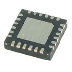
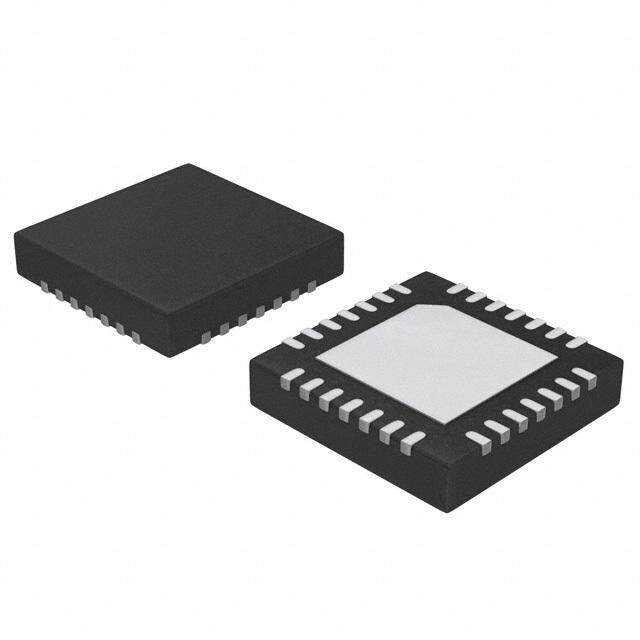
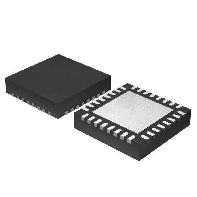
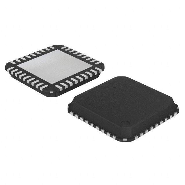
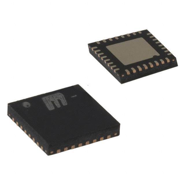
| 产品图片 |
|
| rohs | 符合RoHS无铅 / 符合限制有害物质指令(RoHS)规范要求 |
| 产品系列 | 接口 IC,输入/输出控制器接口集成电路,Silicon Labs CP2105-F01-GM- |
| 数据手册 | |
| 产品型号 | CP2105-F01-GMCP2105-F01-GM |
| 产品培训模块 | http://www.digikey.cn/PTM/IndividualPTM.page?site=cn&lang=zhs&ptm=25291 |
| 产品种类 | 输入/输出控制器接口集成电路 |
| 供应商器件封装 | 24-QFN(4x4) |
| 其它名称 | 336-2009-5 |
| 功能 | 桥,USB 至 UART |
| 包装 | 管件 |
| 协议 | USB |
| 单位重量 | 38.790 mg |
| 商标 | Silicon Labs |
| 安装风格 | SMD/SMT |
| 封装 | Tube |
| 封装/外壳 | 24-WFQFN 裸露焊盘 |
| 封装/箱体 | QFN-24 |
| 工作温度 | -40°C ~ 85°C |
| 工作电源电压 | 3.3 V |
| 工厂包装数量 | 91 |
| 接口 | UART |
| 最大工作温度 | + 85 C |
| 最小工作温度 | - 40 C |
| 标准 | USB 2.0 |
| 标准包装 | 91 |
| 电压-电源 | 1.8V,3 V ~ 3.6 V |
| 电流-电源 | 17mA |
| 系列 | CP2105 |
| 配用 | /product-detail/zh/CP2105EK/336-2005-ND/2486182 |


- 商务部:美国ITC正式对集成电路等产品启动337调查
- 曝三星4nm工艺存在良率问题 高通将骁龙8 Gen1或转产台积电
- 太阳诱电将投资9.5亿元在常州建新厂生产MLCC 预计2023年完工
- 英特尔发布欧洲新工厂建设计划 深化IDM 2.0 战略
- 台积电先进制程称霸业界 有大客户加持明年业绩稳了
- 达到5530亿美元!SIA预计今年全球半导体销售额将创下新高
- 英特尔拟将自动驾驶子公司Mobileye上市 估值或超500亿美元
- 三星加码芯片和SET,合并消费电子和移动部门,撤换高东真等 CEO
- 三星电子宣布重大人事变动 还合并消费电子和移动部门
- 海关总署:前11个月进口集成电路产品价值2.52万亿元 增长14.8%


PDF Datasheet 数据手册内容提取
CP2105 SINGLE-CHIP USB TO DUAL UART BRIDGE Single-Chip USB to Dual UART Data Transfer Standard UART Interface Features Integrated USB transceiver; no external resistors Data format: 8 data bits, 1 Stop bit required Parity: Even, Odd, No parity Integrated clock; no external crystal required Baud rates: 2400bps to 921600bps Integrated 296-Byte One-Time Programmable ROM for 288 Byte receive and transmit buffers storing customizable product information Three GPIO signals for status and control On-chip power-on reset circuit Virtual COM Port Device Drivers On-chip voltage regulator: 3.45V output Works with Existing COM Port PC Applications USB Peripheral Function Controller Royalty-Free Distribution License USB Specification 2.0 compliant; full-speed (12Mbps) Windows 7/Vista/XP/Server 2003/2000 USB Suspend states supported via SUSPEND pins Mac OS-X Two UART Interfaces (“Enhanced” and “Standard”) Linux Flow control options: USBXpress™ Direct Driver Support - Hardware (CTS / RTS) Royalty-Free Distribution License - Software (X-On / X-Off) - No flow control Windows 7/Vista/XP/Server 2003/2000 Configurable I/O (1.8V to VDD) using VIO pin Windows CE 6.0, 5.0, and 4.2 Configurable I/O (VDD to 5V) using external pull-up Supply Voltage All modem interface signals available (when GPIO is not Self-powered: 3.0 to 3.6V used) USB bus powered: 4.0 to 5.25V Enhanced UART Interface Features I/O voltage: 1.8V to VDD Data formats supported: Package - Data bits: 5, 6, 7, and 8 - Stop bits: 1, 1.5, and 2 RoHS-compliant 24-pin QFN (4 x 4mm) - Parity: odd, even, mark, space, no parity Ordering Part Number Baud rates: 300bps to 2.0Mbps 320 Byte receive and transmit buffers CP2105-F01-GM Two GPIO signals for status and control Temperature Range: –40 to +85°C RS-485 mode with bus transceiver control CP2105 Connect to VBUS or REGIN Voltage 48 MHz Baud Rate ECI Clock SUSPEND / RI_ECI External Supply VDD Regulator Oscillator Generator SCI Clock NC / DCD_ECI / VPP GPIO0_ECI / DTR_ECI GND Enhanced USB Interface GPIO.1_ECI / DSR_ECI USB GPIO / Handshake 6 UART Connector Control RTS_ECI and GPIO Data FIFOs CTS_ECI Signals VBUS VBUS Full-Speed Peripheral 320 B RX Enhanced UART RXD_ECI D+ D+ 12 Mbps Function 320 B TX (ECI) TXD_ECI D- D- Transceiver Controller GND 288 B RX Standard UART RXD_SCI 288 B TX (SCI) TXD_SCI 296 Byte PROM RTS_SCI (Product Customization) GPIO / Handshake 6 CTS_SCI Standard UART RST Control SUSPEND / RI_SCI and GPIO Signals GPIO.0_SCI / DCD_SCI Logic Level GPIO.1_SCI / DTR_SCI Supply VIO I/O Power and Logic Levels GPIO.2_SCI / DSR_SCI (1.8V to VDD) Figure 1. Example System Diagram Rev. 1.1 11/13 Copyright © 2013 by Silicon Laboratories CP2105
CP2105 2 Rev. 1.1
CP2105 TABLE OF CONTENTS Section Page 1. System Overview . . . . . . . . . . . . . . . . . . . . . . . . . . . . . . . . . . . . . . . . . . . . . . . . . . . . . . . . .4 2. Electrical Characteristics . . . . . . . . . . . . . . . . . . . . . . . . . . . . . . . . . . . . . . . . . . . . . . . . . .5 3. Pinout and Package Definitions . . . . . . . . . . . . . . . . . . . . . . . . . . . . . . . . . . . . . . . . . . . . .8 4. QFN-24 Package Specifications . . . . . . . . . . . . . . . . . . . . . . . . . . . . . . . . . . . . . . . . . . . .11 5. USB Function Controller and Transceiver . . . . . . . . . . . . . . . . . . . . . . . . . . . . . . . . . . . .13 6. Asynchronous Serial Data Bus (UART) Interfaces . . . . . . . . . . . . . . . . . . . . . . . . . . . . .13 6.1. ECI Baud Rate Generation . . . . . . . . . . . . . . . . . . . . . . . . . . . . . . . . . . . . . . . . . . . .14 7. GPIO Mode and Modem Mode . . . . . . . . . . . . . . . . . . . . . . . . . . . . . . . . . . . . . . . . . . . . . .14 8. GPIO Pins . . . . . . . . . . . . . . . . . . . . . . . . . . . . . . . . . . . . . . . . . . . . . . . . . . . . . . . . . . . . . .15 8.1. GPIO.0-1—Transmit and Receive Toggle . . . . . . . . . . . . . . . . . . . . . . . . . . . . . . . .15 8.2. GPIO.1_ECI—RS-485 Transceiver Bus Control . . . . . . . . . . . . . . . . . . . . . . . . . . . .16 8.3. Hardware Flow Control (RTS and CTS) . . . . . . . . . . . . . . . . . . . . . . . . . . . . . . . . . .17 9. One-Time Programmable ROM . . . . . . . . . . . . . . . . . . . . . . . . . . . . . . . . . . . . . . . . . . . . .18 10. Voltage Regulator . . . . . . . . . . . . . . . . . . . . . . . . . . . . . . . . . . . . . . . . . . . . . . . . . . . . . . .19 11. CP2105 Device Drivers . . . . . . . . . . . . . . . . . . . . . . . . . . . . . . . . . . . . . . . . . . . . . . . . . .21 11.1. Virtual COM Port Drivers . . . . . . . . . . . . . . . . . . . . . . . . . . . . . . . . . . . . . . . . . . . . .21 11.2. USBXpress Drivers . . . . . . . . . . . . . . . . . . . . . . . . . . . . . . . . . . . . . . . . . . . . . . . . .21 11.3. Driver Customization . . . . . . . . . . . . . . . . . . . . . . . . . . . . . . . . . . . . . . . . . . . . . . . .21 11.4. Driver Certification . . . . . . . . . . . . . . . . . . . . . . . . . . . . . . . . . . . . . . . . . . . . . . . . . .21 12. Relevant Application Notes . . . . . . . . . . . . . . . . . . . . . . . . . . . . . . . . . . . . . . . . . . . . . . .22 Document Change List . . . . . . . . . . . . . . . . . . . . . . . . . . . . . . . . . . . . . . . . . . . . . . . . . . . . .23 Contact Information . . . . . . . . . . . . . . . . . . . . . . . . . . . . . . . . . . . . . . . . . . . . . . . . . . . . . . . .24 Rev. 1.1 3
CP2105 1. System Overview The CP2105 is a highly integrated USB-to-Dual-UART Bridge Controller providing a simple solution for updating RS-232 designs to USB using a minimum of components and PCB space. The CP2105 includes a USB 2.0 full- speed function controller, USB transceiver, oscillator, one-time programmable ROM, and two asynchronous serial data buses (UART) with full modem control signals in a compact 4x4mm QFN-24 package (sometimes called “MLF” or “MLP”). The on-chip one-time programmable ROM may be used to customize the USB Vendor ID, Product ID, Product Description String, Power Descriptor, Device Release Number, Interface Strings, Device Serial Number, and Modem/GPIO configuration as desired for OEM applications. Royalty-free Virtual COM Port (VCP) device drivers provided by Silicon Labs allow a CP2105-based product to appear as two COM ports in PC applications. The CP2105 UART interfaces implement all RS-232 signals including control and handshaking, so existing system firmware does not need to be modified. The device also features a total of five GPIO signals that can be user-defined for status and control information. Support for I/O interface voltages down to 1.8V is provided via a V pin. Direct access driver support is also available through IO the Silicon Labs USBXpress driver set. See www.silabs.com for the latest application notes and product support information for the CP2105. An evaluation kit for the CP2105 (Part Number: CP2105EK) is available. It includes a CP2105-based USB-to- UART/RS-232 evaluation board, a complete set of VCP device drivers, USB and RS-232 cables, and full documentation. Contact a Silicon Labs sales representatives or go to www.silabs.com to order the CP2105 Evaluation Kit. 4 Rev. 1.1
CP2105 2. Electrical Characteristics Table 1. Absolute Maximum Ratings Parameter Test Condition Min Typ Max Unit Ambient Temperature Under Bias –55 — 125 °C Storage Temperature –65 — 150 °C Voltage on RST, GPIO or UART Pins with respect to V > 2.2V –0.3 — 5.8 V IO GND V < 2.2V –0.3 — V + IO IO 3.6 Voltage on VBUS with respect to GND V > 3.0V –0.3 — 5.8 V DD V not powered –0.3 — V + DD DD 3.6 Voltage on V or V with respect to GND –0.3 — 4.2 V DD IO Maximum Total Current through V , V , and GND — — 500 mA DD IO Maximum Output Current Sunk by RST or any I/O — — 100 mA pin Note: Stresses above those listed may cause permanent damage to the device. This is a stress rating only, and functional operation of the devices at or exceeding the conditions in the operation listings of this specification is not implied. Exposure to maximum rating conditions for extended periods may affect device reliability. Table 2. Global DC Electrical Characteristics V =3.0 to 3.6V, –40 to +85 °C unless otherwise specified. DD Parameter Test Condition Min Typ Max Unit Digital Supply Voltage (V ) 3.0 — 3.6 V DD Digital Port I/O Supply Voltage (V ) 1.8 — V V IO DD Voltage on V with respect to GND during a V > 3.3V 5.75 — V + V PP IO IO ROM programming operation 3.6 Capacitor on V for ROM programming — 4.7 — µF PP Supply Current1 Normal Operation; — 17 18.5 mA V Enabled REG Supply Current1 Suspended; — 100 220 µA V Enabled REG Supply Current - USB Pull-up2 — 200 228 µA Specified Operating Temperature Range –40 — +85 °C Notes: 1. If the device is connected to the USB bus, the USB Pull-up Current should be added to the supply current for total supply current. 2. The USB Pull-up supply current values are calculated values based on USB specifications. Rev. 1.1 5
CP2105 Table 3. UART and Suspend I/O DC Electrical Characteristics V =3.0 to 3.6V, V =1.8 V to V , –40 to +85°C unless otherwise specified. DD IO DD Parameters Test Condition Min Typ Max Unit Output High Voltage (V ) I =–10µA V –0.1 — — OH OH IO I =–3mA V –0.2 — — V OH IO I =–10mA — V –0.4 — OH IO Output Low Voltage (V ) I =10µA — — 0.1 OL OL I =8.5mA — — 0.4 V OL I =25mA — 0.6 — OL Input High Voltage (V ) 0.7 x V — — V IH IO Input Low Voltage (V ) — — 0.6 V IL Input Leakage Current Weak Pull-Up Off — — 1 µA Weak Pull-Up On, V =0V — 25 50 IO Maximum Input Voltage Open drain, logic high (1) — — 5.8 V Table 4. Reset Electrical Characteristics –40 to +85 °C unless otherwise specified. Parameter Test Condition Min Typ Max Unit RST Input High Voltage 0.75 x V — — V IO RST Input Low Voltage — — 0.6 V Minimum RST Low Time to 15 — — µs Generate a System Reset V Ramp Time for Power On — — 1 ms DD Table 5. Voltage Regulator Electrical Specifications –40 to +85°C unless otherwise specified. Parameter Test Condition Min Typ Max Units Input Voltage Range 3.0 — 5.25 V Output Voltage Output Current=1 to 100mA* 3.3 3.45 3.6 V VBUS Detection Input Threshold 2.5 — — V Bias Current — — 120 µA *Note: The maximum regulator supply current is 100mA. This includes the supply current of the CP2105. 6 Rev. 1.1
CP2105 Table 6. GPIO Output Specifications –40 to +85 °C unless otherwise specified. Parameter Test Condition Min Typ Max Unit RS-485 Active Time After Stop Bit — 1 — bit time* TX Toggle Rate — 7.5 — Hz RX Toggle Rate — 7.5 — Hz *Note: Bit-time is calculated as 1 / baud rate. Rev. 1.1 7
CP2105 3. Pinout and Package Definitions Table 7. CP2105 Pin Definitions Name Pin # Type Description V 6 Power In Power Supply Voltage Input. DD Power Out Voltage Regulator Output. See Section 10. V 5 Power In I/O Supply Voltage Input. IO GND 2 Ground. Must be tied to ground. RST 9 D I/O Device Reset. Open-drain output of internal POR or V monitor. An external DD source can initiate a system reset by driving this pin low for the time specified in Table4. REGIN 7 Power In 5V Regulator Input. This pin is the input to the on-chip voltage regulator. VBUS 8 D In VBUS Sense Input. This pin should be connected to the VBUS signal of a USB network. D+ 3 D I/O USB D+ D– 4 D I/O USB D– SUSPEND 1* D Out In GPIO mode, this pin indicates whether the device is in the USB Suspend or not. The polarity can be configured via the configuration PROM, and defaults to active-low. RI_SCI D In In modem control mode, this pin is the Ring Indicator control input (active low) for the Standard Comm Interface. GPIO.0_SCI 24* D I/O In GPIO mode, this pin is a user-configurable input or output for the Standard Comm Interface. DCD_SCI D In In modem control mode, this pin is the Data Carrier Detect control input (active low) for the Standard Comm Interface. GPIO.1_SCI 23* D I/O In GPIO mode, this pin is a user-configurable input or output for the Standard Comm Interface. DTR_SCI D Out In modem control mode, this pin is the Data Terminal Ready control output (active low) for the Standard Comm Interface. GPIO.2_SCI 22* D I/O In GPIO mode, this pin is a user-configurable input or output for the Standard Comm Interface. DSR_SCI D in In modem control mode, this pin is the Data Set Ready control input (active low) for the Standard Comm Interface. TXD_SCI 21 D Out Asynchronous data output (UART Transmit) for the Standard Comm Inter- face. RXD_SCI 20 D In Asynchronous data input (UART Receive) for the Standard Comm Interface. RTS_SCI 19* D Out Ready to Send control output (active low) for the Standard Comm Interface. *Note: Pins can be left unconnected when not used. 8 Rev. 1.1
CP2105 Table 7. CP2105 Pin Definitions (Continued) Name Pin # Type Description CTS_SCI 18* D In Clear To Send control input (active low) for the Standard Comm Interface. SUSPEND 17* D Out In GPIO mode, this pin indicates whether the device is in the USB Suspend or not. The polarity can be configured via the configuration PROM, and defaults to active-low. RI_ECI D In In modem control mode, this pin is the Ring Indicator control input (active low) for the Standard Comm Interface. NC 16* — In GPIO mode, this pin is not used. DCD_ECI D In In modem control mode, this pin is the Data Carrier Detect control input (active low) for the Enhanced Comm Interface. V Special Additionally, in either mode programming of the configuration ROM via the PP USB interface can be accomplished if a 4.7F capacitor is connected between this pin and GND. GPIO.0_ECI 15* D I/O In GPIO mode, this pin is a user-configurable input or output for the Enhanced Comm Interface. DTR_ECI D Out In modem control mode, this pin is the Data Terminal Ready control output (active low) for the Enhanced Comm Interface. GPIO.1_ECI 14* D I/O In GPIO mode, this pin is a user-configurable input or output for the Enhanced Comm Interface. DSR_ECI D in In modem control mode, this pin is the Data Set Ready control input (active low) for the Enhanced Comm Interface. TXD_ECI 13 D Out Asynchronous data output (UART Transmit) for the Enhanced Comm Inter- face. RXD_ECI 12 D In Asynchronous data input (UART Receive) for the Enhanced Comm Interface. RTS_ECI 11* D Out Ready to Send control output (active low) for the Enhanced Comm Interface. CTS_ECI 10* D In Clear To Send control input (active low) for the Enhanced Comm Interface. *Note: Pins can be left unconnected when not used. Rev. 1.1 9
CP2105 CI CI CI S S S _ _ _ D R R C T S D D D CI / CI / CI / _S _S _S CI CI CI 0 1 2 S S S O. O. O. _ _ _ PI PI PI XD XD TS G G G T R R 4 3 2 1 0 9 2 2 2 2 2 1 SUSPEND / RI_SCI 1 18 CTS_SCI GND 2 17 SUSPEND / RI_ECI D+ 3 CP2105-GM 16 NC / DCD_ECI / VPP Top View D- 4 15 GPIO.0_ECI / DTR_ECI VIO 5 14 GPIO.1_ECI / DSR_ECI GND (optional) VDD 6 13 TXD_ECI 7 8 9 10 11 12 N S T CI CI CI REGI VBU RS S_E S_E D_E T T X C R R Figure 2. QFN-24 Pinout Diagram (Top View) 10 Rev. 1.1
CP2105 4. QFN-24 Package Specifications Figure 3. QFN-24 Package Drawing Table 8. QFN-24 Package Dimensions Dimension Min Typ Max Dimension Min Typ Max A 0.70 0.75 0.80 L 0.30 0.40 0.50 A1 0.00 0.02 0.05 L1 0.00 — 0.15 b 0.18 0.25 0.30 aaa — — 0.15 D 4.00 BSC. bbb — — 0.10 D2 2.55 2.70 2.80 ddd — — 0.05 e 0.50 BSC. eee — — 0.08 E 4.00 BSC. Z — 0.24 — E2 2.55 2.70 2.80 Y — 0.18 — Notes: 1. All dimensions shown are in millimeters (mm) unless otherwise noted. 2. Dimensioning and Tolerancing per ANSI Y14.5M-1994. 3. This drawing conforms to JEDEC Solid State Outline MO-220, variation WGGD except for custom features D2, E2, Z, Y, and L, which are toleranced per supplier designation. 4. Recommended card reflow profile is per the JEDEC/IPC J-STD-020 specification for Small Body Components. Rev. 1.1 11
CP2105 Figure 4. QFN-24 Recommended PCB Land Pattern Table 9. QFN-24 PCB Land Pattern Dimensions Dimension Min Max Dimension Min Max C1 3.90 4.00 X2 2.70 2.80 C2 3.90 4.00 Y1 0.65 0.75 E 0.50 BSC Y2 2.70 2.80 X1 0.20 0.30 Notes: General 1. All dimensions shown are in millimeters (mm) unless otherwise noted. 2. This Land Pattern Design is based on the IPC-7351 guidelines. Solder Mask Design 3. All metal pads are to be non-solder mask defined (NSMD). Clearance between the solder mask and the metal pad is to be 60m minimum, all the way around the pad. Stencil Design 4. A stainless steel, laser-cut and electro-polished stencil with trapezoidal walls should be used to assure good solder paste release. 5. The stencil thickness should be 0.125mm (5 mils). 6. The ratio of stencil aperture to land pad size should be 1:1 for all perimeter pads. 7. A 2x2 array of 1.10 x 1.10mm openings on a 1.30mm pitch should be used for the center pad. Card Assembly 8. A No-Clean, Type-3 solder paste is recommended. 9. The recommended card reflow profile is per the JEDEC/IPC J-STD-020 specification for Small Body Components. 12 Rev. 1.1
CP2105 5. USB Function Controller and Transceiver The Universal Serial Bus (USB) function controller in the CP2105 is a USB 2.0 compliant full-speed device with integrated transceiver and on-chip matching and pullup resistors. The USB function controller manages all data transfers between the USB and the UARTs as well as command requests generated by the USB host controller and commands for controlling the function of the UARTs and GPIO pins. The USB Suspend and Resume states are supported for power management of both the CP2105 device as well as external circuitry. The CP2105 will enter Suspend mode when Suspend signaling is detected on the bus. On entering Suspend mode, the SUSPEND signals will be asserted if the corresponding interface is configured for GPIO mode. SUSPEND is also asserted after a CP2105 reset until device configuration during USB Enumeration is complete. SUSPEND is active-low by default, but can be configured using the PROM to be active high. The CP2105 exits the Suspend mode when any of the following occur: Resume signaling is detected or generated, a USB Reset signal is detected, or a device reset occurs. On exit of Suspend mode the SUSPEND signal is de- asserted. SUSPEND is weakly pulled to VIO in a high impedance state during a CP2105 reset. If this behavior is undesirable, a strong pulldown (10k) can be used to ensure SUSPEND remains low during reset. The logic level and output mode (push-pull or open-drain) of various pins during USB Suspend is configurable in the PROM. See Section 9 for more information. 6. Asynchronous Serial Data Bus (UART) Interfaces The CP2105 contains two UART interfaces, known as the Enhanced Communications Interface (ECI) and Standard Communications Interface (SCI) Each UART interface consists of the TXD (transmit) and RXD (receive) data signals as well as RTS and CTS flow control signals. Optionally, the modem control signals DSR, DTR, DCD, and RI can be enabled for each interface. If modem control signals are not required for the application, these pins can be configured to operate with alternate functions, such as GPIO and SUSPEND signals. The UARTs support RTS/CTS, DSR/DTR, and X-On/X-Off handshaking. The UARTs are programmable to support a variety of data formats and baud rates. The ECI supports several additional UART configuration options beyond those supported by the SCI. If the Virtual COM Port drivers are used, the data format and baud rate are set during COM port configuration on the PC. If the USBXpress drivers are used, the CP2105 is configured through the USBXpress API. The data formats and baud rates available to each interface are listed in Table10. Table 10. Data Formats and Baud Rates Interface Enhanced Communication Interface (ECI) Standard Communication Interface (SCI) Data Bits1 5, 6, 7, and 8 8 Stop Bits 1, 1.52, and 2 1 Parity Type None, Even, Odd, Mark, Space None, Even, Odd Baud Rate 2400, 4800, 7200, 9600, 14400, 19200, 28800, 300bps to 2.0Mbps3 38400, 56000, 57600, 115200, 128000, 230400, 460800, 921600 Notes: 1. Data sizes of 5 and 6 bits are not supported at baud rates above 921600bps. 2. 1.5 stop bits only available when using 5 data bits. 3. See “6.1. ECI Baud Rate Generation” for more details on possible baud rates for the ECI interface. Rev. 1.1 13
CP2105 6.1. ECI Baud Rate Generation The baud rate generator for the enhanced interface is very flexible, allowing the user to request any baud rate in the range from 300bps to 2.0Mbps. If the baud rate cannot be directly generated from the 48MHz oscillator, the device will choose the closest possible option. The actual baud rate is dictated by Equation1 and Equation2. 48MHz Prescale = 4 if Requested Baud Rate365 bps Clock Divider = ---------------------------------------------------------------------------------------------------- 2PrescaleRequested Baud Rate Prescale = 1 if Requested Baud Rate365 bps Equation1.Clock Divider Calculation 48MHz Prescale = 4 if Requested Baud Rate365 bps Actual Baud Rate = ----------------------------------------------------------------------------- 2PrescaleClock Divider Prescale = 1 if Requested Baud Rate365 bps Equation2.Baud Rate Calculation Most baud rates can be generated with an error of less than 1.0%. A general rule of thumb for the majority of UART applications is to limit the baud rate error on both the transmitter and the receiver to no more than ±2%. The clock divider value obtained in Equation1 is rounded to the nearest integer, which may produce an error source. Another error source will be the 48MHz oscillator, which is accurate to ±0.25%. Knowing the actual and requested baud rates, the total baud rate error can be found using Equation3. Baud Rate Error (%) = 1001–-------A----c---t-u----a---l- --B----a---u----d--- --R----a---t--e--------- 0.25% Requested Baud Rate Equation3.Baud Rate Error Calculation The UART also supports the transmission of a line break. The length of time for a line break is programmable from 1 to 125ms, or it can be set to transmit indefinitely until a stop command is sent from the application. 7. GPIO Mode and Modem Mode Each interface on the CP2105 can be configured in either GPIO Mode or Modem Mode. This allows the SCI and ECI to have either modem control signals or GPIO signals available at various pins. Table11 shows the functions that are available in each mode.By default, both interfaces are configured for GPIO Mode. Table 11. CP2105 Modem Mode and GPIO Mode Interface Pin # Modem Mode GPIO Mode 24 DCD_SCI GPIO_0_SCI Standard 23 DTR_SCI GPIO_1_SCI Communications Interface 22 DSR_SCI GPIO_2_SCI 1 RI_SCI SUSPEND_SCI 15 DTR_ECI GPIO_0_ECI Enhanced Communications 14 DSR_ECI GPIO_1_ECI Interface 17 RI_ECI SUSPEND_ECI Only one mode can be selected for each interface. Also, the mode of the CP2105 can only be configured once and cannot be reset to the default configuration after being programmed. Refer to “AN223: Runtime GPIO Control for CP210x” for more information on how to configure the port pins of the CP2105. 14 Rev. 1.1
CP2105 8. GPIO Pins The CP2105 supports five user-configurable GPIO pins for status and control information. The Standard Communication Interface (SCI) has three GPIO pins and the Enhanced Communication Interface (ECI) has two GPIO pins. To use the pins as GPIO pins, the interface with the GPIO pins must be configured in GPIO Mode. By default, both communication interfaces on the CP2105 are configured for GPIO Mode. If the Modem Control signals are needed, the interface must be configured for Modem Mode. See Section 7 for more information on Modem Mode. Each of these GPIO pins are usable as inputs, open-drain outputs, or push-pull outputs. Four of the GPIO pins also have alternate functions listed in Table12 (GPIO.2_SCI does not have an alternate function). Table 12. GPIO Mode Alternate Functions GPIO Pin Alternate Function GPIO.0_ECI TX Toggle GPIO.1_ECI RX Toggle/RS-485 Transceiver Control GPIO.0_SCI TX Toggle GPIO.1_SCI RX Toggle By default, all of the GPIO pins are configured as a GPIO input. The configuration of the pins is one-time programmable for each device. The difference between an open-drain output and a push-pull output is when the GPIO output is driven to logic high. A logic high, open-drain output pulls the pin to the VIO rail through an internal, pull-up resistor. A logic high, push-pull output directly connects the pin to the VIO voltage. Open-drain outputs are typically used when interfacing to logic at a higher voltage than the VIO pin. These pins can be safely pulled to the higher, external voltage through an external pull-up resistor. The maximum external pull-up voltage is 5V. The speed of reading and writing the GPIO pins is subject to the timing of the USB bus. GPIO pins configured as inputs or outputs are not recommended for real-time signalling. More information regarding the configuration and usage of these pins can be found in “AN721: CP21xx Device Customization Guide” and “AN223: Runtime GPIO Control for CP210x” available on the Silicon Labs website. 8.1. GPIO.0-1—Transmit and Receive Toggle GPIO.0 and GPIO.1 are configurable as Transmit Toggle and Receive Toggle pins for both the Enhanced Communication Interface and the Standard Communication Interface. These pins are logic high when a device is not transmitting or receiving data, and they toggle at a fixed rate as specified in Table6 when data transfer is in progress. Typically, these pins are connected to two LEDs to indicate data transfer. VIO CP2105 GPIO.0 – TX Toggle GPIO.1 – RX Toggle Figure 5. Transmit and Receive Toggle Typical Connection Diagram Rev. 1.1 15
CP2105 8.2. GPIO.1_ECI—RS-485 Transceiver Bus Control GPIO.1_ECI is configurable as an RS-485 bus transceiver control pin or the Enhanced Communication Interface which is connected to the DE and RE inputs of the transceiver. When configured for RS-485 mode, the pin is asserted during UART data transmission as well as line break transmission and the RX Toggle mode is not available. The RS-485 mode of GPIO.1_ECI is active-high by default, and is also configurable for active-low mode. CP2105 RS-485 Transceiver TX R RX D GPIO.1_ECI – RS485 RE DE Figure 6. RS-485 Transceiver Typical Connection Diagram 16 Rev. 1.1
CP2105 8.3. Hardware Flow Control (RTS and CTS) To utilize the functionality of the RTS and CTS pins of the CP2105, the device must be configured to use hardware flow control. RTS, or Ready To Send, is an active-low output from the CP2105 and indicates to the external UART device that the CP2105’s UART RX FIFO has not reached the watermark level of 191 bytes on the Enhanced Communication interface or 63 bytes on the Standard Communication Interface and is ready to accept more data. When the amount of data in the RX FIFO reaches the watermark, the CP2105 pulls RTS high to indicate to the external UART device to stop sending data. CTS, or Clear To Send, is an active-low input to the CP2105 and is used by the external UART device to indicate to the CP2105when the external UART device’s RX FIFO is getting full. The CP2105 will not send more than two bytes of data once CTS is pulled high. CP2105 RS232 System TX TX RX RX RTS RTS CTS CTS Figure 7. Hardware Flow Control Typical Connection Diagram Rev. 1.1 17
CP2105 9. One-Time Programmable ROM The CP2105 includes an internal one-time programmable ROM that may be used to customize the USB Vendor ID (VID), Product ID (PID), Product Description String, Power Descriptor, Device Release Number, Interface Strings, and Device Serial Number as desired for OEM applications. If the programmable ROM has not been programmed, the default configuration data shown in Table13 and Table14 is used. Table 13. Default USB Configuration Data Name Value Vendor ID 10C4h Product ID EA70h Power Descriptor (Attributes) 80h (Bus-powered) Power Descriptor (Max. Power) 32h (100 mA) Release Number 0100h (Release Version 01.00) Serial String Unique 8 character ASCII string (16 characters maximum) Product Description String “CP2105 USB to UART Bridge Controller” (47 characters maximum) ECI Interface String “Enhanced COM Port” (32 characters maximum) ECI Operating Mode GPIO mode SCI Interface String “Standard COM Port” (32 characters maximum) SCI Operating Mode GPIO mode Table 14. Default GPIO, UART, and Suspend Configuration Data Name Value GPIO.0_ECI/DTR_ECI GPIO Input GPIO.1_ECI/DSR_ECI GPIO Input GPIO.0_SCI/DCD_SCI GPIO Input GPIO.1_SCI/DTR_SCI GPIO Input GPIO.2_SCI/DSR_SCI GPIO Input Flush_Buffers Flush ECI and SCI TX and RX FIFO on open SUSPEND/RI_ECI Push-pull, Active-Low SUSPEND/RI_SCI Push-pull, Active-Low RS-485 Level Active-High While customization of the USB configuration data is optional, customizing the VID/PID combination is strongly recommended. A unique VID/PID combination will prevent the driver from conflicting with any other USB driver from a different manufacturer’s product. A vendor ID can be obtained from www.usb.org or Silicon Labs can provide a free PID for the OEM product that can be used with the Silicon Labs VID. Customizing the serial string for each individual device is also recommended if the OEM application is one in which it is possible for multiple CP210x-based devices to be connected to the same PC. The configuration data ROM can be programmed by Silicon Labs prior to shipment with the desired configuration information. It can also be programmed in-system over the USB interface by adding a capacitor to the PCB. If the configuration ROM is to be programmed in-system, a 4.7µF capacitor must be added between the NC/DCD_ECI/ VPP pin and ground. No other circuitry should be connected to NC/DCD_ECI/VPP during a programming operation, and V must remain at 3.3V or higher to successfully write to the configuration ROM. DD 18 Rev. 1.1
CP2105 10. Voltage Regulator The CP2105 includes an on-chip 5 to 3.45V voltage regulator. This allows the CP2105 to be configured as either a USB bus-powered device or a USB self-powered device. A typical connection diagram of the device in a bus- powered application using the regulator is shown in Figure8. When enabled, the voltage regulator output appears on the V pin and can be used to power external devices. See Table5 for the voltage regulator electrical DD characteristics. If it is desired to use the regulator to provide V in a self-powered application, the same connections from DD Figure8 can be used, but connect REGIN to an on-board 5V supply, and disconnect it from the VBUS pin. In addition, if REGIN may be unpowered while VBUS is 5V, a resistor divider shown in Note 5 of Figure9 is required to meet the absolute maximum voltage on VBUS specification in Table1. Note 2 VIO 4.7 k CP2105 Note 3 VIO RST SUSPEND / RI_ECI 3.45 V Power VDD NC / DCD_ECI / VPP Note 4 GPIO0_ECI / DTR_ECI 1-5 F 0.1 F Enhanced GPIO.1_ECI / DSR_ECI UART and GPIO RTS_ECI Signals REGIN CTS_ECI RXD_ECI 1 F TXD_ECI GND RXD_SCI USB TXD_SCI Connector RTS_SCI Standard VBUS VBUS CTS_SCI UART D+ D+ and GPIO SUSPEND / RI_SCI Signals D- D- GPIO.0_SCI / DCD_SCI GND GPIO.1_SCI / DTR_SCI GPIO.2_SCI / DSR_SCI Note 1 Note 1 : Avalanche transient voltage suppression diodes compatible with Full-speed USB should be added at the connector for ESD protection. Use Littelfuse p/n SP0503BAHT or equivalent. Note 2 : An external pull-up is not required, but can be added for noise immunity. Note 3 : VIO can be connected directly to VDD or to a supply as low as 1.8 V to set the I/O interface voltage. Note 4 : If configuration ROM is to be programmed via USB, a 4.7 F capacitor must be added between NC / DCD_ECI / VPP and ground. During a programming operation, the pin should not be connected to other circuitry, and VDD must be at least 3.3 V. Figure 8. Typical Bus-Powered Connection Diagram Rev. 1.1 19
CP2105 Alternatively, if 3.0 to 3.6V power is supplied to the V pin, the CP2105 can function as a USB self-powered DD device with the voltage regulator bypassed. For this configuration, the REGIN input should be tied to V to bypass DD the voltage regulator. A typical connection diagram showing the device in a self-powered application with the regulator bypassed is shown in Figure9. The USB max power and power attributes descriptor must match the device power usage and configuration. See application note “AN721: CP21xx Device Customization Guide” for information on how to customize USB descriptors for the CP2105. Note 2 VIO 4.7 k CP2105 Note 3 VIO RST SUSPEND / RI_ECI VDD NC / DCD_ECI / VPP Note 4 GPIO0_ECI / DTR_ECI 3.3 V Enhanced REGIN Power GPIO.1_ECI / DSR_ECI UART RTS_ECI and GPIO Signals CTS_ECI 1-5 F 0.1 F RXD_ECI TXD_ECI GND RXD_SCI TXD_SCI RTS_SCI Note 5 Standard (Optional) 24 k CTS_SCI UART USB VBUS SUSPEND / RI_SCI and GPIO Signals Connector 47 k GPIO.0_SCI / DCD_SCI VBUS GPIO.1_SCI / DTR_SCI D+ D+ GPIO.2_SCI / DSR_SCI D- D- GND Note 1 Note 1 : Avalanche transient voltage suppression diodes compatible with Full-speed USB should be added at the connector for ESD protection. Use Littelfuse p/n SP0503BAHT or equivalent. Note 2 : An external pull-up is not required, but can be added for noise immunity. Note 3 : VIO can be connected directly to VDD or to a supply as low as 1.8 V to set the I/O interface voltage. Note 4 : If configuration ROM is to be programmed via USB, a 4.7 F capacitor must be added between NC / DCD_ECI / VPP and ground. During a programming operation, the pin should not be connected to other circuitry, and VDD must be at least 3.3 V. Note 5 : For self-powered systems where VDD and VIO may be unpowered when VBUS is connected to 5 V, a resistor divider (or functionally-equivalent circuit) on VBUS is required to meet the absolute maximum voltage on VBUS specification in the Electrical Characteristics section. Figure 9. Typical Self-Powered Connection Diagram (Regulator Bypass) 20 Rev. 1.1
CP2105 11. CP2105 Device Drivers There are two sets of device drivers available for CP2105 devices: the Virtual COM Port (VCP) drivers and the USBXpress Direct Access drivers. Only one set of drivers is necessary to interface with the device. The latest drivers are available at http://www.silabs.com/products/mcu/Pages/SoftwareDownloads.aspx. 11.1. Virtual COM Port Drivers The CP2105 Virtual COM Port (VCP) device drivers allow a CP2105-based device to appear to the PC's application software as two COM ports. Application software running on the PC accesses the CP2105-based device as it would access two standard hardware COM ports. However, actual data transfer between the PC and the CP2105 device is performed over the USB interface. Therefore, existing COM port applications may be used to transfer data via the USB to the CP2105-based device without modifying the application. See application note “AN197: Serial Communications Guide for the CP210x” for Example Code for Interfacing to a CP2105 using the Virtual COM drivers. 11.2. USBXpress Drivers The Silicon Labs USBXpress drivers provide an alternate solution for interfacing with CP2105 devices. No serial port protocol expertise is required. Instead, a simple, high-level application program interface (API) is used to provide simpler CP210x connectivity and functionality. The USBXpress for CP210x Development Kit includes Windows device drivers, Windows device driver installer and uninstallers, and a host interface function library (host API) provided in the form of a Windows dynamic link library (DLL). The USBXpress driver set is recommended for new products that also include new PC software. The USBXpress interface is described in application note “AN169: USBXpress Programmer's Guide.” 11.3. Driver Customization In addition to customizing the device as described in "6. Asynchronous Serial Data Bus (UART) Interfaces" on page 13, the drivers and the drivers installation package can be also be customized. See application note “AN220: USB Driver Customization” for more information on generating customized VCP and USBXpress drivers. Important Note: The VID/PID in the drivers must match the VID/PID in the device for the drivers to load properly then the device is connected to the PC. 11.4. Driver Certification The default drivers for the CP2105 are Microsoft Windows Hardware Quality Labs (WHQL) certified. The certification means that the drivers have been tested by Microsoft and their latest operating systems will allow the drivers to be installed without any warnings or errors. The customized drivers that are generated using the AN220 software are not automatically certified. To become certified, they must go first through the Microsoft Driver Reseller Submission process. Contact Silicon Labs support for assistance with this process. Rev. 1.1 21
CP2105 12. Relevant Application Notes The following Application Notes are applicable to the CP2105. The latest versions of these application notes and their accompanying software are available at www.silabs.com/interface-appnotes. AN721: CP21xx Device Customization Guide. This application note describes how to use the AN721 software CP21xxCustomizationUtility to configure the USB parameters on the CP21xx devices. AN169: USBXpress Programmer's Guide. This application note describes the USBXpress API interface and includes example code. AN197: Serial Communications Guide for the CP210x. This application note describes how to use the standard Windows COM port function to communicate with the CP210x and includes example code. AN220: USB Driver Customization. This application note describes how to use the AN220 software to customize the VCP or USBXpress drivers with OEM information. AN223: Runtime GPIO Control for CP210x. This application note describes how to use the CP210xRuntime DLL to control the CP210x GPIO. 22 Rev. 1.1
CP2105 DOCUMENT CHANGE LIST Revision 0.1 to Revision 0.5 Updated ordering part number on page 1. Updated electrical specifications throughout Section 2. Added information on VPP pin in Section 3. Added Section 7. Updated Section 8. Updated Section 9. Revision 0.5 to Revision 1.0 Removed preliminary language. Revision 1.0 to Revision 1.1 Added a row for VBUS in Table1, “Absolute Maximum Ratings,” on page5. Added VDD Ramp Time for Power On specification to Table4, “Reset Electrical Characteristics,” on page6. Added VPP Voltage and Capacitor specifications to Table2, “Global DC Electrical Characteristics,” on page5. Updated AN144 references to AN721. Updated "10. Voltage Regulator" on page 19 to add absolute maximum voltage on VBUS requirements in self-powered systems. Rev. 1.1 23
Simplicity Studio One-click access to MCU and wireless tools, documentation, software, source code libraries & more. Available for Windows, Mac and Linux! IoT Portfolio SW/HW Quality Support and Community www.silabs.com/IoT www.silabs.com/simplicity www.silabs.com/quality community.silabs.com Disclaimer Silicon Labs intends to provide customers with the latest, accurate, and in-depth documentation of all peripherals and modules available for system and software implementers using or intending to use the Silicon Labs products. Characterization data, available modules and peripherals, memory sizes and memory addresses refer to each specific device, and "Typical" parameters provided can and do vary in different applications. Application examples described herein are for illustrative purposes only. Silicon Labs reserves the right to make changes without further notice and limitation to product information, specifications, and descriptions herein, and does not give warranties as to the accuracy or completeness of the included information. Silicon Labs shall have no liability for the consequences of use of the information supplied herein. This document does not imply or express copyright licenses granted hereunder to design or fabricate any integrated circuits. The products are not designed or authorized to be used within any Life Support System without the specific written consent of Silicon Labs. A "Life Support System" is any product or system intended to support or sustain life and/or health, which, if it fails, can be reasonably expected to result in significant personal injury or death. Silicon Labs products are not designed or authorized for military applications. Silicon Labs products shall under no circumstances be used in weapons of mass destruction including (but not limited to) nuclear, biological or chemical weapons, or missiles capable of delivering such weapons. Trademark Information Silicon Laboratories Inc.® , Silicon Laboratories®, Silicon Labs®, SiLabs® and the Silicon Labs logo®, Bluegiga®, Bluegiga Logo®, Clockbuilder®, CMEMS®, DSPLL®, EFM®, EFM32®, EFR, Ember®, Energy Micro, Energy Micro logo and combinations thereof, "the world’s most energy friendly microcontrollers", Ember®, EZLink®, EZRadio®, EZRadioPRO®, Gecko®, ISOmodem®, Precision32®, ProSLIC®, Simplicity Studio®, SiPHY®, Telegesis, the Telegesis Logo®, USBXpress® and others are trademarks or registered trademarks of Silicon Labs. ARM, CORTEX, Cortex-M3 and THUMB are trademarks or registered trademarks of ARM Holdings. Keil is a registered trademark of ARM Limited. All other products or brand names mentioned herein are trademarks of their respective holders. Silicon Laboratories Inc. 400 West Cesar Chavez Austin, TX 78701 USA http://www.silabs.com
Mouser Electronics Authorized Distributor Click to View Pricing, Inventory, Delivery & Lifecycle Information: S ilicon Laboratories: CP2105-F01-GM CP2105-F01-GMR