 Datasheet下载
- 型号: CP2102-GM
- 制造商: Silicon Laboratories
- 库位|库存: xxxx|xxxx
- 要求:
| 数量阶梯 | 香港交货 | 国内含税 |
| +xxxx | $xxxx | ¥xxxx |
查看当月历史价格
查看今年历史价格
CP2102-GM产品简介:
ICGOO电子元器件商城为您提供CP2102-GM由Silicon Laboratories设计生产,在icgoo商城现货销售,并且可以通过原厂、代理商等渠道进行代购。 CP2102-GM价格参考。Silicon LaboratoriesCP2102-GM封装/规格:接口 - 控制器, USB Bridge, USB to UART USB 2.0 UART Interface 28-QFN (5x5)。您可以下载CP2102-GM参考资料、Datasheet数据手册功能说明书,资料中有CP2102-GM 详细功能的应用电路图电压和使用方法及教程。
Silicon Labs的CP2102-GM是一款高度集成的USB转UART桥接控制器,广泛应用于需要将USB接口转换为串行通信(UART)的场景。其主要应用场景包括工业控制、消费电子、通信设备和嵌入式系统等。

在工业自动化领域,CP2102-GM常用于连接PLC、传感器、仪表与上位机,实现数据采集与监控。因其支持全速USB 2.0和标准UART信号,可方便地为不具备原生USB接口的微控制器添加USB通信功能。

在消费类电子产品中,该芯片被用于打印机、POS机、智能家居设备等,实现主机与设备之间的稳定串口通信。此外,在开发调试过程中,CP2102-GM也常作为MCU烧录或调试接口的USB转TTL模块核心芯片,因其驱动成熟、兼容性好、即插即用,深受工程师青睐。

通信设备如调制解调器、网络路由器中也采用该芯片进行内部模块间的数据传输。其小封装(QFN-28)、低功耗和高可靠性使其适用于空间受限且要求稳定的嵌入式环境。

CP2102-GM内置时钟电路,无需外部晶振,简化了设计,降低了成本。同时支持多种波特率配置,兼容Windows、macOS、Linux及Android系统,极大提升了应用灵活性。

总之,CP2102-GM凭借其高集成度、稳定性和易用性,成为USB转串口应用中的主流选择,广泛服务于各类需串行通信的设备与系统。
| 参数 | 数值 |
| 产品目录 | 集成电路 (IC)半导体 |
| 描述 | IC USB-TO-UART BRIDGE 28VQFN输入/输出控制器接口集成电路 USB to UART Bdg Chip |
| 产品分类 | |
| 品牌 | Silicon LabsSilicon Laboratories Inc |
| 产品手册 | |
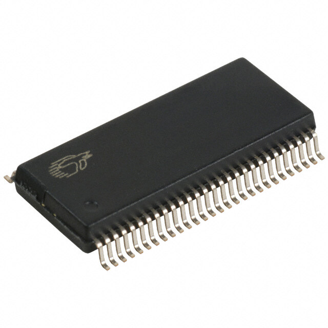
| 产品图片 |
|
| rohs | 符合RoHS无铅 / 符合限制有害物质指令(RoHS)规范要求 |
| 产品系列 | 接口 IC,输入/输出控制器接口集成电路,Silicon Labs CP2102-GM- |
| 数据手册 | |
| 产品型号 | CP2102-GMCP2102-GM |
| 产品培训模块 | http://www.digikey.cn/PTM/IndividualPTM.page?site=cn&lang=zhs&ptm=9298http://www.digikey.cn/PTM/IndividualPTM.page?site=cn&lang=zhs&ptm=25291 |
| 产品目录页面 | |
| 产品种类 | 输入/输出控制器接口集成电路 |
| 供应商器件封装 | 28-QFN(5x5) |
| 其它名称 | 336-1160 |
| 功能 | 桥,USB 至 UART |
| 包装 | 管件 |
| 协议 | USB |
| 单位重量 | 67.750 mg |
| 商标 | Silicon Labs |
| 安装风格 | SMD/SMT |
| 封装 | Tube |
| 封装/外壳 | 28-VFQFN 裸露焊盘 |
| 封装/箱体 | QFN-28 |
| 工作温度 | -40°C ~ 85°C |
| 工作电源电压 | 3.6 V |
| 工厂包装数量 | 73 |
| 接口 | UART |
| 最大工作温度 | + 125 C |
| 最小工作温度 | - 55 C |
| 标准 | USB 2.0 |
| 标准包装 | 73 |
| 电压-电源 | 3 V ~ 3.6 V |
| 电流-电源 | 20mA |
| 系列 | CP2102 |
| 配用 | /product-detail/zh/STEVAL-PCC018V1/497-14473-ND/4759345/product-detail/zh/CP2102EK/336-1161-ND/696599 |


- 商务部:美国ITC正式对集成电路等产品启动337调查
- 曝三星4nm工艺存在良率问题 高通将骁龙8 Gen1或转产台积电
- 太阳诱电将投资9.5亿元在常州建新厂生产MLCC 预计2023年完工
- 英特尔发布欧洲新工厂建设计划 深化IDM 2.0 战略
- 台积电先进制程称霸业界 有大客户加持明年业绩稳了
- 达到5530亿美元!SIA预计今年全球半导体销售额将创下新高
- 英特尔拟将自动驾驶子公司Mobileye上市 估值或超500亿美元
- 三星加码芯片和SET,合并消费电子和移动部门,撤换高东真等 CEO
- 三星电子宣布重大人事变动 还合并消费电子和移动部门
- 海关总署:前11个月进口集成电路产品价值2.52万亿元 增长14.8%


PDF Datasheet 数据手册内容提取
CP2102/9 SINGLE-CHIP USB-TO-UART BRIDGE For newer designs, the CP2102N devices offer compatible footprints and are recommended for use instead of the CP2102/9. See the Silicon Labs website (www.silabs.com/usbxpress) for more information. Single-Chip USB to UART Data Transfer Virtual COM Port Device Drivers - Integrated USB transceiver; no external resistors - Works with existing COM port PC Applications required - Royalty-free distribution license - Integrated clock; no external crystal required - Windows 8/7/Vista/Server 2003/XP/2000 - Internal 1024-byte programmable ROM for vendor ID, - Mac OS-X/OS-9 product ID, serial number, power descriptor, release - Linux number, and product description strings - EEPROM (CP2102) USBXpress™ Direct Driver Support - EPROM (One-time programmable) (CP2109) - Royalty-Free Distribution License - On-chip power-on reset circuit - Windows 7/Vista/XP/Server 2003/2000 - On-chip voltage regulator - Windows CE - 3.3V output (CP2102) - 3.45V output (CP2109) Example Applications - 100% pin and software compatible with CP2101 - Upgrade of RS-232 legacy devices to USB USB Function Controller - Cellular phone USB interface cable - USB interface cable - USB Specification 2.0 compliant; full-speed (12Mbps) - USB to RS-232 serial adapter - USB suspend states supported via SUSPEND pins Supply Voltage Asynchronous Serial Data BUS (UART) - Self-powered: 3.0 to 3.6V - All handshaking and modem interface signals - USB bus powered: 4.0 to 5.25V - Data formats supported: - Data bits: 5, 6, 7, and 8 Package - Stop bits: 1, 1.5, and 2 - Parity: odd, even, mark, space, no parity - RoHS-compliant 28-pin QFN (5x5mm) - Baud rates: 300bps to 1Mbps Ordering Part Numbers - 576 Byte receive buffer; 640 byte transmit buffer - Hardware or X-On/X-Off handshaking supported - CP2102-GM - Event character support - CP2109-A01-GM - Line break transmission Temperature Range: –40 to +85°C CP2102/9 VDD 7 Voltage REGIN IN Regulator 9 OUT RST (to external 12 circuitry for SUSPEND USB 3.3 – 3.45 V 6 11 suspend VDD SUSPEND states) 3 GND 2 RI 48 MHz 1 External 8 VBUS Oscillator DCD RS-232 USB 28 transceiver DTR CONNECTOR or UART 1 DSR 27 circuitry VBUS UART D- 2 5 D- USB USB Function TXD 26 GNDD+ 34 4 D+ Transceiver Controller RXD 25 640B 576B 24 1024B RTS 6 5 D1D2D3 PROM TX RX Buffer Buffer CTS 23 18 VPP *CP2109 only Figure1.Example System Diagram Rev. 1.8 1/17 Copyright © 2017 by Silicon Laboratories CP2102/9
CP2102/9 2 Rev. 1.8
CP2102/9 TABLE OF CONTENTS Section Page 1. System Overview . . . . . . . . . . . . . . . . . . . . . . . . . . . . . . . . . . . . . . . . . . . . . . . . . . . . . . . . .4 2. Ordering Information . . . . . . . . . . . . . . . . . . . . . . . . . . . . . . . . . . . . . . . . . . . . . . . . . . . . . .5 3. Electrical Specifications . . . . . . . . . . . . . . . . . . . . . . . . . . . . . . . . . . . . . . . . . . . . . . . . . . .6 4. Pinout and Package Definitions . . . . . . . . . . . . . . . . . . . . . . . . . . . . . . . . . . . . . . . . . . . .11 5. QFN-28 Package Specifications . . . . . . . . . . . . . . . . . . . . . . . . . . . . . . . . . . . . . . . . . . . .13 6. USB Function Controller and Transceiver . . . . . . . . . . . . . . . . . . . . . . . . . . . . . . . . . . . .15 7. Asynchronous Serial Data Bus (UART) Interface . . . . . . . . . . . . . . . . . . . . . . . . . . . . . .16 8. Internal Programmable ROM . . . . . . . . . . . . . . . . . . . . . . . . . . . . . . . . . . . . . . . . . . . . . . .17 9. CP2102/9 Device Drivers . . . . . . . . . . . . . . . . . . . . . . . . . . . . . . . . . . . . . . . . . . . . . . . . . .18 9.1. Virtual COM Port Drivers . . . . . . . . . . . . . . . . . . . . . . . . . . . . . . . . . . . . . . . . . . . . . .18 9.2. USBXpress Drivers . . . . . . . . . . . . . . . . . . . . . . . . . . . . . . . . . . . . . . . . . . . . . . . . . .18 9.3. Driver Customization . . . . . . . . . . . . . . . . . . . . . . . . . . . . . . . . . . . . . . . . . . . . . . . . .18 9.4. Driver Certification . . . . . . . . . . . . . . . . . . . . . . . . . . . . . . . . . . . . . . . . . . . . . . . . . . .18 10. Voltage Regulator . . . . . . . . . . . . . . . . . . . . . . . . . . . . . . . . . . . . . . . . . . . . . . . . . . . . . . .19 11. Porting Considerations from CP2102 to CP2109 . . . . . . . . . . . . . . . . . . . . . . . . . . . . .22 11.1. Pin-Compatibility . . . . . . . . . . . . . . . . . . . . . . . . . . . . . . . . . . . . . . . . . . . . . . . . . . .22 11.2. Distinguishing Factors . . . . . . . . . . . . . . . . . . . . . . . . . . . . . . . . . . . . . . . . . . . . . . .22 11.3. Differences in Electrical Specifications . . . . . . . . . . . . . . . . . . . . . . . . . . . . . . . . . .22 12. Relevant Application Notes . . . . . . . . . . . . . . . . . . . . . . . . . . . . . . . . . . . . . . . . . . . . . . .24 Document Change List . . . . . . . . . . . . . . . . . . . . . . . . . . . . . . . . . . . . . . . . . . . . . . . . . . . . .25 Rev. 1.8 3
CP2102/9 1. System Overview The CP2102/9 is a highly-integrated USB-to-UART Bridge Controller providing a simple solution for updating RS- 232 designs to USB using a minimum of components and PCB space. The CP2102/9 includes a USB 2.0 full- speed function controller, USB transceiver, oscillator, EEPROM or EPROM, and asynchronous serial data bus (UART) with full modem control signals in a compact 5 x 5mm QFN-28 package. No other external USB components are required. The on-chip programmable ROM may be used to customize the USB Vendor ID, Product ID, Product Description String, Power Descriptor, Device Release Number, and Device Serial Number as desired for OEM applications. The programmable ROM is programmed on-board via the USB, allowing the programming step to be easily integrated into the product manufacturing and testing process. Royalty-free Virtual COM Port (VCP) device drivers provided by Silicon Laboratories allow a CP2102/9-based product to appear as a COM port to PC applications. The CP2102/9 UART interface implements all RS-232 signals, including control and handshaking signals, so existing system firmware does not need to be modified. In many existing RS-232 designs, all that is required to update the design from RS-232 to USB is to replace the RS- 232 level-translator with the CP2102/9. Direct access driver support is available through the Silicon Laboratories USBXpress driver set. An evaluation kit for the CP2102 (Part Number: CP2102EK) is available. The kit includes a CP2102-based USB-to- UART/RS-232 evaluation board, a complete set of VCP device drivers, USB and RS-232 cables, and full documentation. Contact a Silicon Labs sales representative or go to www.silabs.com to order the CP2102 Evaluation Kit. The CP2102 Evaluation Kit serves as an evaluation kit for both the CP2102 and CP2109. 4 Rev. 1.8
CP2102/9 2. Ordering Information Table 1. Product Selection Guide Ordering Part Internal EEPROM EPROM Calibrated Supply Lead-free Package Number Programmable Internal Voltage (RoHS- ROM (Byte) 48MHz Regulator Compliant) Oscillator CP2102-GM* 1024 Y N Y Y Y QFN28 CP2109-A01-GM* 1024 N Y Y Y Y QFN28 *Note: Pin compatible with the CP2101-GM. Rev. 1.8 5
CP2102/9 3. Electrical Specifications Table 2. Absolute Maximum Ratings Parameter Symbol Test Condition Min Typ Max Unit Ambient Temperature under Bias T –55 — 125 °C BIAS Storage Temperature T –65 — 150 °C STG Voltage on V with respect to GND V –0.3 — 4.2 V DD DD Maximum Total Current through V — — 500 mA DD and GND Maximum Output Current sunk by — — 100 mA RST or any I/O pin CP2102 Voltage on any I/O Pin, VBUS, or RST –0.3 — 5.8 V with respect to GND CP2109 Voltage on any I/O Pin, VBUS, or RST V > 3.0 V –0.3 — 5.8 V DD with respect to GND V not powered –0.3 — V + DD DD 3.6 Note: Stresses above those listed may cause permanent device damage. This is a stress rating only, and functional operation of the devices at or exceeding the conditions in the operation listings of this specification is not implied. Exposure to maximum rating conditions for extended periods may affect device reliability. 6 Rev. 1.8
CP2102/9 Table 3. Recommended Operating Conditions V =3.0 to 3.6V, –40 to +85 °C unless otherwise specified DD Parameter Symbol Test Condition Min Typ Max Unit Supply Voltage V 3.0 3.3 3.6 V DD Supply Current - USB Pull-up1 I — 200 230 µA PU Specified Operating Temperature T –40 — +85 °C A Range Thermal Resistance2 θ — 32 — °C/W JA CP2102 Supply Current—Normal3 Normal Operation; — 20 26 mA V Enabled REG I Supply Current—Suspended3 REGIN Bus Powered; — 80 100 µA V Enabled REG CP2109 Supply Current—Normal3 Normal Operation; — 17 23 mA V Enabled REG I Supply Current—Suspended3 REGIN Bus Powered; — 90 230 µA V Enabled REG Notes: 1. The USB Pull-up supply current values are calculated values based on USB specifications. USB Pull-up supply current is current flowing from V to GND through USB pull-down/pull-up resistors on D+ and D-. DD 2. Thermal resistance assumes a multi-layer PCB with any exposed pad soldered to a PCB pad. 3. USB Pull-up current should be added for total supply current. Normal and suspended supply current is current flowing into V . Normal and suspended supply current is guaranteed by characterization. REGIN Rev. 1.8 7
CP2102/9 Table 4. UART and Suspend I/O DC Electrical Characteristics V =3.0 to 3.6V, –40 to +85°C unless otherwise specified DD Parameter Symbol Test Condition Min Typ Max Unit Baud Rate — — 921600 bps Input Leakage Current I — 25 50 µA L CP2102 Output High Voltage I =–10µA V –0.1 — — OH DD V I =–3mA V –0.7 — — V OH OH DD I =–10mA — V –0.8 — OH DD Output Low Voltage I =10µA — — 0.1 OL V I =8.5mA — — 0.6 V OL OL I =25mA — 1.0 — OL Input High Voltage V 2.0 — — V IH Input Low Voltage V — — 0.8 V IL CP2109 Output High Voltage I =–10µA V –0.1 — — OH DD V I =–3mA V –0.2 — — V OH OH DD I =–10mA — V –0.4 — OH DD Output Low Voltage I =10µA — — 0.1 OL V I =8.5mA — — 0.4 V OL OL I =25mA — 0.6 — OL Input High Voltage V 0.7 x V — — V IH DD Input Low Voltage V — — 0.6 V IL Table 5. Reset Electrical Characteristics –40 to +85 °C unless otherwise specified Parameter Symbol Test Condition Min Typ Max Unit V Ramp Time t Time to V ≥ 2.7 V — — 1 ms DD RMP DD RST Low Time to Generate a System t 15 — — µs RSTL Reset CP2102 RST Input High Voltage V 0.7 x V — — V IHRESET DD RST Input Low Voltage V — — 0.25 x V V ILRESET DD CP2109 RST Input High Voltage V 0.75 x V — — V IHRESET DD RST Input Low Voltage V — — 0.6 V ILRESET 8 Rev. 1.8
CP2102/9 Table 6. Voltage Regulator Electrical Specifications –40 to +85°C unless otherwise specified. Parameter Symbol Test Condition Min Typ Max Unit CP2102 Input Voltage Range V 4.0 — 5.25 V REGIN Output Voltage V Output Current=1 to 100mA* 3.0 3.3 3.6 V DDOUT VBUS Detection Input Threshold V 1.0 1.8 2.9 V VBUSTH Bias Current — 90 — µA CP2109 Input Voltage Range V 3.0 — 5.25 V REGIN Output Voltage V Output Current=1 to 100mA* 3.3 3.45 3.6 V DDOUT VBUS Detection Input Threshold V 2.5 — — V VBUSTH Bias Current — 83 99 µA *Note: The maximum regulator supply current is 100mA. Table 7. USB Transceiver Electrical Specifications V = 3.0 V to 3.6 V, –40 to +85°C unless otherwise specified. DD Parameter Symbol Test Condition Min Typ Max Unit Transmitter Output High Voltage V 2.8 — — V OH Output Low Voltage V — — 0.8 V OL Output Crossover Point V 1.3 — 2.0 V CRS Output Impedance (CP2102) Driving High — 38 — Driving Low — 38 — Z DRV Output Impedance (CP2109) Driving High — 36 — Driving Low — 36 — Pull-up Resistance R Full Speed (D+ Pull-up) 1.425 1.5 1.575 k PU Low Speed (D- Pull-up) Output Rise Time T Low Speed 75 — 300 ns R Full Speed 4 — 20 Output Fall Time T Low Speed 75 — 300 ns F Full Speed 4 — 20 Receiver Differential Input Sensitivity VDI | (D+) - (D-) | 0.2 — — V Differential Input Common VCM 0.8 — 2.5 V Mode Range Input Leakage Current IL Pullups Disabled — < 1.0 — µA *Note: Refer to the USB Specification for timing diagrams and symbol definitions. Rev. 1.8 9
CP2102/9 Table 8. EPROM Electrical Characteristics Parameter Test Condition Min Typ Max Unit CP2109 Voltage on V with respect to GND during a V > 3.3 V 5.75 — V + V PP DD DD ROM programming operation 3.6 Capacitor on V for In-system Programming — 4.7 — µF PP 10 Rev. 1.8
CP2102/9 4. Pinout and Package Definitions Table 9. CP2102/9 Pin Definitions Name Pin # Type Description V 6 Power In 3.0–3.6V Power Supply Voltage Input. DD Power Out 3.3V Voltage Regulator Output. See "10. Voltage Regulator" on page 19. GND 3 Ground RST 9 D I/O Device Reset. Open-drain output of internal POR or V monitor. An DD external source can initiate a system reset by driving this pin low for at least 15µs. REGIN 7 Power In 5V Regulator Input. This pin is the input to the on-chip voltage regu- lator. VBUS 8 D In VBUS Sense Input. This pin should be connected to the VBUS signal of a USB network. A 5V signal on this pin indicates a USB network connection. NC1 / This pin should be left unconnected or tied to V . This pin is unused DD on the CP2102 and may be connected to the Vpp programming 18 capacitor to maintain board compatibility with the CP2109. V 2 A Power V Programming Supply Voltage PP PP D+ 4 D I/O USB D+ D– 5 D I/O USB D– TXD 26 D Out Asynchronous data output (UART Transmit) RXD 25 D In Asynchronous data input (UART Receive) CTS 233 D In Clear To Send control input (active low) RTS 243 D Out Ready to Send control output (active low) DSR 273 D in Data Set Ready control input (active low) DTR 283 D Out Data Terminal Ready control output (active low) DCD 13 D In Data Carrier Detect control input (active low) RI 23 D In Ring Indicator control input (active low) SUSPEND 123 D Out This pin is driven high when the CP2102/9 enters the USB suspend state. SUSPEND 113 D Out This pin is driven low when the CP2102/9 enters the USB suspend state. NC 10, 13–22 These pins should be left unconnected or tied to V . DD Notes: 1. For CP2102, pin is no connect (NC). 2. For CP2109, pin is VPP. VPP can be left unconnected when not used for in-application programming. 3. Pins can be left unconnected when not used. Rev. 1.8 11
CP2102/9 R R D D S S T S X X T T C D D T R R C N 8 7 6 5 4 3 2 2 2 2 2 2 2 2 DCD 1 21 NC RI 2 20 NC GND 3 19 NC CP2102/9 D+ 4 18 NC / VPP Top View D- 5 17 NC V 6 16 NC DD GND REGIN 7 15 NC 8 9 10 11 12 13 14 S T C D D C C U S N N N N N B R E E V P P S S U U S S Figure2.QFN-28 Pinout Diagram (Top View) 12 Rev. 1.8
CP2102/9 5. QFN-28 Package Specifications Figure3.QFN-28 Package Drawing Table 10. QFN-28 Package Dimensions Dimension Min Typ Max Dimension Min Typ Max A 0.80 0.90 1.00 L 0.35 0.55 0.65 A1 0.00 0.02 0.05 L1 0.00 — 0.15 A3 0.25 REF aaa 0.15 b 0.18 0.23 0.30 bbb 0.10 D 5.00 BSC. ddd 0.05 D2 2.90 3.15 3.35 eee 0.08 e 0.50 BSC. Z 0.44 E 5.00 BSC. Y 0.18 E2 2.90 3.15 3.35 Notes: 1. All dimensions shown are in millimeters (mm) unless otherwise noted. 2. Dimensioning and Tolerancing per ANSI Y14.5M-1994. 3. This drawing conforms to the JEDEC Solid State Outline MO-220, variation VHHD except for custom features D2, E2, Z, Y, and L, which are toleranced per supplier designation. 4. Recommended card reflow profile is per the JEDEC/IPC J-STD-020 specification for Small Body Components. Rev. 1.8 13
CP2102/9 Figure4.QFN-28 Recommended PCB Land Pattern Table 11. QFN-28 PCB Land Pattern Dimensions Dimension Min Max Dimension Min Max C1 4.80 X2 3.20 3.30 C2 4.80 Y1 0.85 0.95 E 0.50 Y2 3.20 3.30 X1 0.20 0.30 Notes: General 1. All dimensions shown are in millimeters (mm) unless otherwise noted. 2. Dimensioning and Tolerancing is per the ANSI Y14.5M-1994 specification. 3. This Land Pattern Design is based on the IPC-7351 guidelines. Solder Mask Design 4. All metal pads are to be non-solder mask defined (NSMD). Clearance between the solder mask and the metal pad is to be 60µm minimum, all the way around the pad. Stencil Design 5. A stainless steel, laser-cut and electro-polished stencil with trapezoidal walls should be used to assure good solder paste release. 6. The stencil thickness should be 0.125mm (5mils). 7. The ratio of stencil aperture to land pad size should be 1:1 for all perimeter pins. 8. A 3x3 array of 0.90mm openings on a 1.1mm pitch should be used for the center pad to assure the proper paste volume (67% Paste Coverage). Card Assembly 9. A No-Clean, Type-3 solder paste is recommended. 10. The recommended card reflow profile is per the JEDEC/IPC J-STD-020 specification for Small Body Components. 14 Rev. 1.8
CP2102/9 6. USB Function Controller and Transceiver The Universal Serial Bus function controller in the CP2102/9 is a USB 2.0 compliant full-speed device with integrated transceiver and on-chip matching and pull-up resistors. The USB function controller manages all data transfers between the USB and the UART as well as command requests generated by the USB host controller and commands for controlling the function of the UART. The USB Suspend and Resume signals are supported for power management of both the CP2102/9 device as well as external circuitry. The CP2102/9 will enter Suspend mode when Suspend signaling is detected on the bus. On entering Suspend mode, the CP2102/9 asserts the SUSPEND and SUSPEND signals. SUSPEND and SUSPEND are also asserted after a CP2102/9 reset until device configuration during USB Enumeration is complete. The CP2102/9 exits Suspend mode when any of the following occur: (1) Resume signaling is detected or generated, (2) a USB Reset signal is detected, or (3) a device reset occurs. On exit of Suspend mode, the SUSPEND and SUSPEND signals are de-asserted. Both SUSPEND and SUSPEND temporarily float high during a CP2102/9 reset. If this behavior is undesirable, a strong pulldown (10k) can be used to ensure SUSPEND remains low during reset. See Figure5 for other recommended options. VDD CP2102/9 R1 4.7 k Option 1 7 REGIN C1 C2 9 RST 1.0 F 0.1 F (to external circuitry SUSPEND 12 for USB suspend states) 6 11 VDD SUSPEND C3 C4 R2 4.7 F 0.1 F Option 4 10 k 3 GND 2 RI Option 2 1 8 DCD External RS-232 VBUS USB 28 transceiver or DTR CONNECTOR UART circuitry 27 VBUS 1 DSR D- 2 5 D- TXD 26 D+ 3 GND 4 4 D+ RXD 25 24 RTS 6 5 D1 D2 D3 Option 3 CTS 23 18 VPP C5 4.7 F Option 5 Option 1: A 4.7 k pull-up resistor can be added to increase noise immunity. Option 2: A 4.7 µF capacitor can be added if powering other devices from the on-chip regulator. Option 3: Avalanche transient voltage suppression diodes should be added for ESD protection. Option 3: Use Littlefuse p/n SP0503BAHT or equivalent. Option 4: 10 k resistor to ground to hold SUSPEND low on initial power on or device reset. Option 5: A 4.7 µF capacitor can be added for in-system programming (CP2109 only). Figure5.Typical Connection Diagram Rev. 1.8 15
CP2102/9 7. Asynchronous Serial Data Bus (UART) Interface The CP2102/9 UART interface consists of the TX (transmit) and RX (receive) data signals as well as the RTS, CTS, DSR, DTR, DCD, and RI control signals. The UART supports RTS/CTS, DSR/DTR, and X-On/X-Off handshaking. The UART is programmable to support a variety of data formats and baud rates. If the Virtual COM Port drivers are used, the data format and baud rate are set during COM port configuration on the PC. If the USBXpress drivers are used, the CP2102/9 is configured through the USBXpress API. The data formats and baud rates available are listed in Table12. Table 12. Data Formats and Baud Rates Data Bits 5, 6, 7, and 8 Stop Bits 1, 1.51, and 2 Parity Type None, Even, Odd, Mark, Space Baud Rates2 300, 600, 1200, 1800, 2400, 4000, 4800, 7200, 9600, 14400, 16000, 19200, 28800, 38400, 51200, 56000, 57600, 64000, 76800, 115200, 128000, 153600, 230400, 250000, 256000, 460800, 500000, 576000, 9216003 Notes: 1. 5-bit only. 2. Additional baud rates are supported. See “AN721: CP210x/CP211x Device Customization Guide”. 3. 7 or 8 data bits only. 16 Rev. 1.8
CP2102/9 8. Internal Programmable ROM The CP2102 includes an internal electrically erasable programmable read-only memory (EEPROM), and the CP2109 includes an internal one-time programmable (OTP) erasable programmable read-only memory (EPROM). Either may be used to customize the USB Vendor ID (VID), Product ID (PID), Product Description String, Power Descriptor, Device Release Number and Device Serial Number as desired for OEM applications. If the EEPROM/ EPROM is not programmed with OEM data, the default configuration data shown in Table13 is used. The EEPROM has a typical endurance of 100,000 write cycles with a data retention of 100 years. The EPROM can only be written one time and cannot be erased. While customization of the USB configuration data is optional, it is recommended to customize the VID/PID combination. A unique VID/PID combination will prevent the driver from conflicting with any other USB driver. A vendor ID can be obtained from http://www.usb.org/ or Silicon Laboratories can provide a free PID for the OEM product that can be used with the Silicon Laboratories VID. It is also recommended to customize the serial number if the OEM application is one in which it is possible for multiple CP2102/9-based devices to be connected to the same PC. The internal programmable ROM is programmed via the USB. This allows the OEM's USB configuration data and serial number to be written to the CP2102/9 on-board ROM during the manufacturing and testing process. A stand- alone utility for programming the internal programmable ROM is available from Silicon Laboratories. A library of routines provided in the form of a Windows® DLL is also available. This library can be used to integrate the programmable ROM programming step into custom software used by the OEM to streamline testing and serial number management during manufacturing. USB descriptors can be locked to prevent future modification on the CP2102. The CP2109 can be programmed in- system over the USB interface by adding a capacitor to the PCB. If configuration ROM is to be programmed in- system, a 4.7μF capacitor must be added between the VPP pin and ground. No other circuitry should be connected to V during a programming operation, and V must remain at 3.3V or higher to successfully PP DD write to the configuration ROM. Table 13. Default USB Configuration Data Name Value Vendor ID 10C4h Product ID EA60h Power Descriptor (Attributes) 80h Power Descriptor 32h (Max. Power) Release Number 0100h CP2102 Serial Number 0001 (63 characters maximum) CP2109 Serial Number Unique 8 character ASCII string (63 characters maximum) CP2102 Product Description String “CP2102 USB to UART Bridge Controller” (126 characters maximum) CP2109 Product Description String “CP2109 USB to UART Bridge Controller” (126 characters maximum) Rev. 1.8 17
CP2102/9 9. CP2102/9 Device Drivers There are two sets of device drivers available for the CP2102/9 devices: the Virtual COM Port (VCP) drivers and the USBXpress Direct Access drivers. Only one set of drivers is necessary to interface with the device. The latest drivers are available at http://www.silabs.com/support/Pages/software-downloads.aspx. 9.1. Virtual COM Port Drivers The CP2102/9 Virtual COM Port (VCP) device drivers allow a CP2102/9-based device to appear to the PC's application software as a COM port. Application software running on the PC accesses the CP2102/9-based device as it would access a standard hardware COM port. However, actual data transfer between the PC and the CP2102/ 9 device is performed over the USB interface. Therefore, existing COM port applications may be used to transfer data via the USB to the CP2102/9-based device without modifying the application. See “AN197: Serial Communications Guide for the CP210x” for Example Code for Interfacing to a CP2102/9 using the Virtual COM drivers. 9.2. USBXpress Drivers The Silicon Laboratories USBXpress drivers provide an alternate solution for interfacing with CP2102/9 devices. No Serial Port protocol expertise is required. Instead, a simple, high-level application program interface (API) is used to provide simpler CP210x connectivity and functionality. The USBXpress for CP210x Development Kit includes Windows device drivers, Windows device driver installer and uninstallers, and a host interface function library (host API) provided in the form of a Windows Dynamic Link Library (DLL). The USBXpress driver set is recommended for new products that also include new PC software. The USBXpress interface is described in “AN169: USBXpress® Programmer's Guide.” 9.3. Driver Customization In addition to customizing the device as described in "8. Internal Programmable ROM" on page 17, the drivers and the drivers installation package can be also be customized. See “AN220: USB Driver Customization” for more information on generating customized VCP and USBXpress drivers. 9.4. Driver Certification The default drivers that are shipped with the CP2102/9 are Microsoft WHQL (Windows Hardware Quality Labs) certified. The certification means that the drivers have been tested by Microsoft and their latest operating systems (2000, Server 2003, XP, Vista, 7, and 8) will allow the drivers to be installed without any warnings or errors. Some installations of Windows will prevent unsigned drivers from being installed at all. The customized drivers that are generated using the AN220 software are not automatically certified. They must first go through the Microsoft Driver Reseller Submission process. Contact Silicon Laboratories support for assistance with this process. 18 Rev. 1.8
CP2102/9 10. Voltage Regulator The CP2102/9 includes an on-chip 5 to 3V voltage regulator. This allows the CP2102/9 to be configured as either a USB bus-powered device or a USB self-powered device. These configurations are shown in Figure6, Figure7, Figure8, Figure9, and Figure10. When enabled, the 3V voltage regulator output appears on the V pin and can DD be used to power external 3V devices. See Table6 for the voltage regulator electrical characteristics. Alternatively, if 3V power is supplied to the V pin, the CP2102/9 can function as a USB self-powered device with DD the voltage regulator disabled. For this configuration, it is recommended that the REGIN input be tied to the 3V net to disable the voltage regulator. In addition, if VDD or REGIN may be unpowered while VBUS is 5V, a resistor divider (or functionally-equivalent circuit) shown in Note 1 of Figure8 and Figure10 is required to meet the absolute maximum voltage on VBUS specification in Table2. The USB max power and power attributes descriptor must match the device power usage and configuration. See “AN721: CP210x/CP211x Device Customization Guide” for information on how to customize USB descriptors for the CP2102/9. Note: It is recommended to connect additional decoupling capacitance (e.g., 0.1µF in parallel with 1.0µF) to the REGIN input. CP2102/9 VBUS From VBUS VBUS Sense REGIN 5 V In Voltage Regulator (REG0) 1.0 F 0.1 F 3 V Out To 3 V VDD Device Power Net Power Net 4.7 F 0.1 F Figure6.Configuration 1: USB Bus-Powered Rev. 1.8 19
CP2102/9 CP2102 VBUS From VBUS VBUS Sense From 5 V REGIN 5 V In Voltage Regulator (REG0) Power Net 1.0 F 0.1 F 3 V Out To 3V VDD Device Power Net Power Net 4.7 F 0.1 F Figure7.CP2102 Configuration 2: USB Self-Powered CP2109 From VBUS 24 k VBUS Note 1 (Optional) 47 k VBUS Sense From 5 V REGIN 5 V In Voltage Regulator (REG0) Power Net 1.0 F 0.1 F 3 V Out To 3V VDD Device Power Net Power Net 4.7 F 0.1 F Note 1 : For self-powered systems where VDD or REGIN may be unpowered when VBUS is connected to 5 V, a resistor divider (or functionally-equivalent circuit) on VBUS is required to meet the absolute maximum voltage on VBUS specification in the Electrical Characteristics section. Figure8.CP2109 Configuration 2: USB Self-Powered 20 Rev. 1.8
CP2102/9 CP2102 VBUS From VBUS VBUS Sense REGIN 5 V In Voltage Regulator (REG0) 1.0 F 0.1 F 3 V Out From 3 V VDD Device Power Net Power Net 4.7 F 0.1 F Figure9.CP2102 Configuration 3: USB Self-Powered, Regulator Bypassed CP2109 From VBUS 24 k VBUS Note 1 (Optional) 47 k VBUS Sense REGIN 5 V In Voltage Regulator (REG0) 1.0 F 0.1 F 3 V Out From 3 V VDD Device Power Net Power Net 4.7 F 0.1 F Note 1 : For self-powered systems where VDD or REGIN may be unpowered when VBUS is connected to 5 V, a resistor divider (or functionally-equivalent circuit) on VBUS is required to meet the absolute maximum voltage on VBUS specification in the Electrical Characteristics section. Figure10.CP2109 Configuration 3: USB Self-Powered, Regulator Bypassed Rev. 1.8 21
CP2102/9 11. Porting Considerations from CP2102 to CP2109 This section highlights the differences between the CP2102 and CP2109. These devices are designed to be pin- compatible, and thus require very minor changes when porting hardware between devices. The CP2109 is an updated, cost-reduced version of the CP2102 with a one-time programmable ROM. 11.1. Pin-Compatibility The CP2109 is pin-compatible with the CP2102 with a single exception; the CP2109 requires an additional capacitor between V and GND for in-application programming. This capacitor is not required after the CP2109 PP EPROM has been successfully programmed or if the CP2109 does not need to be customized in system. 11.2. Distinguishing Factors The CP2102 has 1024 bytes of EEPROM for vendor ID (VID), product ID (PID), serial number, power descriptor, release number, and product description strings. This configuration EEPROM can be written and re-written multiple times. The CP2109 has 1024 bytes of one-time programmable EPROM for configuration. This configuration EPROM can only be written one time. The CP2109 may require an additional capacitor on V if in-application programming is desired. PP The CP2102 default serial number is always “0001”. Every CP2109 is programmed from the factory with a unique serial number. 11.3. Differences in Electrical Specifications Table14 and Table15 list differences in absolute maximum and electrical specifications between the CP2102 and CP2109. Refer to "3. Electrical Specifications" on page 6 for the comprehensive electrical specifications. Table 14. Differences in Absolute Maximum Specifications between CP2102 and CP2109 Parameter Symbol Test Condition CP2102 CP2109 Unit Voltage on any I/O Pin, VBUS, or RST with V > 3.0 V 5.8 5.8 V DD respect to GND, Maximum V not powered 5.8 V + 3.6 DD DD Table 15. Differences in Electrical Specifications between CP2102 and CP2109 Parameter Symbol Test Condition CP2102 CP2109 Unit Supply Current—Normal, Typical I Normal Operation; 20 17 mA REGIN V Enabled REG Supply Current—Normal, Maximum I Normal Operation; 26 23 mA REGIN V Enabled REG Supply Current—Suspended, Typical I Bus Powered; 80 90 µA REGIN V Enabled REG Supply Current—Suspended, Maximum I Bus Powered; 100 230 µA REGIN V Enabled REG Output High Voltage, Minimum V I =–3mA V –0.7 V –0.2 V OH OH DD DD Output High Voltage, Typical V I =–10mA V –0.8 V –0.4 V OH OH DD DD Output Low Voltage, Maximum V I =8.5mA 0.6 0.4 V OL OL Output Low Voltage, Typical V I =25mA 1.0 0.6 V OL OL Input High Voltage, Minimum V 2.0 0.7 x V V IH DD Input Low Voltage, Maximum V 0.8 0.6 V IL 22 Rev. 1.8
CP2102/9 Table 15. Differences in Electrical Specifications between CP2102 and CP2109 (Continued) Parameter Symbol Test Condition CP2102 CP2109 Unit RST Input High Voltage, Minimum V 0.7 x V 0.75 x V V IHRESET DD DD RST Input Low Voltage, Maximum V 0.25 x V 0.6 V ILRESET DD Regulator Input Voltage Range, Minimum V 4.0 3.0 V REGIN Regulator Output Voltage, Minimum V Output Current=1 3.0 3.3 V DDOUT to 100mA* Regulator Output Voltage, Typical V Output Current=1 3.3 3.45 V DDOUT to 100mA* VBUS Detection Input Threshold, Minimum V 1.0 2.5 V VBUSTH VBUS Detection Input Threshold, Typical V 1.8 — V VBUSTH VBUS Detection Input Threshold, Maximum V 2.9 — V VBUSTH Regulator Bias Current, Typical 90 83 µA Regulator Bias Current, Maximum — 99 µA USB Transceiver Output Impedance, Typical Z Driving High 38 36 Ω DRV Driving Low 38 36 Voltage on V with respect to GND during a V > 3.3 V — 5.75 V PP DD ROM programming operation, Minimum Voltage on V with respect to GND during a V > 3.3 V — V + 3.6 V PP DD DD ROM programming operation, Maximum Capacitor on V for In-application — 4.7 µF PP Programming, Typical Rev. 1.8 23
CP2102/9 12. Relevant Application Notes The following application notes are applicable to the CP2102/9. The latest versions of these application notes and their accompanying software are available at: http://www.silabs.com/products/mcu/Pages/ApplicationNotes.aspx. AN169: USBXpress® Programmer's Guide—This application note describes the USBXpress API interface and includes example code. AN197: Serial Communications Guide for the CP210x—This application note describes how to use the standard Windows COM port function to communicate with the CP2102/9 and includes example code. AN220: USB Driver Customization—This application note describes how to use the AN220 software to customize the VCP or USBXpress drivers with OEM information. AN721: CP210x/CP211x Device Customization Guide—This application note describes how to use the AN721 software to configure the USB parameters on the CP2102/9 devices. 24 Rev. 1.8
CP2102/9 DOCUMENT CHANGE LIST Updated Table6, added CP2109. Added Table7. Revision 1.0 to Revision 1.1 Added Table8. Updated Table9. Updated “Linux 2.40” bullet on page 1. - Updated pin 18 spec, Note 1, Note 2. Changed MLP to QFN throughout. Updated Figure2, added CP2109, pin 18. Revision 1.1 to Revision 1.2 Updated Section "6. USB Function Controller and Transceiver" on page 15, added CP2109. Added additional supported operating systems on Updated Figure5, added CP2109, Option 5. page 1. Updated Section "8. Internal Programmable ROM" Changed VDD conditions of Tables 3 and 4 from a on page 17, added CP2109. minimum of 2.7 to 3.0V. Updated Table12. Updated typical and max Supply Current number in - Updated Note 2 app note reference. Table 3. Updated Table13. Removed tantalum requirement in Figure5. - Added CP2109. Consolidated Sections 8 and 9. Updated Table15. Added Section "12. Relevant Application Notes" on - Updated normal maximum and suspended maximum page 24. supply current specs. Updated Section "10. Voltage Regulator" on page Revision 1.2 to Revision 1.3 19, changed AN144 to AN721. Added Section "11. Porting Considerations from Updated Figure1 on page 1. CP2102 to CP2109" on page 22. Updated Figure5 on page 15. Updated "11.2. Distinguishing Factors" on page 22. Updated Maximum VBUS Detection Input Threshold - Updated CP2102 default serial number to “0001”. in Table6 on page9. Updated Section "12. Relevant Application Notes" on page 24. Revision 1.3 to Revision 1.4 - Replaced AN144/AN205 with AN721. Updated Table 4 RST Input Low Voltage Revision 1.5 to Revision 1.6 Updated Table10, Note 4. Updated Table11, Note 10. Added mention of VBUS in Table2, “Absolute Maximum Ratings,” on page6 and split out port I/O Revision 1.4 to Revision 1.5 maximums for CP2102 and CP2109. Added CP2109. Added VPP voltage specifications to Table8, “EPROM Electrical Characteristics,” on page10. Updated Single-Chip USB to UART Data Transfer bullet on page 1. Updated "10. Voltage Regulator" on page 19 to add CP2109 absolute maximum voltage on VBUS Added CP2109 to Ordering Part Numbers on page requirements in self-powered systems. 1. Updated Section "1. System Overview" on page 4. Updated "11.3. Differences in Electrical Specifications" on page 22 to include the new or Updated Figure1. modified specifications. Added Section "2. Ordering Information" on page 5. Added Symbol columns to Tables in Section "3. Revision 1.6 to Revision 1.7 Electrical Specifications" on page 6. Added Note to front page. Updated Table3. - Added CP2109, Note 1, Note 2. Revision 1.7 to Revision 1.8 - Updated thermal resistance spec. - Updated normal supply current spec. January 20, 2017 Updated Table4, added CP2109, added Baud Rate. Revised front page note. Updated Table5, added CP2109, added VDD Ramp Time. Moved Table6. Rev. 1.8 25
Simplicity Studio One-click access to MCU and wireless tools, documentation, software, source code libraries & more. Available for Windows, Mac and Linux! IoT Portfolio SW/HW Quality Support and Community www.silabs.com/IoT www.silabs.com/simplicity www.silabs.com/quality community.silabs.com Disclaimer Silicon Labs intends to provide customers with the latest, accurate, and in-depth documentation of all peripherals and modules available for system and software implementers using or intending to use the Silicon Labs products. Characterization data, available modules and peripherals, memory sizes and memory addresses refer to each specific device, and "Typical" parameters provided can and do vary in different applications. Application examples described herein are for illustrative purposes only. Silicon Labs reserves the right to make changes without further notice and limitation to product information, specifications, and descriptions herein, and does not give warranties as to the accuracy or completeness of the included information. Silicon Labs shall have no liability for the consequences of use of the information supplied herein. This document does not imply or express copyright licenses granted hereunder to design or fabricate any integrated circuits. The products are not designed or authorized to be used within any Life Support System without the specific written consent of Silicon Labs. A "Life Support System" is any product or system intended to support or sustain life and/or health, which, if it fails, can be reasonably expected to result in significant personal injury or death. Silicon Labs products are not designed or authorized for military applications. Silicon Labs products shall under no circumstances be used in weapons of mass destruction including (but not limited to) nuclear, biological or chemical weapons, or missiles capable of delivering such weapons. Trademark Information Silicon Laboratories Inc.® , Silicon Laboratories®, Silicon Labs®, SiLabs® and the Silicon Labs logo®, Bluegiga®, Bluegiga Logo®, Clockbuilder®, CMEMS®, DSPLL®, EFM®, EFM32®, EFR, Ember®, Energy Micro, Energy Micro logo and combinations thereof, "the world’s most energy friendly microcontrollers", Ember®, EZLink®, EZRadio®, EZRadioPRO®, Gecko®, ISOmodem®, Precision32®, ProSLIC®, Simplicity Studio®, SiPHY®, Telegesis, the Telegesis Logo®, USBXpress® and others are trademarks or registered trademarks of Silicon Labs. ARM, CORTEX, Cortex-M3 and THUMB are trademarks or registered trademarks of ARM Holdings. Keil is a registered trademark of ARM Limited. All other products or brand names mentioned herein are trademarks of their respective holders. Silicon Laboratories Inc. 400 West Cesar Chavez Austin, TX 78701 USA http://www.silabs.com
Mouser Electronics Authorized Distributor Click to View Pricing, Inventory, Delivery & Lifecycle Information: S ilicon Laboratories: CP2102EK CP2102-GM CP2102-GMR CP2109-A01-GM CP2109-A01-GMR