 Datasheet下载
- 型号: USB4604-1080HN
- 制造商: Microchip
- 库位|库存: xxxx|xxxx
- 要求:
| 数量阶梯 | 香港交货 | 国内含税 |
| +xxxx | $xxxx | ¥xxxx |
查看当月历史价格
查看今年历史价格
USB4604-1080HN产品简介:
ICGOO电子元器件商城为您提供USB4604-1080HN由Microchip设计生产,在icgoo商城现货销售,并且可以通过原厂、代理商等渠道进行代购。 USB4604-1080HN价格参考。MicrochipUSB4604-1080HN封装/规格:接口 - 控制器, USB 集线器控制器 USB 2.0 USB 接口 48-SQFN(7x7)。您可以下载USB4604-1080HN参考资料、Datasheet数据手册功能说明书,资料中有USB4604-1080HN 详细功能的应用电路图电压和使用方法及教程。
Microchip Technology的USB4604-1080HN是一款接口控制器,主要应用于需要高性能USB连接和灵活配置的场景。以下是其典型应用场景:

1. 嵌入式系统:该控制器适用于工业控制、医疗设备和消费电子等领域的嵌入式系统中,提供稳定且高效的USB通信能力。

2. 人机界面(HMI)设备:如触摸屏、键盘、鼠标等外设,通过USB4604实现与主机之间的快速数据传输,支持多端口同步操作。

3. 音频/视频设备:用于音响系统、摄像头或其他多媒体设备中,确保高质量音视频流的实时传输。

4. 存储设备:在移动硬盘、U盘或SSD等外部存储装置上使用,提升文件读写速度并保证兼容性。

5. 网络通信设备:路由器、交换机等产品可利用此芯片增强其USB功能,方便连接各种外围设备。

6. 物联网(IoT)节点:作为智能传感器或执行器的一部分,帮助构建可靠的物联网解决方案,支持远程监控与管理。

7. 汽车电子:可用于车载信息娱乐系统及诊断工具中,满足汽车行业对可靠性和安全性的严格要求。

总之,USB4604-1080HN凭借其强大的性能和广泛的适应性,在众多需要高速USB连接的应用领域发挥着重要作用。
| 参数 | 数值 |
| 产品目录 | 集成电路 (IC)半导体 |
| 描述 | IC USB HUB/FLASH CTLR 48QFNUSB 接口集成电路 USB 2.0 Hi-Speed 4 Port Hub Controller |
| 产品分类 | |
| 品牌 | Microchip Technology |
| 产品手册 | |
| 产品图片 | |
| rohs | 符合RoHS无铅 / 符合限制有害物质指令(RoHS)规范要求 |
| 产品系列 | 接口 IC,USB 接口集成电路,Microchip Technology USB4604-1080HN- |
| 数据手册 | |
| 产品型号 | USB4604-1080HN |
| PCN组件/产地 | http://www.microchip.com/mymicrochip/NotificationDetails.aspx?id=5836&print=view |
| 产品种类 | USB 接口集成电路 |
| 商标 | Microchip Technology |
| 安装风格 | SMD/SMT |
| 封装 | Tray |
| 封装/箱体 | SQFN-48 |
| 工作电源电压 | 3.3 V |
| 工厂包装数量 | 260 |
| 接口类型 | I2C, SMBus, SPI, USB |
| 数据速率 | 480 Mbps |
| 最大工作温度 | + 70 C |
| 最小工作温度 | 0 C |
| 标准 | USB 2.0 |
| 标准包装 | 260 |
| 端口数量 | 4 Port |
| 类型 | Hub Controller |
| 速度 | High-Speed |


- 商务部:美国ITC正式对集成电路等产品启动337调查
- 曝三星4nm工艺存在良率问题 高通将骁龙8 Gen1或转产台积电
- 太阳诱电将投资9.5亿元在常州建新厂生产MLCC 预计2023年完工
- 英特尔发布欧洲新工厂建设计划 深化IDM 2.0 战略
- 台积电先进制程称霸业界 有大客户加持明年业绩稳了
- 达到5530亿美元!SIA预计今年全球半导体销售额将创下新高
- 英特尔拟将自动驾驶子公司Mobileye上市 估值或超500亿美元
- 三星加码芯片和SET,合并消费电子和移动部门,撤换高东真等 CEO
- 三星电子宣布重大人事变动 还合并消费电子和移动部门
- 海关总署:前11个月进口集成电路产品价值2.52万亿元 增长14.8%


PDF Datasheet 数据手册内容提取
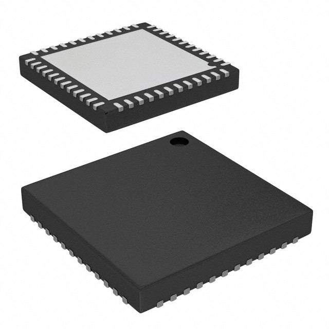
USB4604 USB 2.0 HSIC Hi-Speed 4-Port Hub Controller PRODUCT FEATURES Datasheet Highlights Additional Features Hub Controller IC with 4 downstream ports MultiTRAKTM High-Speed Inter-Chip (HSIC) support — Dedicated Transaction Translator per port — Upstream port selectable between HSIC or USB 2.0 PortMap USB-IF Battery Charger revision 1.2 support on up & — Configurable port mapping and disable sequencing downstream ports (DCP, CDP, SDP) PortSwap ® Battery charging support for Apple devices — Configurable differential intra-pair signal swapping FlexConnect: Downstream port 1 able to swap with PHYBoostTM — Programmable USB transceiver drive strength for upstream port, allowing master capable devices to recovering signal integrity control other devices on the hub USB to I2CTM/SPI bridge endpoint support V—ariPSreongsraemTmMable USB receiver sensitivity USB Link Power Management (LPM) support Low power operation SUSPEND pin for remote wakeup indication to host Full Power Management with individual or ganged Start Of Frame (SOF) synchronized clock output pin power control of each downstream port Vendor Specific Messaging (VSM) support Built-in Self-Powered or Bus-Powered internal default Enhanced OEM configuration options available settings provide flexibility in the quantity of USB through OTP or SMBus Slave Port expansion ports utilized without redesign Flexible power rail support Supports “Quad Page” configuration OTP flash — VBUS or VBAT only operation — Four consecutive 200 byte configuration pages — 3.3V only operation Fully integrated USB termination and Pull-up/Pull- — VBAT + 1.8V operation down resistors — 3.3V + 1.8V operation On-chip Power On Reset (POR) 48-pin (7x7mm) SQFN, RoHS compliant package Internal 3.3V and 1.2V voltage regulators Target Applications On Board 24MHz Crystal Driver, Resonator, or External 24MHz clock input LCD monitors and TVs USB host/device speed indicator. Per-port 3-color Multi-function USB peripherals LED drivers indicate the speed of USB host and PC mother boards device connection - hi-speed (480 Mbps), full-speed Set-top boxes, DVD players, DVR/PVR (12 Mbps), low-speed (1.5 Mbps) Printers and scanners Environmental PC media drive bay — Commercial temperature range support (0ºC to 70ºC) — Industrial temperature range support (-40ºC to 85ºC) Portable hub boxes Mobile PC docking Embedded systems 2014 Microchip Technology Inc. DS00001716A-page 1
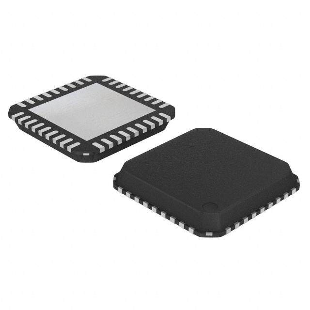
USB 2.0 HSIC Hi-Speed 4-Port Hub Controller Datasheet Order Number(s): TEMPERATURE ORDER NUMBER RANGE PACKAGE TYPE USB4604-1080HN (Hub Controller Enabled) 0°C to +70°C 48-pin SQFN USB4604-1070HN (Hub Controller Disabled) USB4604-1080HN-TR (Hub Controller Enabled) 48-pin SQFN 0°C to +70°C (Tape & Reel) USB4604-1070HN-TR (Hub Controller Disabled) USB4604i-1080HN (Hub Controller Enabled) -40°C to +85°C 48-pin SQFN USB4604i-1070HN (Hub Controller Disabled) USB4604i-1080HN-TR (Hub Controller Enabled) 48-pin SQFN -40°C to +85°C (Tape & Reel) USB4604i-1070HN-TR (Hub Controller Disabled) This product meets the halogen maximum concentration values per IEC61249-2-21 The table above represents valid part numbers at the time of printing and may not represent parts that are currently available. For the latest list of valid ordering numbers for this product, please contact the nearest sales office. TO OUR VALUED CUSTOMERS It is our intention to provide our valued customers with the best documentation possible to ensure successful use of your Microchip products. To this end, we will continue to improve our publications to better suit your needs. Our publications will be refined and enhanced as new volumes and updates are introduced. If you have any questions or comments regarding this publication, please contact the Marketing Communications Department via E-mail at docerrors@microchip.com. We welcome your feedback. Most Current Data Sheet To obtain the most up-to-date version of this data sheet, please register at our Worldwide Web site at: http://www.microchip.com You can determine the version of a data sheet by examining its literature number found on the bottom outside corner of any page. The last character of the literature number is the version number, (e.g., DS30000000A is version A of document DS30000000). Errata An errata sheet, describing minor operational differences from the data sheet and recommended workarounds, may exist for cur- rent devices. As device/documentation issues become known to us, we will publish an errata sheet. The errata will specify the revision of silicon and revision of document to which it applies. To determine if an errata sheet exists for a particular device, please check with one of the following: • Microchip’s Worldwide Web site; http://www.microchip.com • Your local Microchip sales office (see last page) When contacting a sales office, please specify which device, revision of silicon and data sheet (include -literature number) you are using. Customer Notification System Register on our web site at www.microchip.com to receive the most current information on all of our products. DS00001716A-page 2 2014 Microchip Technology Inc.
USB 2.0 HSIC Hi-Speed 4-Port Hub Controller Datasheet Table of Contents Chapter1 General Description . . . . . . . . . . . . . . . . . . . . . . . . . . . . . . . . . . . . . . . . . . . . . . . . . . 7 1.1 Block Diagram. . . . . . . . . . . . . . . . . . . . . . . . . . . . . . . . . . . . . . . . . . . . . . . . . . . . . . . . . . . . . . . . . . . . 9 Chapter2 Acronyms and Definitions . . . . . . . . . . . . . . . . . . . . . . . . . . . . . . . . . . . . . . . . . . . . 10 2.1 Acronyms. . . . . . . . . . . . . . . . . . . . . . . . . . . . . . . . . . . . . . . . . . . . . . . . . . . . . . . . . . . . . . . . . . . . . . . 10 2.2 Reference Documents. . . . . . . . . . . . . . . . . . . . . . . . . . . . . . . . . . . . . . . . . . . . . . . . . . . . . . . . . . . . . 10 Chapter3 Pin Descriptions . . . . . . . . . . . . . . . . . . . . . . . . . . . . . . . . . . . . . . . . . . . . . . . . . . . . 11 3.1 Pin Descriptions. . . . . . . . . . . . . . . . . . . . . . . . . . . . . . . . . . . . . . . . . . . . . . . . . . . . . . . . . . . . . . . . . . 12 3.2 Pin Assignments . . . . . . . . . . . . . . . . . . . . . . . . . . . . . . . . . . . . . . . . . . . . . . . . . . . . . . . . . . . . . . . . . 21 3.3 Buffer Type Descriptions. . . . . . . . . . . . . . . . . . . . . . . . . . . . . . . . . . . . . . . . . . . . . . . . . . . . . . . . . . . 22 Chapter4 Power Connections. . . . . . . . . . . . . . . . . . . . . . . . . . . . . . . . . . . . . . . . . . . . . . . . . . 23 4.1 Integrated Power Regulators. . . . . . . . . . . . . . . . . . . . . . . . . . . . . . . . . . . . . . . . . . . . . . . . . . . . . . . . 23 4.1.1 3.3V Regulator. . . . . . . . . . . . . . . . . . . . . . . . . . . . . . . . . . . . . . . . . . . . . . . . . . . . . . . . . . . . 23 4.1.2 1.2V Regulator. . . . . . . . . . . . . . . . . . . . . . . . . . . . . . . . . . . . . . . . . . . . . . . . . . . . . . . . . . . . 23 4.2 Power Configurations . . . . . . . . . . . . . . . . . . . . . . . . . . . . . . . . . . . . . . . . . . . . . . . . . . . . . . . . . . . . . 23 4.2.1 Single Supply Configurations. . . . . . . . . . . . . . . . . . . . . . . . . . . . . . . . . . . . . . . . . . . . . . . . . 23 4.2.2 Dual Supply Configurations. . . . . . . . . . . . . . . . . . . . . . . . . . . . . . . . . . . . . . . . . . . . . . . . . . 24 4.3 Power Connection Diagrams. . . . . . . . . . . . . . . . . . . . . . . . . . . . . . . . . . . . . . . . . . . . . . . . . . . . . . . . 25 Chapter5 Modes of Operation . . . . . . . . . . . . . . . . . . . . . . . . . . . . . . . . . . . . . . . . . . . . . . . . . 26 5.1 Boot Sequence . . . . . . . . . . . . . . . . . . . . . . . . . . . . . . . . . . . . . . . . . . . . . . . . . . . . . . . . . . . . . . . . . . 28 5.1.1 Standby Mode . . . . . . . . . . . . . . . . . . . . . . . . . . . . . . . . . . . . . . . . . . . . . . . . . . . . . . . . . . . . 28 5.1.2 Hardware Initialization Stage (HW_INIT). . . . . . . . . . . . . . . . . . . . . . . . . . . . . . . . . . . . . . . . 28 5.1.3 Software Initialization Stage (SW_INIT). . . . . . . . . . . . . . . . . . . . . . . . . . . . . . . . . . . . . . . . 28 5.1.4 SOC Configuration Stage (SOC_CFG). . . . . . . . . . . . . . . . . . . . . . . . . . . . . . . . . . . . . . . . . 28 5.1.5 Configuration Stage (CONFIG) . . . . . . . . . . . . . . . . . . . . . . . . . . . . . . . . . . . . . . . . . . . . . . . 28 5.1.6 Battery Charger Detection Stage (CHGDET) . . . . . . . . . . . . . . . . . . . . . . . . . . . . . . . . . . . . 29 5.1.7 Hub Connect Stage (Hub.Connect). . . . . . . . . . . . . . . . . . . . . . . . . . . . . . . . . . . . . . . . . . . . 29 5.1.8 Normal Mode. . . . . . . . . . . . . . . . . . . . . . . . . . . . . . . . . . . . . . . . . . . . . . . . . . . . . . . . . . . . . 29 Chapter6 Device Configuration . . . . . . . . . . . . . . . . . . . . . . . . . . . . . . . . . . . . . . . . . . . . . . . . 30 6.1 Configuration Method Selection . . . . . . . . . . . . . . . . . . . . . . . . . . . . . . . . . . . . . . . . . . . . . . . . . . . . . 30 6.2 Customer Accessible Functions . . . . . . . . . . . . . . . . . . . . . . . . . . . . . . . . . . . . . . . . . . . . . . . . . . . . . 30 6.2.1 USB Accessible Functions. . . . . . . . . . . . . . . . . . . . . . . . . . . . . . . . . . . . . . . . . . . . . . . . . . . 30 6.2.2 SMBus Accessible Functions . . . . . . . . . . . . . . . . . . . . . . . . . . . . . . . . . . . . . . . . . . . . . . . . 32 6.3 Device Configuration Straps . . . . . . . . . . . . . . . . . . . . . . . . . . . . . . . . . . . . . . . . . . . . . . . . . . . . . . . . 32 6.3.1 Port Disable (PRT_DIS_Mx/PRT_DIS_Px). . . . . . . . . . . . . . . . . . . . . . . . . . . . . . . . . . . . . . 33 6.3.2 SPI Speed Select (SPI_SPD_SEL). . . . . . . . . . . . . . . . . . . . . . . . . . . . . . . . . . . . . . . . . . . . 33 Chapter7 Device Interfaces. . . . . . . . . . . . . . . . . . . . . . . . . . . . . . . . . . . . . . . . . . . . . . . . . . . . 34 7.1 SPI Interface . . . . . . . . . . . . . . . . . . . . . . . . . . . . . . . . . . . . . . . . . . . . . . . . . . . . . . . . . . . . . . . . . . . . 34 7.1.1 Operation of the Hi-Speed Read Sequence . . . . . . . . . . . . . . . . . . . . . . . . . . . . . . . . . . . . . 34 7.1.2 Operation of the Dual High Speed Read Sequence . . . . . . . . . . . . . . . . . . . . . . . . . . . . . . . 35 7.1.3 32 Byte Cache. . . . . . . . . . . . . . . . . . . . . . . . . . . . . . . . . . . . . . . . . . . . . . . . . . . . . . . . . . . . 35 7.1.4 Interface Operation to the SPI Port When Not Performing Fast Reads. . . . . . . . . . . . . . . . . 35 7.1.5 Erase Example . . . . . . . . . . . . . . . . . . . . . . . . . . . . . . . . . . . . . . . . . . . . . . . . . . . . . . . . . . . 36 2014 Microchip Technology Inc. DS00001716A-page 3
USB 2.0 HSIC Hi-Speed 4-Port Hub Controller Datasheet 7.1.6 Byte Program Example . . . . . . . . . . . . . . . . . . . . . . . . . . . . . . . . . . . . . . . . . . . . . . . . . . . . . 37 7.1.7 Command Only Program Example . . . . . . . . . . . . . . . . . . . . . . . . . . . . . . . . . . . . . . . . . . . . 38 7.1.8 JEDEC-ID Read Example . . . . . . . . . . . . . . . . . . . . . . . . . . . . . . . . . . . . . . . . . . . . . . . . . . . 39 7.2 I2C Master Interface . . . . . . . . . . . . . . . . . . . . . . . . . . . . . . . . . . . . . . . . . . . . . . . . . . . . . . . . . . . . . . 39 7.2.1 I2C Message Format. . . . . . . . . . . . . . . . . . . . . . . . . . . . . . . . . . . . . . . . . . . . . . . . . . . . . . . 39 7.2.2 Pull-Up Resistors for I2C. . . . . . . . . . . . . . . . . . . . . . . . . . . . . . . . . . . . . . . . . . . . . . . . . . . . 41 7.3 SMBus Slave Interface . . . . . . . . . . . . . . . . . . . . . . . . . . . . . . . . . . . . . . . . . . . . . . . . . . . . . . . . . . . . 41 Chapter8 Functional Descriptions. . . . . . . . . . . . . . . . . . . . . . . . . . . . . . . . . . . . . . . . . . . . . . 42 8.1 Battery Charger Detection & Charging . . . . . . . . . . . . . . . . . . . . . . . . . . . . . . . . . . . . . . . . . . . . . . . . 42 8.1.1 Upstream Battery Charger Detection. . . . . . . . . . . . . . . . . . . . . . . . . . . . . . . . . . . . . . . . . . . 42 8.1.2 Downstream Battery Charging. . . . . . . . . . . . . . . . . . . . . . . . . . . . . . . . . . . . . . . . . . . . . . . . 43 8.2 SOF Clock Output. . . . . . . . . . . . . . . . . . . . . . . . . . . . . . . . . . . . . . . . . . . . . . . . . . . . . . . . . . . . . . . . 45 8.3 Flex Connect. . . . . . . . . . . . . . . . . . . . . . . . . . . . . . . . . . . . . . . . . . . . . . . . . . . . . . . . . . . . . . . . . . . . 45 8.3.1 Port Control . . . . . . . . . . . . . . . . . . . . . . . . . . . . . . . . . . . . . . . . . . . . . . . . . . . . . . . . . . . . . . 45 8.4 Resets. . . . . . . . . . . . . . . . . . . . . . . . . . . . . . . . . . . . . . . . . . . . . . . . . . . . . . . . . . . . . . . . . . . . . . . . . 46 8.4.1 Power-On Reset (POR). . . . . . . . . . . . . . . . . . . . . . . . . . . . . . . . . . . . . . . . . . . . . . . . . . . . . 46 8.4.2 External Chip Reset (RESET_N). . . . . . . . . . . . . . . . . . . . . . . . . . . . . . . . . . . . . . . . . . . . . . 46 8.4.3 USB Bus Reset . . . . . . . . . . . . . . . . . . . . . . . . . . . . . . . . . . . . . . . . . . . . . . . . . . . . . . . . . . . 46 8.5 Link Power Management (LPM) . . . . . . . . . . . . . . . . . . . . . . . . . . . . . . . . . . . . . . . . . . . . . . . . . . . . . 46 8.6 Suspend (SUSPEND) . . . . . . . . . . . . . . . . . . . . . . . . . . . . . . . . . . . . . . . . . . . . . . . . . . . . . . . . . . . . . 47 Chapter9 Operational Characteristics. . . . . . . . . . . . . . . . . . . . . . . . . . . . . . . . . . . . . . . . . . . 48 9.1 Absolute Maximum Ratings*. . . . . . . . . . . . . . . . . . . . . . . . . . . . . . . . . . . . . . . . . . . . . . . . . . . . . . . . 48 9.2 Operating Conditions** . . . . . . . . . . . . . . . . . . . . . . . . . . . . . . . . . . . . . . . . . . . . . . . . . . . . . . . . . . . . 49 9.3 Power Consumption . . . . . . . . . . . . . . . . . . . . . . . . . . . . . . . . . . . . . . . . . . . . . . . . . . . . . . . . . . . . . . 50 9.3.1 Operational / Unconfigured . . . . . . . . . . . . . . . . . . . . . . . . . . . . . . . . . . . . . . . . . . . . . . . . . . 50 9.3.2 Suspend / Standby . . . . . . . . . . . . . . . . . . . . . . . . . . . . . . . . . . . . . . . . . . . . . . . . . . . . . . . . 51 9.4 DC Specifications . . . . . . . . . . . . . . . . . . . . . . . . . . . . . . . . . . . . . . . . . . . . . . . . . . . . . . . . . . . . . . . . 53 9.5 AC Specifications . . . . . . . . . . . . . . . . . . . . . . . . . . . . . . . . . . . . . . . . . . . . . . . . . . . . . . . . . . . . . . . . 54 9.5.1 Power-On Configuration Strap Valid Timing . . . . . . . . . . . . . . . . . . . . . . . . . . . . . . . . . . . . . 54 9.5.2 Reset and Configuration Strap Timing. . . . . . . . . . . . . . . . . . . . . . . . . . . . . . . . . . . . . . . . . . 54 9.5.3 USB Timing . . . . . . . . . . . . . . . . . . . . . . . . . . . . . . . . . . . . . . . . . . . . . . . . . . . . . . . . . . . . . . 55 9.5.4 HSIC Timing . . . . . . . . . . . . . . . . . . . . . . . . . . . . . . . . . . . . . . . . . . . . . . . . . . . . . . . . . . . . . 55 9.5.5 SMBus Timing. . . . . . . . . . . . . . . . . . . . . . . . . . . . . . . . . . . . . . . . . . . . . . . . . . . . . . . . . . . . 55 9.5.6 I2C Timing. . . . . . . . . . . . . . . . . . . . . . . . . . . . . . . . . . . . . . . . . . . . . . . . . . . . . . . . . . . . . . . 55 9.5.7 SPI Timing. . . . . . . . . . . . . . . . . . . . . . . . . . . . . . . . . . . . . . . . . . . . . . . . . . . . . . . . . . . . . . . 56 9.6 Clock Specifications . . . . . . . . . . . . . . . . . . . . . . . . . . . . . . . . . . . . . . . . . . . . . . . . . . . . . . . . . . . . . . 57 9.6.1 Oscillator/Crystal . . . . . . . . . . . . . . . . . . . . . . . . . . . . . . . . . . . . . . . . . . . . . . . . . . . . . . . . . . 57 9.6.2 External Reference Clock (REFCLK) . . . . . . . . . . . . . . . . . . . . . . . . . . . . . . . . . . . . . . . . . . 58 Chapter10 Package Outline . . . . . . . . . . . . . . . . . . . . . . . . . . . . . . . . . . . . . . . . . . . . . . . . . . . 59 Chapter11 Datasheet Revision History . . . . . . . . . . . . . . . . . . . . . . . . . . . . . . . . . . . . . . . . . . 60 DS00001716A-page 4 2014 Microchip Technology Inc.
USB 2.0 HSIC Hi-Speed 4-Port Hub Controller Datasheet List of Figures Figure1.1 System Block Diagram. . . . . . . . . . . . . . . . . . . . . . . . . . . . . . . . . . . . . . . . . . . . . . . . . . . . . . . 9 Figure3.1 48-SQFN Pin Assignments . . . . . . . . . . . . . . . . . . . . . . . . . . . . . . . . . . . . . . . . . . . . . . . . . . 11 Figure4.1 Power Connections . . . . . . . . . . . . . . . . . . . . . . . . . . . . . . . . . . . . . . . . . . . . . . . . . . . . . . . . 25 Figure5.1 Hub Operational Mode Flowchart . . . . . . . . . . . . . . . . . . . . . . . . . . . . . . . . . . . . . . . . . . . . . 27 Figure7.1 SPI Hi-Speed Read Sequence. . . . . . . . . . . . . . . . . . . . . . . . . . . . . . . . . . . . . . . . . . . . . . . . 34 Figure7.2 SPI Dual Hi-Speed Read Sequence . . . . . . . . . . . . . . . . . . . . . . . . . . . . . . . . . . . . . . . . . . . 35 Figure7.3 SPI Erase Sequence . . . . . . . . . . . . . . . . . . . . . . . . . . . . . . . . . . . . . . . . . . . . . . . . . . . . . . . 36 Figure7.4 SPI Byte Program Sequence. . . . . . . . . . . . . . . . . . . . . . . . . . . . . . . . . . . . . . . . . . . . . . . . . 37 Figure7.5 SPI Command Only Sequence . . . . . . . . . . . . . . . . . . . . . . . . . . . . . . . . . . . . . . . . . . . . . . . 38 Figure7.6 SPI JEDEC-ID Read Sequence. . . . . . . . . . . . . . . . . . . . . . . . . . . . . . . . . . . . . . . . . . . . . . . 39 Figure7.7 I2C Sequential Access Write Format. . . . . . . . . . . . . . . . . . . . . . . . . . . . . . . . . . . . . . . . . . . 40 Figure7.8 I2C Sequential Access Read Format. . . . . . . . . . . . . . . . . . . . . . . . . . . . . . . . . . . . . . . . . . . 40 Figure8.1 Battery Charging External Power Supply. . . . . . . . . . . . . . . . . . . . . . . . . . . . . . . . . . . . . . . . 43 Figure8.2 SOF Output Timing . . . . . . . . . . . . . . . . . . . . . . . . . . . . . . . . . . . . . . . . . . . . . . . . . . . . . . . . 45 Figure9.1 Single/Dual Supply Rise Time Models. . . . . . . . . . . . . . . . . . . . . . . . . . . . . . . . . . . . . . . . . . 49 Figure9.1 Power-On Configuration Strap Valid Timing . . . . . . . . . . . . . . . . . . . . . . . . . . . . . . . . . . . . . 54 Figure9.2 RESET_N Configuration Strap Timing. . . . . . . . . . . . . . . . . . . . . . . . . . . . . . . . . . . . . . . . . . 55 Figure9.3 SPI Timing . . . . . . . . . . . . . . . . . . . . . . . . . . . . . . . . . . . . . . . . . . . . . . . . . . . . . . . . . . . . . . . 56 Figure10.1 48-SQFN Package Drawing. . . . . . . . . . . . . . . . . . . . . . . . . . . . . . . . . . . . . . . . . . . . . . . . . . 59 2014 Microchip Technology Inc. DS00001716A-page 5
USB 2.0 HSIC Hi-Speed 4-Port Hub Controller Datasheet List of Tables Table3.1 Pin Descriptions. . . . . . . . . . . . . . . . . . . . . . . . . . . . . . . . . . . . . . . . . . . . . . . . . . . . . . . . . . . . 12 Table3.2 48-SQFN Package Pin Assignments. . . . . . . . . . . . . . . . . . . . . . . . . . . . . . . . . . . . . . . . . . . . 21 Table3.3 Buffer Types . . . . . . . . . . . . . . . . . . . . . . . . . . . . . . . . . . . . . . . . . . . . . . . . . . . . . . . . . . . . . . 22 Table6.1 PRT_DIS_Mx/PRT_DIS_Px Configuration Definitions . . . . . . . . . . . . . . . . . . . . . . . . . . . . . . 33 Table6.2 SPI_SPD_SEL Configuration Definitions. . . . . . . . . . . . . . . . . . . . . . . . . . . . . . . . . . . . . . . . . 33 Table8.1 Chargers Compatible with Upstream Detection. . . . . . . . . . . . . . . . . . . . . . . . . . . . . . . . . . . . 42 Table8.2 Downstream Port Types . . . . . . . . . . . . . . . . . . . . . . . . . . . . . . . . . . . . . . . . . . . . . . . . . . . . . 44 Table8.3 LPM State Definitions . . . . . . . . . . . . . . . . . . . . . . . . . . . . . . . . . . . . . . . . . . . . . . . . . . . . . . . 47 Table9.1 Operational/Unconfigured Power Consumption (HSIC Upstream) . . . . . . . . . . . . . . . . . . . . . 50 Table9.2 Operational/Unconfigured Power Consumption (USB Upstream). . . . . . . . . . . . . . . . . . . . . . 50 Table9.3 Single Supply Suspend/Standby Power Consumption (USB Upstream). . . . . . . . . . . . . . . . . 51 Table9.4 Single Supply Suspend/Standby Power Consumption (HSIC Upstream). . . . . . . . . . . . . . . . 51 Table9.5 Dual Supply Suspend/Standby Power Consumption (USB Upstream). . . . . . . . . . . . . . . . . . 52 Table9.6 Dual Supply Suspend/Standby Power Consumption (USB Upstream). . . . . . . . . . . . . . . . . . 52 Table9.7 DC Electrical Characteristics. . . . . . . . . . . . . . . . . . . . . . . . . . . . . . . . . . . . . . . . . . . . . . . . . . 53 Table9.8 Power-On Configuration Strap Valid Timing . . . . . . . . . . . . . . . . . . . . . . . . . . . . . . . . . . . . . . 54 Table9.9 RESET_N Configuration Strap Timing . . . . . . . . . . . . . . . . . . . . . . . . . . . . . . . . . . . . . . . . . . 55 Table9.10SPI Timing Values (30 MHz Operation). . . . . . . . . . . . . . . . . . . . . . . . . . . . . . . . . . . . . . . . . . 56 Table9.11SPI Timing Values (60 MHz Operation). . . . . . . . . . . . . . . . . . . . . . . . . . . . . . . . . . . . . . . . . . 57 Table9.12Crystal Specifications . . . . . . . . . . . . . . . . . . . . . . . . . . . . . . . . . . . . . . . . . . . . . . . . . . . . . . . 57 Table11.1Revision History. . . . . . . . . . . . . . . . . . . . . . . . . . . . . . . . . . . . . . . . . . . . . . . . . . . . . . . . . . . . 60 DS00001716A-page 6 2014 Microchip Technology Inc.
USB 2.0 HSIC Hi-Speed 4-Port Hub Controller Datasheet Chapter 1 General Description The USB4604 is a low-power, OEM configurable, MTT (Multi-Transaction Translator) USB 2.0 hub controller with 4 downstream ports and advanced features for embedded USB applications. The USB4604 is fully compliant with the USB 2.0 Specification, USB 2.0 Link Power Management Addendum, High-Speed Inter-Chip (HSIC) USB Electrical Specification Revision 1.0, and will attach to an upstream port as a Full-Speed hub or as a Full-/Hi-Speed hub. The 4-port hub supports Low-Speed, Full-Speed, and Hi-Speed (if operating as a Hi-Speed hub) downstream devices on all of the enabled downstream (non-HSIC) ports. HSIC ports support only Hi-Speed operation. The USB4604 has been specifically optimized for embedded systems where high performance, and minimal BOM costs are critical design requirements. Standby mode power has been minimized and reference clock inputs can be aligned to the customer’s specific application. Flexible power rail options ease integration into energy efficient designs by allowing the USB4604 to be powered in a single- source (VBUS, VBAT, 3.3V) or a dual-source (VBAT + 1.8, 3.3V + 1.8) configuration. Additionally, all required resistors on the USB ports are integrated into the hub, including all series termination and pull-up/pull-down resistors on the D+ and D– pins. The USB4604 supports both upstream battery charger detection and downstream battery charging. The USB4604 integrated battery charger detection circuitry supports the USB-IF Battery Charging (BC1.2) detection method and most Apple devices. These circuits are used to detect the attachment and type of a USB charger and provide an interrupt output to indicate charger information is available to be read from the device’s status registers via the serial interface. The USB4604 provides the battery charging handshake and supports the following USB-IF BC1.2 charging profiles: DCP: Dedicated Charging Port (Power brick with no data) CDP: Charging Downstream Port (1.5A with data) SDP: Standard Downstream Port (0.5A with data) Custom profiles loaded via SMBus or OTP The USB4604 provides an additional USB endpoint dedicated for use as a USB to I2C/SPI interface, allowing external circuits or devices to be monitored, controlled, or configured via the USB interface. Additionally, the USB4604 includes many powerful and unique features such as: FlexConnect, which provides flexible connectivity options. The USB4604’s downstream port 1 can be swapped with the upstream port, allowing master capable devices to control other devices on the hub. MultiTRAKTM Technology, which utilizes a dedicated Transaction Translator (TT) per port to maintain consistent full-speed data throughput regardless of the number of active downstream connections. MultiTRAKTM outperforms conventional USB 2.0 hubs with a single TT in USB full-speed data transfers. PortMap, which provides flexible port mapping and disable sequences. The downstream ports of a USB4604 hub can be reordered or disabled in any sequence to support multiple platform designs with minimum effort. For any port that is disabled, the USB4604 hub controllers automatically reorder the remaining ports to match the USB host controller’s port numbering scheme. PortSwap, which adds per-port programmability to USB differential-pair pin locations. PortSwap allows direct alignment of USB signals (D+/D-) to connectors to avoid uneven trace length or crossing of the USB differential signals on the PCB. PHYBoost, which provides programmable levels of Hi-Speed USB signal drive strength in the downstream port transceivers. PHYBoost attempts to restore USB signal integrity in a compromised system environment. The graphic on the right shows an example of Hi- Speed USB eye diagrams before and after PHYBoost signal integrity restoration. VariSense, which controls the USB receiver sensitivity enabling programmable levels of USB signal receive sensitivity. This capability allows operation in a sub-optimal system environment, such as when a captive USB cable is used. 2014 Microchip Technology Inc. DS00001716A-page 7
USB 2.0 HSIC Hi-Speed 4-Port Hub Controller Datasheet The USB4604 is available in commercial (0°C to +70°C) and industrial (-40°C to +85°C) temperature range versions. As shown in the ordering code matrix, two USB4604 firmware revisions are available: “-1080” and “- 1070”. The -1080 version enables the internal Hub Controller, while the -1070 version disables it. There are no additional differences between these two versions. The Hub Controller adds advanced functionality to the USB4604 by enabling the host to send commands directly to it via the upstream USB connection. Commands to the Hub Controller must be sent to the virtual 5th port in the hub. The following functions can be controlled via commands through the Hub Controller: USB to SMBus Bridging: The host can send commands through USB to any device connected to the hub through the SMBus. USB to UART Bridging: The host can send commands through SUB to any device connected to the hub through the UART. GPIO Control: The GPIOs on the hub can be dynamically configured and controlled by the host. OTP Programming: Permanent customer configurations can be loaded to the One Time Programmable memory. DS00001716A-page 8 2014 Microchip Technology Inc.
USB 2.0 HSIC Hi-Speed 4-Port Hub Controller Datasheet 1.1 Block Diagram Figure1.1 details the internal block diagram of the USB4604. Up or Downstream VDDCOREREG To I2C Master/Slave HSIC/USB RESET_N VBAT VDDA33 SDA SCL VDD33 VDDCR12 Serial Interface 3.3V Reg 1.2V Reg Flex HSIC Flex PHY SIE Controller Repeater TT #1 TT #2 TT #3 TT #4 TT #5 Port Controller 2KB UDC Port Power Routing & Port Re-Ordering Logic Bridge DP 20 SRAM OCS GPIO 256B 8051 GPIO IRAM Controller SPI/I2C SPI Swap PHY PHY PHY PHY 2KB 4KB 32KB OTP SRAM ROM USB USB USB USB Down or Downstream Downstream Downstream Upstream Figure1.1 System Block Diagram 2014 Microchip Technology Inc. DS00001716A-page 9
USB 2.0 HSIC Hi-Speed 4-Port Hub Controller Datasheet Chapter 2 Acronyms and Definitions 2.1 Acronyms EOP: End of Packet EP: Endpoint FS: Full-Speed GPIO: General Purpose I/O (that is input/output to/from the device) HS: Hi-Speed HSOS: High Speed Over Sampling HSIC: High-Speed Inter-Chip I2C®: Inter-Integrated Circuit LS: Low-Speed OTP: One Time Programmable PCB: Printed Circuit Board PCS: Physical Coding Sublayer PHY: Physical Layer SMBus: System Management Bus UUID: Universally Unique IDentification 2.2 Reference Documents 1. UNICODE UTF-16LE For String Descriptors USB Engineering Change Notice, December 29th, 2004, http://www.usb.org 2. Universal Serial Bus Specification, Revision 2.0, April 27th, 2000, http://www.usb.org 3. Battery Charging Specification, Revision 1.2, Dec. 07, 2010, http://www.usb.org 4. High-Speed Inter-Chip USB Electrical Specification, Version 1.0, Sept. 23, 2007, http://www.usb.org 5. I2C-Bus Specification, Version 1.1, http://www.nxp.com 6. System Management Bus Specification, Version 1.0, http://smbus.org/specs DS00001716A-page 10 2014 Microchip Technology Inc.
USB 2.0 HSIC Hi-Speed 4-Port Hub Controller Datasheet Chapter 3 Pin Descriptions L A S4_N TCTL4 S3_N PD_SE K T C R C S BUS_DET ESET_N C CL/SMBCL DD33 DA/SMBDA ART_TX/O RTPWR4/P ART_RX/O PI_CLK PI_DO/SPI_ PI_CE_N V R N S V S U P U S S S 6 5 4 3 2 1 0 9 8 7 6 5 3 3 3 3 3 3 3 2 2 2 2 2 VDDA33 37 24 SPI_DI VDD12 38 23 NC FLEX_HSIC_UP_STROBE 39 22 NC FLEX_USBUP_DM/PRT_DIS_M0 40 21 PRTPWR3/PRTCTL3 FLEX_USBUP_DP/PRT_DIS_P0 41 20 OCS2_N FLEX_HSIC_UP_DATA 42 USB4604 19 PRTPWR2/PRTCTL2 XTAL2 43 (Top View) 18 VDD33 XTAL1/REFCLK 44 17 VDDCR12 NC 45 16 OCS1_N RBIAS 46 15 PRTPWR1/PRTCTL1 Ground Pad VDDCOREREG 47 (must be connected to VSS) 14 SUSPEND VDDA33 48 13 SOF 0 1 2 1 2 3 4 5 6 7 8 9 1 1 1 T C 1 1 2 2 C 3 3 4 4 3 VBA N M/PRT_DIS_M DP/PRT_DIS_P M/PRT_DIS_M DP/PRT_DIS_P N M/PRT_DIS_M DP/PRT_DIS_P M/PRT_DIS_M DP/PRT_DIS_P VDDA3 D _ D _ D _ D _ 1_ N1 2_ N2 3_ N3 4_ N4 N D N D N D N D D B D B D B D B B S B S B S B S S U S U S U S U U _ U U U _ P P A A W W S S Indicates pins on the bottom of the device. Figure3.1 48-SQFN Pin Assignments 2014 Microchip Technology Inc. DS00001716A-page 11
USB 2.0 HSIC Hi-Speed 4-Port Hub Controller Datasheet 3.1 Pin Descriptions This section provides a detailed description of each pin. The signals are arranged in functional groups according to their associated interface. The “_N” symbol in the signal name indicates that the active, or asserted, state occurs when the signal is at a low voltage level. For example, RESET_N indicates that the reset signal is active low. When “_N” is not present after the signal name, the signal is asserted when at the high voltage level. The terms assertion and negation are used exclusively. This is done to avoid confusion when working with a mixture of “active low” and “active high” signals. The term assert, or assertion, indicates that a signal is active, independent of whether that level is represented by a high or low voltage. The term negate, or negation, indicates that a signal is inactive. Note: The buffer type for each signal is indicated in the BUFFER TYPE column of Table3.1. A description of the buffer types is provided in Section3.3. Note: Compatibility with the UCS100x family of USB port power controllers requires the UCS100x be connected on Port 1 of the USB4604. Additionally, both PRTPWR1 and OCS1_N must be pulled high at Power-On Reset (POR). Table3.1 Pin Descriptions BUFFER NUM PINS NAME SYMBOL TYPE DESCRIPTION USB/HSIC INTERFACES Upstream FLEX_USBUP_DP AIO Upstream USB Port 0 D+ data signal. USB D+ See Note3.2. (Flex Port 0) Note: The upstream Port 0 signals can be optionally swapped with the downstream Port 1 signals. Port 0 D+ PRT_DIS_P0 IS This strap is used in conjunction with Disable PRT_DIS_M0 to disable USB Port 0. 1 Configuration Strap 0 = Port 0 D+ Enabled 1 = Port 0 D+ Disabled Note: Both PRT_DIS_P0 and PRT_DIS_M0 must be tied to VDD33 at reset to place Port 0 into HSIC mode. See Note3.3 for more information on configuration straps. DS00001716A-page 12 2014 Microchip Technology Inc.
USB 2.0 HSIC Hi-Speed 4-Port Hub Controller Datasheet Table3.1 Pin Descriptions (continued) BUFFER NUM PINS NAME SYMBOL TYPE DESCRIPTION Upstream FLEX_USBUP_DM AIO Upstream USB Port 0 D- data signal. USB D- See Note3.2. (Flex Port 0) Note: The upstream Port 0 signals can be optionally swapped with the downstream Port 1 signals. Port 0 D- PRT_DIS_M0 IS This strap is used in conjunction with Disable PRT_DIS_P0 to disable USB Port 0. 1 Configuration Strap 0 = Port 0 D- Enabled 1 = Port 0 D- Disabled Note: Both PRT_DIS_P0 and PRT_DIS_M0 must be tied to VDD33 at reset to place Port 0 into HSIC mode. See Note3.3 for more information on configuration straps. Upstream FLEX_HSIC_UP_ HSIC Upstream HSIC Port 0 DATA signal. HSIC Data DATA See Note3.2. 1 (Flex Port 0) Note: The upstream Port 0 signals can be optionally swapped with the downstream Port 1 signals. Upstream FLEX_HSIC_UP_ HSIC Upstream HSIC Port 0 STROBE signal. HSIC Strobe STROBE See Note3.2. 1 (Flex Port 0) Note: The upstream Port 0 signals can be optionally swapped with the downstream Port 1 signals. Downstream SWAP_USBDN1_DP AIO Downstream USB Port 1 D+ data signal. USB D+ Note: The downstream Port 1 signals can be (Swap Port 1) optionally swapped with the upstream Port 0 signals. Port 1 D+ PRT_DIS_P1 IS This strap is used in conjunction with Disable PRT_DIS_M1 to disable USB Port 1. 1 Configuration Strap 0 = Port 1 D+ Enabled 1 = Port 1 D+ Disabled Note: Both PRT_DIS_P1 and PRT_DIS_M1 must be tied to VDD33 at reset to disable the associated port. See Note3.3 for more information on configuration straps. 2014 Microchip Technology Inc. DS00001716A-page 13
USB 2.0 HSIC Hi-Speed 4-Port Hub Controller Datasheet Table3.1 Pin Descriptions (continued) BUFFER NUM PINS NAME SYMBOL TYPE DESCRIPTION Downstream SWAP_USBDN1_DM AIO Downstream USB Port 1 D- data signal. USB D- Note: The downstream Port 1 signals can be (Swap Port 1) optionally swapped with the upstream Port 0 signals. Port 1 D- PRT_DIS_M1 IS This strap is used in conjunction with Disable PRT_DIS_P1 to disable USB Port 1. 1 Configuration Strap 0 = Port 1 D- Enabled 1 = Port 1 D- Disabled Note: Both PRT_DIS_P1 and PRT_DIS_M1 must be tied to VDD33 at reset to disable the associated port. See Note3.3 for more information on configuration straps. Downstream USBDN2_DP AIO Downstream USB Port 2 D+ data signal. USB D+ (Port 2) Port 2 D+ PRT_DIS_P2 IS This strap is used in conjunction with Disable PRT_DIS_M2 to disable USB Port 2. Configuration 1 Strap 0 = Port 2 D+ Enabled 1 = Port 2 D+ Disabled Note: Both PRT_DIS_P2 and PRT_DIS_M2 must be tied to VDD33 at reset to disable the associated port. See Note3.3 for more information on configuration straps. Downstream USBDN2_DM AIO Downstream USB Port 2 D- data signal. USB D- (Port 2) Port 2 D- PRT_DIS_M2 IS This strap is used in conjunction with Disable PRT_DIS_P2 to disable USB Port 2. Configuration 1 Strap 0 = Port 2 D- Enabled 1 = Port 2 D- Disabled Note: Both PRT_DIS_P2 and PRT_DIS_M2 must be tied to VDD33 at reset to disable the associated port. See Note3.3 for more information on configuration straps. DS00001716A-page 14 2014 Microchip Technology Inc.
USB 2.0 HSIC Hi-Speed 4-Port Hub Controller Datasheet Table3.1 Pin Descriptions (continued) BUFFER NUM PINS NAME SYMBOL TYPE DESCRIPTION Downstream USBDN3_DP AIO Downstream USB Port 3 D+ data signal. USB D+ (Port 3) Port 3 D+ PRT_DIS_P3 IS This strap is used in conjunction with Disable PRT_DIS_M3 to disable USB Port 3. Configuration 1 Strap 0 = Port 3 D+ Enabled 1 = Port 3 D+ Disabled Note: Both PRT_DIS_P3 and PRT_DIS_M3 must be tied to VDD33 at reset to disable the associated port. See Note3.3 for more information on configuration straps. Downstream USBDN3_DM AIO Downstream USB Port 3 D- data signal. USB D- (Port 3) Port 3 D- PRT_DIS_M3 IS This strap is used in conjunction with Disable PRT_DIS_P3 to disable USB Port 3. Configuration 1 Strap 0 = Port 3 D- Enabled 1 = Port 3 D- Disabled Note: Both PRT_DIS_P3 and PRT_DIS_M3 must be tied to VDD33 at reset to disable the associated port. See Note3.3 for more information on configuration straps. Downstream USBDN4_DP AIO Downstream USB Port 4 D+ data signal. USB D+ (Port 4) Port 4 D+ PRT_DIS_P4 IS This strap is used in conjunction with Disable PRT_DIS_M4 to disable USB Port 4. Configuration 1 Strap 0 = Port 4 D+ Enabled 1 = Port 4 D+ Disabled Note: Both PRT_DIS_P4 and PRT_DIS_M4 must be tied to VDD33 at reset to disable the associated port. See Note3.3 for more information on configuration straps. 2014 Microchip Technology Inc. DS00001716A-page 15
USB 2.0 HSIC Hi-Speed 4-Port Hub Controller Datasheet Table3.1 Pin Descriptions (continued) BUFFER NUM PINS NAME SYMBOL TYPE DESCRIPTION Downstream USBDN4_DM AIO Downstream USB Port 4 D- data signal. USB D- (Port 4) Port 4 D- PRT_DIS_M4 IS This strap is used in conjunction with Disable PRT_DIS_P4 to disable USB Port 4. Configuration 1 Strap 0 = Port 4 D- Enabled 1 = Port 4 D- Disabled Note: Both PRT_DIS_P4 and PRT_DIS_M4 must be tied to VDD33 at reset to disable the associated port. See Note3.3 for more information on configuration straps. I2C/SMBUS INTERFACE I2C Serial SCL I_SMB I2C serial clock input Clock Input 1 SMBus Clock SMBCLK I_SMB SMBus serial clock input I2C Serial SDA IS/OD8 I2C bidirectional serial data Data 1 SMBus Serial SMBDATA IS/OD8 SMBus bidirectional serial data Data SPI MASTER INTERFACE SPI Chip SPI_CE_N O12 Active-low SPI chip enable output. 1 Enable Note: If the SPI is enabled, this pin will be Output driven high in powerdown states. SPI Clock SPI_CLK O12 SPI clock output 1 Output SPI Data SPI_DO O12 SPI data output Output SPI Speed SPI_SPD_SEL IS This strap is used to select the speed of the SPI. Select (PD) Configuration 0 = 30MHz (default) Strap 1 = 60MHz 1 Note: If the latched value on reset is 1, this pin is tri-stated when the chip is in the suspend state. If the latched value on reset is 0, this pin is driven low during a suspend state. See Note3.3 for more information on configuration straps. SPI Data SPI_DI IS SPI data input 1 Input (PD) DS00001716A-page 16 2014 Microchip Technology Inc.
USB 2.0 HSIC Hi-Speed 4-Port Hub Controller Datasheet Table3.1 Pin Descriptions (continued) BUFFER NUM PINS NAME SYMBOL TYPE DESCRIPTION MISC. Port 1 Over- OCS1_N IS This active-low signal is input from an external 1 Current (PU) current monitor to indicate an over-current Sense Input condition on USB Port 1. Port 2 Over- OCS2_N IS This active-low signal is input from an external 1 Current (PU) current monitor to indicate an over-current Sense Input condition on USB Port 2. UART UART_RX IS Internal UART receive input Receive Input Note: This is a 3.3V signal. For RS232 operation, an external 12V translator is 1 required. Port 3 Over- OCS3_N IS This active-low signal is input from an external Current (PU) current monitor to indicate an over-current Sense Input condition on USB Port 3. UART UART_TX O8 Internal UART transmit output Transmit Note: This is a 3.3V signal. For RS232 Output operation, an external 12V driver is 1 required. Port 4 Over- OCS4_N IS This active-low signal is input from an external Current (PU) current monitor to indicate an over-current Sense Input condition on USB Port 4. System Reset RESET_N I_RST This active-low signal allows external hardware to Input reset the device. Note: The active-low pulse must be at least 1 5us wide. Refer to Section 8.4.2, "External Chip Reset (RESET_N)," on page46 for additional information. Crystal Input XTAL1 ICLK External 24 MHz crystal input Reference REFCLK ICLK Reference clock input. The device may be 1 Clock Input alternatively driven by a single-ended clock oscillator. When this method is used, XTAL2 should be left unconnected. Crystal XTAL2 OCLK External 24 MHz crystal output 1 Output External USB RBIAS AI A 12.0kΩ (+/- 1%) resistor is attached from 1 Transceiver ground to this pin to set the transceiver’s internal Bias Resistor bias settings. 2014 Microchip Technology Inc. DS00001716A-page 17
USB 2.0 HSIC Hi-Speed 4-Port Hub Controller Datasheet Table3.1 Pin Descriptions (continued) BUFFER NUM PINS NAME SYMBOL TYPE DESCRIPTION Suspend SUSPEND PU This signal is used to indicate that the entire hub Output has entered the USB suspend state and that VBUS current consumption should be reduced in accordance with the USB specification. Refer to 1 Section 8.6, "Suspend (SUSPEND)," on page47 for additional information. Note: SUSPEND must be enabled via the Protouch configuration tool. SOF SOF O8 This signal outputs an 8KHz clock synchronized Synchronized with the USB Host SOF. 1 8KHz Clock Note: SOF output is controlled via the Output SOF_ENABLE bit in the UTIL_CONFIG1 register Detect VBUS_DET IS Detects state of upstream bus power. Upstream VBUS Power When designing a detachable hub, this pin must be connected to the VBUS power pin of the upstream USB port through a resistor divider (50kΩ by 100kΩ) to provide 3.3V. For self-powered applications with a permanently 1 attached host, this pin must be connected to either 3.3V or 5.0V through a resistor divider to provide 3.3V. In embedded applications, VBUS_DET may be controlled (toggled) when the host desires to renegotiate a connection without requiring a full reset of the device. Port 1 Power PRTPWR1 O8 Enables power to a downstream USB device Output attached to Port 1. 0 = Power disabled on downstream Port 1 1 = Power enabled on downstream Port 1 1 Port 1 Control PRTCTL1 OD8/IS When configured as PRTCTL1, this pin functions (PU) as both the Port 1 power enable output (PRTPWR1) and the Port 1 over-current sense input (OCS1_N). Refer to the PRTPWR1 and OCS1_N descriptions for additional information. Port 2 Power PRTPWR2 O8 Enables power to a downstream USB device Output attached to Port 2. 0 = Power disabled on downstream Port 2 1 = Power enabled on downstream Port 2 1 Port 2 Control PRTCTL2 OD8/IS When configured as PRTCTL2, this pin functions (PU) as both the Port 2 power enable output (PRTPWR2) and the Port 2 over-current sense input (OCS2_N). Refer to the PRTPWR2 and OCS2_N descriptions for additional information. DS00001716A-page 18 2014 Microchip Technology Inc.
USB 2.0 HSIC Hi-Speed 4-Port Hub Controller Datasheet Table3.1 Pin Descriptions (continued) BUFFER NUM PINS NAME SYMBOL TYPE DESCRIPTION Port 3 Power PRTPWR3 O8 Enables power to a downstream USB device Output attached to Port 3. 0 = Power disabled on downstream Port 3 1 = Power enabled on downstream Port 3 1 Port 3 Control PRTCTL3 OD8/IS When configured as PRTCTL3, this pin functions (PU) as both the Port 3 power enable output (PRTPWR3) and the Port 3 over-current sense input (OCS3_N). Refer to the PRTPWR3 and OCS3_N descriptions for additional information. Port 4 Power PRTPWR4 O8 Enables power to a downstream USB device Output attached to Port 4. 0 = Power disabled on downstream Port 4 1 = Power enabled on downstream Port 4 1 Port 4 Control PRTCTL4 OD8/IS When configured as PRTCTL4, this pin functions (PU) as both the Port 4 power enable output (PRTPWR4) and the Port 4 over-current sense input (OCS4_N). Refer to the PRTPWR4 and OCS4_N descriptions for additional information. No Connect NC - These pins must be left floating for normal device 6 operation. POWER Battery VBAT P Battery power supply input. When VBAT is Power Supply connected directly to a +3.3V supply from the Input system, the internal +3.3V regulator runs in dropout and regulator power consumption is eliminated. A 4.7 μF (<1 Ω ESR) capacitor to 1 ground is required for regulator stability. The capacitor should be placed as close as possible to the device. Refer to Chapter4, "Power Connections," on page23 for power connection information. +3.3V Analog VDDA33 P +3.3V analog power supply. A 1.0 μF (<1 Ω ESR) Power Supply capacitor to ground is required for regulator stability. The capacitor should be placed as close 3 as possible to the device. Refer to Chapter4, "Power Connections," on page23 for power connection information. +3.3V Power VDD33 P +3.3V power supply. These pins must be Supply connected to VDDA33. Refer to Chapter4, 2 "Power Connections," on page23 for power connection information. 2014 Microchip Technology Inc. DS00001716A-page 19
USB 2.0 HSIC Hi-Speed 4-Port Hub Controller Datasheet Table3.1 Pin Descriptions (continued) BUFFER NUM PINS NAME SYMBOL TYPE DESCRIPTION +1.8-3.3V VDDCOREREG P +1.8-3.3V core power supply input to internal Core Power +1.2V regulator. This pin may be connected to Supply Input VDD33 for single supply applications when VBAT equals +3.3V. Running in a dual supply configuration with VDDCOREREG at a lower voltage, such as +1.8V, may reduce overall 1 system power consumption. In dual supply configurations, a 4.7 μF (<1 Ω ESR) capacitor to ground is required for regulator stability. The capacitor should be placed as close as possible to the device. Refer to Chapter4, "Power Connections," on page23 for power connection information. +1.2V Core VDDCR12 P +1.2V core power supply. In single supply Power Supply applications or dual supply applications where 1.2V is not used, a 1.0 μF (<1 Ω ESR) capacitor to ground is required for regulator stability. The 1 capacitor should be placed as close as possible to the device. Refer to Chapter4, "Power Connections," on page23 for power connection information. +1.2V HSIC VDD12 P +1.2V HSIC power supply input. Refer to 1 Power Supply Chapter4, "Power Connections," on page23 for Input power connection information. Exposed Ground VSS P Common ground. This exposed pad must be Pad on connected to the ground plane with a via array. package bottom (Figure3.1) Note3.2 When the device is configured to enable the HSIC upstream port, the USB Product ID (PID) will be 4604. When the device is configured to enable the USB upstream port, the USB PID will be 4504. Note3.3 Configuration strap values are latched on Power-On Reset (POR) and the rising edge of RESET_N (external chip reset). Configuration straps are identified by an underlined symbol name. Signals that function as configuration straps must be augmented with an external resistor when connected to a load. Refer to Section 6.3, "Device Configuration Straps," on page32 for additional information. DS00001716A-page 20 2014 Microchip Technology Inc.
USB 2.0 HSIC Hi-Speed 4-Port Hub Controller Datasheet 3.2 Pin Assignments Table3.2 48-SQFN Package Pin Assignments PIN NUM PIN NAME PIN NUM PIN NAME 1 VBAT 25 SPI_CE_N 2 NC 26 SPI_DO/SPI_SPD_SEL 3 USBDN1_DM/PRT_DIS_M1 27 SPI_CLK 4 USBDN1_DP/PRT_DIS_P1 28 UART_RX/OCS3_N 5 USBDN2_DM/PRT_DIS_M2 29 PRTPWR4/PRTCTL4 6 USBDN2_DP/PRT_DIS_P2 30 UART_TX/OCS4_N 7 NC 31 SDA/SMBDATA 8 USBDN3_DM/PRT_DIS_M3 32 VDD33 9 USBDN3_DP/PRT_DIS_P3 33 SCL/SMBCLK 10 USBDN4_DM/PRT_DIS_M4 34 NC 11 USBDN4_DP/PRT_DIS_P4 35 RESET_N 12 VDDA33 36 VBUS_DET 13 SOF 37 VDDA33 14 SUSPEND 38 VDD12 15 PRTPWR1/PRTCTL1/ 39 FLEX_HSIC_UP_STROBE 16 OCS1_N 40 FLEX_USBUP_DM/PRT_DIS_M0 17 VDDCR12 41 FLEX_USBUP_DP/PRT_DIS_P0 18 VDD33 42 FLEX_HSIC_UP_DATA 19 PRTPWR2/PRTCTL2/ 43 XTAL2 20 OCS2_N 44 XTAL1/REFCLK 21 PRTPWR3/PRTCTL3 45 NC 22 NC 46 RBIAS 23 NC 47 VDDCOREREG 24 SPI_DI 48 VDDA33 2014 Microchip Technology Inc. DS00001716A-page 21
USB 2.0 HSIC Hi-Speed 4-Port Hub Controller Datasheet 3.3 Buffer Type Descriptions Table3.3 Buffer Types BUFFER TYPE DESCRIPTION IS Schmitt-triggered input I_RST Reset Input I_SMB I2C/SMBus Clock Input O8 Output with 8 mA sink and 8 mA source OD8 Open-drain output with 8 mA sink O12 Output with 12 mA sink and 12 mA source OD12 Open-drain output with 12 mA sink HSIC High-Speed Inter-Chip (HSIC) USB Specification, Version 1.0 compliant input/output PU 50 µA (typical) internal pull-up. Unless otherwise noted in the pin description, internal pull- ups are always enabled. Note: Internal pull-up resistors prevent unconnected inputs from floating. Do not rely on internal resistors to drive signals external to the device. When connected to a load that must be pulled high, an external resistor must be added. PD 50 µA (typical) internal pull-down. Unless otherwise noted in the pin description, internal pull-downs are always enabled. Note: Internal pull-down resistors prevent unconnected inputs from floating. Do not rely on internal resistors to drive signals external to the device. When connected to a load that must be pulled low, an external resistor must be added. AIO Analog bi-directional ICLK Crystal oscillator input pin OCLK Crystal oscillator output pin P Power pin DS00001716A-page 22 2014 Microchip Technology Inc.
USB 2.0 HSIC Hi-Speed 4-Port Hub Controller Datasheet Chapter 4 Power Connections 4.1 Integrated Power Regulators The integrated 3.3V and 1.2V power regulators provide flexibility to the system in providing power the device. Several different configurations are allowed in order to align the power structure to supplies available in the system. The regulators are controlled by RESET_N. When RESET_N is brought high, the 3.3V regulator will turn on. When RESET_N is brought low the 3.3V regulator will turn off. 4.1.1 3.3V Regulator The device has an integrated regulator to convert from VBAT to 3.3V. 4.1.2 1.2V Regulator The device has an integrated regulator to convert from a variable voltage input on VDDCOREREG to 1.2V. The 1.2V regulator is tolerant to the presence of low voltage (~0V) on the VDDCOREREG pin in order to support system power solutions where a supply is not always present in low power states. The 1.2V regulator supports an input voltage range consistent with a 1.8V input in order to reduce power consumption in systems which provide multiple power supply levels. In addition, the 1.2V regulator supports an input voltage up to 3.3V for systems which provide only a single power supply. The device will support operation where the 3.3V regulator output can drive the 1.2V regulator input such that VBAT is the only required supply. 4.2 Power Configurations The device supports operation with no back current when power is connected in each of the following configurations. Power connection diagrams for these configurations are included in Section 4.3, "Power Connection Diagrams," on page25. 4.2.1 Single Supply Configurations 4.2.1.1 VBAT Only VBAT must be tied to the VBAT system supply. VDD33, VDDA33, and VDDCOREREG must be tied together on the board. In this configuration the 3.3V and 1.2V regulators will be active. For HSIC operation, VDD12 must be tied to VDDCR12. 4.2.1.2 3.3V Only VBAT must be tied to the 3.3V system supply. VDD33, VDDA33, and VDDCOREREG must be tied together on the board. In this configuration the 3.3V regulator will operate in dropout mode and the 1.2V regulator will be active. For HSIC operation, VDD12 must be tied to VDDCR12. 2014 Microchip Technology Inc. DS00001716A-page 23
USB 2.0 HSIC Hi-Speed 4-Port Hub Controller Datasheet 4.2.2 Dual Supply Configurations 4.2.2.1 VBAT + 1.8V VBAT must be tied to the VBAT system supply. VDDCOREREG must be tied to the 1.8V system supply. In this configuration, the 3.3V regulator and the 1.2V regulator will be active. For HSIC operation, VDD12 must be tied to VDDCR12. 4.2.2.2 3.3V + 1.8V VBAT must be tied to the 3.3V system supply. VDDCOREREG must be tied to the 1.8V system supply. In this configuration the 3.3V regulator will operate in dropout mode and the 1.2V regulator will be active. For HSIC operation, VDD12 must be tied to VDDCR12. DS00001716A-page 24 2014 Microchip Technology Inc.
USB 2.0 HSIC Hi-Speed 4-Port Hub Controller Datasheet 4.3 Power Connection Diagrams Figure4.1 illustrates the power connections for the USB4604 with various power supply configurations. Single Supply Application VDD12 HSIC 3.3V Internal 1.2V 3.3V I/O Logic Core Logic VBAT/+3.3V Supply 3.3V Regulator 1.2V Regulator nly O VBAT (IN) (OUT) (IN) (OUT) SIC H 4.7uF USB4604 VDDA33 VDD33 VSS (3x) (2x) VDDCOREREG VDDCR12 1.0uF 1.0uF Dual Supply Application (3.3V & 1.8V) VDD12 HSIC 3.3V Internal 1.2V 3.3V I/O Logic Core Logic +3.3V Supply 3.3V Regulator 1.2V Regulator nly O VBAT (IN) (OUT) (IN) (OUT) SIC H 4.7uF USB4604 VDDA33 VDD33 VSS (3x) (2x) VDDCOREREG VDDCR12 +1.8V 1.0uF Supply 1.0uF 4.7uF Figure4.1 Power Connections Note: To achieve the lowest power possible, tie the VDD12 pin to VDD12CR. 2014 Microchip Technology Inc. DS00001716A-page 25
USB 2.0 HSIC Hi-Speed 4-Port Hub Controller Datasheet Chapter 5 Modes of Operation The device provides two main modes of operation: Standby Mode and Hub Mode. The operating mode of the device is selected by setting values on primary inputs according to the table below. Table5.1 Controlling Modes of Operation RESET_N RESULTING INPUT MODE SUMMARY 0 Standby Lowest Power Mode: No functions are active other than monitoring the RESET_N input. All port interfaces are high impedance. All regulators are powered off. 1 Hub Full Feature Mode: Device operates as a configurable USB hub with battery charger detection. Power consumption is based on the number of active ports, their speed, and amount of data transferred. Note: Refer to Section 8.4.2, "External Chip Reset (RESET_N)," on page46 for additional information on RESET_N. The flowchart in Figure5.1 shows the modes of operation. It also shows how the device traverses through the Hub mode stages (shown in bold.) The flow of control is dictated by control register bits shown in italics as well as other events such as availability of a reference clock. The remaining sections in this chapter provide more detail on each stage and mode of operation. DS00001716A-page 26 2014 Microchip Technology Inc.
USB 2.0 HSIC Hi-Speed 4-Port Hub Controller Datasheet (HW_INIT) (SW_INIT) External YES NO SPI ROM present? Run From Run from External SPI ROM Internal ROM YES SMBus or I2C Present? NO Do SMBus or I2C Config Load Initialization From Internal ROM NO SOC Done? YES Combine OTP Config Data (SOC_CFG) (CONFIG) SW Upstream BC detection (CHGDET) Hub Connect (Hub.Connect) Normal operation Figure5.1 Hub Operational Mode Flowchart 2014 Microchip Technology Inc. DS00001716A-page 27
USB 2.0 HSIC Hi-Speed 4-Port Hub Controller Datasheet 5.1 Boot Sequence 5.1.1 Standby Mode If the external hardware reset is asserted, the hub will be in Standby Mode. This mode provides a very low power state for maximum power efficiency when no signaling is required. This is the lowest power state. In Standby Mode all internal regulators are powered off, the PLL is not running, and core logic is powered down in order to minimize power consumption. Because core logic is powered off, no configuration settings are retained in this mode and must be re-initialized after RESET_N is negated high. 5.1.2 Hardware Initialization Stage (HW_INIT) The first stage is the initialization stage and occurs on the negation of RESET_N. In this stage the 1.2V regulator is enabled and stabilizes, internal logic is reset, and the PLL locks if a valid REFCLK is supplied. Configuration registers are initialized to their default state and strap input values are latched. The device will complete initialization and automatically enter the next stage. Because the digital logic within the device is not yet stable, no communication with the device using the SMBus is possible. Configuration registers are initialized to their default state. If there is a REFCLK present, the next state is SW_INIT. 5.1.3 Software Initialization Stage (SW_INIT) Once the hardware is initialized, the firmware can begin to execute. The internal firmware checks for an external SPI ROM. The firmware looks for an external SPI flash device that contains a valid signature of “2DFU” (device firmware upgrade) beginning at address 0xFFFA. If a valid signature is found, then the external ROM is enabled and the code execution begins at address 0x0000 in the external SPI device. If a valid signature is not found, then execution continues from internal ROM. SPI ROMs used with the device must be 1 Mbit and support either 30 MHz or 60 MHz. The frequency used is set using the SPI_SPD_SEL configuration strap. Both 1- and 2-bit SPI operation is supported. For optimum throughput, a 2-bit SPI ROM is recommended. Both mode 0 and mode 3 SPI ROMS are also supported. Refer to Section 6.3.2, "SPI Speed Select (SPI_SPD_SEL)," on page33 for additional information on selection of the SPI speed.For all other configurations, the firmware checks for the presence of an external I2C/SMBus. It does this by asserting two pull down resistors on the data and clock lines of the bus. The pull downs are typically 50Kohm. If there are 10Kohm pull-ups present, the device becomes aware of the presence of an external SMBus/I2C bus. If a bus is detected, the firmware transitions to the SOC_CFG state. 5.1.4 SOC Configuration Stage (SOC_CFG) In this stage, the SOC may modify any of the default configuration settings specified in the integrated ROM such as USB device descriptors, or port electrical settings, and control features such as upstream battery charging detection. There is no time limit. In this stage the firmware will wait indefinitely for the SMBus/I2C configuration. When the SOC has completed configuring the device, it must write to register 0xFF to end the configuration. 5.1.5 Configuration Stage (CONFIG) Once the SOC has indicated that it is done with configuration, then all the configuration data is combined. The default data, the SOC configuration data, the OTP data are all combined in the firmware and device is programmed. DS00001716A-page 28 2014 Microchip Technology Inc.
USB 2.0 HSIC Hi-Speed 4-Port Hub Controller Datasheet After the device is fully configured, it will go idle and then into suspend if there is no VBUS or Hub.Connect present. Once VBUS is present, and upstream battery charging is enabled, the device will transition to the Battery Charger Detection Stage (CHGDET). If VBUS is present, and upstream battery charging is not enabled, the device will transitions to the Connect (Hub.Connect) stage. 5.1.6 Battery Charger Detection Stage (CHGDET) After configuration, if enabled, the device enters the Battery Charger Detection Stage. If the battery charger detection feature was disabled during the CONFIG stage, the device will immediately transition to the Hub Connect (Hub.Connect) stage. If the battery charger detection feature remains enabled, the battery charger detection sequence is started automatically. If the charger detection remains enabled, the device will transition to the Hub.Connect stage if using the hardware detection mechanism. 5.1.7 Hub Connect Stage (Hub.Connect) Once the CHGDET stage is completed, the device enters the Hub.Connect stage. 5.1.8 Normal Mode Lastly the SOC enters the Normal Mode of operation. In this stage, full USB operation is supported under control of the USB Host on the upstream port. The device will remain in the normal mode until the operating mode is changed by the system. If RESET_N is asserted low, then Standby Mode is entered. The device may then be placed into any of the designated Hub stages. Asserting the soft disconnect on the upstream port will cause the Hub to return to the Hub.Connect stage until the soft disconnect is negated. To save power, communication over the SMBus is not supported while in USB Suspend. The system can prevent the device from going to sleep by asserting the ClkSusp control bit of the Configure Portable Hub Register anytime before entering USB Suspend. While the device is kept awake during USB Suspend, it will provide the SMBus functionality at the expense of not meeting USB requirements for average suspend current consumption. 2014 Microchip Technology Inc. DS00001716A-page 29
USB 2.0 HSIC Hi-Speed 4-Port Hub Controller Datasheet Chapter 6 Device Configuration The device supports a large number of features (some mutually exclusive), and must be configured in order to correctly function when attached to a USB host controller. The hub can be configured either internally or externally depending on the implemented interface. Microchip provides a comprehensive software programming tool, Pro-Touch, for configuring the USB4604 functions, registers and OTP memory. All configuration is to be performed via the Pro-Touch programming tool. For additional information on the Pro-Touch programming tool, contact your local Microchip sales representative. 6.1 Configuration Method Selection The hub will interface to external memory depending on the configuration of the device pins associated with each interface type. The device will first check whether an external SPI ROM is present. If present, the device will operate entirely from the external ROM. When an external SPI ROM is not present, the device will check whether the SMBus is configured. When the SMBus is enabled, it can be used to configure the internal device registers via the XDATA address space, or to program the internal OTP memory. If no external options are detected, the device will operate using the internal default and configuration strap settings. The order in which device configuration is attempted is summarized below: 1. SPI (Reading the configuration from an SPI ROM) 2. SMBus (either writing the configuration registers in the XDATA address space, or to OTP) 3. Internal default settings (with or without configuration strap over-rides) Note: Refer to Chapter7, "Device Interfaces," on page34 for detailed information on each device configuration interface. 6.2 Customer Accessible Functions The following USB or SMBus accessible functions are available to the customer via the Pro-Touch Programming Tool. Note: For additional programming details, refer to the Pro-Touch Programming Tool User Manual. 6.2.1 USB Accessible Functions 6.2.1.1 VSM commands over USB By default, Vendor Specific Messaging (VSM) commands to the hub are enabled. The supported commands are: Enable Embedded Controller Disable Embedded Controller Enable Special Resume Disable Special Resume Reset Hub DS00001716A-page 30 2014 Microchip Technology Inc.
USB 2.0 HSIC Hi-Speed 4-Port Hub Controller Datasheet 6.2.1.2 I2C Master Access over USB Access to I2C devices is performed as a pass-through operation from the USB Host. The device firmware has no knowledge of the operation of the attached I2C device. The supported commands are: Enable I2C pass through mode Disable I2C pass through mode I2C write I2C read Send I2C start Send I2C stop 6.2.1.3 SPI Access over USB Access to an attached SPI device is performed as a pass-through operation from the USB Host. The device firmware has no knowledge of the operation of the attached SPI device. The supported commands are: Enable SPI pass through mode Disable SPI pass through mode SPI write SPI read Note: Refer to Section 7.1, "SPI Interface," on page34 for additional information on the SPI interface. 6.2.1.4 OTP Access over USB The OTP ROM in the device is accessible via the USB bus. All OTP parameters can modified via the USB Host. The OTP operates in Single Ended mode. The supported commands are: Enable OTP reset Set OTP operating mode Set OTP read mode Program OTP Get OTP status Program OTP control parameters 6.2.1.5 Battery Charging Access over USB The Battery charging behavior of the device can be dynamically changed by the USB Host when something other than the preprogrammed or OTP programmed behavior is desired. The supported commands are: Enable/Disable battery charging Upstream battery charging mode control Downstream battery charging mode control Battery charging timing parameters Download custom battery charging algorithm 2014 Microchip Technology Inc. DS00001716A-page 31
USB 2.0 HSIC Hi-Speed 4-Port Hub Controller Datasheet 6.2.1.6 Other Embedded Controller functions over USB The following miscellaneous functions may be configured via USB: Enable/Disable Embedded controller enumeration Program Configuration parameters. Program descriptor fields: —Language ID —Manufacturer string —Product string —idVendor —idProduct —bcdDevice 6.2.2 SMBus Accessible Functions 6.2.2.1 OTP Access over SMBus The device’s OTP ROM is accessible over SMBus. All OTP parameters can modified via the SMbus Host. The OTP can be programmed to operate in Single-Ended, Differential, Redundant, or Differential Redundant mode, depending on the level of reliability required. The supported commands are: Enable OTP reset Set OTP operating mode Set OTP read mode Program OTP Get OTP Status Program OTP control parameters 6.2.2.2 Configuration Access over SMBus The following functions are available over SMBus prior to the hub attaching to the USB host: Program Configuration parameters. Program descriptor fields: —Language ID —Manufacturer string —Product string —idVendor —idProduct —bcdDevice Program Control Register 6.3 Device Configuration Straps Configuration straps are multi-function pins that are driven as outputs during normal operation. During a Power-On Reset (POR) or an External Chip Reset (RESET_N), these outputs are tri-stated. The high or low state of the signal is latched following de-assertion of the reset and is used to determine the default configuration of a particular feature. Configuration straps are latched as a result of a Power-On Reset (POR) or a External Chip Reset (RESET_N). Configuration strap signals are noted in Chapter3, DS00001716A-page 32 2014 Microchip Technology Inc.
USB 2.0 HSIC Hi-Speed 4-Port Hub Controller Datasheet "Pin Descriptions," on page11 and are identified by an underlined symbol name. The following sub- sections detail the various configuration straps. Configuration straps include internal resistors in order to prevent the signal from floating when unconnected. If a particular configuration strap is connected to a load, an external pull-up or pull-down should be used to augment the internal resistor to ensure that it reaches the required voltage level prior to latching. The internal resistor can also be overridden by the addition of an external resistor. Note: The system designer must guarantee that configuration straps meet the timing requirements specified in Section 9.5.2, "Reset and Configuration Strap Timing," on page54 and Section 9.5.1, "Power-On Configuration Strap Valid Timing," on page54. If configuration straps are not at the correct voltage level prior to being latched, the device may capture incorrect strap values. Note: Configuration straps must never be driven as inputs. If required, configuration straps can be augmented, or overridden with external resistors. 6.3.1 Port Disable (PRT_DIS_Mx/PRT_DIS_Px) These configuration straps disable the associated USB ports D- and D+ signals, respectively, where “x” is the USB port number. Both the negative “M” and positive “P” port disable configuration straps for a given USB port must be tied high at reset to disable the associated port. Table6.1 PRT_DIS_Mx/PRT_DIS_Px Configuration Definitions PRT_DIS_MX/PRT_DIS_PX DEFINITION ‘0’ Port x D-/D+ Signal is Enabled (Default) ‘1’ Port x D-/D+ Signal is Disabled 6.3.2 SPI Speed Select (SPI_SPD_SEL) This strap is used to select the speed of the SPI as follows: Table6.2 SPI_SPD_SEL Configuration Definitions SPI_SPD_SEL DEFINITION ‘0’ 30 MHz SPI Operation (Default) ‘1’ 60 MHz SPI Operation Note: If the latched value on reset is 1, this pin is tri-stated when the chip is in the suspend state. If the latched value on reset is 0, this pin is driven low during a suspend state. 2014 Microchip Technology Inc. DS00001716A-page 33
USB 2.0 HSIC Hi-Speed 4-Port Hub Controller Datasheet Chapter 7 Device Interfaces The USB4604 provides multiple interfaces for configuration and external memory access. This chapter details the various device interfaces and their usage. Note: For information on device configuration, refer to Chapter6, "Device Configuration," on page30. 7.1 SPI Interface The device is capable of code execution from an external SPI ROM. On power up, the firmware looks for an external SPI flash device that contains a valid signature of 2DFU (device firmware upgrade) beginning at address 0xFFFA. If a valid signature is found, then the external ROM is enabled and the code execution begins at address 0x0000 in the external SPI device. If a valid signature is not found, then execution continues from internal ROM. The following sections describe the interface options to the external SPI ROM. The SPI interface is always enabled after reset. It can be disabled by setting the SPI_DISABLE bit in the UTIL_CONFIG1 register. Note: For SPI timing information, refer to Section 9.5.7, "SPI Timing," on page56. 7.1.1 Operation of the Hi-Speed Read Sequence The SPI controller will automatically handle code reads going out to the SPI ROM address. When the controller detects a read, the controller drives SPI_CE_N low, and outputs 0x0B, followed by the 24- bit address. The SPI controller outputs a DUMMY byte. The next eight clocks will clock-in the first byte. When the first byte is clocked-in, a ready signal is sent back to the processor, and the processor gets one byte. After the processor gets the first byte, its address will change. If the address is one more than the last address, the SPI controller will clock out one more byte. If the address is anything other than one more than the last address, the SPI controller will terminate the transaction by driving SPI_CE_N high. As long as the addresses are sequential, the SPI Controller will continue clocking data in. SPI_CE_N 0 1 2 3 4 5 6 7 8 1516 2324 3132 3940 4748 5556 6364 7172 80 SPI_CLK SPI_DO 0B ADD. ADD. ADD. X MSB MSB N N+1 N+2 N+3 N+4 SPI_DI HIGH IMPEDANCE DOUT DOUT DOUT DOUT DOUT MSB Figure7.1 SPI Hi-Speed Read Sequence DS00001716A-page 34 2014 Microchip Technology Inc.
USB 2.0 HSIC Hi-Speed 4-Port Hub Controller Datasheet 7.1.2 Operation of the Dual High Speed Read Sequence The SPI controller also supports dual data mode. When configured in dual mode, the SPI controller will automatically handle XDATA reads going out to the SPI ROM. When the controller detects a read, the controller drives SPI_CE_N low and outputs 0x3B (the value must be programmed into the SPI_ FR_OPCODE Register) followed by the 24 bit address. Bits 23 through Bit 17 are forced to zero, and address bits 16 through 0 are directly from the XDATA address bus. Because it is in fast read mode, the SPI controller then outputs a DUMMY byte. The next four clocks will clock-in the first byte. The data appears two bits at a time on SPI_DO and SPI_DI. When the first byte is clocked in, a ready signal is sent back to the processor, and the processor gets one byte. After the processor gets the first byte, its address will change. If the address is one more than the last address, the SPI controller will clock out one more byte. If the address in anything other than one more than the last address, the SPI controller will terminate the transaction by driving SPI_CE_N high. As long as the addresses are sequential, the SPI Controller will continue clocking data in. SPI_CE_N 0 1 2 3 4 5 6 7 8 1516 2324 3132 3940 4344 4748 5152 5556 59 SPI_CLK N N+1 N+2 N+3 N+4 SPI_DO 0B ADD. ADD. ADD. X D1 D2 D3 D4 D5 Bits-6,4,2,0 Bits-6,4,2,0 Bits-6,4,2,0 Bits-6,4,2,0 Bits-6,4,2,0 MSB MSB MSB N N+1 N+2 N+3 N+4 SPI_DI HIGH IMPEDANCE D1 D2 D3 D4 D5 Bits-7,5,3,1 Bits-7,5,3,1 Bits-7,5,3,1 Bits-7,5,3,1 Bits-7,5,3,1 MSB Figure7.2 SPI Dual Hi-Speed Read Sequence 7.1.3 32 Byte Cache There is a 32-byte pipeline cache with an associated base address pointer and length pointer. Once the SPI controller detects a jump, the base address pointer is initialized to that address. As each new sequential data byte is fetched, the data is written into the cache and the length is incremented. If the sequential run exceeds 32 bytes, the base address pointer is incremented to indicate the last 32 bytes fetched. If the firmware performs a jump, and the jump is in the cache address range, the fetch is done in 1 clock from the internal cache instead of an external access. 7.1.4 Interface Operation to the SPI Port When Not Performing Fast Reads There is a 8-byte command buffer (SPI_CMD_BUF[7:0]), an 8-byte response buffer (SPI_RESP_BUF[7:0]), and a length register that counts out the number of bytes (SPI_CMD_LEN). Additionally, there is a self-clearing GO bit in the SPI_CTL register. Once the GO bit is set, device drives SPI_CE_N low and starts clocking. It will then output SPI_CMD_LEN x 8 number of clocks. After the first COMMAND byte has been sent out, the SPI_DI input is stored in the SPI_RESP buffer. If the SPI_CMD_LEN is longer than the SPI_CMD_BUF, don’t cares are sent out on the SPI_DO output. This mode is used for program execution out of internal RAM or ROM. 2014 Microchip Technology Inc. DS00001716A-page 35
USB 2.0 HSIC Hi-Speed 4-Port Hub Controller Datasheet Automatic reads and writes happen when there is an external XDATA read or write, using the serial stream that has been previously discussed. 7.1.5 Erase Example To perform a SCTR_ERASE, 32BLK_ERASE, or 64BLK_ERASE, the device writes 0x20, 0x52, or 0xD8, respectively to the first byte of the command buffer, followed by a 3-byte address. The length of the transfer is set to 4 bytes. To perform this, the device drives SPI_CE_N low, then counts out 8 clocks. It then outputs on SPI_DO the 8 bits of command, followed by 24 bits of address of the location to be erased. When the transfer is complete, SPI_CE_N goes high, while the SPI_DI line is ignored in this example. SPI_CE_N 0 1 2 3 4 5 6 7 8 1516 2324 31 SPI_CLK SPI_DO Command ADD. ADD. ADD. MSB MSB SPI_DI HIGH IMPEDANCE Figure7.3 SPI Erase Sequence DS00001716A-page 36 2014 Microchip Technology Inc.
USB 2.0 HSIC Hi-Speed 4-Port Hub Controller Datasheet 7.1.6 Byte Program Example To perform a Byte Program, the device writes 0x02 to the first byte of the command buffer, followed by a 3-byte address of the location that will be written to, and one data byte. The length of the transfer is set to 5 bytes. The device first drives SPI_CE_N low, then SPI_DO outputs 8 bits of command, followed by 24 bits of address, and one byte of data. SPI_DI is not used in this example. SPI_CE_N 0 1 2 3 4 5 6 7 8 1516 2324 3132 39 SPI_CLK SPI_DO 0xDB 0x00 0xBF /00xxFFEF Data MSB MSB MSB LSB SPI_DI HIGH IMPEDANCE Figure7.4 SPI Byte Program Sequence 2014 Microchip Technology Inc. DS00001716A-page 37
USB 2.0 HSIC Hi-Speed 4-Port Hub Controller Datasheet 7.1.7 Command Only Program Example To perform a single byte command such as the following: - WRDI - WREN - EWSR - CHIP_ERASE - EBSY - DBSY The device writes the opcode into the first byte of the SPI_CMD_BUF and the SPI_CMD_LEN is set to one. The device first drives SPI_CE_N low, then 8 bits of the command are clocked out on SPI_DO. SPI_DI is not used in this example. SPI_CE_N 0 1 2 3 4 5 6 7 SPI_CLK SPI_DO Command MSB SPI_DI HIGH IMPEDANCE Figure7.5 SPI Command Only Sequence DS00001716A-page 38 2014 Microchip Technology Inc.
USB 2.0 HSIC Hi-Speed 4-Port Hub Controller Datasheet 7.1.8 JEDEC-ID Read Example To perform a JEDEC-ID command, the device writes 0x9F into the first byte of the SPI_CMD_BUF. The length of the transfer is 4 bytes. The device first drives SPI_CE_N low, then SPI_DO is output with 8 bits of the command, followed by the 24 bits of dummy bytes (due to the length being set to 4). When the transfer is complete, SPI_CE_N goes high. After the first byte, the data on SPI_DI is clocked into the SPI_RSP_BUF. At the end of the command, there are three valid bytes in the SPI_RSP_BUF. In this example, 0xBF, 0x25, 0x8E. SPI_CE_N 0 1 2 3 4 5 6 7 8 910111213141516171819202122232425262728293031323334 SPI_CLK SPI_DO 9F MSB SPI_DI HIGH IMPEDANCE BF 25 8E MSB MSB Figure7.6 SPI JEDEC-ID Read Sequence 2 7.2 I C Master Interface The I2C master interface implements a subset of the I2C Master Specification (Please refer to the Philips Semiconductor Standard I2C-Bus Specification for details on I2C bus protocols). The device’s I2C master interface conforms to the Standard-Mode I2C Specification (100 kbit/s transfer rate and 7- bit addressing) for protocol and electrical compatibility. The device acts as the master and generates the serial clock SCL, controls the bus access (determines which device acts as the transmitter and which device acts as the receiver), and generates the START and STOP conditions. Note: Extensions to the I2C Specification are not supported. Note: All device configuration must be performed via the Pro-Touch Programming Tool. For additional information on the Pro-Touch programming tool, contact your local sales representative. 7.2.1 I2C Message Format 7.2.1.1 Sequential Access Writes The I2C interface supports sequential writing of the device’s register address space. This mode is useful for configuring contiguous blocks of registers. Figure7.7 shows the format of the sequential 2014 Microchip Technology Inc. DS00001716A-page 39
USB 2.0 HSIC Hi-Speed 4-Port Hub Controller Datasheet write operation. Where color is visible in the figure, blue indicates signaling from the I2C master, and gray indicates signaling from the slave. S 7-Bit Slave Address 0 A xxxxxxxx A nnnnnnnn A ... nnnnnnnn A P Register Data value for Data value for Address XXXXXX XXXXXX + y (bits 7-0) Figure7.7 I2C Sequential Access Write Format In this operation, following the 7-bit slave address, the 8-bit register address is written indicating the start address for sequential write operation. Every subsequent access is a data write to a data register, where the register address increments after each access and an ACK from the slave occurs. Sequential write access is terminated by a Stop condition. 7.2.1.2 Sequential Access Reads The I2C interface supports direct reading of the device registers. In order to read one or more register addresses, the starting address must be set by using a write sequence followed by a read. The read register interface supports auto-increment mode. The master must send a NACK instead of an ACK when the last byte has been transferred. In this operation, following the 7-bit slave address, the 8-bit register address is written indicating the start address for the subsequent sequential read operation. In the read sequence, every data access is a data read from a data register where the register address increments after each access. The write sequence can end with optional Stop (P). If so, the read sequence must begin with a Start (S). Otherwise, the read sequence must start with a Repeated Start (Sr). Figure7.8 shows the format of the read operation. Where color is visible in the figure, blue and gold indicate signaling from the I2C master, and gray indicates signaling from the slave. Optional. If present, Next access must have Start(S), otherwise Repeat Start (Sr) S 7-Bit Slave Address 0 A xxxxxxxx A P Register Address (bits 7-0) If previous write setting up Register address ended with a Stop (P), otherwise it will be Repeated Start (Sr) S 7-Bit Slave Address 1 ACK n n n n n n n n ACK n n n n n n n n ACK ... n n n n n n n n NACK P Register value Register value Register value for xxxxxxxx for xxxxxxxx + 1 for xxxxxxxx + y Figure7.8 I2C Sequential Access Read Format DS00001716A-page 40 2014 Microchip Technology Inc.
USB 2.0 HSIC Hi-Speed 4-Port Hub Controller Datasheet 7.2.2 Pull-Up Resistors for I2C The circuit board designer is required to place external pull-up resistors (10 kΩ recommended) on the SDA & SCL signals (per SMBus 1.0 Specification) to Vcc in order to assure proper operation. 7.3 SMBus Slave Interface The USB4604 includes an integrated SMBus slave interface, which can be used to access internal device run time registers or program the internal OTP memory. SMBus detection is accomplished by detection of pull-up resistors (10KΩ recommended) on both the SMBDATA and SMBCLK signals. To disable the SMBus, a pull-down resistor of 10KΩ must be applied to SMBDATA. The SMBus interface can be used to configure the device as detailed in Section 6.1, "Configuration Method Selection," on page30. Note: All device configuration must be performed via the Pro-Touch Programming Tool. For additional information on the Pro-Touch programming tool, contact your local Microchip sales representative. 2014 Microchip Technology Inc. DS00001716A-page 41
USB 2.0 HSIC Hi-Speed 4-Port Hub Controller Datasheet Chapter 8 Functional Descriptions This chapter provides additional functional descriptions of key device features. 8.1 Battery Charger Detection & Charging The USB4604 supports both upstream battery charger detection and downstream battery charging. The integrated battery charger detection circuitry supports the USB-IF Battery Charging (BC1.2) detection method and most Apple devices. These circuits are used to detect the attachment and type of a USB charger and provide an interrupt output to indicate charger information is available to be read from the device’s status registers via the serial interface. The USB4604 provides the battery charging handshake and supports the following USB-IF BC1.2 charging profiles: DCP: Dedicated Charging Port (Power brick with no data) CDP: Charging Downstream Port (1.5A with data) SDP: Standard Downstream Port (0.5A with data) Custom profiles loaded via SMBus or OTP The following sub-sections detail the upstream battery charger detection and downstream battery charging features. 8.1.1 Upstream Battery Charger Detection Battery charger detection is available on the upstream facing port. The detection sequence is intended to identify chargers which conform to the Chinese battery charger specification, chargers which conform to the USB-IF Battery Charger Specification 1.2, and most Apple devices. In order to detect the charger, the device applies and monitors voltages on the upstream DP and DM pins. If a voltage within the specified range is detected, the device will be updated to reflect the proper status. The device includes the circuitry required to implement battery charging detection using the Battery Charging Specification. When enabled, the device will automatically perform charger detection upon entering the Hub.ChgDet stage in Hub Mode. The device includes a state machine to provide the detection of the USB chargers listed in the table below. Table8.1 Chargers Compatible with Upstream Detection USB ATTACH TYPE DP/DM PROFILE CHARGERTYPE DCP (Dedicated Charging Port) Shorted < 200ohm 001 CDP (Charging Downstream Port) VDP reflected to VDM 010 (EnhancedChrgDet = 1) SDP 15Kohm pull-down on DP and DM 011 (Standard Downstream Port) USB Host or downstream hub port Apple Low Current Charger Apple 100 Apple High Current Charger Apple 101 Apple Super High Current Charger DP=2.7V 110 DM=2.0V DS00001716A-page 42 2014 Microchip Technology Inc.
USB 2.0 HSIC Hi-Speed 4-Port Hub Controller Datasheet Table8.1 Chargers Compatible with Upstream Detection (continued) USB ATTACH TYPE DP/DM PROFILE CHARGERTYPE Apple Charger Low Current Charger (500mA) DP=2.0V 100 DM=2.0V Apple Charger High Current Charger (1000mA) DP=2.0V 101 DM=2.7V If a custom charger detection algorithm is desired, the SMBus registers can also be used to control the charger detection block to implement a custom charger detection algorithm. In order to avoid negative interactions with automatic battery charger detection or normal hub operation, the user should only attempt Custom battery charger detection during the Hub.Config stage or Hub.Connect stage. No logic is implemented to disable custom detection at other times - it is up to the user software to observe this restriction. There is a possibility that the system is not running the reference clock when battery charger detection is required (for example if the battery is dead or missing). During the Hub.WaitRefClk stage the battery charger detection sequence can be configured to be followed regardless of the activity of REFCLK by relying on the operation of the internal oscillator. Note: Battery charger detection is not available when utilizing HSIC on the upstream port. 8.1.2 Downstream Battery Charging The device can be configured by an OEM to have any of the downstream ports to support battery charging. The Hub's role in battery charging is to provide an acknowledge to a device's query as to if the hub system supports USB battery charging. The hub silicon does not provide any current or power FETs or any additional circuitry to actually charge the device. Those components must be provided as externally by the OEM. DC Power INT SCL Microchip SOC SDA Hub PRTPWR[n] VBUS[n] Figure8.1 Battery Charging External Power Supply If the OEM provides an external supply capable of supplying current per the battery charging specification, the hub can be configured to indicate the presence of such a supply to the device. This indication, via the PRTPWR[1:4] output pins, is on a per/port basis. For example, the OEM can configure two ports to support battery charging through high current power FET's and leave the other two ports as standard USB ports. Note: Battery charging is not available on downstream HSIC ports. 2014 Microchip Technology Inc. DS00001716A-page 43
USB 2.0 HSIC Hi-Speed 4-Port Hub Controller Datasheet 8.1.2.1 Downstream Battery Charging Modes In the terminology of the USB Battery Charging Specification, if a port is configured to support battery charging, the downstream port is a considered a CDP (Charging Downstream Port) if connected to a USB host, or a DCP (Dedicated Charging Port) if not connected to a USB host. If the port is not configured to support battery charging, the port is considered an SDP (Standard Downstream Port). All charging ports have electrical characteristics different from standard non-charging ports. A downstream port will behave as a CDP, DCP, or SDP depending on the port’s configuration and mode of operation. The port will not switch between a CDP/DCP or SDP at any time after initial power- up and configuration. A downstream port can be in one of three modes shown in the table below. Table8.2 Downstream Port Types USB ATTACH TYPE DP/DM PROFILE DCP Apple charging mode or (Dedicated Charging Port) China Mode (Shorted < 200ohm) or MCHP custom mode CDP VDP reflected to VDM (Charging Downstream Port) SDP 15Kohm pull-down on DP and DM (Standard Downstream Port) USB Host or downstream hub port 8.1.2.2 Downstream Battery Charging Configuration Configuration of ports to support battery charging is performed via USB configuration, SMBus configuration, or OTP. The Battery Charging Enable Register provides per port battery charging configuration. Starting from bit 1, this register enables battery charging for each down stream port when asserted. Bit 1 represents port 1 and so on. Each port with battery charging enabled asserts the corresponding PRTPWR register bit. 8.1.2.3 Downstream Over-Current Management It is the devices responsibility to manage over-current conditions. Over-Current Sense (OCS) is handled according to the USB specification. For battery charging ports, PRTPWR is driven high (asserted) after hardware initialization. If an OCS event occurs, the PRTPWR is negated. PRTPWR will be negated for all ports in a ganged configuration. Only the respective PRTPWR will be negated in the individual configuration. If there is an over-current event in DCP mode, the port is turned off for one second and is then re- enabled. If the OCS event persists, the cycle is repeated for a total or three times. If after three attempts, the OCS still persists, the cycle is still repeated, but with a retry interval of ten seconds. This retry persists for indefinitely. The indefinite retry prevents a defective device from permanently disabling the port. In CDP or SDP mode, the port power and over-current events are controlled by the USB host. The OCS event does not have to be registered. When and if the hub is connected to a host, the host will initialize the hub and enable its port power. If the over current still exists, it will be notified at that point. DS00001716A-page 44 2014 Microchip Technology Inc.
USB 2.0 HSIC Hi-Speed 4-Port Hub Controller Datasheet 8.2 SOF Clock Output The USB4604 provides an 8Khz clock output synchronized to the USB host SOFs. The SOF output is generated from the previous SOF packet on the USB line. The device includes an internal free running frame counter to generate internal start of frame and end of frame events. The internal counter is re- synchronized every time a successful packet is received and decoded. The internal counter is advanced to compensate for the packet decode time. If the incoming SOF jitters early or late, the jitter will be visible in the next frame SOF output clock rising edge. If one or two SOFs are missing, the SOF output will continue based on the internal frame counter. If more than two SOF are missing, the SOF output signal will stop. The clock is guaranteed to stop in a low state. When enabled or disabled, there will never be a short cycle. Upstream HS USB EOF1 EOF1 EOF2 EOF2 SOF packet accepted SOF packet accepted SOF SOF Internal frame counter events SOF (kHz) Figure8.2 SOF Output Timing 8.3 Flex Connect This feature allows the upstream port to be swapped with downstream physical port 1. Only downstream port 1 can be swapped physically. Using port remapping, any logical port (number assignment) can be swapped with the upstream port (non-physical). Flex Connect is enabled/disabled via two control bits in the Connect Configuration Register. The FLEXCONNECT configuration bit switches the port, and EN_FLEX_MODE enables the mode. 8.3.1 Port Control Once EN_FLEX_MODE bit is set, the functions of certain pins change, as outlined below. If EN_FLEX_MODE is set and FLEXCONNECT is not set: 1. PRTPWR1 enters combined mode, becoming PRTPWR1/OCS1_N 2. OCS1_N becomes a don’t care 3. SUSPEND outputs ‘0’ to keep any upstream power controller off If EN_FLEX_MODE is set and FLEXCONNECT is set: 1. The normal upstream VBUS pin becomes a don’t care 2. PRTPWR1 is forced to a ‘1’ in combined mode, keeping the port power on to the application processor. 3. OCS1 becomes VBUS from the application processor through a GPIO 4. SUSPEND becomes PRTPWR1/OCS1_N for the port power controller for the connector port 2014 Microchip Technology Inc. DS00001716A-page 45
USB 2.0 HSIC Hi-Speed 4-Port Hub Controller Datasheet 8.4 Resets The device has the following chip level reset sources: Power-On Reset (POR) External Chip Reset (RESET_N) USB Bus Reset 8.4.1 Power-On Reset (POR) A power-on reset occurs whenever power is initially supplied to the device, or if power is removed and reapplied to the device. A timer within the device will assert the internal reset per the specifications listed in Section 9.5.1, "Power-On Configuration Strap Valid Timing," on page54. 8.4.2 External Chip Reset (RESET_N) A valid hardware reset is defined as assertion of RESET_N, after all power supplies are within operating range, per the specifications in Section 9.5.2, "Reset and Configuration Strap Timing," on page54. While reset is asserted, the device (and its associated external circuitry) enters Standby Mode and consumes minimal current. Assertion of RESET_N causes the following: 1. The PHY is disabled and the differential pairs will be in a high-impedance state. 2. All transactions immediately terminate; no states are saved. 3. All internal registers return to the default state. 4. The external crystal oscillator is halted. 5. The PLL is halted. 6. The HSIC Strobe and Data pins are driven low. Note: All power supplies must have reached the operating levels mandated in Section 9.2, "Operating Conditions**," on page49, prior to (or coincident with) the assertion of RESET_N. 8.4.3 USB Bus Reset In response to the upstream port signaling a reset to the device, the device performs the following: Note: The device does not propagate the upstream USB reset to downstream devices. 1. Sets default address to 0. 2. Sets configuration to: Unconfigured. 3. Moves device from suspended to active (if suspended). 4. Complies with Section 11.10 of the USB 2.0 Specification for behavior after completion of the reset sequence. The host then configures the device in accordance with the USB Specification. 8.5 Link Power Management (LPM) The device supports the L0 (On), L1 (Sleep), and L2 (Suspend) link power management states per the USB 2.0 Link Power Management Addendum. These supported LPM states offer low transitional DS00001716A-page 46 2014 Microchip Technology Inc.
USB 2.0 HSIC Hi-Speed 4-Port Hub Controller Datasheet latencies in the tens of microseconds versus the much longer latencies of the traditional USB suspend/resume in the tens of milliseconds. The supported LPM states are detailed in Table8.3. For additional information, refer to the USB 2.0 Link Power Management Addendum. Table8.3 LPM State Definitions STATE DESCRIPTION ENTRY/EXIT TIME TO L0 L2 Suspend Entry: ~3 ms Exit: ~2 ms L1 Sleep Entry: ~65 us Exit: ~100 us L0 Fully Enabled (On) - Note: State change timing is approximate and is measured by change in power consumption. Note: System clocks are stopped only in suspend mode or when power is removed from the device. 8.6 Suspend (SUSPEND) When enabled, the SUSPEND signal can be used to indicate that the entire hub has entered the USB suspend state and that VBUS current consumption should be reduced in accordance with the USB specification. Selective suspend set by the host on downstream hub ports have no effect on this signal because there is no requirement to reduce current consumption from the upstream VBUS. Suspend can be used by the system to monitor and dynamically adjust how much current the PMIC draws from VBUS to charge the battery in the system during a USB session. Because it is a level indication, it will assert or negate to reflect the current status of suspend without any interaction through the SMBus. A negation of this signal indicates no level suspend interrupt and device has been configured by the USB Host. The full configured current can be drawn from the USB VBUS pin on the USB connector for charging - up to 500mA - depending on descriptor settings. When asserted, this signal indicates a suspend interrupt or that the device has not yet been configured by USB Host. The current draw can be limited by the system according to the USB specification. The USB specification limits current to 100mA before configuration, and up to 12.5mA in USB suspend mode. 2014 Microchip Technology Inc. DS00001716A-page 47
USB 2.0 HSIC Hi-Speed 4-Port Hub Controller Datasheet Chapter 9 Operational Characteristics 9.1 Absolute Maximum Ratings* VBAT Supply Voltage (Note9.1). . . . . . . . . . . . . . . . . . . . . . . . . . . . . . . . . . . . . . . . . . . . . 0V to +5.5V VDDCOREREG Supply Voltage (Note9.1) . . . . . . . . . . . . . . . . . . . . . . . . . . . . . . . . . . . . 0V to +3.6V , Positive voltage on input signal pins, with respect to ground (Note9.2) . . . . . . . . . . . . . . . . . . .3.6V Negative voltage on input signal pins, with respect to ground (Note9.3). . . . . . . . . . . . . . . . . . . -0.5V Positive voltage on XTAL1/REFCLK, with respect to ground . . . . . . . . . . . . . . . . . . . . . . . . .VDDCR12 Positive voltage on HSIC signals, with respect to ground. . . . . . . . . . . . . . . . . . . . . . . . . . . . . . .1.32V Positive voltage on USB DP/DM signals, with respect to ground (Note9.4) . . . . . . . . . . . . . . . . .5.5V Storage Temperature. . . . . . . . . . . . . . . . . . . . . . . . . . . . . . . . . . . . . . . . . . . . . . . . . . ..-55oC to +150oC Lead Temperature Range. . . . . . . . . . . . . . . . . . . . . . . . . . . . . . . . . Refer to JEDEC Spec. J-STD-020 HBM ESD Performance . . . . . . . . . . . . . . . . . . . . . . . . . . . . . . . . . . . . . . . . . . . . . . . ..JEDEC Class 3A Note9.1 When powering this device from laboratory or system power supplies, it is important that the absolute maximum ratings not be exceeded or device failure can result. Some power supplies exhibit voltage spikes on their outputs when AC power is switched on or off. In addition, voltage transients on the AC power line may appear on the DC output. If this possibility exists, it is suggested to use a clamp circuit. Note9.2 This rating does not apply to the following signals: All USB DM/DP pins, XTAL1/REFCLK, XTAL2, and all HSIC signals. Note9.3 This rating does not apply to the HSIC signals. Note9.4 This rating applies only when VDD33 is powered. *Stresses exceeding those listed in this section could cause permanent damage to the device. This is a stress rating only. Exposure to absolute maximum rating conditions for extended periods may affect device reliability. Functional operation of the device at any condition exceeding those indicated in Section 9.2, "Operating Conditions**", Section 9.4, "DC Specifications", or any other applicable section of this specification is not implied. Note, device signals are NOT 5 volt tolerant unless specified otherwise. DS00001716A-page 48 2014 Microchip Technology Inc.
USB 2.0 HSIC Hi-Speed 4-Port Hub Controller Datasheet 9.2 Operating Conditions** VBAT Supply Voltage . . . . . . . . . . . . . . . . . . . . . . . . . . . . . . . . . . . . . . . . . . . . . . . . . . .+3.0V to +5.5V VDDCOREREG Supply Voltage. . . . . . . . . . . . . . . . . . . . . . . . . . . . . . . . . . . . . . . . . . . . . . . . . Note9.5 Power Supply Rise Time . . . . . . . . . . . . . . . . . . . . . . . . . . . . . . . . . . . . . . . . . . . . . . . . . . . . . . Note9.6 Ambient Operating Temperature in Still Air (T ). . . . . . . . . . . . . . . . . . . . . . . . . . . . . . . . . . . . . Note9.7 A Note9.5 +1.6V to +2.0V when VDDCOREREG is connected to an external +1.8V power supply, +3.0V to +3.6V when VDDCOREREG is connected to VDD33. Note9.6 The power supply rise time requirements vary dependent on the usage of the external reset (RESET_N). If RESET_N is asserted at power-on, the power supply rise time must be 10mS or less (t = 10mS). If RESET_N is not used at power-on (tied high), the RT(max) power supply rise time must be 1mS or less (t = 1mS). Higher voltage supplies must RT(max) always be at an equal or higher voltage than lower voltage supplies. Figure9.1 illustrates the supply rise time requirements. Note9.7 0oC to +70oC for commercial version, -40oC to +85oC for industrial version. **Proper operation of the device is guaranteed only within the ranges specified in this section. Voltage t Voltage t RT RT VBAT 3.3V/VBAT100% VBAT 3.3V 100% 90% 90% VDDCOREREG 1.8V 100% 90% 10% 10% VSS VSS t10% t90% Time t10% t90% Time Single Supply Rise Time Model Dual Supply Rise Time Model Figure9.1 Single/Dual Supply Rise Time Models 2014 Microchip Technology Inc. DS00001716A-page 49
USB 2.0 HSIC Hi-Speed 4-Port Hub Controller Datasheet 9.3 Power Consumption This section details the power consumption of the device as measured during various modes of operation. Power dissipation is determined by temperature, supply voltage, and external source/sink requirements. 9.3.1 Operational / Unconfigured 9.3.1.1 HSIC Upstream Table9.1 Operational/Unconfigured Power Consumption (HSIC Upstream) TYPICAL (mA) MAXIMUM (mA) VBAT VDDCOREREG VBAT VDDCOREREG (Note9.8) (Note9.8) HS Host / 1 HS Device 30 40 35 45 HS Host / 2 HS Devices 50 50 60 55 HS Host / 4 HS Devices 90 60 100 70 HS Host / 1 FS Device 15 30 20 40 HS Host / 2 FS Devices 20 35 20 45 HS Host / 4 FS Devices 20 40 25 50 Unconfigured 10 20 - - Note9.8 Includes VDD12 current. 9.3.1.2 USB Upstream Table9.2 Operational/Unconfigured Power Consumption (USB Upstream) TYPICAL (mA) MAXIMUM (mA) VBAT VDDCOREREG VBAT VDDCOREREG HS Host / 1 HS Device 30 40 40 45 HS Host / 2 HS Devices 55 50 65 55 HS Host / 4 HS Devices 100 65 105 75 HS Host / 1 FS Device 20 30 25 40 HS Host / 2 FS Devices 20 40 30 40 HS Host / 4 FS Devices 25 40 30 45 Unconfigured 10 20 - - DS00001716A-page 50 2014 Microchip Technology Inc.
USB 2.0 HSIC Hi-Speed 4-Port Hub Controller Datasheet Note9.9 Includes VDD12 current. 9.3.2 Suspend / Standby 9.3.2.1 Single Supply The following tables detail the device power consumption when configured with a single VBAT supply and an externally supplied VDD12 for HSIC (when applicable) For additional information on power connections, refer to Chapter4, "Power Connections," on page23. 9.3.2.1.1 USB UPSTREAM Table9.3 Single Supply Suspend/Standby Power Consumption (USB Upstream) MODE SYMBOL TYPICAL @ 25oC COMMERCIAL INDUSTRIAL UNIT MAX MAX Suspend I 320 1200 2000 uA VBAT Standby I 0.4 2.0 2.4 uA VBAT Note: Typical values measured with VBAT = 4.2V. Maximum values measured with VBAT = 5.5V. 9.3.2.1.2 HSIC UPSTREAM Table9.4 Single Supply Suspend/Standby Power Consumption (HSIC Upstream) MODE SYMBOL TYPICAL @ 25oC COMMERCIAL INDUSTRIAL UNIT MAX MAX I 120 1200 1500 uA VBAT Suspend I 5 550 750 uA VDD12 Standby I 0.2 1.9 2.2 uA VBAT Note: Typical values measured with VBAT = 4.2V, VDD12 = 1.2V. Maximum values measured with VBAT = 5.5V, VDD12 = 1.32V. 2014 Microchip Technology Inc. DS00001716A-page 51
USB 2.0 HSIC Hi-Speed 4-Port Hub Controller Datasheet 9.3.2.2 Dual Supply The following tables detail the device power consumption when configured with a dual supply (VBAT and 1.8V VDDCOREREG) and an externally supplied VDD12 for HSIC (when applicable) For additional information on power connections, refer to Chapter4, "Power Connections," on page23. 9.3.2.2.1 USB UPSTREAM Table9.5 Dual Supply Suspend/Standby Power Consumption (USB Upstream) MODE SYMBOL TYPICAL @ 25oC COMMERCIAL INDUSTRIAL UNIT MAX MAX I 80 900 1350 uA VDDCOREREG Suspend I 230 400 400 uA VBAT I 0.1 1.2 2.5 uA VDDCOREREG Standby I 0.4 2.1 2.5 uA VBAT Note: Typical values measured with VBAT = 4.2V, VDDCOREREG = 1.8V. Maximum values measured with VBAT = 5.5V, VDDCOREREG = 2.0V. 9.3.2.2.2 HSIC UPSTREAM Table9.6 Dual Supply Suspend/Standby Power Consumption (USB Upstream) MODE SYMBOL TYPICAL @ 25oC COMMERCIAL INDUSTRIAL UNIT MAX MAX I 90 900 1300 uA VDDCOREREG Suspend I 30 500 750 uA VBAT I 5.5 650 1100 uA VDD12 I 0.1 1.2 2.5 uA VDDCOREREG Standby I 0.4 2.1 2.5 uA VBAT Note: Typical values measured with VBAT = 4.2V, VDDCOREREG = 1.8V, VDD12 = 1.2V. Maximum values measured with VBAT = 5.5V, VDDCOREREG = 2.0V, VDD12 = 1.32V. DS00001716A-page 52 2014 Microchip Technology Inc.
USB 2.0 HSIC Hi-Speed 4-Port Hub Controller Datasheet 9.4 DC Specifications Table9.7 DC Electrical Characteristics PARAMETER SYMBOL MIN TYP MAX UNITS NOTES IS Type Input Buffer Low Input Level V -0.3 0.8 V IL High Input Level V 2.0 3.6 V IH I_RST Type Input Buffer Low Input Level V -0.3 0.4 V IL High Input Level V 1.25 3.6 V IH I_SMB Type Input Buffer Low Input Level V -0.3 0.35 V IL High Input Level V 1.25 3.6 V IH O8 Type Buffers Low Output Level V 0.4 V I = 8mA OL OL High Output Level V VDD33 - 0.4 V I = -8mA OH OH OD8 Type Buffer Low Output Level V 0.4 V I = 8mA OL OL O12 Type Buffers Low Output Level V 0.4 V I = 12mA OL OL High Output Level V VDD33 - 0.4 V I = -12mA OH OH OD12 Type Buffer Low Output Level V 0.4 V I = 12mA OL OL HSIC Type Buffers Low Input Level V -0.3 0.35*VDD12 V IL High Input Level VIH 0.65*VDD12 VDD12+0.3 V Low Output Level V 0.25*VDD12 V OL High Output Level VOH 0.75*VDD12 V ICLK Type Buffer (XTAL1/REFCLK Input) Low Input Level V -0.3 0.35 V IL High Input Level V 0.8 3.6 V IH 2014 Microchip Technology Inc. DS00001716A-page 53
USB 2.0 HSIC Hi-Speed 4-Port Hub Controller Datasheet 9.5 AC Specifications This section details the various AC timing specifications of the device. 9.5.1 Power-On Configuration Strap Valid Timing Figure9.1 illustrates the configuration strap timing requirements, in relation to power-on, for applications where RESET_N is not used at power-on. The operational levels (V ) for the external opp power supplies are detailed in Section 9.2, "Operating Conditions**," on page49. Note: For RESET_N configuration strap timing requirements, refer to Section 9.5.2, "Reset and Configuration Strap Timing," on page54. All External V opp Power Supplies t csh Configuration Straps Figure9.1 Power-On Configuration Strap Valid Timing Table9.8 Power-On Configuration Strap Valid Timing SYMBOL DESCRIPTION MIN TYP MAX UNITS t Configuration strap hold after external power supplies at 1 ms csh operational levels 9.5.2 Reset and Configuration Strap Timing Figure9.2 illustrates the RESET_N timing requirements and its relation to the configuration strap signals. Assertion of RESET_N is not a requirement. However, if used, it must be asserted for the minimum period specified. DS00001716A-page 54 2014 Microchip Technology Inc.
USB 2.0 HSIC Hi-Speed 4-Port Hub Controller Datasheet Refer to Section 8.4, "Resets," on page46 for additional information on resets. Refer to Section 6.3, "Device Configuration Straps," on page32 for additional information on configuration straps. t rstia RESET_N t csh Configuration Straps Figure9.2 RESET_N Configuration Strap Timing Table9.9 RESET_N Configuration Strap Timing SYMBOL DESCRIPTION MIN TYP MAX UNITS t RESET_N input assertion time 5 us rstia t Configuration strap hold after RESET_N deassertion 1 ms csh 9.5.3 USB Timing All device USB signals conform to the voltage, power, and timing characteristics/specifications as set forth in the Universal Serial Bus Specification. Please refer to the Universal Serial Bus Specification, Revision 2.0, available at http://www.usb.org. 9.5.4 HSIC Timing All device HSIC signals conform to the voltage, power, and timing characteristics/specifications as set forth in the High-Speed Inter-Chip USB Electrical Specification. Please refer to the High-Speed Inter- Chip USB Electrical Specification, Version 1.0, available at http://www.usb.org. 9.5.5 SMBus Timing All device SMBus signals conform to the voltage, power, and timing characteristics/specifications as set forth in the System Management Bus Specification. Please refer to the System Management Bus Specification, Version 1.0, available at http://smbus.org/specs. 9.5.6 I2C Timing All device I2C signals conform to the 100KHz Standard Mode (Sm) voltage, power, and timing characteristics/specifications as set forth in the I2C-Bus Specification. Please refer to the I2C-Bus Specification, available at http://www.nxp.com. 2014 Microchip Technology Inc. DS00001716A-page 55
USB 2.0 HSIC Hi-Speed 4-Port Hub Controller Datasheet 9.5.7 SPI Timing The following specifies the SPI timing requirements for the device. t ceh SPI_CE_N t t cel fc SPI_CLK t t clq dh SPI_DI t t os oh t t ov oh SPI_DO Figure9.3 SPI Timing Note: The SPI can be configured for 30 MHz or 60 MHz operation via the SPI_SPD_SEL configuration strap. 30 MHz operation timing values are shown in Table9.10. 60 MHz operation timing values are shown in Table9.11. Table9.10 SPI Timing Values (30 MHz Operation) SYMBOL DESCRIPTION MIN TYP MAX UNITS t Clock frequency 30 MHz fc t Chip enable (SPI_CE_EN) high time 100 ns ceh t Clock to input data 13 ns clq t Input data hold time 0 ns dh t Output setup time 5 ns os t Output hold time 5 ns oh t Clock to output valid 4 ns ov t Chip enable (SPI_CE_EN) low to first clock 12 ns cel t Last clock to chip enable (SPI_CE_EN) high 12 ns ceh DS00001716A-page 56 2014 Microchip Technology Inc.
USB 2.0 HSIC Hi-Speed 4-Port Hub Controller Datasheet Table9.11 SPI Timing Values (60 MHz Operation) SYMBOL DESCRIPTION MIN TYP MAX UNITS t Clock frequency 60 MHz fc t Chip enable (SPI_CE_EN) high time 50 ns ceh t Clock to input data 9 ns clq t Input data hold time 0 ns dh t Output setup time 5 ns os t Output hold time 5 ns oh t Clock to output valid 4 ns ov t Chip enable (SPI_CE_EN) low to first clock 12 ns cel t Last clock to chip enable (SPI_CE_EN) high 12 ns ceh 9.6 Clock Specifications The device can accept either a 24MHz crystal or a 24MHz single-ended clock oscillator input. If the single-ended clock oscillator method is implemented, XTAL1 should be left unconnected and REFCLK should be driven with a clock that adheres to the specifications outlined in Section 9.6.2, "External Reference Clock (REFCLK)". 9.6.1 Oscillator/Crystal It is recommended that a crystal utilizing matching parallel load capacitors be used for the crystal input/output signals (XTAL1I/XTAL2). See Table9.12 for the recommended crystal specifications. Table9.12 Crystal Specifications PARAMETER SYMBOL MIN NOM MAX UNITS NOTES Crystal Cut AT, typ Crystal Oscillation Mode Fundamental Mode Crystal Calibration Mode Parallel Resonant Mode Frequency F - 24.000 - MHz fund Total Allowable PPM Budget - - +/-350 PPM Operating Temperature Range Note9.10 - Note9.11 oC Note9.10 0oC for commercial version, -40oC for industrial version. Note9.11 +70oC for commercial version, +85oC for industrial version. 2014 Microchip Technology Inc. DS00001716A-page 57
USB 2.0 HSIC Hi-Speed 4-Port Hub Controller Datasheet 9.6.2 External Reference Clock (REFCLK) The following input clock specifications are suggested: 24 MHz ± 350 PPM Note: The external clock is recommended to conform to the signalling levels designated in the JEDEC specification on 1.2V CMOS Logic. XTAL2 should be treated as a no connect when an external clock is supplied. DS00001716A-page 58 2014 Microchip Technology Inc.
USB 2.0 HSIC Hi-Speed 4-Port Hub Controller Datasheet Chapter 10 Package Outline Note: For the most current package drawings, see the Microchip Packaging Specification at http://www.microchip.com/packaging Figure10.1 48-SQFN Package Drawing 2014 Microchip Technology Inc. DS00001716A-page 59
USB 2.0 HSIC Hi-Speed 4-Port Hub Controller Datasheet Chapter 11 Datasheet Revision History Table11.1 Revision History REVISION LEVEL & DATE SECTION/FIGURE/ENTRY CORRECTION USB4604 revision A replaces the previous SMSC version, revision 1.1 Rev. 1.1 Ordering Codes, Intro Added new “-1070” ordering option and detailed (03-06-14) the differences between -1080 and -1070 (Hub Controller Enabled/Disabled). Rev. 1.1 SMBus Runtime Registers Register definitions removed. These definitions are (12-06-13) provided in application note AN 26.18 “SMBus Slave Interface for the USB253x/USB3x13/USB46x4”. Rev. 1.1 Table9.7, “DC Electrical Updated ICLK V max from “VDDCR12” to “3.6” IH (09-24-13) Characteristics,” on page53 Section 9.6.2, "External Reference Removed 50% duty cycle requirement. Clock (REFCLK)," on page58 Rev. 1.0 Initial Release (06-17-13) DS00001716A-page 60 2014 Microchip Technology Inc.
Note the following details of the code protection feature on Microchip devices: • Microchip products meet the specification contained in their particular Microchip Data Sheet. • Microchip believes that its family of products is one of the most secure families of its kind on the market today, when used in the intended manner and under normal conditions. • There are dishonest and possibly illegal methods used to breach the code protection feature. All of these methods, to our knowledge, require using the Microchip products in a manner outside the operating specifications contained in Microchip’s Data Sheets. Most likely, the person doing so is engaged in theft of intellectual property. • Microchip is willing to work with the customer who is concerned about the integrity of their code. • Neither Microchip nor any other semiconductor manufacturer can guarantee the security of their code. Code protection does not mean that we are guaranteeing the product as “unbreakable.” Code protection is constantly evolving. We at Microchip are committed to continuously improving the code protection features of our products. Attempts to break Microchip’s code protection feature may be a violation of the Digital Millennium Copyright Act. If such acts allow unauthorized access to your software or other copyrighted work, you may have a right to sue for relief under that Act. Information contained in this publication regarding device applications and the like is provided only for your convenience and may be superseded by updates. It is your responsibility to ensure that your application meets with your specifications. MICROCHIP MAKES NO REPRESENTATIONS OR WARRANTIES OF ANY KIND WHETHER EXPRESS OR IMPLIED, WRITTEN OR ORAL, STATUTORY OR OTHERWISE, RELATED TO THE INFORMATION, INCLUDING BUT NOT LIMITED TO ITS CONDITION, QUALITY, PERFORMANCE, MERCHANTABILITY OR FITNESS FOR PURPOSE. Microchip disclaims all liability arising from this information and its use. Use of Microchip devices in life support and/or safety applications is entirely at the buyer’s risk, and the buyer agrees to defend, indemnify and hold harmless Microchip from any and all damages, claims, suits, or expenses resulting from such use. No licenses are conveyed, implic- itly or otherwise, under any Microchip intellectual property rights. Trademarks The Microchip name and logo, the Microchip logo, dsPIC, FlashFlex, KEELOQ, KEELOQ logo, MPLAB, PIC, PICmicro, PICSTART, PIC32 logo, rfPIC, SST, SST Logo, SuperFlash and UNI/O are registered trademarks of Microchip Technology Incorporated in the U.S.A. and other countries. FilterLab, Hampshire, HI-TECH C, Linear Active Thermistor, MTP, SEEVAL and The Embedded Control Solutions Company are registered trademarks of Microchip Technology Incorporated in the U.S.A. Silicon Storage Technology is a registered trademark of Microchip Technology Inc. in other countries. Analog-for-the-Digital Age, Application Maestro, BodyCom, chipKIT, chipKIT logo, CodeGuard, dsPICDEM, dsPICDEM.net, dsPICworks, dsSPEAK, ECAN, ECONOMONITOR, FanSense, HI-TIDE, In-Circuit Serial Programming, ICSP, Mindi, MiWi, MPASM, MPF, MPLAB Certified logo, MPLIB, MPLINK, mTouch, Omniscient Code Generation, PICC, PICC-18, PICDEM, PICDEM.net, PICkit, PICtail, REAL ICE, rfLAB, Select Mode, SQI, Serial Quad I/O, Total Endurance, TSHARC, UniWinDriver, WiperLock, ZENA and Z- Scale are trademarks of Microchip Technology Incorporated in the U.S.A. and other countries. SQTP is a service mark of Microchip Technology Incorporated in the U.S.A. GestIC and ULPP are registered trademarks of Microchip Technology Germany II GmbH & Co. KG, a subsidiary of Microchip Technology Inc., in other countries. flexPWR, JukeBlox, Kleer, KleerNet, MediaLB, and MOST The preceding is a non-exhaustive list of trademarks in use in the US and other countries. For a complete list of trademarks, email a request to legal.department@microchip.com. The absence of a trademark (name, logo, etc.) from the list does not constitute a waiver of any intellectual property rights that SMSC has established in any of its trademarks. All other trademarks mentioned herein are property of their respective companies. © 2014, Microchip Technology Incorporated, Printed in the U.S.A., All Rights Reserved. ISBN: 9781632760302 Microchip received ISO/TS-16949:2009 certification for its worldwide QUALITY MANAGEMENT SYSTEM headquarters, design and wafer fabrication facilities in Chandler and Tempe, Arizona; Gresham, Oregon and design centers in California CERTIFIED BY DNV and India. The Company’s quality system processes and procedures are for its PIC® MCUs and dsPIC® DSCs, KEELOQ® code hopping devices, Serial EEPROMs, microperipherals, nonvolatile memory and == ISO/TS 16949 == analog products. In addition, Microchip’s quality system for the design and manufacture of development systems is ISO 9001:2000 certified. 2014 Microchip Technology Inc. DS00001716A-page 61
Worldwide Sales and Service AMERICAS ASIA/PACIFIC ASIA/PACIFIC EUROPE Corporate Office Asia Pacific Office India - Bangalore Austria - Wels 2355 West Chandler Blvd. Suites 3707-14, 37th Floor Tel: 91-80-3090-4444 Tel: 43-7242-2244-39 Chandler, AZ 85224-6199 Tower 6, The Gateway Fax: 91-80-3090-4123 Fax: 43-7242-2244-393 Tel: 480-792-7200 Harbour City, Kowloon India - New Delhi Denmark - Copenhagen Fax: 480-792-7277 Hong Kong Tel: 91-11-4160-8631 Tel: 45-4450-2828 Technical Support: Tel: 852-2943-5100 Fax: 91-11-4160-8632 Fax: 45-4485-2829 http://www.microchip.com/ support Fax: 852-2401-3431 India - Pune France - Paris Web Address: Australia - Sydney Tel: 91-20-3019-1500 Tel: 33-1-69-53-63-20 Tel: 61-2-9868-6733 Fax: 33-1-69-30-90-79 www.microchip.com Japan - Osaka Fax: 61-2-9868-6755 Atlanta Tel: 81-6-6152-7160 Germany - Dusseldorf Duluth, GA China - Beijing Fax: 81-6-6152-9310 Tel: 49-2129-3766400 Tel: 86-10-8569-7000 TFealx: :6 67788-9-95577-9-1641545 Fax: 86-10-8528-2104 JTealp: a8n1 --3 T-6o8k8y0o- 3770 GTeel:r m49a-n8y9 --6 M27u-n1i4c4h-0 China - Chengdu Fax: 49-89-627-144-44 Austin, TX Fax: 81-3-6880-3771 Tel: 86-28-8665-5511 Tel: 512-257-3370 Germany - Pforzheim Fax: 86-28-8665-7889 Korea - Daegu Tel: 49-7231-424750 Boston Tel: 82-53-744-4301 Westborough, MA China - Chongqing Fax: 82-53-744-4302 Italy - Milan Tel: 774-760-0087 Tel: 86-23-8980-9588 Tel: 39-0331-742611 Korea - Seoul Fax: 774-760-0088 Fax: 86-23-8980-9500 Tel: 82-2-554-7200 Fax: 39-0331-466781 Chicago China - Hangzhou Fax: 82-2-558-5932 or Italy - Venice Itasca, IL Tel: 86-571-8792-8115 82-2-558-5934 Tel: 39-049-7625286 Tel: 630-285-0071 Fax: 86-571-8792-8116 Malaysia - Kuala Lumpur Netherlands - Drunen Fax: 630-285-0075 China - Hong Kong SAR Tel: 60-3-6201-9857 Tel: 31-416-690399 Cleveland Tel: 852-2943-5100 Fax: 60-3-6201-9859 Fax: 31-416-690340 Independence, OH Fax: 852-2401-3431 Malaysia - Penang Poland - Warsaw Tel: 216-447-0464 China - Nanjing Tel: 60-4-227-8870 Tel: 48-22-3325737 Fax: 216-447-0643 Tel: 86-25-8473-2460 Fax: 60-4-227-4068 Spain - Madrid Dallas Fax: 86-25-8473-2470 Tel: 34-91-708-08-90 Philippines - Manila Addison, TX China - Qingdao Tel: 63-2-634-9065 Fax: 34-91-708-08-91 Tel: 972-818-7423 Tel: 86-532-8502-7355 Fax: 63-2-634-9069 Sweden - Stockholm Fax: 972-818-2924 Fax: 86-532-8502-7205 Tel: 46-8-5090-4654 Singapore Detroit Novi, MI China - Shanghai Tel: 65-6334-8870 UK - Wokingham Tel: 86-21-5407-5533 Fax: 65-6334-8850 Tel: 44-118-921-5800 Tel: 248-848-4000 Fax: 86-21-5407-5066 Taiwan - Hsin Chu Fax: 44-118-921-5820 Houston, TX Tel: 281-894-5983 China - Shenyang Tel: 886-3-5778-366 Tel: 86-24-2334-2829 Fax: 886-3-5770-955 Indianapolis Fax: 86-24-2334-2393 Noblesville, IN Taiwan - Kaohsiung China - Shenzhen Tel: 886-7-213-7830 Tel: 317-773-8323 Tel: 86-755-8864-2200 Fax: 317-773-5453 Taiwan - Taipei Fax: 86-755-8203-1760 Tel: 886-2-2508-8600 Los Angeles China - Wuhan Fax: 886-2-2508-0102 Mission Viejo, CA Tel: 86-27-5980-5300 Tel: 949-462-9523 Thailand - Bangkok Fax: 949-462-9608 Fax: 86-27-5980-5118 Tel: 66-2-694-1351 China - Xian Fax: 66-2-694-1350 New York, NY Tel: 631-435-6000 Tel: 86-29-8833-7252 Fax: 86-29-8833-7256 San Jose, CA Tel: 408-735-9110 China - Xiamen Tel: 86-592-2388138 Canada - Toronto Fax: 86-592-2388130 Tel: 905-673-0699 Fax: 905-673-6509 China - Zhuhai Tel: 86-756-3210040 03/25/14 Fax: 86-756-3210049 DS00001716A-page 62 2014 Microchip Technology Inc.
Mouser Electronics Authorized Distributor Click to View Pricing, Inventory, Delivery & Lifecycle Information: M icrochip: USB4604-1080HN USB4604I-1080HN