ICGOO在线商城 > 滤波器 > EMI/RFI 滤波器(LC,RC 网络) > CM1457-04CP

 Datasheet下载
- 型号: CM1457-04CP
- 制造商: ON Semiconductor
- 库位|库存: xxxx|xxxx
- 要求:
| 数量阶梯 | 香港交货 | 国内含税 |
| +xxxx | $xxxx | ¥xxxx |
查看当月历史价格
查看今年历史价格
CM1457-04CP产品简介:
ICGOO电子元器件商城为您提供CM1457-04CP由ON Semiconductor设计生产,在icgoo商城现货销售,并且可以通过原厂、代理商等渠道进行代购。 CM1457-04CP价格参考。ON SemiconductorCM1457-04CP封装/规格:EMI/RFI 滤波器(LC,RC 网络), EMI Filter Order Channel 。您可以下载CM1457-04CP参考资料、Datasheet数据手册功能说明书,资料中有CM1457-04CP 详细功能的应用电路图电压和使用方法及教程。
CM1457-04CP 是安森美半导体(ON Semiconductor)生产的一款 EMI/RFI 滤波器,属于 LC/RC 网络类型,主要用于抑制电路中的电磁干扰(EMI)和射频干扰(RFI)。该器件常用于电源线或信号线的滤波处理,以提高电子系统的抗干扰能力和电磁兼容性(EMC)。

其主要应用场景包括:

1. 电源管理系统:用于电源适配器、DC-DC 转换器等电源模块中,滤除输入或输出端的高频噪声,保障系统稳定运行。

2. 工业控制设备:在PLC、变频器、伺服控制器等工业自动化设备中,用于提升抗干扰能力,防止外部电磁环境影响设备性能。

3. 通信设备:在通信模块、路由器、交换机等设备中,用于保护敏感电路免受射频干扰影响,确保信号传输的稳定性。

4. 汽车电子系统:如车载充电系统、ECU(电子控制单元)等,用于满足汽车电磁兼容标准,防止电磁干扰导致的误操作。

5. 消费类电子产品:如智能家电、音视频设备等,用于通过EMC认证,减少对外部设备的干扰。

CM1457-04CP 采用紧凑封装,适合高密度PCB布局,广泛应用于需要高可靠性和高性能滤波的场合。
| 参数 | 数值 |
| 产品目录 | |
| 描述 | 4 CH. L-C FILTER W/ESD WLCSP10EMI网络滤波器阵列 4 CH. L-C LOW CAP FILTER |
| ESD保护 | 是 |
| 产品分类 | EMI/RFI 滤波器(LC、RC 网络)EMI/RFI 器件 |
| 品牌 | ON Semiconductor |
| 产品手册 | |
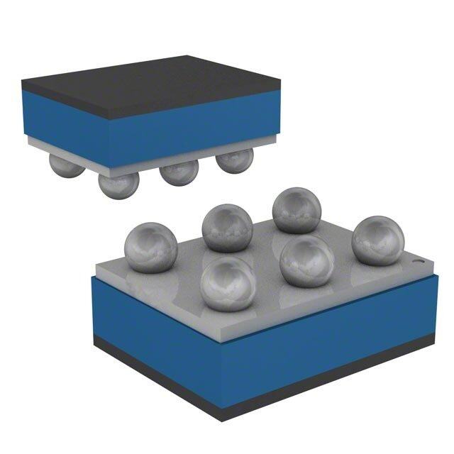
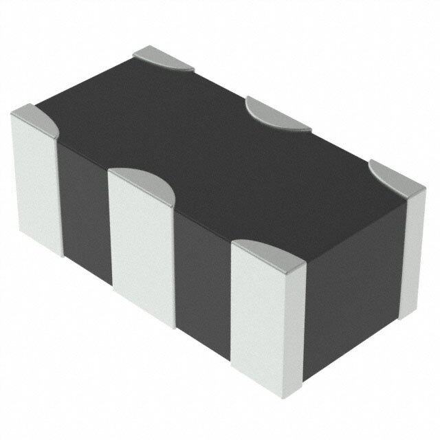
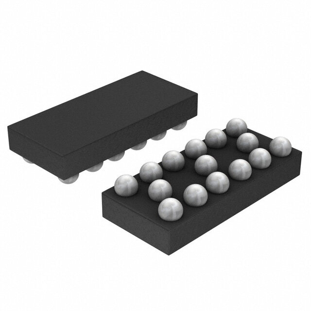
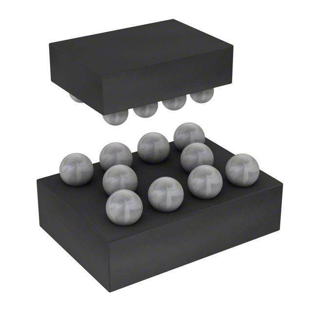
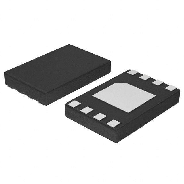
| 产品图片 |
|
| rohs | 符合RoHS尚未确定供货商 / 尚未确定供货商 |
| 产品系列 | EMI网络滤波器阵列,ON Semiconductor CM1457-04CPPraetorian III® |
| mouser_ship_limit | 该产品可能需要其他文件才能进口到中国。 |
| 数据手册 | |
| 产品型号 | CM1457-04CP |
| 中心/截止频率 | 300MHz(截止值) |
| 产品 | EMI Network Filter Arrays |
| 产品种类 | EMI网络滤波器阵列 |
| 元件数量 | 10 |
| 包装 | 带卷 (TR) |
| 商标 | ON Semiconductor |
| 外壳宽度 | 1.05 mm |
| 外壳长度 | 1.67 mm |
| 外壳高度 | 0.69 mm |
| 大小/尺寸 | 0.066" 长 x 0.041" 宽(1.67mm x 1.05mm) |
| 封装 | Reel |
| 封装/外壳 | 10-WFBGA,WLCSP |
| 封装/箱体 | CSP-10 |
| 工作温度 | -40°C ~ 85°C |
| 工作温度范围 | - 40 C to + 85 C |
| 工厂包装数量 | 3500 |
| 应用 | 移动设备的数据线路 |
| 截止频率 | 300 MHz |
| 技术 | LC(Pi) |
| 数值 | L = 70nH(总计),C = 20pF |
| 标准包装 | 3,500 |
| 滤波器阶数 | 5th |
| 电容 | 20 pF |
| 电感 | 70 nH |
| 电流 | 15mA |
| 电路类型 | LC (Pi) Filter |
| 电阻 | 45 Ohms |
| 电阻-通道(Ω) | 45 |
| 端接类型 | SMD/SMT |
| 类型 | EMI Filter Array with ESD Protection |
| 系列 | CM1457 |
| 衰减值 | 35dB @ 800MHz ~ 2.7GHz |
| 通道数 | 4 |
| 通道数量 | 4 Channel |
| 频率范围 | 800 MHz to 2.7 GHz |
| 高度 | 0.027"(0.69mm) |


- 商务部:美国ITC正式对集成电路等产品启动337调查
- 曝三星4nm工艺存在良率问题 高通将骁龙8 Gen1或转产台积电
- 太阳诱电将投资9.5亿元在常州建新厂生产MLCC 预计2023年完工
- 英特尔发布欧洲新工厂建设计划 深化IDM 2.0 战略
- 台积电先进制程称霸业界 有大客户加持明年业绩稳了
- 达到5530亿美元!SIA预计今年全球半导体销售额将创下新高
- 英特尔拟将自动驾驶子公司Mobileye上市 估值或超500亿美元
- 三星加码芯片和SET,合并消费电子和移动部门,撤换高东真等 CEO
- 三星电子宣布重大人事变动 还合并消费电子和移动部门
- 海关总署:前11个月进口集成电路产品价值2.52万亿元 增长14.8%

PDF Datasheet 数据手册内容提取
CM1457 4-, 6-, 8-Channel EMI Filter Array with ESD Protection Description The CM1457 is an inductor-based (L-C) EMI filter array with ESD protection, which integrates four, six, or eight filters in a CSP form http://onsemi.com factor with 0.40 mm pitch. Each EMI filter channel of the CM1457 is implemented with the component value of 6pF − 35nH – 4.7pF − 35nH – 1.8pF. The cut-off frequency at −3 dB attenuation is 300MHz and can be used in applications where the data rates are as high as 160 Mbps, while providing greater than −35 dB attenuation over the 800 MHz to 2.7 GHz frequency range. The parts include ESD WLCSP10 WLCSP15 WLCSP20 diodes on every I/O pin and provide a high level of protection against CP SUFFIX CP SUFFIX CP SUFFIX CASE 567BJ CASE 567BR CASE 567BV electrostatic discharge (ESD). The ESD protection diodes connected to the external filter ports are designed and characterized to safely dissipate ESD strikes of ±15 kV, which is beyond the maximum BLOCK DIAGRAM requirement of the IEC61000−4−2 international standard. 35 nH 35 nH This device is particularly well suited for wireless handsets, mobile Cn* An* LCD modules and PDAs because of its small package format and (External F F F (Internal easy-to-use pin assignments. In particular, the CM1457 is ideal for Pins) 6 p 7 p 8 p Pins) EMI filtering and protecting data and control lines for the LCD display 4. 1. GND and camera interface in mobile handsets. (Pins The CM1457 incorporates OptiGuard which results in improved B1−B4) reliability at assembly. It is manufactured with a 0.40mm pitch and 0.25mm CSP solder ball to provide up to 28% board space savings vs. competing CSP devices with 0.50mm pitch and 0.30mm CSP solder MARKING DIAGRAM ball. N57 w N57 yww N57 yyww Features • Four, Six or Eight Channels of EMI Filtering • ±15 kV ESD Protection (IEC 61000−4−2, Contact Discharge) at CM1457−04 CM1457−06 CM1457−08 10−Bump CSP 15−Bump CSP 20−Bump CSP External Pins • Greater than −40 dB of Attenuation at 1 GHz N57 = CM1457−04CP MIL−STD−883 International ESD Standard N57 = CM1457−06CP • N57 = CM1457−08CP Chip Scale Package (CSP) with 0.40 mm Pitch and 0.25 mm CSP w/yww/yyww = date code Solder Ball which Features Extremely Low Parasitic Inductance for Optimum Filter and ESD Performance • ORDERING INFORMATION OptiGuard Coating for Improved Reliability at Assembly • These Devices are Pb−Free and are RoHS Compliant Device Package Shipping† CM1457−04CP CSP−10 3500/Tape & Reel Applications • (Pb−Free) LCD and Camera Data Lines in Mobile Handsets • I/O Port Protection for Mobile Handsets, Notebook Computers, CM1457−06CP CSP−15 3500/Tape & Reel (Pb−Free) PDAs, etc. • EMI Filtering for Data Ports in Cell Phones, PDAs or Notebook CM1457−08CP CSP−20 3500/Tape & Reel Computers (Pb−Free) • Wireless Handsets †For information on tape and reel specifications, • Handheld PCs/PDAs including part orientation and tape sizes, please • refer to our Tape and Reel Packaging Specification LCD and Camera Modules Brochure, BRD8011/D. © Semiconductor Components Industries, LLC, 2013 1 Publication Order Number: May, 2013 − Rev. 6 CM1457/D
CM1457 PACKAGE / PINOUT DIAGRAMS Top View Bottom View (Bumps Down View) (Bumps Up View) Orientation Marking 1 2 3 4 + A C1 C2 C3 C4 B B1 B2 Orientation C Marking A1 A2 A3 A4 A1 CM1457−04CP 10−Bump CSP Orientation Marking 1 2 3 4 5 6 + A C1 C2 C3 C4 C5 C6 B B1 B2 B3 Orientation C Marking A1 A2 A3 A4 A5 A6 A1 CM1457−06CP 15−Bump CSP Orientation Marking 1 2 3 4 5 6 7 8 + A C1 C2 C3 C4 C5 C6 C7 C8 B B1 B2 B3 B4 Orientation C Marking A1 A2 A3 A4 A5 A6 A7 A8 A1 CM1457−08CP 20−Bump CSP Table 1. PIN DESCRIPTIONS Pin Number Pin Number −04 −06 −08 Pin Description −04 −06 −08 Pin Description A1 A1 A1 Filter #1 (Internal) C1 C1 C1 Filter #1 (External) A2 A2 A2 Filter #2 (Internal) C2 C2 C2 Filter #2 (External) A3 A3 A3 Filter #3 (Internal) C3 C3 C3 Filter #3 (External) A4 A4 A4 Filter #4 (Internal) C4 C4 C4 Filter #4 (External) − A5 A5 Filter #5 (Internal) − C5 C5 Filter #5 (External) − A6 A6 Filter #6 (Internal) − C6 C6 Filter #6 (External) − − A7 Filter #7 (Internal) − − C7 Filter #7 (External) − − A8 Filter #8 (Internal) − − C8 Filter #8 (External) B1, B2 B1−B3 B1−B4 GND http://onsemi.com 2
CM1457 SPECIFICATIONS Table 2. ABSOLUTE MAXIMUM RATINGS Parameter Rating Units Storage Temperature Range −65 to +150 °C DC current per Inductor 15 mA DC Package Power Rating 0.5 W Stresses exceeding Maximum Ratings may damage the device. Maximum Ratings are stress ratings only. Functional operation above the Recommended Operating Conditions is not implied. Extended exposure to stresses above the Recommended Operating Conditions may affect device reliability. Table 3. STANDARD OPERATING CONDITIONS Parameter Rating Units Operating Temperature Range −40 to +85 °C Table 4. ELECTRICAL OPERATING CHARACTERISTICS (Note 1) Symbol Parameter Conditions Min Typ Max Units LTOT Total Channel Inductance 70 nH RTOT Total Channel DC Resistance 45 (cid:2) CTOT_0V Total Channel Capacitance, 0 V bias 0 V dc; 1 MHz, 30 mV rms 20 24 pF CTOT_2.5V Total Channel Capacitance, 2.5 V bias 2.5 V dc; 1 MHz, 12.5 pF 30 mV rms VST Stand−off Voltage I = 10 (cid:3)A 5.5 V ILEAK Diode Leakage Current VIN = +3.3 V 0.1 0.5 (cid:3)A VSIG Signal Clamp Voltage V Positive Clamp ILOAD = 10 mA 5.6 6.8 9.0 Negative Clamp ILOAD = −10 mA −1.5 −0.8 −0.4 VESD In−system ESD Withstand Voltage (Notes 2 and 3) kV a) Contact Discharge per IEC 61000−4−2 standard, ±15 Level 4 (External Pins) b) Contact Discharge per IEC 61000−4−2 standard, ±2 Level 4 (Internal Pins) fC Cut−off Frequency MHz ZSOURCE = 50 (cid:2), ZLOAD = 50 (cid:2) 300 1. TA = 25°C unless otherwise specified. 2. ESD applied to input and output pins with respect to GND, one at a time. 3. Unused pins are left open. APPLICATION INFORMATION Refer to Application Note “The Chip Scale Package”, for a detailed description of Chip Scale Packages offered by ONSemiconductor. http://onsemi.com 3
CM1457 PERFORMANCE INFORMATION 0dB −10dB S S −20dB O L N O TI R E −30dB S N I −40dB −50dB 3 10 100 1000 2000 6000 FREQUENCY(MHz) Figure 1. Insertion Loss vs. Frequency (0 V Bias) 0dB −10dB S OS −20dB L N O TI R E S −30dB N I −40dB −50dB 3 10 100 1000 2000 6000 FREQUENCY(MHz) Figure 2. Insertion Loss vs. Frequency (2.5 V Bias) http://onsemi.com 4
CM1457 PACKAGE DIMENSIONS WLCSP10, 1.67x1.05 CASE 567BJ−01 ISSUE O NOTES: D A B 1. DIMENSIONING AND TOLERANCING PER REFERPEINN CAE1 È 2. ACSOMNETR YO1L4L.5INMG, 1 D99IM4.ENSION: MILLIMETERS. 3. COPLANARITY APPLIES TO SPHERICAL È CROWNS OF SOLDER BALLS. E MILLIMETERS 2X 0.05 C DIM MIN MAX A 0.54 0.69 A1 0.17 0.24 2X 0.05 C A2 0.42 REF TOP VIEW b 0.24 0.29 D 1.67 BSC OptiGuard Option A2 E 1.05 BSC eD 0.400 BSC 0.05 C ÉÉÉÉ eE 0.347 BSC A RECOMMENDED SOLDERING FOOTPRINT* 0.05 C NOTE 3 A1 SIDE VIEW C SPELAATNIENG A1 POAUCTKLAINGEE eD/2 0.35 10X b eD 0.05 C A B eE 0.35 10X 0.25 0.03 C C 0.40 B PITCH DIMENSIONS: MILLIMETERS A *For additional information on our Pb−Free strategy and soldering 1 2 3 4 5 6 details, please download the ON Semiconductor Soldering and BOTTOM VIEW Mounting Techniques Reference Manual, SOLDERRM/D. http://onsemi.com 5
CM1457 PACKAGE DIMENSIONS WLCSP15, 2.47x1.05 CASE 567BR−01 ISSUE O NOTES: D A B 1. DIMENSIONING AND TOLERANCING PER REFERPEINN CAE1 È 2. ACSOMNETR YO1L4L.5INMG, 1 D99IM4.ENSION: MILLIMETERS. 3. COPLANARITY APPLIES TO SPHERICAL È CROWNS OF SOLDER BALLS. E MILLIMETERS 2X 0.05 C DIM MIN MAX A 0.54 0.69 A1 0.17 0.24 2X 0.05 C A2 0.42 REF TOP VIEW b 0.24 0.29 D 2.47 BSC OptiGuard Option A2 E 1.05 BSC eD 0.400 BSC 0.05 C ÉÉÉÉÉÉ eE 0.347 BSC A RECOMMENDED SOLDERING FOOTPRINT* 0.05 C NOTE 3 A1 SIDE VIEW C SPELAATNIENG A1 POAUCTKLAINGEE eD/2 0.35 15X b eD 0.05 C A B eE 0.35 15X 0.03 C C 0.40 0.25 B PITCH DIMENSIONS: MILLIMETERS A *For additional information on our Pb−Free strategy and soldering 1 2 3 4 5 6 7 8 9 details, please download the ON Semiconductor Soldering and BOTTOM VIEW Mounting Techniques Reference Manual, SOLDERRM/D. http://onsemi.com 6
CM1457 PACKAGE DIMENSIONS WLCSP20, 3.27x1.05 CASE 567BV−01 ISSUE O NOTES: D A B 1. DIMENSIONING AND TOLERANCING PER PIN A1 ÈÈ ASME Y14.5M, 1994. REFERENCE 2. CONTROLLING DIMENSION: MILLIMETERS. 3. COPLANARITY APPLIES TO SPHERICAL ÈÈ CROWNS OF SOLDER BALLS. E MILLIMETERS 2X 0.05 C DIM MIN MAX A 0.54 0.69 A1 0.17 0.24 2X 0.05 C A2 0.42 REF TOP VIEW b 0.24 0.29 D 3.27 BSC OptiGuard Option A2 E 1.05 BSC eD 0.400 BSC 0.05 C ÉÉÉÉÉÉÉÉ eE 0.347 BSC A 0.05 C NOTE 3 A1 SIDE VIEW C SPELAATNIENG eD/2 20X b eD 0.05 C A B eE 0.03 C C B A 1 2 3 4 5 6 7 8 9 101112 BOTTOM VIEW RECOMMENDED SOLDERING FOOTPRINT* A1 POAUCTKLAINGEE 0.35 0.35 20X 0.25 0.40 PITCH DIMENSIONS: MILLIMETERS *For additional information on our Pb−Free strategy and soldering details, please download the ON Semiconductor Soldering and Mounting Techniques Reference Manual, SOLDERRM/D. ON Semiconductor and are registered trademarks of Semiconductor Components Industries, LLC (SCILLC). SCILLC owns the rights to a number of patents, trademarks, copyrights, trade secrets, and other intellectual property. A listing of SCILLC’s product/patent coverage may be accessed at www.onsemi.com/site/pdf/Patent−Marking.pdf. SCILLC reserves the right to make changes without further notice to any products herein. SCILLC makes no warranty, representation or guarantee regarding the suitability of its products for any particular purpose, nor does SCILLC assume any liability arising out of the application or use of any product or circuit, and specifically disclaims any and all liability, including without limitation special, consequential or incidental damages. “Typical” parameters which may be provided in SCILLC data sheets and/or specifications can and do vary in different applications and actual performance may vary over time. All operating parameters, including “Typicals” must be validated for each customer application by customer’s technical experts. SCILLC does not convey any license under its patent rights nor the rights of others. SCILLC products are not designed, intended, or authorized for use as components in systems intended for surgical implant into the body, or other applications intended to support or sustain life, or for any other application in which the failure of the SCILLC product could create a situation where personal injury or death may occur. Should Buyer purchase or use SCILLC products for any such unintended or unauthorized application, Buyer shall indemnify and hold SCILLC and its officers, employees, subsidiaries, affiliates, and distributors harmless against all claims, costs, damages, and expenses, and reasonable attorney fees arising out of, directly or indirectly, any claim of personal injury or death associated with such unintended or unauthorized use, even if such claim alleges that SCILLC was negligent regarding the design or manufacture of the part. SCILLC is an Equal Opportunity/Affirmative Action Employer. This literature is subject to all applicable copyright laws and is not for resale in any manner. PUBLICATION ORDERING INFORMATION LITERATURE FULFILLMENT: N. American Technical Support: 800−282−9855 Toll Free ON Semiconductor Website: www.onsemi.com Literature Distribution Center for ON Semiconductor USA/Canada P.O. Box 5163, Denver, Colorado 80217 USA Europe, Middle East and Africa Technical Support: Order Literature: http://www.onsemi.com/orderlit Phone: 303−675−2175 or 800−344−3860 Toll Free USA/Canada Phone: 421 33 790 2910 Fax: 303−675−2176 or 800−344−3867 Toll Free USA/Canada Japan Customer Focus Center For additional information, please contact your local Email: orderlit@onsemi.com Phone: 81−3−5817−1050 Sales Representative http://onsemi.com CM1457/D 7
Mouser Electronics Authorized Distributor Click to View Pricing, Inventory, Delivery & Lifecycle Information: O N Semiconductor: CM1457-04CP CM1457-06CP CM1457-08CP