 Datasheet下载
- 型号: CDDFN10-3304N
- 制造商: Bourns
- 库位|库存: xxxx|xxxx
- 要求:
| 数量阶梯 | 香港交货 | 国内含税 |
| +xxxx | $xxxx | ¥xxxx |
查看当月历史价格
查看今年历史价格
CDDFN10-3304N产品简介:
ICGOO电子元器件商城为您提供CDDFN10-3304N由Bourns设计生产,在icgoo商城现货销售,并且可以通过原厂、代理商等渠道进行代购。 CDDFN10-3304N价格参考¥询价-¥询价。BournsCDDFN10-3304N封装/规格:TVS - 二极管, 20V Clamp 25A (8/20µs) Ipp Tvs Diode Surface Mount 10-DFN (2.5x2.5)。您可以下载CDDFN10-3304N参考资料、Datasheet数据手册功能说明书,资料中有CDDFN10-3304N 详细功能的应用电路图电压和使用方法及教程。
Bourns Inc. 的型号 CDDFN10-3304N 属于TVS(瞬态电压抑制)二极管,主要用于电路中的过电压和静电放电(ESD)保护。该器件采用紧凑型DFN封装,具有响应速度快、箝位电压低、可靠性高等特点,适用于对空间要求高且需高效保护的电子设备。

典型应用场景包括:便携式消费类电子产品(如智能手机、平板电脑、笔记本电脑),用于保护数据接口(USB、HDMI、音频接口等)免受ESD冲击;通信设备中的高速信号线防护;工业控制模块中敏感电路的瞬态干扰抑制;以及汽车电子中的车载信息娱乐系统和传感器接口保护。

CDDFN10-3304N 具有多通道设计(通常为4通道),可同时保护多条信号线,额定功率适中,适合处理IEC 61000-4-2规定的±15kV空气放电和接触放电事件。其低电容特性确保了对高速信号完整性的影响最小,因此广泛应用于高频信号线路的ESD防护。

综上,该TVS二极管适用于需要小型化、高性能ESD保护的各类电子系统,尤其在消费电子、通信和汽车电子领域表现突出。
| 参数 | 数值 |
| 产品目录 | |
| 描述 | TVS DIODE 3.3VWM 20VC DFN10TVS二极管阵列 TVS Diode Array 3.3VOLT |
| 产品分类 | |
| 品牌 | Bourns Inc. |
| 产品手册 | |
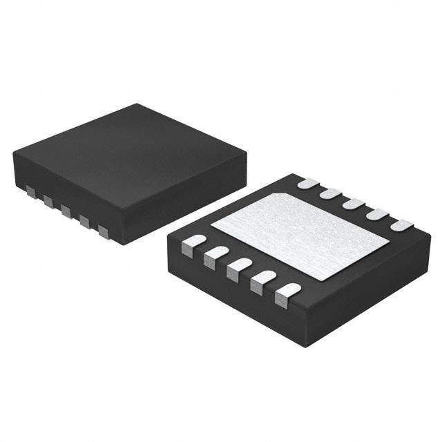
| 产品图片 |
|
| rohs | 符合RoHS无铅 / 符合限制有害物质指令(RoHS)规范要求 |
| 产品系列 | 二极管与整流器,TVS二极管,TVS二极管阵列,Bourns CDDFN10-3304N- |
| 数据手册 | |
| 产品型号 | CDDFN10-3304N |
| PCN组件/产地 | |
| PCN设计/规格 | |
| 不同频率时的电容 | 4pF @ 1MHz |
| 产品种类 | TVS二极管阵列 |
| 供应商器件封装 | 10-DFN (2.5x2.5) |
| 其它名称 | CDDFN10-3304N-ND |
| 击穿电压 | 3.9 V |
| 功率-峰值脉冲 | 450W |
| 包装 | 带卷 (TR) |
| 单向通道 | - |
| 双向通道 | 4 |
| 商标 | Bourns |
| 外壳高度 | 0.5 mm |
| 安装类型 | 表面贴装 |
| 安装风格 | SMD/SMT |
| 封装 | Reel |
| 封装/外壳 | 10-UFDFN 裸露焊盘 |
| 封装/箱体 | DFN-10 |
| 尺寸 | 2.45 mm W x 2.45 mm L x 0.5 mm H |
| 峰值浪涌电流 | 25 A |
| 峰值脉冲功率耗散 | 450 W |
| 工作温度 | -55°C ~ 125°C (TA) |
| 工作电压 | 3.3 V |
| 工厂包装数量 | 3000 |
| 应用 | 以太网 |
| 最大工作温度 | + 150 C |
| 最小工作温度 | - 55 C |
| 标准包装 | 3,000 |
| 电压-击穿(最小值) | 3.9V |
| 电压-反向关态(典型值) | 3.3V (最小值) |
| 电压-箝位(最大值)@Ipp | 20V |
| 电容 | 4 pF |
| 电流-峰值脉冲(10/1000µs) | 25A (8/20µs) |
| 电源线路保护 | 是 |
| 端接类型 | SMD/SMT |
| 类型 | 转向装置(轨至轨) |
| 系列 | CDDFN10 |
| 通道 | 4 Channels |
| 钳位电压 | 15 V |


- 商务部:美国ITC正式对集成电路等产品启动337调查
- 曝三星4nm工艺存在良率问题 高通将骁龙8 Gen1或转产台积电
- 太阳诱电将投资9.5亿元在常州建新厂生产MLCC 预计2023年完工
- 英特尔发布欧洲新工厂建设计划 深化IDM 2.0 战略
- 台积电先进制程称霸业界 有大客户加持明年业绩稳了
- 达到5530亿美元!SIA预计今年全球半导体销售额将创下新高
- 英特尔拟将自动驾驶子公司Mobileye上市 估值或超500亿美元
- 三星加码芯片和SET,合并消费电子和移动部门,撤换高东真等 CEO
- 三星电子宣布重大人事变动 还合并消费电子和移动部门
- 海关总署:前11个月进口集成电路产品价值2.52万亿元 增长14.8%


PDF Datasheet 数据手册内容提取
NT *RoHS VCEOARVMSIAPILOLINAASB LE Features Applications NT MPLIA n Working voltage 3.3 V n FireWire, T1/E1, T3/E3 chip side protection O HS C n SMT - DFN package n Digital Visual Interface (DVI) Ro * n Low capacitance - 4 pF n Ethernet 10/100/1000 Base T n IEC 61000-4-2 (ESD) n High speed port protection n IEC 61000-4-4 (EFT) n Portable electronics n IEC 61000-4-5 (Surge) REE D F LEA CDDFN10-3304N - TVS/Steering Diode Array General Information Td(Sahutear g CpeDo) rDrtesF qmNu1eir0ee-tm3in3eg0n I4tEsN.C Td 6he1ev0 iTc0er0a -pn4rs-oi2ev ni(dEte SVsoD El)LtVEaS,E ARgIDDH SEISFe O,RCC NEOSESE MA6uFPRL1IEpT A0pN Ta0r*en0sd-4s So-4ur ra(gErerFa Tpy,r) o patrenocdtte iIocEntCin f go6 r1u h0pi0 gt0oh- 44s-p 5de aetda P5in lines, offers a Working Peak Voltage of 3.R3o V. Pin Pin Pin Pin 1 3 7 9 The DFN-10 packaged device will mount directly onto the industry standard DFN-10 footprint. Bourns® Chip Diodes are easy to handle with standard pick and place equipment. GND Absolute Maximum Ratings, TA = 25 °C (Unless Otherwise Noted) Parameter Symbol CDDFN10-3304N Unit Peak Pulse Power (tp = 8/20 µs) (NOTE 1) PPK 450 W Peak Pulse Current (tp = 8/20 µs) per IEC 61000-4-5 IPP 25 A Storage Temperature TSTG -55 to +150 ºC Operating Temperature TOPR -55 to +125 ºC ESD Protection per IEC 61000-4-2 kV Contact Discharge 30 max. kV Air Discharge 30 max. EFT Protection per IEC 61000-4-4 @ 5/50 ns 40 min. A Notes: 1. See Peak Pulse Power vs. Pulse Time. Electrical Characteristics (@ TA = 25 °C Unless Otherwise Noted) Parameter Symbol Min. Typ. Max. Unit Breakdown Voltage @ 1 mA VBR 3.9 V Working Peak Voltage VWM 3.3 V Leakage Current1 @ VWM ID 1 µA Clamping Voltage2 @ IP = 5 A 8/20 µs VC 15 V Clamping Voltage2 @ IP = 15 A 8/20 µs VC 18 V Clamping Voltage2 @ IP = 20 A 8/20 µs VC 20 V Junction Capacitance2 @ 0 V 1 MHz CD 4.0 5.0 pF Junction Capacitance3 @ 0 V 1 MHz CIO 1.5 pF Note 1: Pin 5 to ground. Note 2: Pin 1,3,7 or 9 to ground. Note 3: Between Pin 1,3,7 and 9. *RoHS Directive 2002/95/EC Jan. 27, 2003 including annex and RoHS Recast 2011/65/EU June 8, 2011. Specifications are subject to change without notice. The device characteristics and parameters in this data sheet can and do vary in different applications and actual device performance may vary over time. Users should verify actual device performance in their specific applications.
CDD33F1N21 0-- 233 m04mN S- MTVDS /TSrtiememriningg D Pioodtee nAtriroamyeter Rating & Characteristic Curves Peak Pulse Power vs. Pulse Time Pulse Waveform P – Peak Pulse (W)PP 101,100000000 450 W, 8/20 µs Waveform – Peak Pulse Current (% of I)PP 11246802000000 tt td =e tt|tTtItdP e =P=s/ t282 W 0µ saµvseform Parameters 10 I PP 0 0.01 1 10 100 1,000 10,000 0 5 10 15 20 25 30 td – Pulse Duration (µs) t – Time (µs) Clamping Voltage vs Peak Pulse Current Clamping Voltage vs Peak Pulse Current 22 24 20 22 18 Any I/O Pin to GND 20 Any I/O Pin to Another I/O Pin 16 18 Voltage (V) 1142 Voltage (V) 111642 mping 108 mping 10 Cla 6 Waveform Cla 86 Waveform 4 Parameters: 4 Parameters: tr = 8 µs tr = 8 µs 2 td = 20 µs 2 td = 20 µs 0 0 0 5 10 15 20 25 0 5 10 15 20 25 Peak Pulse Current (A) Peak Pulse Current (A) Typical Voltage vs. Capacitance Power Derating Curve 4.5 4.0 Any I/O Pin to GND 3.5 100 Peak Pulse Power pF) 3.0 8/20 µs e ( 80 nc 2.5 pacita 2.0 ower 60 a P nput C 1.5 Rated 40 I of 1.0 % VDD = Floating, GND = 0 V, 20 0.5 f = 1 MHz, T = 25 °C Average Power 0.0 0 0.0 0.5 1.0 1.5 2.0 2.5 3.0 3.5 0 25 50 75 100 125 150 Input Voltage (V) TL - Lead Temperature (°C) Specifications are subject to change without notice. The device characteristics and parameters in this data sheet can and do vary in different applications and actual device performance may vary over time. Users should verify actual device performance in their specific applications.
C3D31D2F N- 120 m-3m30 4SNM -D T TVrSi/mStmeeinrign gP oDtieondtei oAmrreatyer Product Dimensions Recommended Footprint 2.45 - 2.55 This is a molded DFN10 package with l(e0a.0d96 f-r e0.e10 0N)ickel-Paladium- 0.50 0.30 Gold (Ni/Pd/Au) on the lead frame. It has a flammability rating of (.020) (.012) UL 94V-0. 2.45 - 2.55 3.15 (0.096 - 0.100) 0.50 (.124) 0.30 (.020) (.012) 2.45 - 2.55 (0.096 - 0.100) 1.26 2.50 3.15 (1.0.8753) (.050) (.100) PIN 1 (.124) INDICATOR 2.45 - 2.55 (0.096 - 0.100) 1.26 2.50 1.85 (.050) (.100) PIN 1 (.073) DIMENSIONS: MM INDICATOR 0.65 2.05 (INCHES) (.026) (.081) 0.50 - 0.60 (0.020 - 0.024) Typi0c.6a5l Part Marki2n.0g5 (.026) (.081) 0.152 0.50 - 0.60 (0.006) (0.020 - 0.024) DEVICE CODE: Week Duration 334 = CDDFN10-3304N Code 0.20 - 0.30 0.50 (0.008 - 0.012) (0.020) 2 Week 1~Week 7 0.152 (0.006) 334 3 Week 8~Week 14 YWLLL 0.20 - 0.30 PIN 1 0.50 4 Week 15~Week 21 (0.008 - 0.012) (0.020) R (.00.028) 1.15 - 1.25 DATE CODE 5 Week 22~Week 28 YEAR CODE: LOT (0.045 - 0.049) 5 = 2015 TRACEABILITY 6 Week 29~Week 35 PIN 1 6 = 2016 CODE WEEK CODE: 7 Week 36~Week 42 R (.00.028) 1.15 - 1.25 45 == WWEEEEKK 1252 ttoo WWEEEEKK 2218 8 Week 43~Week 49 (0.045 - 0.049) 9 Week 50~Week 52 0.35 - 0.45 1.85 - 1.95 (0.073 - 0.077) (0.014 - 0.018) 2.10 - 2.20 Pin Out (0.083 - 0.087) 0.35 - 0.45 1.85 - 1.95 (0.073 - 0.077) (0.014 - 0.018) Pin Function 2.10 - 2.20 1 I/O (0.083 - 0.087) 2 N.C. CH1 1 10 NC 3 I/O How to Order NC 2 9 CH2 4 N.C. CD DFN10 - 33 04 N CH3 3 GND 8 NC 5 VCC (CENTER TAB) Common Diode Chip Diode NC 4 7 CH4 6 N.C. Package 7 I/O VDD 5 6 NC DFN10 = DFN-10 Package 8 N.C. Working Peak Voltage TOP VIEW 33 = 3.3 VRWM (Volts) 9 I/O Number of Lines 10 N.C. 04 = 4 Data Lines Suffix CENTER GROUND N = Low Capacitance TAB Specifications are subject to change without notice. The device characteristics and parameters in this data sheet can and do vary in different applications and actual device performance may vary over time. Users should verify actual device performance in their specific applications.
CDDFN10-3304N - TVS/Steering Diode Array Packaging Information The product will be dispensed in tape and reel format (see diagram below). P 0 P1 E T d Index Hole Pin 1 Location 120 ° F D2 W B D1 D P A C Trailer Device Leader ....... ....... ....... ....... W1 End ....... ....... ....... ....... Start MM DIMENSIONS: (INCHES) 10 pitches (min.) 10 pitches (min.) Devices are packed in accordance with EIA standard Direction of Feed RS-481-A. Item Symbol DFN-10 2.80 ± 0.10 Carrier Width A (0.110 ± 0.004) 2.85 ± 0.10 Carrier Length B (0.112 ± 0.004) 1.00 ± 0.05 Carrier Depth C (0.039 ± 0.002) 1.50 +0.10/-0 Sprocket Hole d (0.059 +0.004/-0) 180 ± 3 Reel Outside Diameter D (7.087 ± 0.118) 50.0 Reel Inner Diameter D1 (1.969) MIN. 13.00 +0.50/-0.20 Feed Hole Diameter D2 (0.512 +0.020/-0.008) 1.75 ± 0.10 Sprocket Hole Position E (0.069 ± 0.004) 5.50 ± 0.05 Punch Hole Position F (0.217 ± 0.002) 4.00 ± 0.10 Punch Hole Pitch P (0.157 ± 0.004) 4.00 ± 0.10 Sprocket Hole Pitch P0 (0.157 ± 0.004) 2.00 ± 0.05 Embossment Center P1 (0.079 ± 0.002) 0.60 Overall Tape Thickness T MAX. (0.024) 12.3 Tape Width W (0.484) MAX. REV. 08/16 18.4 Specifications are subject to change without notice. Reel Width W1 (0.724) MAX. The device characteristics and parameters in this data sheet can and do vary in different applications and actual device performance may vary over time. Quantity per Reel -- 3000 Users should verify actual device performance in their specific applications.